CN115706100A - Electronic device - Google Patents
Electronic device Download PDFInfo
- Publication number
- CN115706100A CN115706100A CN202210411559.8A CN202210411559A CN115706100A CN 115706100 A CN115706100 A CN 115706100A CN 202210411559 A CN202210411559 A CN 202210411559A CN 115706100 A CN115706100 A CN 115706100A
- Authority
- CN
- China
- Prior art keywords
- semiconductor element
- electronic device
- substrate
- protection structure
- protection
- Prior art date
- Legal status (The legal status is an assumption and is not a legal conclusion. Google has not performed a legal analysis and makes no representation as to the accuracy of the status listed.)
- Pending
Links
Images


Landscapes
- Structures Or Materials For Encapsulating Or Coating Semiconductor Devices Or Solid State Devices (AREA)
Abstract
本揭露提供一种电子装置,包括基板、第一半导体元件以及第一保护结构。第一半导体元件设置于基板上且电性连接基板。第一半导体元件具有远离基板的第一表面。第一保护结构覆盖至少部分的第一表面。
The disclosure provides an electronic device, including a substrate, a first semiconductor element, and a first protection structure. The first semiconductor element is disposed on the substrate and electrically connected to the substrate. The first semiconductor element has a first surface away from the substrate. The first protection structure covers at least part of the first surface.
Description
技术领域technical field
本揭露涉及一种电子装置,尤其涉及一种具有较佳结构可靠度的电子装置。The present disclosure relates to an electronic device, in particular to an electronic device with better structural reliability.
背景技术Background technique
当现有技术中的微电子元件(例如是集成电路(Integrated Circuit)或发光二极管(micro LED)等)以玻璃为载体时,在将微电子元件切割时,或是,将微电子元件接合至基板(或电路板)时的应力或撞击力等,皆可使载体或其上的电路膜层在切割边或角落处产生裂缝(crack),进而影响到产品的品质及结构可靠度。When microelectronic components in the prior art (such as integrated circuits (Integrated Circuit) or light-emitting diodes (micro LED), etc.) use glass as a carrier, when the microelectronic components are cut, or the microelectronic components are bonded to The stress or impact force of the substrate (or circuit board) can cause cracks on the cutting edge or corner of the carrier or the circuit film layer on it, which will affect the quality and structural reliability of the product.
发明内容Contents of the invention
根据本揭露的实施例,电子装置包括基板、第一半导体元件以及第一保护结构。第一半导体元件设置于基板上且电性连接基板。第一半导体元件具有远离基板的第一表面。第一保护结构覆盖至少部分的第一表面。According to an embodiment of the present disclosure, an electronic device includes a substrate, a first semiconductor element, and a first protection structure. The first semiconductor element is disposed on the substrate and electrically connected to the substrate. The first semiconductor element has a first surface away from the substrate. The first protection structure covers at least part of the first surface.
附图说明Description of drawings
图1A是本揭露的一实施例的一种电子装置的示意图;FIG. 1A is a schematic diagram of an electronic device according to an embodiment of the present disclosure;
图1B是图1A的电子装置的第一半导体元件的俯视示意图;FIG. 1B is a schematic top view of a first semiconductor element of the electronic device of FIG. 1A;
图1C是沿图1B的线I-I的剖面示意图;Fig. 1C is a schematic cross-sectional view along the line I-I of Fig. 1B;
图2是本揭露的另一实施例的一种电子装置的示意图;FIG. 2 is a schematic diagram of an electronic device according to another embodiment of the present disclosure;
图3是本揭露的另一实施例的一种第一半导体元件的剖面示意图;3 is a schematic cross-sectional view of a first semiconductor element according to another embodiment of the present disclosure;
图4A是本揭露的另一实施例的一种电子装置的侧视示意图;FIG. 4A is a schematic side view of an electronic device according to another embodiment of the present disclosure;
图4B是图4A的电子装置的俯视示意图;FIG. 4B is a schematic top view of the electronic device of FIG. 4A;
图5是本揭露的另一实施例的一种电子装置的示意图;FIG. 5 is a schematic diagram of an electronic device according to another embodiment of the present disclosure;
图6是本揭露的另一实施例的一种电子装置的侧视示意图;6 is a schematic side view of an electronic device according to another embodiment of the present disclosure;
图7是本揭露的另一实施例的一种电子装置的侧视示意图;7 is a schematic side view of an electronic device according to another embodiment of the present disclosure;
图8是本揭露的另一实施例的一种电子装置的侧视示意图;FIG. 8 is a schematic side view of an electronic device according to another embodiment of the present disclosure;
图9是本揭露的另一实施例的一种电子装置的侧视示意图。FIG. 9 is a schematic side view of an electronic device according to another embodiment of the present disclosure.
附图标记说明Explanation of reference signs
100a、100b、100c、100d、100e、100f、100g、100h、100i:电子装置;100a, 100b, 100c, 100d, 100e, 100f, 100g, 100h, 100i: electronic devices;
110:基板;110: substrate;
113:基底;113: base;
112:上表面;112: upper surface;
115:线路层;115: line layer;
117:导电通孔;117: conductive via;
122a、124a、122c、124d、124e、124f、124g、124h、124i:第一半导体元件;122a, 124a, 122c, 124d, 124e, 124f, 124g, 124h, 124i: first semiconductor element;
123a、123c、P:接垫;123a, 123c, P: pads;
125a、125c:载板;125a, 125c: carrier board;
126a、126d、126e、126f、126g、126h、126i:第二半导体元件;126a, 126d, 126e, 126f, 126g, 126h, 126i: second semiconductor elements;
127a、127c:芯片本体;127a, 127c: chip body;
128a、128e:第三半导体元件;128a, 128e: the third semiconductor element;
129a、129c:缓冲层;129a, 129c: buffer layer;
130b、130c、130d、130e、130f、130g、130h、130i:第一保护结构;130b, 130c, 130d, 130e, 130f, 130g, 130h, 130i: first protective structure;
132a、132f、132h:第一保护层;132a, 132f, 132h: first protective layer;
134a、134f、134h:第二保护层;134a, 134f, 134h: second protective layer;
140:材料层;140: material layer;
150:隔墙结构;150: Partition wall structure;
160:光学膜片组;160: optical diaphragm group;
170e、170g、170i:第二保护结构;170e, 170g, 170i: second protective structure;
S11、S12、S21、S31、S41、S51、S61、S71、S81、S91:第一表面;S11, S12, S21, S31, S41, S51, S61, S71, S81, S91: the first surface;
S13、S42、S52、S62、S72、S82、S92:第二表面;S13, S42, S52, S62, S72, S82, S92: the second surface;
S14、S53:第三表面;S14, S53: the third surface;
W1、W2、W3、W4、W5、W6、W7、W8:宽度;W1, W2, W3, W4, W5, W6, W7, W8: width;
L:打线。L: Line up.
具体实施方式Detailed ways
以下针对本揭露实施例的电子装置作详细说明。应了解的是,以下的叙述提供许多不同的实施例,用以实施本揭露一些实施例的不同态样。以下所述特定的元件及排列方式仅为简单清楚描述本揭露一些实施例。当然,这些仅用以举例而非本揭露的限定。此外,在不同实施例中可能使用类似和/或对应的标号标示类似和/或对应的元件,以清楚描述本揭露。然而,这些类似和/或对应的标号的使用仅为了简单清楚地叙述本揭露一些实施例,不代表所讨论的不同实施例和/或结构之间具有任何关连性。The electronic device according to the embodiment of the present disclosure will be described in detail below. It should be understood that the following description provides many different embodiments for implementing different aspects of some embodiments of the present disclosure. The specific components and arrangements described below are only for simple and clear description of some embodiments of the present disclosure. Of course, these are only examples rather than limitations of the present disclosure. In addition, similar and/or corresponding reference numerals may be used in different embodiments to denote similar and/or corresponding elements to clearly describe the present disclosure. However, the use of these similar and/or corresponding symbols is only for simply and clearly describing some embodiments of the present disclosure, and does not mean that there is any relationship between the different embodiments and/or structures discussed.
应理解的是,实施例中可能使用相对性用语,例如“较低”或“底部”或“较高”或“顶部”,以描述附图的一个元件对于另一元件的相对关系。可理解的是,如果将附图的装置翻转使其上下颠倒,则所叙述在“较低”侧的元件将会成为在“较高”侧的元件。本揭露实施例可配合附图一并理解,本揭露的附图亦被视为揭露说明的一部分。应理解的是,本揭露的附图并未按照比例绘制,事实上,可能任意的放大或缩小元件的尺寸以便清楚表现出本揭露的特征。It should be understood that relative terms such as "lower" or "bottom" or "higher" or "top" may be used in the embodiments to describe the relative relationship of one element to another element of the drawings. It will be understood that if the device of the figures is turned over so that it is upside down, elements described as being on the "lower" side would then become elements on the "higher" side. The embodiments of the present disclosure can be understood together with the drawings, and the drawings of the present disclosure are also regarded as a part of the disclosure description. It should be understood that the drawings of the present disclosure are not drawn to scale and, in fact, the dimensions of elements may be arbitrarily enlarged or reduced in order to clearly illustrate the features of the present disclosure.
再者,当述及一第一材料层位于一第二材料层上或之上时,可能包含第一材料层与第二材料层直接接触的情形或第一材料层与第二材料层之间可能不直接接触,亦即第一材料层与第二材料层之间可能间隔有一或更多其他材料层的情形。但若第一材料层直接位于第二材料层上时,即表示第一材料层与第二材料层直接接触的情形。Furthermore, when it is mentioned that a first material layer is located on or over a second material layer, it may include the situation that the first material layer is in direct contact with the second material layer or the situation between the first material layer and the second material layer There may be no direct contact, that is, one or more other material layers may be separated between the first material layer and the second material layer. However, if the first material layer is directly on the second material layer, it means that the first material layer is in direct contact with the second material layer.
此外,应理解的是,说明书与权利要求中所使用的序数例如“第一”、“第二”等的用词用以修饰元件,其本身并不意涵及代表该(或该些)元件有任何之前的序数,也不代表某一元件与另一元件的顺序、或是制造方法上的顺序,该些序数的使用仅用来使具有某命名的元件得以和另一具有相同命名的元件能作出清楚区分。权利要求与说明书中可不使用相同用词,例如,说明书中的第一元件在权利要求中可能为第二元件。In addition, it should be understood that the ordinal numbers used in the description and claims, such as "first", "second", etc., are used to modify elements, which do not imply and represent that the (or these) elements have Any preceding ordinal numbers do not denote the order of one element with another, or the order of manufacturing methods, but are used only to enable an element with a certain designation to be compatible with another element with the same designation. Make a clear distinction. The claims and the description may not use the same words, for example, a first element in the description may be a second element in the claim.
在本揭露一些实施例中,关于接合、连接的用语例如“连接”、“互连”等,除非特别定义,否则可指两个结构系直接接触,或者亦可指两个结构并非直接接触,其中有其他结构设于此两个结构之间。且此关于接合、连接的用语亦可包含两个结构都可移动,或者两个结构都固定的情况。此外,用语“电性连接”或“电性耦接”包含任何直接及间接的电性连接手段。In some embodiments of the present disclosure, terms related to bonding and connection, such as "connection" and "interconnection", unless otherwise specified, may refer to two structures being in direct contact, or may also refer to two structures not in direct contact, There are other structures located between these two structures. In addition, the term "bonding" and "connection" may also include the case where both structures are movable, or both structures are fixed. In addition, the terms "electrically connected" or "electrically coupled" include any direct and indirect electrical connection means.
于文中,“约”、“实质上”的用语通常表示在一给定值或范围的10%内、或5%内、或3%之内、或2%之内、或1%之内、或0.5%之内。在此给定的数量为大约的数量,亦即在没有特定说明“约”、“实质上”的情况下,仍可隐含“约”、“实质上”的含义。用语“范围介于第一数值至第二数值之间”表示所述范围包含第一数值、第二数值以及它们之间的其他数值。再者,任两个用来比较的数值或方向,可存在着一定的误差。若第一数值等于第二数值,其隐含着第一数值与第二数值之间可存在着约10%的误差;若第一方向垂直于第二方向,则第一方向与第二方向之间的角度可介于80度至100度之间;若第一方向平行于第二方向,则第一方向与第二方向之间的角度可介于0度至10度之间。In the text, the terms "about" and "substantially" usually mean within 10%, or within 5%, or within 3%, or within 2%, or within 1%, of a given value or range. or within 0.5%. The given quantity here is an approximate quantity, that is, the meaning of "about" and "substantially" can still be implied if "about" and "substantially" are not specified. The term "a range between a first value and a second value" means that the range includes the first value, the second value and other values therebetween. Furthermore, any two values or directions used for comparison may have certain errors. If the first value is equal to the second value, it implies that there may be an error of about 10% between the first value and the second value; if the first direction is perpendicular to the second direction, the difference between the first direction and the second direction The angle between them may be between 80° and 100°; if the first direction is parallel to the second direction, the angle between the first direction and the second direction may be between 0° and 10°.
本揭露通篇说明书与后附的权利要求中会使用某些词汇来指称特定元件。本领域技术人员应理解,电子设备制造商可能会以不同的名称来指称相同的元件。本文并不意在区分那些功能相同但名称不同的元件。在下文说明书与申请专利范围中,“包括”、“含有”、“具有”等词为开放式词语,因此其应被解释为“含有但不限定为…”之意。因此,当本揭露的描述中使用术语“包括”、“含有”和/或“具有”时,其指定了相应的特征、区域、步骤、操作和/或元件的存在,但不排除一个或多个相应的特征、区域、步骤、操作和/或元件的存在。Certain terms will be used throughout the specification and claims that follow this disclosure to refer to particular elements. Those skilled in the art should understand that electronic device manufacturers may refer to the same element by different names. This document does not intend to distinguish between those elements that have the same function but have different names. In the following specification and scope of patent application, words such as "comprising", "containing", and "having" are open-ended words, so they should be interpreted as meaning "including but not limited to...". Therefore, when the terms "comprising", "comprising" and/or "having" are used in the description of the present disclosure, it specifies the existence of corresponding features, regions, steps, operations and/or elements, but does not exclude one or more The existence of a corresponding feature, region, step, operation and/or element.
应理解的是,以下所举实施例可以在不脱离本揭露的精神下,可将数个不同实施例中的特征进行替换、重组、结合以完成其他实施例。各实施例间特征只要不违背发明精神或相冲突,均可任意结合搭配使用。It should be understood that, in the following embodiments, without departing from the spirit of the present disclosure, features in several different embodiments may be replaced, reorganized, and combined to complete other embodiments. As long as the features of the various embodiments do not violate the spirit of the invention or conflict, they can be used in any combination and collocation.
此外,本揭露所揭示的电子装置可包含显示装置、背光装置、天线装置、感测装置、拼接装置、触控电子装置(touch display)、曲面电子装置(curved display)或非矩形电子装置(free shape display),但不以此为限。电子装置可例如包含液晶(liquid crystal)、发光二极管(light emitting diode)、荧光(luorescence)、磷光(phosphor)、其它合适的显示介质、或前述的组合,但不以此为限。显示装置可为非自发光型显示装置或自发光型显示装置。天线装置可为液晶型态的天线装置或非液晶型态的天线装置,感测装置可为感测电容、光线、热能或超声波的感测装置,但不以此为限。电子元件可包括被动元件与主动元件,例如电容、电阻、电感、二极管、晶体管等。二极管可包括发光二极管(light emittingdiode,LED)或光电二极管(photodiode)。发光二极管可例如包括有机发光二极管(organiclight emitting diode,OLED)、次毫米发光二极管(mini LED)、微发光二极管(micro LED)或量子点发光二极管(quantum dot LED),但不以此为限。拼接装置可例如是显示器拼接装置或天线拼接装置,但不以此为限。需注意的是,电子装置可为前述的任意排列组合,但不以此为限。此外,电子装置可为可弯折或可挠式电子装置。需注意的是,电子装置可为前述的任意排列组合,但不以此为限。此外,电子装置的外形可为矩形、圆形、多边形、具有弯曲边缘的形状或其他适合的形状。电子装置可以具有驱动系统、控制系统、光源系统、层架系统…等周边系统以支援显示装置、天线装置或拼接装置。为方便说明,下文将以电子装置为背光装置的态样进行说明,但本揭露不以此为限。In addition, the electronic device disclosed in this disclosure may include a display device, a backlight device, an antenna device, a sensing device, a splicing device, a touch display, a curved display, or a non-rectangular electronic device (free shape display), but not limited thereto. The electronic device may include, for example, liquid crystal, light emitting diode, fluorescence, phosphor, other suitable display media, or combinations thereof, but is not limited thereto. The display device can be a non-self-luminous display device or a self-luminous display device. The antenna device can be a liquid crystal type antenna device or a non-liquid crystal type antenna device, and the sensing device can be a sensing device for sensing capacitance, light, thermal energy or ultrasonic waves, but not limited thereto. Electronic components may include passive components and active components, such as capacitors, resistors, inductors, diodes, transistors, and the like. The diodes may include light emitting diodes (light emitting diodes, LEDs) or photodiodes (photodiodes). The light emitting diodes may include, for example, organic light emitting diodes (OLEDs), submillimeter light emitting diodes (mini LEDs), micro LEDs (micro LEDs) or quantum dot light emitting diodes (quantum dot LEDs), but are not limited thereto. The splicing device may be, for example, a display splicing device or an antenna splicing device, but is not limited thereto. It should be noted that, the electronic device can be any permutation and combination mentioned above, but not limited thereto. In addition, the electronic device can be a bendable or flexible electronic device. It should be noted that, the electronic device can be any permutation and combination mentioned above, but not limited thereto. In addition, the shape of the electronic device may be rectangular, circular, polygonal, with curved edges, or other suitable shapes. The electronic device may have peripheral systems such as a drive system, a control system, a light source system, a shelf system, etc. to support a display device, an antenna device or a splicing device. For the convenience of description, the electronic device is used as the backlight device for description below, but the disclosure is not limited thereto.
除非另外定义,在此使用的全部用语(包含技术及科学用语)具有与本揭露所属技术领域的技术人员通常理解的相同涵义。能理解的是,这些用语例如在通常使用的字典中定义用语,应被解读成具有与相关技术及本揭露的背景或上下文一致的意思,而不应以一理想化或过度正式的方式解读,除非在本揭露实施例有特别定义。Unless otherwise defined, all terms (including technical and scientific terms) used herein have the same meaning as commonly understood by one of ordinary skill in the art to which this disclosure belongs. It can be understood that these terms, such as those defined in commonly used dictionaries, should be interpreted as having meanings consistent with the background or context of the related technology and the present disclosure, and should not be interpreted in an idealized or overly formal manner, Unless otherwise specified in the disclosed embodiments.
现将详细地参考本揭露的示范性实施例,示范性实施例的实例说明于附图中。只要有可能,相同元件符号在附图和描述中用来表示相同或相似部分。Reference will now be made in detail to the exemplary embodiments of the present disclosure, examples of which are illustrated in the accompanying drawings. Wherever possible, the same reference numbers will be used in the drawings and description to refer to the same or like parts.
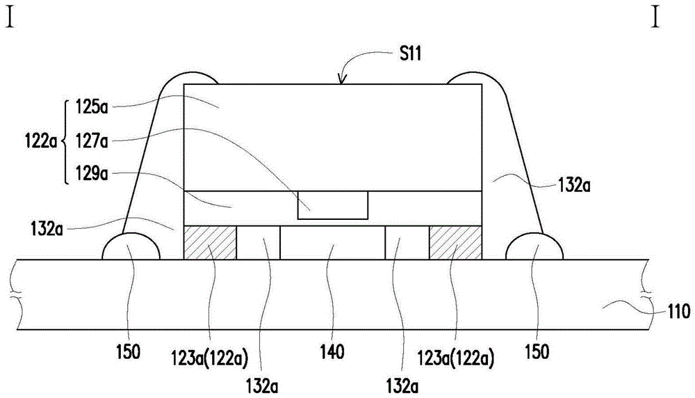
图1A是本揭露的一实施例的一种电子装置的示意图。图1B是图1A的电子装置的第一半导体元件的俯视示意图。图1C是沿图1B的线I-I的剖面示意图。为了方便说明,图1B是以透视的方式进行示出,并省略部分构件。FIG. 1A is a schematic diagram of an electronic device according to an embodiment of the present disclosure. FIG. 1B is a schematic top view of a first semiconductor element of the electronic device in FIG. 1A . FIG. 1C is a schematic cross-sectional view along line I-I of FIG. 1B . For convenience of description, FIG. 1B is shown in a perspective manner, and some components are omitted.
请先参考图1A,在本实施例中,电子装置100a包括基板110、第一半导体元件122a、第一半导体元件124a以及第一保护结构(例如第一保护结构132a及第一保护结构134a)。第一半导体元件122a及第一半导体元件124a设置于基板110上且电性连接基板110。第一半导体元件122a具有远离基板110的第一表面S11,而第一半导体元件124a具有远离基板110的第一表面S12。第一保护结构130a覆盖至少部分的第一表面S11及第一表面S12。Please refer to FIG. 1A first. In this embodiment, the
在一些实施例中,电子装置100a例如是背光模块,基板110例如是电路板,但不以此为限。在一些实施例中,基板110可包括基底113及线路层115,基底113上可设置线路层115。在一些实施例中,第一半导体元件122a与第一半导体元件124a可分别位于基板110的相对两侧,即第一半导体元件122a与第一半导体元件124a位于基板110的不同侧。第一半导体元件122a可通过贯穿基底113的导电通孔117与线路层115电性连接,但不限于此。第一半导体元件124a设置于线路层115上并与线路层115电性连接。如图1A与图1C所示,第一保护结构132a可设置于基板110的邻近第一半导体元件122a的一面上,而第一保护结构134a可设置于基板110的邻近第一半导体元件124a的一面上。在一些实施例中,第一保护结构134a可包覆第一半导体元件124a。第一保护结构(例如第一保护结构132a及第一保护结构134a)的材质例如包括硅胶(Silicone)、亚克力(Acrylic)、聚氨酯(Urethane)或环氧树脂(Epoxy),第一保护结构(例如第一保护结构132a及第一保护结构134a)可通过涂布(coating)、喷涂(jetting)、点胶(dispensing)、印刷(printing)或其他适当的方式来提供第一保护结构130a,但不以此为限。In some embodiments, the
请同时参考图1B与图1C,本实施例的第一半导体元件122a可例如是集成电路或薄膜晶体管电路,第一半导体元件122a包括载板125a,而载板125a的材质可例如包括玻璃、聚酰亚胺、其他合适材料或上述的组合,但并不以此为限。再者,第一半导体元件122a可包括芯片本体127a和/或缓冲层129a,其中芯片本体127a可可设置于载板125a的一侧面上,而缓冲层129a可邻近或环绕芯片本体127a。在一些实施例中,第一半导体元件122a可包括多个接垫123a,设置于缓冲层129a(或载板125a)与基板110之间,第一半导体元件122a可通过接垫123a与基板110电性连接。接垫123a的材质例如包括任何合适的导电材料,例如锡、铜、金,但并不以此为限。Please refer to FIG. 1B and FIG. 1C at the same time. The
本实施例的电子装置100a还包括材料层140,设置于基板110与第一半导体元件122a之间。材料层140可接触第一保护结构132a。在一些实施例中,材料层140可重叠于芯片本体127a,材料层140可例如作为支撑件使用,但不限于此。换句话说,如图1B所示,材料层140于基板110上的正投影重叠于第一半导体元件122a的芯片本体127a于基板110上的正投影。在一些实施例中,材料层140于基板110上的正投影与接垫123a于基板110上的正投影不重叠。在一些实施例中,接垫123a可环绕材料层140的四周。在一些实施例中,材料层140的材质例如包括非导电胶材,如环氧树脂(Epoxy),但并不以此为限。第一保护结构132a可设置于基板110与第一半导体元件122a之间。本实施例的电子装置100a还可包括隔墙结构150,环绕第一保护结构132a。此处,隔墙结构150可例如用以限制第一保护结构132a的流动方向和/或用量。在一些实施例中,隔墙结构150的材质包括油墨,但不以此为限。在一些实施例中,第一保护结构132a例如包括底胶(underfill),但并不以此为限。The
请再参考图1A,在本实施例中,电子装置100a还可包括第二半导体元件126a,邻近第一半导体元件124a,第二半导体元件126a具有远离基板110的第二表面S13,且第一保护结构130a可覆盖至少部分的第二表面S13。本实施例的电子装置100a还可包括第三半导体元件128a,邻近第二半导体元件126a,第三半导体元件128a具有远离基板110的第三表面S14,且第一保护结构130a覆盖至少部分的第三表面S14。在一些实施例中,第一保护结构134a可例如覆盖第一半导体元件124a、第二半导体元件126a和/或第三半导体元件128a。第一保护结构134a例如包括扩散膜、扩散胶或混杂有扩散粒子的模层或胶层,但并不以此为限。在一些实施例中,第一半导体元件124a、第二半导体元件126a和/或第三半导体元件128a可例如是发出相同色光的发光二极管或分别发出不同色光的发光二极管。在一些实施例中,第一半导体元件124a、第二半导体元件126a和/或第三半导体元件128a例如是以芯片(或裸晶)直接封装(Chip on Board)的方式设置于基板110上,但并不以此为限。于一实施例中,当第一半导体元件124a、第二半导体元件126a和/或第三半导体元件128a分别例如为蓝光发光二极管、绿光发光二极管、红光发光二极管时,三者可视为一个发光单元,但并不以此为限。在一些实施例中,第一半导体元件122a可通过导电通孔117及线路层115来控制该些第一半导体元件124a、第二半导体元件126a和/或第三半导体元件128a。在一些实施例中,第一保护结构134a可用来增加出光效果。在一些实施例中,电子装置100a还可包括光学膜片组160,设置于第一保护结构134a上,可有效增加第一半导体元件124a、第二半导体元件126a和/或第三半导体元件128a的出光效率。Please refer to FIG. 1A again. In this embodiment, the
由于第一保护结构132a可覆盖至少部分第一半导体元件122a远离基板110的第一表面S11,而第一保护结构134a可覆盖至少部分第一半导体元件124a远离基板110的第一表面S12,可有效地降低于切割或接合程序时因应力或撞击而在第一半导体元件122a及第一半导体元件124a上所产生的裂缝(crack)扩大。或者第一保护结构132a及第一保护结构134a可降低水氧侵蚀第一半导体元件122a和/或第一半导体元件124a,以提高第一半导体元件122a和/或第一半导体元件124a的品质。相似的,第一保护结构134a可更覆盖至少部分第二半导体元件126a远离基板110的第二表面S13,或更覆盖至少部分第三半导体元件128a远离基板110的第三表面S14,借此达到如上所述的优点。在一些实施例中,第一保护结构132g可位于第一半导体元件122a的多个接垫123a之间。Since the
在此须说明的是,下述实施例沿用前述实施例的元件标号与部分内容,其中采用相同的标号来表示相同或近似的元件,并省略相同技术内容的说明。关于省略部分的说明可参考前述实施例,下述实施例不再重复赘述。It should be noted here that the following embodiments use the component numbers and partial content of the previous embodiments, wherein the same numbers are used to denote the same or similar components, and descriptions of the same technical content are omitted. For the description of omitted parts, reference may be made to the foregoing embodiments, and the following embodiments will not be repeated.
图2是本揭露的另一实施例的一种电子装置的示意图。请同时参考图1A与图2,在本实施例中,电子装置100b与图1A的电子装置100a相似,两者的差异在于:在本实施例中,第一半导体元件122b、第一半导体元件124a、第二半导体元件126a、第三半导体元件128a可例如皆位于基板110的同一侧。第一半导体元件122b可通过线路层115来控制该些第一半导体元件124a、第二半导体元件126a和/或第三半导体元件128a。第一保护结构130b覆盖至少部分的第一半导体元件122b的第一表面S21,可有效降低于切割或接合程序时因应力或撞击而在第一半导体元件122b上所产生的裂缝扩大,同时亦可降低水氧侵蚀第一半导体元件122b。另外,在一些实施例中(如图2),可选择性省略或保留图1A中的第一保护结构134a。FIG. 2 is a schematic diagram of an electronic device according to another embodiment of the present disclosure. Please refer to FIG. 1A and FIG. 2 at the same time. In this embodiment, the
图3是本揭露的另一实施例的一种第一半导体元件的剖面示意图。请同时参考图1C与图3,两者的差异在于:在本实施例的电子装置100c中并未有图1C的隔墙结构150。第一保护结构130c可设置于基板110与第一半导体元件122c之间。第一保护结构130c可覆盖接垫123c、材料层140、载板125c的周围表面和/或缓冲层129c的周围表面,且延伸覆盖至少部分的第一表面S31,可降低于切割或接合程序时因应力或撞击而在第一半导体元件122c上所产生的裂缝扩大,同时亦可降低水氧侵蚀第一半导体元件122c。FIG. 3 is a schematic cross-sectional view of a first semiconductor device according to another embodiment of the present disclosure. Please refer to FIG. 1C and FIG. 3 at the same time. The difference between them is that the
图4A是本揭露的另一实施例的一种电子装置的侧视示意图。图4B是图4A的电子装置的俯视示意图。请同时参考图1A、图4A与图4B,在本实施例中,电子装置100d与图1A的电子装置100a相似,两者的差异在于:在本实施例中,第一半导体元件124d与邻近第一半导体元件124d的第二半导体元件126d是通过打线L的方式电性连接至基板110。也就是说,第一半导体元件124d与第二半导体元件126d可例如先通过附着件(例如胶)与基板110固定,之后通过打线L的方式与基板110电性连接。第一半导体元件124d与第二半导体元件126d可例如是集成电路或发光二极管,打线L的材质可例如是金或其他合适的金属材料,但并不以此为限。第一保护结构130d可覆盖至少部分的第一半导体元件124d的第一表面S41和/或第二半导体元件126d的第二表面S42,借此降低于切割或接合程序时因应力或撞击而在第一半导体元件124d与第二半导体元件126d上所产生的裂缝扩大,或可降低水氧侵蚀第一半导体元件124d与第二半导体元件126d。于一实施例中,于第一方向X(例如垂直于基板110的法线方向)上,位于第一表面S41上的第一保护结构130d的部分的宽度W1与第一半导体元件124d的宽度W2的比值可例如是0.2至0.4(即,0.2≤W1/W2≤0.4),但不限于此。FIG. 4A is a schematic side view of an electronic device according to another embodiment of the present disclosure. FIG. 4B is a schematic top view of the electronic device of FIG. 4A . Please refer to FIG. 1A, FIG. 4A and FIG. 4B at the same time. In this embodiment, the
于一实施例中,于第一方向X(例如垂直于基板110的法线方向)上,位于第二表面S42上的第一保护结构130d的部分的宽度W3第二半导体元件126d的宽度W4的比值可例如是0.2至0.4(即,0.2≤W3/W4≤0.4)。相似的,于一实施例中,于第一方向Y(例如垂直于基板110的法线方向)上,位于第一表面S41上的第一保护结构130d的部分的宽度W5与第一半导体元件124d的宽度W6的比值可例如是0.2至0.4(即,0.2≤W5/W6≤0.4),但不限于此。于一实施例中,于第一方向Y(例如垂直于基板110的法线方向)上,位于第二表面S42上的第一保护结构130d的部分的宽度W7第二半导体元件126d的宽度W8的比值可例如是0.2至0.4(即,0.2≤W7/W8≤0.4)。In one embodiment, in the first direction X (for example, perpendicular to the normal direction of the substrate 110), the width W3 of the portion of the
图5是本揭露的另一实施例的一种电子装置的示意图。请同时参考图1A与图5,在本实施例中,电子装置100e与图1A的电子装置100a相似,两者的差异在于:本实施例的电子装置100e可例如应用于公共信息显示器(Public Information Display,PID),但不限于此。电子装置100e可包括第二保护结构170e,第二保护结构170e可覆盖至少部分的第一保护结构130e。如图5所示,第一半导体元件124e、第二半导体元件126e和/或第三半导体元件128e可定义出一个发光单元,而图5例如示意两个发光单元,但不限于此。两个发光单元可各自被第一保护结构130e所分别包覆,意即第一保护结构130e可覆盖每一个发光单元中的第一半导体元件124e、第二半导体元件126e及第三半导体元件128e,第二保护结构170e可例如同时覆盖多个发光单元,或是可例如同时包覆多个发光单元的第一保护结构130e且接触基板110的一部分。于一实施例中,部分的第一保护结构130e可位于第一半导体元件124e、第二半导体元件126e及第三半导体元件128e的任两者之间。于一实施例中,部分的第二保护结构170e可位于两相邻的第一保护结构130e之间。于一实施例中,第一保护结构130e的材质与第二保护结构170e的材质皆可例如包括透明硅胶或环氧树脂,第二保护结构170e的硬度可例如比第一保护结构130e的硬度还要硬,以用来防止外力压力,但并不以此为限。FIG. 5 is a schematic diagram of an electronic device according to another embodiment of the present disclosure. Please refer to FIG. 1A and FIG. 5 at the same time. In this embodiment, the
图6是本揭露的另一实施例的一种电子装置的侧视示意图。请同时参考图1A与图6,电子装置100f与图1A的电子装置100a相似,两者的差异在于:第一半导体元件124f与第二半导体元件126f例如是以倒装芯片(flip chip)的方式设置于基板110上。第一保护结构130f可包括第一保护层132f与第二保护层134f。第一保护层覆130f可覆盖至少部分的第一半导体元件124f(或第二半导体元件126f)的侧表面,而第二保护层134f可分别覆盖第一保护层130f及第一半导体元件124f的第一表面S61或第二半导体元件126f的第一表面S62。第一保护结构130f的第一保护层132f可接触或覆盖至少部分的第一半导体元件124f的侧表面和/或接垫P,且第一保护层132f可接触或覆盖至少部分第二半导体元件126f的侧表面及接垫P。于一实施例中,第一保护层132f可暴露出部分的第一半导体元件124f的侧表面,或第一保护层132f可暴露出部分的第二半导体元件126f的侧表面。于一实施例中,第一保护结构130f的第二保护层134f可覆盖第一保护层132f、第一保护层132f所暴露出的第一半导体元件124f的侧表面和/或第一半导体元件124f的第一表面S61。第二保护层134f可覆盖第一保护层132f、第一保护层132f所暴露出的第二半导体元件126f的侧表面和/或第二半导体元件126f的第二表面S62。第一半导体元件124f与第二半导体元件126f可各别通过第一保护结构130f覆盖保护。此处,第一保护结构130f可暴露出基板110的部分上表面112。第一保护层132f可例如选用硬度较高的材料,而第二保护层134f可选用阻水气或氧气较高的材料,但并不以此为限。FIG. 6 is a schematic side view of an electronic device according to another embodiment of the present disclosure. Please refer to FIG. 1A and FIG. 6 at the same time. The
图7是本揭露的另一实施例的一种电子装置的侧视示意图。请同时参考图1A与图7,在本实施例中,电子装置100g与图6的电子装置100f相似,两者的差异在于:在本实施例中,第一半导体元件124g与第二半导体元件126g例如是通过打线L的方式电性连接至基板110上。本实施例的电子装置100g的第一保护结构130g可例如完全覆盖第一半导体元件124g的侧表面及上表面S71。第一保护结构130g可例如完全覆盖第二半导体元件126g的侧表面及上表面S72。第一保护结构130g可更覆盖打线L。FIG. 7 is a schematic side view of an electronic device according to another embodiment of the present disclosure. Please refer to FIG. 1A and FIG. 7 at the same time. In this embodiment, the
另外,第二保护结构170g,可覆盖至少部分的第一保护结构130g。另外,第一保护结构130g和/或第二保护结构170g可接触部分的基板110,且第一保护结构130g和/或第二保护结构170g可暴露出基板110的部分的上表面112,但不限于此。也就是说,第一半导体元件124g与第二半导体元件126g可各别通过第一保护结构130g及第二保护结构170g覆盖保护。此处,第一保护结构130g可选用硬度较高的材料,而第二保护结构170g可选用阻水气高的材料,但并不以此为限。另外,第一保护结构130g和/或第二保护结构170g可具有弧边的上表面。In addition, the
图8是本揭露的另一实施例的一种电子装置的侧视示意图。请同时参考图1A与图8,在本实施例中,电子装置100h与图6的电子装置100a相似,两者的差异在于:第二保护层134h可同时覆盖第一半导体元件124h及第二半导体元件126h,但不限于此,即第二保护层134h可覆盖多个半导体元件。在一些实施例中,第一保护结构130h中的第二保护层134h可例如大致与基板110的侧面切齐。换句话说,第一保护结构130h中的第二保护层134h可例如完全覆盖基板110的上表面。此处,第一保护层132h可选用硬度较高的材料,而第二保护层134h可选用阻水气高的材料,但并不以此为限。FIG. 8 is a schematic side view of an electronic device according to another embodiment of the present disclosure. Please refer to FIG. 1A and FIG. 8 at the same time. In this embodiment, the
值得一提的是,当第一半导体元件124h及第二半导体元件126h例如为发光二极管时,第二保护层134h的材质可选用类似透镜的材料,第二保护层134h的上表面可例如大致平坦但可有些微的微结构(未示出)设计,以增加电子装置100h的出光效率。再者,若电子装置应用拼接的电子装置100h,则第二保护层134h可例如大致填满相邻的电子装置的拼接缝隙(未示出),但不以此为限。此外,当第一半导体元件124h及第二半导体元件126h例如为集成电路时,因无光学考量,第一保护层132h的外形可例如大致顺着第一半导体元件124h、和/或第二半导体元件126h的外形起伏,而第二保护层134h的外形可例如大致顺着第一保护层132h的外形起伏,但不限于此。It is worth mentioning that when the
图9是本揭露的另一实施例的一种电子装置的侧视示意图。请同时参考图1A与图9,在本实施例中,电子装置100i与图7的电子装置100g相似,两者的差异在于:第二保护结构170i可同时覆盖第一保护结构130i及第一保护结构130i。在一些实施例中,第一保护结构170i可暴露出基板110的部分上表面112,第二保护结构170i可设置于基板110上,且第二保护结构170i可覆盖第一保护结构170i及第一保护结构170i所暴露出基板110的部分上表面112。在一些实施例中,第二保护结构170i可同时覆盖多个半导体元件(例如第一半导体元件124i及第二半导体元件126i)。也就是说,第一半导体元件124i与第二半导体元件126i各别通过第一保护结构130i覆盖保护,且通过第二保护结构170g同时将各别的第一保护结构130i覆盖保护。此处,第一保护结构130i可选用硬度较高的材料,而第二保护结构170i可选用阻水气高的材料,但并不以此为限。FIG. 9 is a schematic side view of an electronic device according to another embodiment of the present disclosure. Please refer to FIG. 1A and FIG. 9 at the same time. In this embodiment, the
基于上述,在本揭露的实施例中,在本揭露的实施例中,由于第一保护结构覆盖至少部分第一半导体元件远离基板的第一表面(或其它半导体元件),因此可有效地降低于切割或接合程序时因应力或撞击而在第一半导体元件(或其它半导体元件)上所产生的裂缝(crack)扩大,同时亦可降低水氧侵蚀第一半导体元件(或其它半导体元件),而使本揭露的电子装置具有较佳的结构可靠度。Based on the above, in the embodiments of the present disclosure, since the first protective structure covers at least part of the first surface of the first semiconductor element away from the substrate (or other semiconductor elements), it can effectively reduce the The crack (crack) produced on the first semiconductor element (or other semiconductor elements) due to stress or impact during the cutting or bonding process is enlarged, and it can also reduce the corrosion of the first semiconductor element (or other semiconductor elements) by water and oxygen, and The electronic device of the present disclosure has better structural reliability.
最后应说明的是:以上各实施例仅用以说明本发明的技术方案,而非对其限制;尽管参照前述各实施例对本发明进行了详细的说明,本领域的普通技术人员应当理解:其依然可以对前述各实施例所记载的技术方案进行修改,或者对其中部分或者全部技术特征进行等同替换;而这些修改或者替换,并不使相应技术方案的本质脱离本发明各实施例技术方案的范围。Finally, it should be noted that: the above embodiments are only used to illustrate the technical solutions of the present invention, rather than limiting them; although the present invention has been described in detail with reference to the foregoing embodiments, those of ordinary skill in the art should understand that: It is still possible to modify the technical solutions described in the foregoing embodiments, or perform equivalent replacements for some or all of the technical features; and these modifications or replacements do not make the essence of the corresponding technical solutions deviate from the technical solutions of the various embodiments of the present invention. scope.
Claims (10)
Priority Applications (2)
| Application Number | Priority Date | Filing Date | Title |
|---|---|---|---|
| TW111118045A TWI822041B (en) | 2021-08-05 | 2022-05-13 | Electronic device |
| US17/860,089 US20230042300A1 (en) | 2021-08-05 | 2022-07-07 | Electronic device |
Applications Claiming Priority (2)
| Application Number | Priority Date | Filing Date | Title |
|---|---|---|---|
| US202163229510P | 2021-08-05 | 2021-08-05 | |
| US63/229,510 | 2021-08-05 |
Publications (1)
| Publication Number | Publication Date |
|---|---|
| CN115706100A true CN115706100A (en) | 2023-02-17 |
Family
ID=85181408
Family Applications (1)
| Application Number | Title | Priority Date | Filing Date |
|---|---|---|---|
| CN202210411559.8A Pending CN115706100A (en) | 2021-08-05 | 2022-04-19 | Electronic device |
Country Status (1)
| Country | Link |
|---|---|
| CN (1) | CN115706100A (en) |
Citations (7)
| Publication number | Priority date | Publication date | Assignee | Title |
|---|---|---|---|---|
| JPH10107086A (en) * | 1996-10-02 | 1998-04-24 | Sanken Electric Co Ltd | Electronic circuit device including semiconductor element |
| JP2001060641A (en) * | 1999-08-20 | 2001-03-06 | Seiko Epson Corp | Semiconductor device and manufacturing method thereof |
| US20020173069A1 (en) * | 2000-02-07 | 2002-11-21 | Kazutaka Shibata | Mounting structure of semiconductor chip, semiconductor device and method of making the semiconductor device |
| CN103117348A (en) * | 2011-11-16 | 2013-05-22 | Lg伊诺特有限公司 | Light emitting diode device and lighting apparatus with the light emitting diode device |
| CN109155326A (en) * | 2016-05-18 | 2019-01-04 | 欧司朗光电半导体有限公司 | For manufacturing the method and photoelectron subassembly of photoelectron subassembly |
| US20190181315A1 (en) * | 2017-12-11 | 2019-06-13 | Unimicron Technology Corp. | Circuit board and method for manufacturing the same |
| CN111081693A (en) * | 2018-10-19 | 2020-04-28 | 欣兴电子股份有限公司 | Light emitting assembly packaging structure and manufacturing method thereof |
-
2022
- 2022-04-19 CN CN202210411559.8A patent/CN115706100A/en active Pending
Patent Citations (7)
| Publication number | Priority date | Publication date | Assignee | Title |
|---|---|---|---|---|
| JPH10107086A (en) * | 1996-10-02 | 1998-04-24 | Sanken Electric Co Ltd | Electronic circuit device including semiconductor element |
| JP2001060641A (en) * | 1999-08-20 | 2001-03-06 | Seiko Epson Corp | Semiconductor device and manufacturing method thereof |
| US20020173069A1 (en) * | 2000-02-07 | 2002-11-21 | Kazutaka Shibata | Mounting structure of semiconductor chip, semiconductor device and method of making the semiconductor device |
| CN103117348A (en) * | 2011-11-16 | 2013-05-22 | Lg伊诺特有限公司 | Light emitting diode device and lighting apparatus with the light emitting diode device |
| CN109155326A (en) * | 2016-05-18 | 2019-01-04 | 欧司朗光电半导体有限公司 | For manufacturing the method and photoelectron subassembly of photoelectron subassembly |
| US20190181315A1 (en) * | 2017-12-11 | 2019-06-13 | Unimicron Technology Corp. | Circuit board and method for manufacturing the same |
| CN111081693A (en) * | 2018-10-19 | 2020-04-28 | 欣兴电子股份有限公司 | Light emitting assembly packaging structure and manufacturing method thereof |
Similar Documents
| Publication | Publication Date | Title |
|---|---|---|
| CN111129270B (en) | Micro LED display device | |
| KR20180086003A (en) | Display device using semiconductor light emitting device | |
| KR20180081378A (en) | Display device using semiconductor light emitting device | |
| US11923350B2 (en) | Light emitting diode package structure | |
| CN101997023A (en) | Electro-optic apparatus, electronic device, method of manufacturing electro-optic apparatus | |
| KR20180055549A (en) | Display device using semiconductor light emitting device and method for manufacturing | |
| KR20180102422A (en) | Display device using semiconductor light emitting device | |
| US12020630B1 (en) | Stacked structure, display screen, and display apparatus | |
| CN112151582A (en) | Display device | |
| CN113421878B (en) | Display panel, display module, display device and molding method | |
| CN108877520A (en) | A kind of display device and preparation method thereof | |
| US20180158750A1 (en) | Chip-on-film package and display device including the same | |
| KR101803874B1 (en) | Car lamp using semiconductor light emitting device and method for manufacturing | |
| TW202133386A (en) | Light emitting diode package structure and manufacturing method thereof | |
| KR20180130845A (en) | Display device using semiconductor light emitting device | |
| CN113571494B (en) | Electronic device and method for manufacturing the same | |
| TWI822041B (en) | Electronic device | |
| CN115706100A (en) | Electronic device | |
| CN113540329B (en) | Packaging component and method of manufacturing light-emitting component | |
| CN113906831B (en) | Display module and display device | |
| JP2006163408A (en) | Double-sided display and manufacturing method thereof | |
| US20230215905A1 (en) | Display device | |
| TW202102913A (en) | Device substrate and manufacturing method thereof | |
| JP2006261380A (en) | Optical communication module | |
| TW202520956A (en) | Method for forming t display module |
Legal Events
| Date | Code | Title | Description |
|---|---|---|---|
| PB01 | Publication | ||
| PB01 | Publication | ||
| SE01 | Entry into force of request for substantive examination | ||
| SE01 | Entry into force of request for substantive examination |