CN114974136A - Control circuit and control method applied to display - Google Patents
Control circuit and control method applied to display Download PDFInfo
- Publication number
- CN114974136A CN114974136A CN202110214280.6A CN202110214280A CN114974136A CN 114974136 A CN114974136 A CN 114974136A CN 202110214280 A CN202110214280 A CN 202110214280A CN 114974136 A CN114974136 A CN 114974136A
- Authority
- CN
- China
- Prior art keywords
- image
- frame
- display panel
- frame rate
- image data
- Prior art date
- Legal status (The legal status is an assumption and is not a legal conclusion. Google has not performed a legal analysis and makes no representation as to the accuracy of the status listed.)
- Pending
Links
Images


Classifications
-
- G—PHYSICS
- G09—EDUCATION; CRYPTOGRAPHY; DISPLAY; ADVERTISING; SEALS
- G09G—ARRANGEMENTS OR CIRCUITS FOR CONTROL OF INDICATING DEVICES USING STATIC MEANS TO PRESENT VARIABLE INFORMATION
- G09G3/00—Control arrangements or circuits, of interest only in connection with visual indicators other than cathode-ray tubes
- G09G3/20—Control arrangements or circuits, of interest only in connection with visual indicators other than cathode-ray tubes for presentation of an assembly of a number of characters, e.g. a page, by composing the assembly by combination of individual elements arranged in a matrix no fixed position being assigned to or needed to be assigned to the individual characters or partial characters
- G09G3/34—Control arrangements or circuits, of interest only in connection with visual indicators other than cathode-ray tubes for presentation of an assembly of a number of characters, e.g. a page, by composing the assembly by combination of individual elements arranged in a matrix no fixed position being assigned to or needed to be assigned to the individual characters or partial characters by control of light from an independent source
- G09G3/3406—Control of illumination source
-
- G—PHYSICS
- G09—EDUCATION; CRYPTOGRAPHY; DISPLAY; ADVERTISING; SEALS
- G09G—ARRANGEMENTS OR CIRCUITS FOR CONTROL OF INDICATING DEVICES USING STATIC MEANS TO PRESENT VARIABLE INFORMATION
- G09G3/00—Control arrangements or circuits, of interest only in connection with visual indicators other than cathode-ray tubes
- G09G3/20—Control arrangements or circuits, of interest only in connection with visual indicators other than cathode-ray tubes for presentation of an assembly of a number of characters, e.g. a page, by composing the assembly by combination of individual elements arranged in a matrix no fixed position being assigned to or needed to be assigned to the individual characters or partial characters
- G09G3/34—Control arrangements or circuits, of interest only in connection with visual indicators other than cathode-ray tubes for presentation of an assembly of a number of characters, e.g. a page, by composing the assembly by combination of individual elements arranged in a matrix no fixed position being assigned to or needed to be assigned to the individual characters or partial characters by control of light from an independent source
- G09G3/36—Control arrangements or circuits, of interest only in connection with visual indicators other than cathode-ray tubes for presentation of an assembly of a number of characters, e.g. a page, by composing the assembly by combination of individual elements arranged in a matrix no fixed position being assigned to or needed to be assigned to the individual characters or partial characters by control of light from an independent source using liquid crystals
-
- G—PHYSICS
- G09—EDUCATION; CRYPTOGRAPHY; DISPLAY; ADVERTISING; SEALS
- G09G—ARRANGEMENTS OR CIRCUITS FOR CONTROL OF INDICATING DEVICES USING STATIC MEANS TO PRESENT VARIABLE INFORMATION
- G09G2320/00—Control of display operating conditions
- G09G2320/02—Improving the quality of display appearance
- G09G2320/0233—Improving the luminance or brightness uniformity across the screen
-
- G—PHYSICS
- G09—EDUCATION; CRYPTOGRAPHY; DISPLAY; ADVERTISING; SEALS
- G09G—ARRANGEMENTS OR CIRCUITS FOR CONTROL OF INDICATING DEVICES USING STATIC MEANS TO PRESENT VARIABLE INFORMATION
- G09G2320/00—Control of display operating conditions
- G09G2320/06—Adjustment of display parameters
- G09G2320/0626—Adjustment of display parameters for control of overall brightness
Landscapes
- Engineering & Computer Science (AREA)
- Physics & Mathematics (AREA)
- Computer Hardware Design (AREA)
- General Physics & Mathematics (AREA)
- Theoretical Computer Science (AREA)
- Chemical & Material Sciences (AREA)
- Crystallography & Structural Chemistry (AREA)
- Control Of Indicators Other Than Cathode Ray Tubes (AREA)
- Liquid Crystal Display Device Control (AREA)
Abstract
本发明公开了一种应用于显示器的控制电路,其包含有接收接口、图像处理电路以及背光控制电路。该接收接口用以接收来自图像来源的图像数据,其中该图像数据具有不固定的帧率;该图像处理电路用以从该接收接口接收该图像数据,并判断出该图像数据的帧率;以及该背光控制电路用以根据该帧率来产生控制信号至显示面板,以控制该显示面板的背光模块的亮度。
The invention discloses a control circuit applied to a display, which comprises a receiving interface, an image processing circuit and a backlight control circuit. The receiving interface is used for receiving image data from an image source, wherein the image data has a variable frame rate; the image processing circuit is used for receiving the image data from the receiving interface, and determining the frame rate of the image data; and The backlight control circuit is used for generating a control signal to the display panel according to the frame rate, so as to control the brightness of the backlight module of the display panel.
Description
技术领域technical field
本发明是有关于液晶显示面板的控制方法。The present invention relates to a control method of a liquid crystal display panel.
背景技术Background technique
液晶显示面板的驱动电路包含了源驱动器(source driver)以及栅极驱动器(gate driver)的部分,其中栅极驱动器用来逐列(row)地对液晶显示面板的像素数组进行充电,而源驱动器会接收像素数据并搭配栅极驱动器将数据写入像素数组中。其中,栅极驱动器逐列对像素数组进行充电的时间会受到液晶显示面板的规格所影响,以定频60赫兹(Hz)的液晶显示器为例,假设所处理的帧的大小为2200*1125,则一个像素时钟频率可以被设定为148.5MHz(2200*1125*60Hz=148.5MHz),且像素数组中每一列的充电时间为14.815微秒(micro-second)。The drive circuit of the liquid crystal display panel includes a source driver and a gate driver. The gate driver is used to charge the pixel array of the liquid crystal display panel row by row, and the source driver The pixel data is received and written into the pixel array in conjunction with the gate driver. Among them, the time for the gate driver to charge the pixel array column by column will be affected by the specifications of the liquid crystal display panel. Taking a fixed frequency liquid crystal display of 60 hertz (Hz) as an example, assuming that the size of the processed frame is 2200*1125, Then a pixel clock frequency can be set to 148.5MHz (2200*1125*60Hz=148.5MHz), and the charging time of each column in the pixel array is 14.815 micro-seconds.
此外,考虑到图像来源产生图像数据的速度并不固定,因此,目前有部分的液晶显示器采用可变更新率(variable refresh rate,VRR)的显示方式,也即液晶显示器所播放的图像的帧率(frame rate)会随着所接收到的图像数据的速率而改变,也即不具有固定的帧率。在实作上,液晶显示器可以在使用固定的像素时钟频率的情形下,通过改变垂直空白间隙(vertical blanking interval)数量的方式来达到改变帧率的效果。图1绘示了在不同像素时钟频率、帧率的情形下液晶显示面板的驱动示意图,其中以上方两个时序图为例,假设目前的像素时钟频率(P_CLK)为297MHz、帧率为120Hz(也即,一个帧的显示时间为8.33毫秒(milli-second))、帧的列数量(Vtotal)为1125,则一旦液晶显示面板的帧率需要切换为60Hz时,可以将帧的列数量增加为2250,其中所增加的列系属于垂直空白间隙而不会显示在屏幕上。然而,此方式会遭遇到像素电容漏电时间不一致的问题,因而造成图像画面的亮度/色彩不同,具体来说,在图1的上方两个时序图为例,斜线区域可以视为充电阶段,也即对应到帧中需要显示在屏幕上的部分(例如帧的大小为2200*1125,但只有1920*1080的区域会显示在屏幕上),而其余对应到垂直空白间隙的部分则视为电压保持阶段,由于图1的上方两个时序图在电压保持阶段的时间上有很大的差异,因此所显示出的画面亮度/色彩会因为像素电容漏电时间不同而有差异,进而可能造成画面有闪烁的情形发生。In addition, considering that the speed at which the image source generates image data is not fixed, some liquid crystal displays currently use a variable refresh rate (variable refresh rate, VRR) display method, that is, the frame rate of the image played by the liquid crystal display. (frame rate) varies with the rate of the received image data, that is, it does not have a fixed frame rate. In practice, the liquid crystal display can achieve the effect of changing the frame rate by changing the number of vertical blanking intervals while using a fixed pixel clock frequency. FIG. 1 is a schematic diagram of driving a liquid crystal display panel under different pixel clock frequencies and frame rates. The above two timing diagrams are taken as examples, assuming that the current pixel clock frequency (P_CLK) is 297MHz and the frame rate is 120Hz ( That is, the display time of one frame is 8.33 milliseconds (milli-second), and the number of columns of the frame (Vtotal) is 1125. Once the frame rate of the LCD panel needs to be switched to 60 Hz, the number of columns of the frame can be increased to 2250, where the added column series falls within the vertical blank gap and does not appear on the screen. However, this method will encounter the problem of inconsistent leakage time of the pixel capacitors, thus resulting in different brightness/color of the image. That is, it corresponds to the part of the frame that needs to be displayed on the screen (for example, the size of the frame is 2200*1125, but only the area of 1920*1080 will be displayed on the screen), while the rest of the part corresponding to the vertical blank gap is regarded as a voltage In the hold stage, since the time of the voltage hold stage is very different between the two timing diagrams shown in Figure 1, the displayed picture brightness/color will be different due to the different leakage times of the pixel capacitors, which may cause the picture to have A flashing situation occurs.
另一方面,比较图1的下方两个时序图也可以发现,采用不同的像素时钟频率来驱动具有相同帧率的图像内容也会对应到不同时间的电压保持阶段,也即画面亮度/色彩也会存在着差异。On the other hand, comparing the bottom two timing diagrams in Figure 1, it can be found that the use of different pixel clock frequencies to drive image content with the same frame rate will also correspond to different voltage holding stages, that is, the brightness/color of the picture will also be different. There will be differences.
发明内容SUMMARY OF THE INVENTION
因此,本发明的目的的液晶显示面板的控制方法,其可以根据帧率来动态地调整背光亮度或是图像显示数据,以解决先前技术中所述的问题。Therefore, the object of the present invention is a control method for a liquid crystal display panel, which can dynamically adjust the backlight brightness or image display data according to the frame rate, so as to solve the problems described in the prior art.
在本发明的实施例中,公开了一种应用于显示器的控制电路,其包含有接收接口、图像处理电路以及背光控制电路。该接收接口用以接收来自图像来源的图像数据,其中该图像数据具有不固定的帧率;该图像处理电路用以从该接收接口接收该图像数据,并判断出该图像数据的帧率;该背光控制电路用以根据该帧率来产生控制信号至显示面板,以控制该显示面板的背光模块的亮度。In an embodiment of the present invention, a control circuit applied to a display is disclosed, which includes a receiving interface, an image processing circuit and a backlight control circuit. The receiving interface is used for receiving image data from an image source, wherein the image data has a variable frame rate; the image processing circuit is used for receiving the image data from the receiving interface and determining the frame rate of the image data; the The backlight control circuit is used for generating a control signal to the display panel according to the frame rate, so as to control the brightness of the backlight module of the display panel.
在本发明的实施例中,公开了一种应用于显示器的控制电路,其包含有接收接口以及图像处理电路。该接收接口用以接收来自图像来源的图像数据,其中该图像数据具有不固定的帧率;以及该图像处理电路用以从该接收接口接收该图像数据,并判断出该图像数据的帧率,并根据该帧率来调整该图像数据的像素值,以产生输出图像数据至显示面板。In an embodiment of the present invention, a control circuit applied to a display is disclosed, which includes a receiving interface and an image processing circuit. The receiving interface is used for receiving image data from an image source, wherein the image data has a variable frame rate; and the image processing circuit is used for receiving the image data from the receiving interface, and determining the frame rate of the image data, and adjust the pixel value of the image data according to the frame rate to generate output image data to the display panel.
在本发明的实施例中,公开了一种应用于显示器的控制方法,其包含有以下步骤:接收来自图像来源的图像数据,其中该图像数据具有不固定的帧率;判断出该图像数据的帧率;根据该帧率以产生控制信号至显示面板,以控制该显示面板的背光模块的亮度。In an embodiment of the present invention, a control method applied to a display is disclosed, which includes the following steps: receiving image data from an image source, wherein the image data has a non-fixed frame rate; Frame rate; according to the frame rate, a control signal is generated to the display panel to control the brightness of the backlight module of the display panel.
在本发明的实施例中,公开了一种应用于显示器的控制方法,其包含有以下步骤:接收来自图像来源的图像数据,其中该图像数据具有不固定的帧率;以及判断出该图像数据的帧率,并根据该帧率来调整该图像数据的像素值,以产生输出图像数据至显示面板。In an embodiment of the present invention, a control method applied to a display is disclosed, which includes the following steps: receiving image data from an image source, wherein the image data has a variable frame rate; and determining the image data and adjust the pixel value of the image data according to the frame rate to generate output image data to the display panel.
附图说明Description of drawings
图1绘示了在不同像素时钟频率、帧率的情形下液晶显示面板的驱动示意图。FIG. 1 is a schematic diagram illustrating the driving of a liquid crystal display panel under different pixel clock frequencies and frame rates.
图2为根据本发明实施例的显示器的示意图。2 is a schematic diagram of a display according to an embodiment of the present invention.
图3为先前技术中图像亮度/色彩不均的示意图。FIG. 3 is a schematic diagram of image brightness/color unevenness in the prior art.
图4所示为根据本发明实施例的时序图,其用来改善图3所示的图像亮度/色彩不均。FIG. 4 is a timing diagram for improving the brightness/color unevenness of the image shown in FIG. 3 according to an embodiment of the present invention.
图5为先前技术中图像亮度/色彩不均的示意图。FIG. 5 is a schematic diagram of image brightness/color unevenness in the prior art.
图6所示为根据本发明实施例的时序图,其用来改善图5所示的图像亮度/色彩不均。FIG. 6 is a timing diagram for improving the brightness/color unevenness of the image shown in FIG. 5 according to an embodiment of the present invention.
图7为根据本发明另一实施例的显示器的示意图。7 is a schematic diagram of a display according to another embodiment of the present invention.
图8为根据本发明实施例的时序图。FIG. 8 is a timing diagram according to an embodiment of the present invention.
图9为根据本发明另一实施例的时序图。FIG. 9 is a timing diagram according to another embodiment of the present invention.
具体实施方式Detailed ways
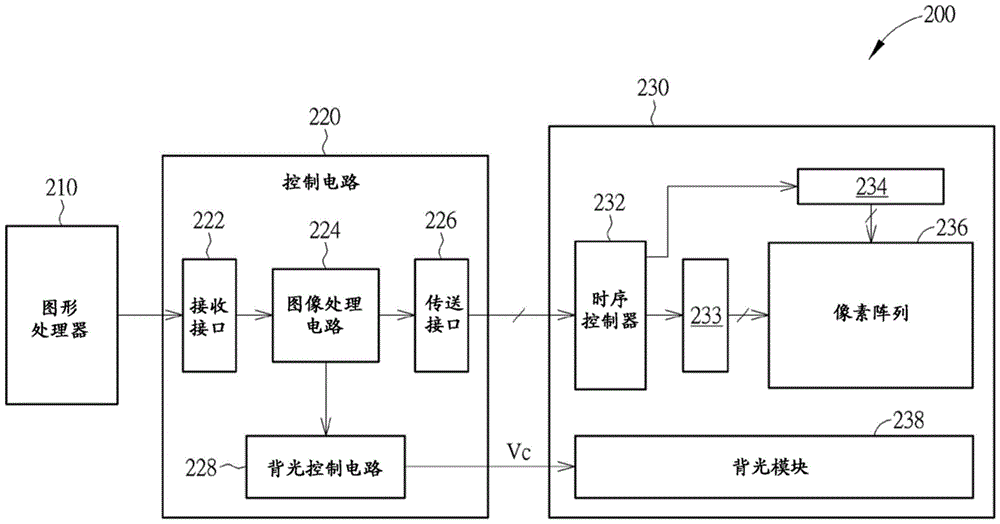
图2为根据本发明实施例的显示器200的示意图。如图2所示,显示器200包含了图形处理器210、控制电路220以及显示面板230。在本实施例中,控制电路220包含了接收接口222、图像处理电路224、传送接口226以及背光控制电路228,其中接收接口222用来接收来自图形处理器210的图像数据后传送至图像处理电路224进行图像处理,而图像处理电路224可以将所接收到的图像数据进行亮度、色彩、或格式上的调整之后产生输出图像数据至传送接口226,以供传送至显示面板230进行显示;此外,背光控制电路228用来产生控制信号Vc以控制显示面板的亮度,其中控制信号Vc可以是脉冲调变(pulse-width modulation,PWM)信号。显示面板230包含了时序控制器232、栅极驱动器233、源驱动器234、像素数组236以及背光模块238,其中时序控制器232接收来自控制电路220的图像数据后产生对应的栅极驱动信号及源驱动信号至栅极驱动器233与源驱动器234,以供控制像素数组236显示出图像画面;此外,背光模块238接收控制信号Vc以显示出对应的亮度。FIG. 2 is a schematic diagram of a
图2所示的显示器200是支持可变更新率(variable refresh rate,VRR)的显示方式,也即控制电路220产生输出图像数据的帧率与图形处理器210产生图像数据的帧率相同。如先前技术中所述,由于显示面板230需要显示的图像的帧率会随着图形处理器210产生图像数据的速度不同而跟着改变,因此,在不同帧率下,像素数组236在电压保持阶段的时间上有很大的差异,造成所显示出的图像亮度/色彩会有差异,进而可能造成画面有闪烁的情形发生。为了解决这个问题,本实施例中提出了一种背光控制方法,其中背光控制电路228可以根据目前所处理的图像帧的帧率,来产生控制信号Vc来动态地调整背光模块238的亮度,以避免图像亮度/色彩不均的问题。The
为了凸显本实施例对于图像亮度/色彩不均的改善,先参考图3所示的先前技术中图像亮度/色彩不均的示意图,其中图3是假设显示面板230为正常黑(normally black)的液晶显示面板,所显现的图像帧F0、F1、F2具有相同的内容,背光亮度维持一致(也即,用来控制背光模块的PWM信号具有固定的工作周期,例如50%),且图像帧F1的帧率比图像帧F0的帧率低(也即,图像帧F1的显示时间比图像帧F0的显示时间长)。在图3中,图像帧F0为垂直同步信号Vsync0至垂直同步信号Vsync1之间的区域、图像帧F1为垂直同步信号Vsync1至垂直同步信号Vsync2之间的区域、图像帧F2为垂直同步信号Vsync2至垂直同步信号Vsync3之间的区域,斜线部分是栅极驱动器233与源驱动器234驱动像素数组236显示出图像画面的时间(可称为主动显示区域),而图像帧的主动显示区域外的区域则为垂直空白间隙,其中主动显示区域前的区域可称为垂直后肩(vertical back porch)区域,而主动显示区域后的区域可称为垂直前肩(vertical front porch)区域。如图3所示,由于图像帧F1的帧率较低,也即具有较长的垂直前肩区域,因此,显示面板230所产生的图像的平均亮度在图像帧F1的垂直前肩区域会因为像素电容具有较长漏电时间而逐渐下降,因此造成图像亮度/色彩不均。In order to highlight the improvement of image brightness/color unevenness in this embodiment, first refer to the schematic diagram of image brightness/color unevenness in the prior art shown in FIG. 3 , wherein FIG. 3 assumes that the
为了解决图3所示的问题,参考图4所示的根据本发明实施例的时序图。如图4所示,背光控制电路228会根据目前图像帧的帧率来决定是否在垂直前肩区域时改变背光模块238的亮度,以补偿图像帧F1因为具有较长的垂直前肩区域所造成的图像的平均亮度下降的问题。具体来说,图像处理电路224在接收到来自图形处理器210的图像数据时,会延迟一段时间后再产生输出图像数据至显示面板230,其中输出图像数据包含了像素数据、垂直同步信号、水平同步信号...等等。而如果图像处理电路224判断图像帧F1具有较低的帧率,例如在一段时间内都未接收到图像帧F2,则背光控制电路228所产生的控制信号Vc,例如PWM信号,会具有较长的工作周期,也即背光模块238在图像帧F1的垂直前肩区域会具有较高的亮度,以使得显示面板230所显示的平均亮度一致。In order to solve the problem shown in FIG. 3 , reference is made to the timing diagram shown in FIG. 4 according to an embodiment of the present invention. As shown in FIG. 4 , the
需注意的是,在图4的实施例中,图像帧F0的主动显示区域及图像帧F1的主动显示区域是对应的相同的背光强度,以维持正常的画面显示。在另一实施例中,图像帧F0的主动显示区域、图像帧F1的主动显示区域、图像帧F0的垂直后肩区域及图像帧F1的垂直后肩区域可以对应的相同的背光强度。It should be noted that, in the embodiment of FIG. 4 , the active display area of the image frame F0 and the active display area of the image frame F1 correspond to the same backlight intensity to maintain normal screen display. In another embodiment, the active display area of the image frame F0, the active display area of the image frame F1, the vertical rear shoulder area of the image frame F0 and the vertical rear shoulder area of the image frame F1 may correspond to the same backlight intensity.
图5所示为先前技术中图像亮度/色彩不均的示意图,其中图5是假设显示面板230为正常白(normally white)的液晶显示面板,所显现的图像帧F0、F1、F2具有相同的内容,背光亮度维持一致,且图像帧F1的帧率比图像帧F0的帧率低。类似以上图3的相关说明,在图5中,由于图像帧F1的帧率较低,也即具有较长的垂直前肩区域,因此,显示面板230所产生的图像的平均亮度在图像帧F1的垂直前肩区域会因为像素电容具有较长漏电时间而逐渐提升,因此造成图像亮度/色彩不均。FIG. 5 is a schematic diagram of image brightness/color unevenness in the prior art, wherein FIG. 5 is a liquid crystal display panel assuming that the
为了解决图5所示的问题,参考图6所示的根据本发明实施例的时序图。如图6所示,背光控制电路228会根据目前图像帧的帧率来决定是否在垂直前肩区域时改变背光模块238的亮度,以补偿图像帧F1因为具有较长的垂直前肩区域所造成的图像的平均亮度下降的问题。具体来说,如果图像处理电路224判断图像帧F1具有较低的帧率,则背光控制电路228所产生的控制信号Vc,例如PWM信号,会具有较低的工作周期,也即背光模块238在图像帧F1的垂直前肩区域会具有较低的亮度,以使得显示面板230所显示的平均亮度一致。In order to solve the problem shown in FIG. 5 , reference is made to the timing diagram according to the embodiment of the present invention shown in FIG. 6 . As shown in FIG. 6 , the
需注意的是,在图6的实施例中,图像帧F0的主动显示区域及图像帧F1的主动显示区域系对应的相同的背光强度,以维持正常的画面显示。在另一实施例中,图像帧F0的主动显示区域、图像帧F1的主动显示区域、图像帧F0的垂直后肩区域及图像帧F1的垂直后肩区域可以对应的相同的背光强度。It should be noted that, in the embodiment of FIG. 6 , the active display area of the image frame F0 and the active display area of the image frame F1 correspond to the same backlight intensity to maintain normal screen display. In another embodiment, the active display area of the image frame F0, the active display area of the image frame F1, the vertical rear shoulder area of the image frame F0 and the vertical rear shoulder area of the image frame F1 may correspond to the same backlight intensity.
图7为根据本发明实施例的显示器700的示意图。如图7所示,显示器700包含了图形处理器710、控制电路720以及显示面板730。在本实施例中,控制电路720包含了接收接口722、图像处理电路724、传送接口726以及背光控制电路728,其中接收接口722用来接收来自图形处理器710的图像数据后传送至图像处理电路724进行图像处理,而图像处理电路724可以将所接收到的图像数据进行亮度、色彩、或格式上的调整之后产生输出图像数据至传送接口726,以供传送至显示面板730进行显示;此外,背光控制电路728用来产生控制信号Vc以控制显示面板的亮度,其中控制信号Vc可以是脉冲调变信号。显示面板730包含了时序控制器732、栅极驱动器733、源驱动器734、像素数组736以及背光模块738,其中时序控制器732接收来自控制电路720的图像数据后产生对应的栅极驱动信号及源驱动信号至栅极驱动器733与源驱动器734,以供控制像素数组736显示出图像画面;此外,背光模块738接收控制信号Vc以显示出对应的亮度。FIG. 7 is a schematic diagram of a
图7所示的显示器700是支持可变更新率的显示方式,也即控制电路720产生输出图像数据的帧率与图形处理器710产生图像数据的帧率相同。如先前技术中所述,由于显示面板730需要显示的图像的帧率会随着图形处理器710产生图像数据的速度不同而跟着改变,因此,在不同帧率下,像素数组736在电压保持阶段的时间上有很大的差异,造成所显示出的图像亮度/色彩会有差异,进而可能造成画面有闪烁的情形发生。为了解决这个问题,本实施例中提出了一种显示控制方法,其中图像处理电路724可以根据目前所处理的图像帧的帧率来调整图像亮度,以避免图像亮度/色彩不均的问题。The
图8为根据本发明的实施例的时序图,其中图8是假设显示面板230为正常黑的液晶显示面板,所显现的图像帧具有相同的内容(例如灰阶图像,例如红色、绿色、蓝色的像素值均为128),背光亮度维持一致(也即,用来控制背光模块的PWM信号具有固定的工作周期)。在图8中,“调整前的平均亮度”指的是先前技术中不采用本实施例的显示控制方法的平均亮度、而“调整后的平均亮度”指的是采用本实施例的显示控制方法的平均亮度。如图8所示,由于图像帧F(0)~F(N-1)具有相同或接近的帧率,因此平均亮度会维持在一个固定值,接着,由于从图像帧F(N)开始帧率下降,因此在图像处理电路724侦测到帧率下降之后,图像处理电路724会在缓冲帧数量之后才开始对图像帧的像素值进行调整,例如提升图像帧F(N+2)的像素值,以使得显示面板230所显示的平均亮度不会具有太大的差异;接着,如果从图像帧F(M)开始帧率提升,因此在图像处理电路724侦测到帧率提升之后,图像处理电路724会在缓冲帧数量之后才开始对图像帧的像素值进行调整,例如将图像帧F(M+2)的像素值设定为原本的像素值。参考图8中“调整前的平均亮度”与“调整后的平均亮度”的变化,本实施例的图像控制方法确实可以改善先前技术中图像亮度/色彩因为帧率变化而不均匀的问题。FIG. 8 is a timing diagram according to an embodiment of the present invention, wherein FIG. 8 is a liquid crystal display panel assuming that the
图9为根据本发明另一实施例的时序图,其中图9是假设显示面板230为正常白的液晶显示面板,所显现的图像帧具有相同的内容(例如灰阶图像,例如红色、绿色、蓝色的像素值均为128),背光亮度维持一致。在图9中,“调整前的平均亮度”指的是先前技术中不采用本实施例的显示控制方法的平均亮度、而“调整后的平均亮度”指的是采用本实施例的显示控制方法的平均亮度。如图9所示,由于图像帧F(0)~F(N-1)具有相同或接近的帧率,因此平均亮度会维持在一个固定值,接着,由于从图像帧F(N)开始帧率下降,因此在图像处理电路724侦测到帧率下降之后,图像处理电路724会在缓冲帧数量之后才开始对图像帧的像素值进行调整,例如降低图像帧F(N+2)的像素值,以使得显示面板230所显示的平均亮度不会具有太大的差异;接着,如果从图像帧F(M)开始帧率提升,因此在图像处理电路724侦测到帧率提升之后,图像处理电路724会在缓冲帧数量之后才开始对图像帧的像素值进行调整,例如将图像帧F(M+2)的像素值设定为原本的像素值。参考图9中“调整前的平均亮度”与“调整后的平均亮度”的变化,本实施例的图像控制方法确实可以改善先前技术中图像亮度/色彩因为帧率变化而不均匀的问题。FIG. 9 is a timing diagram according to another embodiment of the present invention, wherein FIG. 9 is a liquid crystal display panel assuming that the
需注意的是,以上图8、图9所示的实施例仅是作为示例说明,而非是本发明的限制,只要图像处理电路724对具有不同帧率的图像帧使用不同的像素值调整量来进行调整(在此假设具有不同帧率的图像帧具有相同的内容),则相关设计上的变化,例如图像处理电路724对进行像素值调整的缓冲帧数量、像素值调整量的比例、…等等,均应属于本发明的范畴。It should be noted that the above embodiments shown in FIG. 8 and FIG. 9 are only used as examples to illustrate, rather than a limitation of the present invention, as long as the
简要归纳本发明,在本发明的应用于显示器的控制电路中,其可以根据目前所接收的图像数据的帧率来动态地调整背光模块的强度、或是调整图像数据的像素值。通过本发明,可以解决先前技术中因为帧率变动而造成图像画面的亮度/色彩不同的问题,故可以让显示器在帧率变动的情形下维持良好的显示质量。Briefly summarizing the present invention, in the control circuit applied to the display of the present invention, it can dynamically adjust the intensity of the backlight module or adjust the pixel value of the image data according to the frame rate of the currently received image data. The present invention can solve the problem of different brightness/color of images caused by frame rate changes in the prior art, so that the display can maintain good display quality when the frame rate changes.
以上所述仅为本发明的优选实施例,凡依据本发明申请专利范围所做的均等变化与修改,均应属本发明的涵盖范围。The above are only preferred embodiments of the present invention, and all equivalent changes and modifications made according to the scope of the patent application of the present invention shall fall within the scope of the present invention.
【符号说明】【Symbol Description】
200:显示器200: Display
210:图形处理器210: Graphics processor
220:控制电路220: Control circuit
222:接收接口222: Receive interface
224:图像处理电路224: Image Processing Circuits
226:传送接口226: Transmission interface
228:背光控制电路228: Backlight control circuit
230:显示面板230: Display panel
232:时序控制器232: Timing Controller
233:栅极驱动器233: Gate Driver
234:源驱动器234: source drive
236:像素数组236: pixel array
238:背光模块238: Backlight Module
Vc:控制信号Vc: control signal
F0,F1,F2:图像帧F0,F1,F2: Image frame
Vsync0,Vsync1,Vsync2,Vsync3:垂直同步信号Vsync0, Vsync1, Vsync2, Vsync3: vertical sync signal
700:显示器700: Display
710:图形处理器710: Graphics processor
720:控制电路720: Control circuit
722:接收接口722: Receive interface
724:图像处理电路724: Image Processing Circuits
726:传送接口726: Transmission interface
728:背光控制电路728: Backlight Control Circuit
730:显示面板730: Display panel
732:时序控制器732: Timing Controller
733:栅极驱动器733: Gate Drivers
734:源驱动器734: Source drive
736:像素数组736: Pixel array
738:背光模块738: Backlight Module
F(0):图像帧F(0): Image frame
F(N),F(N+1),F(N+2):图像帧F(N), F(N+1), F(N+2): Image frame
F(M),F(M+1),F(M+2):图像帧F(M), F(M+1), F(M+2): Image frame
Claims (10)
Priority Applications (1)
| Application Number | Priority Date | Filing Date | Title |
|---|---|---|---|
| CN202110214280.6A CN114974136A (en) | 2021-02-25 | 2021-02-25 | Control circuit and control method applied to display |
Applications Claiming Priority (1)
| Application Number | Priority Date | Filing Date | Title |
|---|---|---|---|
| CN202110214280.6A CN114974136A (en) | 2021-02-25 | 2021-02-25 | Control circuit and control method applied to display |
Publications (1)
| Publication Number | Publication Date |
|---|---|
| CN114974136A true CN114974136A (en) | 2022-08-30 |
Family
ID=82972728
Family Applications (1)
| Application Number | Title | Priority Date | Filing Date |
|---|---|---|---|
| CN202110214280.6A Pending CN114974136A (en) | 2021-02-25 | 2021-02-25 | Control circuit and control method applied to display |
Country Status (1)
| Country | Link |
|---|---|
| CN (1) | CN114974136A (en) |
Citations (6)
| Publication number | Priority date | Publication date | Assignee | Title |
|---|---|---|---|---|
| CN104299578A (en) * | 2014-11-10 | 2015-01-21 | 深圳市华星光电技术有限公司 | Backlight unit and driving method thereof as well as liquid crystal display device |
| CN105074807A (en) * | 2013-03-13 | 2015-11-18 | 苹果公司 | Compensation methods for display brightness change associated with reduced refresh rate |
| CN106409238A (en) * | 2016-08-30 | 2017-02-15 | 延锋伟世通电子科技(上海)有限公司 | Vehicle display PWM dimming method |
| CN111640390A (en) * | 2020-06-30 | 2020-09-08 | 京东方科技集团股份有限公司 | Display screen flicker adjusting circuit and method and display device |
| CN111833802A (en) * | 2019-04-17 | 2020-10-27 | 三星显示有限公司 | display device |
| US20220262324A1 (en) * | 2021-02-18 | 2022-08-18 | Realtek Semiconductor Corp. | Control circuit applied to display and associated control method |
-
2021
- 2021-02-25 CN CN202110214280.6A patent/CN114974136A/en active Pending
Patent Citations (6)
| Publication number | Priority date | Publication date | Assignee | Title |
|---|---|---|---|---|
| CN105074807A (en) * | 2013-03-13 | 2015-11-18 | 苹果公司 | Compensation methods for display brightness change associated with reduced refresh rate |
| CN104299578A (en) * | 2014-11-10 | 2015-01-21 | 深圳市华星光电技术有限公司 | Backlight unit and driving method thereof as well as liquid crystal display device |
| CN106409238A (en) * | 2016-08-30 | 2017-02-15 | 延锋伟世通电子科技(上海)有限公司 | Vehicle display PWM dimming method |
| CN111833802A (en) * | 2019-04-17 | 2020-10-27 | 三星显示有限公司 | display device |
| CN111640390A (en) * | 2020-06-30 | 2020-09-08 | 京东方科技集团股份有限公司 | Display screen flicker adjusting circuit and method and display device |
| US20220262324A1 (en) * | 2021-02-18 | 2022-08-18 | Realtek Semiconductor Corp. | Control circuit applied to display and associated control method |
Similar Documents
| Publication | Publication Date | Title |
|---|---|---|
| US7839380B2 (en) | Generating corrected gray scale data to improve display quality | |
| EP1376528B1 (en) | Image display and displaying method | |
| US8654060B2 (en) | Processing device and processing method of high dynamic contrast for liquid crystal display apparatus | |
| US11631375B2 (en) | Display equipment and operation method thereof and backlight control device that solves flicker phenomenon of variable refresh rate video frame | |
| US10930248B2 (en) | Display method and display system for reducing a double image effect | |
| US11417288B1 (en) | Control circuit and control method applicable to display panel | |
| KR20150059385A (en) | Method of driving display panel and display apparatus for performing the method | |
| US10930194B2 (en) | Display method and display system for reducing image delay by adjusting an image data clock signal | |
| WO2022141567A1 (en) | Display panel and electronic device | |
| CN101241676B (en) | Method and display device for displaying image data capable of improving double boundary problem | |
| KR20220147880A (en) | Display device and operating method thereof | |
| CN114023238B (en) | Display device | |
| TWI779494B (en) | Control circuit and control method applied to display | |
| CN113674664B (en) | White balance adjusting method of display device and display device | |
| CN111326125A (en) | TCON time sequence control signal control method and driving circuit | |
| CN105719604B (en) | Method for improving panel automatic updating picture flicker of display panel and control circuit thereof | |
| CN114974136A (en) | Control circuit and control method applied to display | |
| KR100577300B1 (en) | Driving Method of LCD | |
| CN118248058A (en) | Display method, timing controller and display device | |
| CN114974149B (en) | Control circuit and control method applied to display panel | |
| JP4910356B2 (en) | Liquid crystal display | |
| TWI698851B (en) | Display method for reducing image delay and display system | |
| JP2008051912A (en) | Liquid crystal display | |
| CN115440154A (en) | Display panel drive circuit | |
| WO2023024135A1 (en) | Driving circuit and display device |
Legal Events
| Date | Code | Title | Description |
|---|---|---|---|
| PB01 | Publication | ||
| PB01 | Publication | ||
| SE01 | Entry into force of request for substantive examination | ||
| SE01 | Entry into force of request for substantive examination |