CN114745854A - Drilling method of PCB board - Google Patents
Drilling method of PCB board Download PDFInfo
- Publication number
- CN114745854A CN114745854A CN202210360145.7A CN202210360145A CN114745854A CN 114745854 A CN114745854 A CN 114745854A CN 202210360145 A CN202210360145 A CN 202210360145A CN 114745854 A CN114745854 A CN 114745854A
- Authority
- CN
- China
- Prior art keywords
- pcb board
- drilling
- drilled
- circular hole
- target
- Prior art date
- Legal status (The legal status is an assumption and is not a legal conclusion. Google has not performed a legal analysis and makes no representation as to the accuracy of the status listed.)
- Pending
Links
- 238000005553 drilling Methods 0.000 title claims abstract description 71
- 238000000034 method Methods 0.000 title claims abstract description 38
- 238000005520 cutting process Methods 0.000 description 8
- 230000000694 effects Effects 0.000 description 4
- 238000010586 diagram Methods 0.000 description 3
- 238000009825 accumulation Methods 0.000 description 2
- 239000000463 material Substances 0.000 description 2
- 230000002028 premature Effects 0.000 description 2
- 229920000877 Melamine resin Polymers 0.000 description 1
- 229920002522 Wood fibre Polymers 0.000 description 1
- 230000002159 abnormal effect Effects 0.000 description 1
- 230000005856 abnormality Effects 0.000 description 1
- XAGFODPZIPBFFR-UHFFFAOYSA-N aluminium Chemical compound [Al] XAGFODPZIPBFFR-UHFFFAOYSA-N 0.000 description 1
- 229910052782 aluminium Inorganic materials 0.000 description 1
- 230000009286 beneficial effect Effects 0.000 description 1
- 238000004140 cleaning Methods 0.000 description 1
- 239000004020 conductor Substances 0.000 description 1
- 238000009826 distribution Methods 0.000 description 1
- 238000005530 etching Methods 0.000 description 1
- 238000012423 maintenance Methods 0.000 description 1
- 238000004519 manufacturing process Methods 0.000 description 1
- JDSHMPZPIAZGSV-UHFFFAOYSA-N melamine Chemical compound NC1=NC(N)=NC(N)=N1 JDSHMPZPIAZGSV-UHFFFAOYSA-N 0.000 description 1
- ISWSIDIOOBJBQZ-UHFFFAOYSA-N phenol group Chemical group C1(=CC=CC=C1)O ISWSIDIOOBJBQZ-UHFFFAOYSA-N 0.000 description 1
- 238000004801 process automation Methods 0.000 description 1
- 239000000126 substance Substances 0.000 description 1
- 238000005406 washing Methods 0.000 description 1
- 239000002025 wood fiber Substances 0.000 description 1
Images


Classifications
-
- H—ELECTRICITY
- H05—ELECTRIC TECHNIQUES NOT OTHERWISE PROVIDED FOR
- H05K—PRINTED CIRCUITS; CASINGS OR CONSTRUCTIONAL DETAILS OF ELECTRIC APPARATUS; MANUFACTURE OF ASSEMBLAGES OF ELECTRICAL COMPONENTS
- H05K3/00—Apparatus or processes for manufacturing printed circuits
- H05K3/0011—Working of insulating substrates or insulating layers
- H05K3/0044—Mechanical working of the substrate, e.g. drilling or punching
- H05K3/0047—Drilling of holes
Landscapes
- Engineering & Computer Science (AREA)
- Manufacturing & Machinery (AREA)
- Microelectronics & Electronic Packaging (AREA)
- Perforating, Stamping-Out Or Severing By Means Other Than Cutting (AREA)
Abstract
本发明实施例提供一种PCB板的钻孔方法,在待钻孔的PCB板底面垫设垫板;在目标圆孔的区域范围钻孔成型出至少三个圆心沿所述目标圆孔的一个同心圆的圆周线均匀分布的预钻圆孔,相邻的预钻圆孔的圆心距大于相应的两个预钻圆孔的半径之和,同心圆与目标圆孔的圆周线的间距大于任意一个预钻圆孔的半径,预钻圆孔的深度为钻穿所述PCB板并钻至垫板内第一预定深度;以及按照在所述PCB板中的钻入深度分别达到厚度的预定的N等分点时即先抬刀退出再重新进入实施钻孔的方式分多段钻穿所述PCB板,且在钻穿PCB板后不抬刀而继续钻入垫板内第二预定深度即成型出所述目标圆孔,所述第二预定深度大于所述第一预定深度。本发明实施例能减少钻孔切口毛刺,提高钻孔质量。
An embodiment of the present invention provides a method for drilling a PCB board. A backing plate is placed on the bottom surface of the PCB board to be drilled; and one of at least three circular holes centered along the target circular hole is formed by drilling in the area of the target circular hole. Pre-drilled circular holes with evenly distributed circumferences of concentric circles, the center-to-center distance of adjacent pre-drilled circular holes is greater than the sum of the radii of the corresponding two pre-drilled circular holes, and the distance between the concentric circles and the circumference of the target circular hole is greater than any The radius of a pre-drilled circular hole, the depth of the pre-drilled circular hole is to drill through the PCB board and drill to the first predetermined depth in the backing plate; At the N equal point, lift the knife to exit and then re-enter the drilling method to drill through the PCB board in multiple sections, and after drilling through the PCB board, do not lift the knife and continue to drill into the backing plate to a second predetermined depth, that is, forming The target circular hole is drawn out, and the second predetermined depth is greater than the first predetermined depth. The embodiment of the present invention can reduce the burr of the drilling incision and improve the drilling quality.
Description
技术领域technical field
本发明实施例涉及PCB板加工技术领域,尤其涉及一种PCB板的钻孔方法。Embodiments of the present invention relate to the technical field of PCB board processing, and in particular, to a method for drilling a PCB board.
背景技术Background technique
钻孔是PCB板加工的一个重要环节,尤其是在钻孔径为4.00mm以上的大孔时,钻孔过程中切削阻力大,切割过程不顺畅,切口边缘处会产生毛刺,所制得的孔很难达到行业标准。通常的处理方法是采用额外的流程或工艺,通过机械打磨、高压冲洗、化学微蚀等方式去除已经产生的毛刺,由此得到符合要求的孔,工艺流程复杂,且生产效率低。Drilling is an important part of PCB processing, especially when drilling large holes with a diameter of more than 4.00mm, the cutting resistance is large during the drilling process, the cutting process is not smooth, and burrs will be generated at the edge of the incision. The holes are difficult to meet industry standards. The usual treatment method is to use an additional process or process to remove the generated burrs through mechanical grinding, high-pressure washing, chemical micro-etching, etc., so as to obtain holes that meet the requirements. The process is complicated and the production efficiency is low.
发明内容SUMMARY OF THE INVENTION
本发明实施例要解决的技术问题在于,提供一种PCB板的钻孔方法,减少钻孔切口毛刺,提高钻孔质量。The technical problem to be solved by the embodiments of the present invention is to provide a drilling method for a PCB board, which can reduce the burr of the drilling incision and improve the drilling quality.
为了解决上述技术问题,本发明实施例提供以下技术方案:一种PCB板的钻孔方法,包括以下步骤:In order to solve the above technical problems, the embodiments of the present invention provide the following technical solutions: a method for drilling a PCB board, comprising the following steps:
在待钻孔的PCB板底面垫设垫板;A pad is placed on the bottom of the PCB to be drilled;
在所述PCB板上预定的用于成型目标圆孔的区域范围钻孔成型出至少三个圆心沿所述目标圆孔的一个同心圆的圆周线均匀分布的预钻圆孔,任意两个相邻的所述预钻圆孔的圆心距大于相应的两个所述预钻圆孔的半径之和,所述同心圆与所述目标圆孔的圆周线的间距大于任意一个所述预钻圆孔的半径,所述预钻圆孔的深度为钻穿所述PCB板并钻入所述垫板内第一预定深度;以及At least three pre-drilled circular holes whose centers are evenly distributed along the circumference of a concentric circle of the target circular hole are drilled in the predetermined area of the PCB board for forming the target circular hole. The center-to-center distance of the adjacent pre-drilled circular holes is greater than the sum of the radii of the corresponding two pre-drilled circular holes, and the distance between the concentric circle and the circumference of the target circular hole is greater than any one of the pre-drilled circles The radius of the hole, the depth of the pre-drilled circular hole is a first predetermined depth drilled through the PCB board and into the backing plate; and
根据所述PCB板的厚度,按照在所述PCB板中的钻入深度分别达到所述PCB板厚度的预定的N等分点时即先抬刀退出再重新进入实施钻孔的方式分多段钻穿所述PCB板,且在钻穿所述PCB板后不抬刀而继续钻入所述垫板内第二预定深度即成型出所述目标圆孔,所述第二预定深度大于所述第一预定深度,N大于或等于2。According to the thickness of the PCB board, when the drilling depth in the PCB board reaches the predetermined N equal points of the thickness of the PCB board, that is, first lift the knife to exit and then re-enter the drilling method to drill in multiple sections. Through the PCB board, and after drilling through the PCB board, the knife is not lifted but continues to drill into the backing plate to a second predetermined depth to form the target circular hole, and the second predetermined depth is greater than the first predetermined depth. A predetermined depth, where N is greater than or equal to 2.
进一步地,各个所述预钻圆孔的直径相同。Further, each of the pre-drilled circular holes has the same diameter.
进一步地,所述预钻圆孔的数量为四个,位于对角的两个所述预钻圆孔的间距不小于1.5mm,所述同心圆与所述目标圆孔的圆周线的间距与所述预钻圆孔的半径的差值不小于0.1mm。Further, the number of the pre-drilled circular holes is four, the distance between the two pre-drilled circular holes located at the opposite corners is not less than 1.5mm, and the distance between the concentric circle and the circumference of the target circular hole is the same as that of the target circular hole. The difference between the radii of the pre-drilled circular holes is not less than 0.1 mm.
进一步地,所述目标圆孔直径D与预钻圆孔直径d满足以下关系:d=(D-1.7032)/2。Further, the target circular hole diameter D and the pre-drilled circular hole diameter d satisfy the following relationship: d=(D-1.7032)/2.
进一步地,所述第一预定深度为所述垫板厚度的15%-30%。Further, the first predetermined depth is 15%-30% of the thickness of the backing plate.
进一步地,所述第二预定深度为所述垫板厚度的25%-50%。Further, the second predetermined depth is 25%-50% of the thickness of the backing plate.
进一步地,在钻取所述目标圆孔时,钻咀在所述目标圆孔的圆心处下刀。Further, when drilling the target circular hole, the drill tip is cut at the center of the target circular hole.
进一步地,所述PCB板固定放置在具有坐标系的基台上,通过坐标系相应数据确定所述PCB板上成型所述预钻圆孔以及所述目标圆孔的位置进而控制用于钻孔的钻咀在所述坐标系内精准移动至需钻孔的位置处实施钻孔。Further, the PCB board is fixedly placed on a base with a coordinate system, and the position of the pre-drilled circular hole and the target circular hole formed on the PCB board is determined by the corresponding data of the coordinate system to control the drilling for drilling. The drill bit is precisely moved to the position to be drilled in the coordinate system to perform drilling.
进一步地,所述待钻孔的PCB板顶面还贴设有盖板。Further, a cover plate is attached to the top surface of the PCB to be drilled.
进一步地,所述盖板与所述垫板均通过定位钉与所述PCB板相对固定。Further, both the cover plate and the backing plate are relatively fixed to the PCB board through positioning pins.
采用上述技术方案后,本发明实施例至少具有如下有益效果:本发明实施例通过在待钻孔的PCB板底面垫设垫板,并在钻取目标圆孔之前,先在成型所述目标圆孔的区域范围内成型出三个以上预钻圆孔以降低切割量,减小后续成型所述目标圆孔时的板面阻力;且所述预钻圆孔沿所述目标圆孔的一个同心圆的圆周线均匀分布,各方向上减阻效果均匀,最大程度减小毛刺产生的可能,且任意两个相邻的所述预钻圆孔的圆心距大于相应的两个所述预钻圆孔的半径之和,间距合理,降低成型预钻圆孔的操作难度,所述同心圆与所述目标圆孔的圆周线的间距大于任意一个所述预钻圆孔的半径,避免影响目标圆孔的真圆率,选用直径与预钻圆孔的直径相匹配的钻咀,钻穿所述PCB板后钻入所述垫板内第一预定深度即可成型出预钻圆孔,操作相对简单。另外,根据所述PCB板的厚度,按照在所述PCB板中的钻入深度分别达到所述PCB板厚度的预定的N(N≥2)等分点时即先抬刀退出再重新进入实施钻孔的方式分多段钻穿所述PCB板,便于适时调整和控制钻孔方向和钻咀状态,避免误差积累造成目标圆孔孔型异常,且在钻穿所述PCB板后不抬刀而继续钻入所述垫板内第二预定深度即成型出所述目标圆孔,避免抬刀过早产生毛刺,同时垫板还能对钻咀起到一定清洁作用,方便带走钻咀上的钻屑,提升钻孔效率。After the above technical solution is adopted, the embodiment of the present invention has at least the following beneficial effects: the embodiment of the present invention uses a pad on the bottom surface of the PCB board to be drilled, and before drilling the target circular hole, the target circle is formed first. More than three pre-drilled circular holes are formed within the area of the hole to reduce the cutting amount and reduce the board surface resistance when the target circular hole is subsequently formed; and the pre-drilled circular hole is along a concentric point of the target circular hole. The circumference of the circle is evenly distributed, the drag reduction effect is uniform in all directions, and the possibility of burrs is minimized, and the center-to-center distance of any two adjacent pre-drilled circular holes is greater than the corresponding two pre-drilled circles The sum of the radii of the holes has a reasonable spacing, which reduces the difficulty of forming pre-drilled circular holes. The distance between the concentric circle and the circumference of the target circular hole is greater than the radius of any one of the pre-drilled circular holes to avoid affecting the target circle. The true circularity of the hole, select the drill nozzle whose diameter matches the diameter of the pre-drilled circular hole, drill through the PCB board and then drill into the first predetermined depth in the backing plate to form the pre-drilled circular hole. The operation is relatively Simple. In addition, according to the thickness of the PCB board, when the drilling depth in the PCB board reaches the predetermined N (N≥2) bisector point of the thickness of the PCB board, the knife is lifted first and then exits and then re-enters the implementation. The drilling method drills through the PCB board in multiple sections, which is convenient to adjust and control the drilling direction and the state of the drill nozzle in time, avoid the accumulation of errors and cause abnormal hole shape of the target round hole, and do not lift the knife after drilling through the PCB board. Continue to drill into the second predetermined depth in the backing plate to form the target round hole, so as to avoid premature burrs when the knife is lifted. Drilling cuttings, improve drilling efficiency.
附图说明Description of drawings
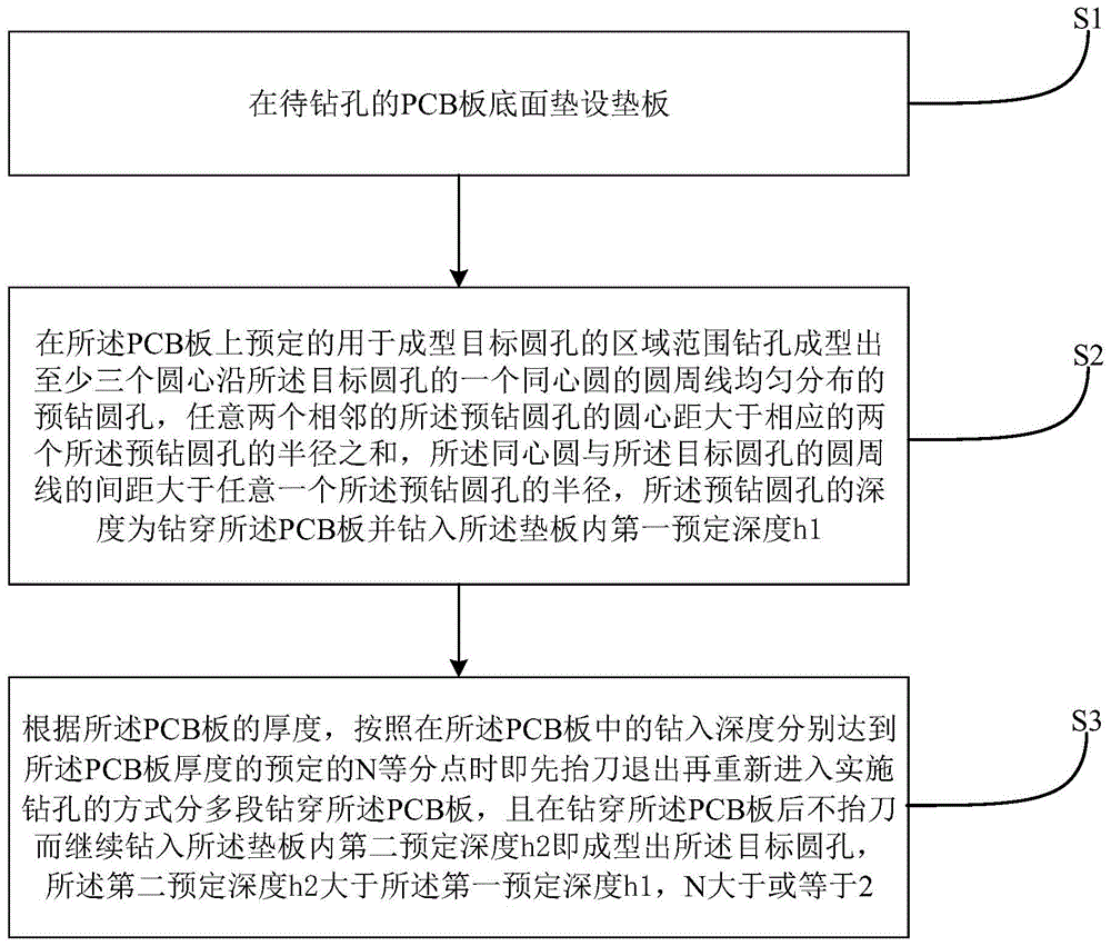
图1为本发明PCB板的钻孔方法一个可选实施例的步骤流程示意图。FIG. 1 is a schematic flow chart of steps of an optional embodiment of a method for drilling a PCB board according to the present invention.
图2为本发明PCB板的钻孔方法一个可选实施例的目标圆孔与预钻圆孔位置分布示意图。FIG. 2 is a schematic diagram of the position distribution of target circular holes and pre-drilled circular holes in an optional embodiment of the method for drilling a PCB board according to the present invention.
图3为本发明PCB板的钻孔方法一个可选实施例的所述盖板、PCB板及垫板的结构示意图。FIG. 3 is a schematic structural diagram of the cover plate, the PCB board and the backing plate according to an alternative embodiment of the method for drilling a PCB board according to the present invention.
图4为本发明PCB板的钻孔方法一个可选实施例的分步钻孔示意图。FIG. 4 is a schematic diagram of step-by-step drilling of an optional embodiment of the method for drilling a PCB board according to the present invention.
具体实施方式Detailed ways
下面结合附图和具体实施例对本申请作进一步详细说明。应当理解,以下的示意性实施例及说明仅用来解释本发明,并不作为对本发明的限定,而且,在不冲突的情况下,本申请中的实施例及实施例中的特征可以相互结合。The present application will be further described in detail below with reference to the accompanying drawings and specific embodiments. It should be understood that the following exemplary embodiments and descriptions are only used to explain the present invention, but not to limit the present invention, and, in the case of no conflict, the embodiments in the present application and the features in the embodiments can be combined with each other .
如图1-图4所示,本发明一个可选实施例提供一种PCB板的钻孔方法,包括以下步骤:As shown in FIG. 1-FIG. 4, an optional embodiment of the present invention provides a method for drilling a PCB board, including the following steps:
S1:在待钻孔的PCB板1底面垫设垫板2;S1: A
S2:在所述PCB板1上预定的用于成型目标圆孔4的区域范围钻孔成型出至少三个圆心沿所述目标圆孔4的一个同心圆6的圆周线均匀分布的预钻圆孔5,任意两个相邻的所述预钻圆孔5的圆心距大于相应的两个所述预钻圆孔5的半径之和,所述同心圆6与所述目标圆孔4的圆周线的间距大于任意一个所述预钻圆孔5的半径,所述预钻圆孔5的深度为钻穿所述PCB板1并钻入所述垫板2内第一预定深度h1;以及S2: Drill holes in the predetermined area of the PCB board 1 for forming the target
S3:根据所述PCB板1的厚度,按照在所述PCB板1中的钻入深度分别达到所述PCB板1厚度的预定的N等分点时即先抬刀退出再重新进入实施钻孔的方式分多段钻穿所述PCB板1,且在钻穿所述PCB板1后不抬刀而继续钻入所述垫板2内第二预定深度h2即成型出所述目标圆孔5,所述第二预定深度h2大于所述第一预定深度h1,N大于或等于2。S3: According to the thickness of the PCB board 1, when the drilling depth in the PCB board 1 reaches the predetermined N equal points of the thickness of the PCB board 1 respectively, lift the knife to exit and then re-enter the drilling process The method is to drill through the PCB board 1 in multiple sections, and after drilling through the PCB board 1, the
本发明实施例通过在待钻孔的PCB板1底面垫设垫板2,并在钻取目标圆孔4之前,先在成型所述目标圆孔4的区域范围内成型出三个以上预钻圆孔5以降低切割量,减小后续成型所述目标圆孔4时的板面阻力;且所述预钻圆孔5沿所述目标圆孔4的一个同心圆6的圆周线均匀分布,各方向上减阻效果均匀,最大程度减小毛刺产生的可能,且任意两个相邻的所述预钻圆孔5的圆心距大于相应的两个所述预钻圆孔5的半径之和,间距合理,降低成型预钻圆孔5的操作难度,所述同心圆6与所述目标圆孔4的圆周线的间距大于任意一个所述预钻圆孔5的半径,避免影响目标圆孔4的真圆率,选用直径与预钻圆孔5的直径相匹配的钻咀,钻穿所述PCB板1后钻入所述垫板2内第一预定深度h1即可成型出预钻圆孔5,操作相对简单。另外,根据所述PCB板1的厚度,按照在所述PCB板1中的钻入深度分别达到所述PCB板1厚度的预定的N(N≥2)等分点时即先抬刀退出再重新进入实施钻孔的方式分多段钻穿所述PCB板1,便于适时调整和控制钻孔方向和钻咀状态,避免误差积累造成目标圆孔孔型异常,且在钻穿所述PCB板1后不抬刀而继续钻入所述垫板2内第二预定深度h2即成型出所述目标圆孔4,避免抬刀过早产生毛刺,同时垫板2还能对钻咀起到一定清洁作用,方便带走钻咀上的钻屑,提升钻孔效率。在具体实施过程中,市面上常见的钻咀直径尺寸梯度为0.05mm,因此预钻圆孔5实际钻孔的直径与预设值之间的误差不超过0.05mm;以常见的2.4mm厚度的FR4材料制成的PCB板1为例,N优选为3,每次钻0.8mm,第三次下刀钻穿所述PCB板1后钻入垫板2内直至第一预定深度h1,所述垫板2可采用高密度木质纤维板、密胺板或酚酫板,经济实惠,方便控制成本。In the embodiment of the present invention, a
在本发明一个可选实施例中,如图2所示,各个所述预钻圆孔5的直径相同。本实施例通过将预钻圆孔5设为直径相同的至少三个沿所述目标圆孔4的一个同心圆6的圆周线均匀分布,进一步简化成型操作。In an optional embodiment of the present invention, as shown in FIG. 2 , each of the pre-drilled
在本发明一个可选实施例中,如图2所示,所述预钻圆孔5的数量为四个,位于对角的两个所述预钻圆孔5的间距不小于1.5mm,所述同心圆6与所述目标圆孔的圆周线的间距与所述预钻圆孔5的半径的差值不小于0.1mm。本实施例通过将预钻圆孔数量设置为4个,兼顾钻孔效率与预切割量的多少,减小精度要求,操作相对简便,保证减阻效果;且位于对角的两个所述预钻圆孔5的间距不小于1.5mm,间距合理,降低钻取预钻圆孔5的操作难度,且所述同心圆6与所述目标圆孔4的圆周线的间距与所述预钻圆孔5的半径的差值不小于0.1mm,保留0.1mm以上的钻孔容错范围,提高目标圆孔4的真圆率。In an optional embodiment of the present invention, as shown in FIG. 2 , the number of the pre-drilled
在本发明一个可选实施例中,如图2所示,所述目标圆孔直径D与预钻圆孔直径d满足以下关系:d=(D-1.7032)/2。本实施例通过计算公式d=(D-1.7032)/2来确定目标圆孔4直径D与预钻圆孔5直径d,便于对应不同直径大小的目标圆孔4灵活得出不同钻孔方案。在具体实施过程中,计算得出的预钻圆孔5直径d保留两位小数,并选用直径与所述计算值最接近的钻咀钻取所述预钻圆孔5。In an optional embodiment of the present invention, as shown in FIG. 2 , the target circular hole diameter D and the pre-drilled circular hole diameter d satisfy the following relationship: d=(D-1.7032)/2. In this embodiment, the diameter D of the target
在本发明一个可选实施例中,如图4所示,所述第一预定深度h1为所述垫板2厚度的15%-30%。本实施例通过选用直径与所述预钻圆孔5直径d最接近的钻咀在所述目标圆孔4内钻至所述垫板2厚度的15%-30%,而获得若干个所述预钻圆孔5,所述垫板2对钻咀起到一定清洁作用,带走钻咀上的钻屑。In an optional embodiment of the present invention, as shown in FIG. 4 , the first predetermined depth h1 is 15%-30% of the thickness of the
在本发明一个可选实施例中,如图4所示,所述第二预定深度h2为所述垫板2厚度的25%-50%。本实施例通过在钻取所述目标圆孔4时,分段钻切钻穿所述PCB板1后钻入所述垫板2厚度的25%-50%,足够清理钻咀上的钻屑,便于钻咀的后续养护,同时不影响垫板2的双面使用,提高垫板2利用率。In an optional embodiment of the present invention, as shown in FIG. 4 , the second predetermined depth h2 is 25%-50% of the thickness of the
在本发明一个可选实施例中,如图2所示,在钻取所述目标圆孔4时,钻咀在所述目标圆孔4的圆心处下刀。本实施例通过以所述预钻圆孔5圆心处作为下钻落刀点,对落刀精准度要求小,便于操作。In an optional embodiment of the present invention, as shown in FIG. 2 , when drilling the target
在本发明一个可选实施例中,所述PCB板1固定放置在具有坐标系的基台上,通过坐标系相应数据确定所述PCB板1上成型所述预钻圆孔5以及所述目标圆孔4的位置进而控制用于钻孔的钻咀在所述坐标系内精准移动至需钻孔的位置处实施钻孔。本实施例通过将所述PCB板1固定放置在具有坐标系的基台上,以坐标系相应数据来确定所述预钻圆孔5以及所述目标圆孔4的位置,便于精准定位,外部接入其他设备可进一步提升工艺自动化程度,减少人工成本和操作误差。In an optional embodiment of the present invention, the PCB board 1 is fixedly placed on a base with a coordinate system, and the pre-drilled
在本发明一个可选实施例中,如图3所示,所述待钻孔的PCB板1顶面还贴设有盖板3。本实施例通过在PCB板1顶面贴设有盖板3,可以理解的是在具体实施过程中,所述盖板3可以选用0.13mm-0.18mm厚度的冷冲板或铝片等硬度低的材料板,方便在下钻时快速定位,使钻孔位置偏差更小,同时所述盖板3还是热的良好导体,能为所述钻咀散热,提高钻孔效率。In an optional embodiment of the present invention, as shown in FIG. 3 , a
在本发明一个可选实施例中,所述盖板3与所述垫板2均通过定位钉与所述PCB板1相对固定。本实施例通过定位钉将所述盖板3、所述垫板2固定至所述PCB板1上,操作简单,组合固定与拆分都很方便。In an optional embodiment of the present invention, both the
上面结合附图对本发明的实施例进行了描述,但是本发明并不局限于上述的具体实施方式,上述的具体实施方式仅仅是示意性的,而不是限制性的,本领域的普通技术人员在本发明的启示下,在不脱离本发明宗旨和权利要求所保护的范围情况下,还可做出很多形式,这些均属于本发明的保护范围之内。The embodiments of the present invention have been described above in conjunction with the accompanying drawings, but the present invention is not limited to the above-mentioned specific embodiments, which are merely illustrative rather than restrictive. Under the inspiration of the present invention, without departing from the scope of protection of the spirit of the present invention and the claims, many forms can be made, which all fall within the protection scope of the present invention.
Claims (10)
Priority Applications (1)
| Application Number | Priority Date | Filing Date | Title |
|---|---|---|---|
| CN202210360145.7A CN114745854A (en) | 2022-04-07 | 2022-04-07 | Drilling method of PCB board |
Applications Claiming Priority (1)
| Application Number | Priority Date | Filing Date | Title |
|---|---|---|---|
| CN202210360145.7A CN114745854A (en) | 2022-04-07 | 2022-04-07 | Drilling method of PCB board |
Publications (1)
| Publication Number | Publication Date |
|---|---|
| CN114745854A true CN114745854A (en) | 2022-07-12 |
Family
ID=82279960
Family Applications (1)
| Application Number | Title | Priority Date | Filing Date |
|---|---|---|---|
| CN202210360145.7A Pending CN114745854A (en) | 2022-04-07 | 2022-04-07 | Drilling method of PCB board |
Country Status (1)
| Country | Link |
|---|---|
| CN (1) | CN114745854A (en) |
Cited By (2)
| Publication number | Priority date | Publication date | Assignee | Title |
|---|---|---|---|---|
| CN117082742A (en) * | 2023-08-22 | 2023-11-17 | 阔智通测科技(广州)有限公司 | Drilling equipment for printed circuit board and processing technology thereof |
| CN119789324A (en) * | 2025-03-07 | 2025-04-08 | 南京大量数控科技有限公司 | Drilling equipment and drilling method |
Citations (8)
| Publication number | Priority date | Publication date | Assignee | Title |
|---|---|---|---|---|
| CN1500234A (en) * | 2001-01-09 | 2004-05-26 | Զ���� | incremental step drilling system and method |
| CN204425769U (en) * | 2014-12-24 | 2015-06-24 | 特新微电子(东莞)有限公司 | A circuit board pre-drilled hole structure |
| CN105163493A (en) * | 2015-07-09 | 2015-12-16 | 高德(无锡)电子有限公司 | Laminated boring technology for combined soft and hard printed circuit boards |
| CN205029957U (en) * | 2015-09-24 | 2016-02-10 | 广州兴森快捷电路科技有限公司 | Drilling structure of lamination board |
| CN108770209A (en) * | 2018-07-10 | 2018-11-06 | 江西旭昇电子有限公司 | The forming method of printed wiring board profiled holes |
| CN109922603A (en) * | 2019-04-18 | 2019-06-21 | 生益电子股份有限公司 | PCB drilling method |
| CN110191585A (en) * | 2019-05-30 | 2019-08-30 | 广合科技(广州)有限公司 | Big-diameter hole drilling is without the method for pulling copper in a kind of PCB |
| CN113141717A (en) * | 2021-04-21 | 2021-07-20 | 丰顺县和生电子有限公司 | Drilling method of circuit board motherboard |
-
2022
- 2022-04-07 CN CN202210360145.7A patent/CN114745854A/en active Pending
Patent Citations (8)
| Publication number | Priority date | Publication date | Assignee | Title |
|---|---|---|---|---|
| CN1500234A (en) * | 2001-01-09 | 2004-05-26 | Զ���� | incremental step drilling system and method |
| CN204425769U (en) * | 2014-12-24 | 2015-06-24 | 特新微电子(东莞)有限公司 | A circuit board pre-drilled hole structure |
| CN105163493A (en) * | 2015-07-09 | 2015-12-16 | 高德(无锡)电子有限公司 | Laminated boring technology for combined soft and hard printed circuit boards |
| CN205029957U (en) * | 2015-09-24 | 2016-02-10 | 广州兴森快捷电路科技有限公司 | Drilling structure of lamination board |
| CN108770209A (en) * | 2018-07-10 | 2018-11-06 | 江西旭昇电子有限公司 | The forming method of printed wiring board profiled holes |
| CN109922603A (en) * | 2019-04-18 | 2019-06-21 | 生益电子股份有限公司 | PCB drilling method |
| CN110191585A (en) * | 2019-05-30 | 2019-08-30 | 广合科技(广州)有限公司 | Big-diameter hole drilling is without the method for pulling copper in a kind of PCB |
| CN113141717A (en) * | 2021-04-21 | 2021-07-20 | 丰顺县和生电子有限公司 | Drilling method of circuit board motherboard |
Cited By (4)
| Publication number | Priority date | Publication date | Assignee | Title |
|---|---|---|---|---|
| CN117082742A (en) * | 2023-08-22 | 2023-11-17 | 阔智通测科技(广州)有限公司 | Drilling equipment for printed circuit board and processing technology thereof |
| CN117082742B (en) * | 2023-08-22 | 2024-05-28 | 阔智通测科技(广州)有限公司 | Drilling equipment for printed circuit board and processing technology thereof |
| CN119789324A (en) * | 2025-03-07 | 2025-04-08 | 南京大量数控科技有限公司 | Drilling equipment and drilling method |
| CN119789324B (en) * | 2025-03-07 | 2025-07-08 | 南京大量数控科技有限公司 | Drilling equipment and drilling method |
Similar Documents
| Publication | Publication Date | Title |
|---|---|---|
| CN114745854A (en) | Drilling method of PCB board | |
| CN103170995B (en) | Manufacture method of short slotted hole for printed circuit board | |
| CN102510667B (en) | CNC (Computer Numerical Control) board splitting production method without NPTH (Non Plating Through Hole) hole positioning | |
| WO2015109908A1 (en) | Drilling method for pcbs with high hole position precision | |
| CN112770512B (en) | A kind of PCB board short slot hole processing method and processing device | |
| CN104493349A (en) | Plasma small hole cutting machining method | |
| CN103111650A (en) | Processing method for drilling of numerical control milling machine capable of inclining main shaft | |
| CN203253962U (en) | Full-automatic drilling machine | |
| CN114953033B (en) | Method for mechanically drilling through hole with high aspect ratio | |
| CN108449879B (en) | Back-drilling method of PCB | |
| CN105307396A (en) | Manufacturing method of PCB with square holes | |
| CN106425592A (en) | Clamp and method for even deburring for oblique wall drilling | |
| CN116056338A (en) | Secondary positioning processing technology for routing slot of printed circuit board | |
| CN110744267B (en) | Ring for wind power equipment and machining process | |
| CN107486892A (en) | PCB board drilling positioning method | |
| CN115915616A (en) | Novel method for drilling aluminum substrate | |
| CN114952366A (en) | Drilling method of circuit board motherboard | |
| CN106142205A (en) | Diameter 0.25mm following printed wiring board finished hole processing method | |
| CN205254163U (en) | Process drilling machine in rigid circuit card slot hole | |
| CN207678080U (en) | A kind of PCB circuit board pore-forming positioning plate | |
| CN205660197U (en) | Tool is supported in drilling of iron fluorine dragon PCB board | |
| CN204968247U (en) | Two bore or gong limit pin positioner | |
| CN206952187U (en) | A machining tool for square grooves on inner holes of inner circles | |
| CN114867205B (en) | A short slot hole drilling process for PCB board | |
| CN207564057U (en) | A kind of camshaft punching machine typewriting fixture |
Legal Events
| Date | Code | Title | Description |
|---|---|---|---|
| PB01 | Publication | ||
| PB01 | Publication | ||
| SE01 | Entry into force of request for substantive examination | ||
| SE01 | Entry into force of request for substantive examination | ||
| RJ01 | Rejection of invention patent application after publication | ||
| RJ01 | Rejection of invention patent application after publication |
Application publication date: 20220712 |