CN114582962B - Variable channel AlGaN/GaN HEMT structure and preparation method thereof - Google Patents
Variable channel AlGaN/GaN HEMT structure and preparation method thereof Download PDFInfo
- Publication number
- CN114582962B CN114582962B CN202210462372.0A CN202210462372A CN114582962B CN 114582962 B CN114582962 B CN 114582962B CN 202210462372 A CN202210462372 A CN 202210462372A CN 114582962 B CN114582962 B CN 114582962B
- Authority
- CN
- China
- Prior art keywords
- gan
- algan
- layer
- groove
- passivation layer
- Prior art date
- Legal status (The legal status is an assumption and is not a legal conclusion. Google has not performed a legal analysis and makes no representation as to the accuracy of the status listed.)
- Active
Links
Images


Classifications
-
- H—ELECTRICITY
- H10—SEMICONDUCTOR DEVICES; ELECTRIC SOLID-STATE DEVICES NOT OTHERWISE PROVIDED FOR
- H10D—INORGANIC ELECTRIC SEMICONDUCTOR DEVICES
- H10D62/00—Semiconductor bodies, or regions thereof, of devices having potential barriers
- H10D62/10—Shapes, relative sizes or dispositions of the regions of the semiconductor bodies; Shapes of the semiconductor bodies
- H10D62/17—Semiconductor regions connected to electrodes not carrying current to be rectified, amplified or switched, e.g. channel regions
- H10D62/213—Channel regions of field-effect devices
- H10D62/221—Channel regions of field-effect devices of FETs
-
- H—ELECTRICITY
- H10—SEMICONDUCTOR DEVICES; ELECTRIC SOLID-STATE DEVICES NOT OTHERWISE PROVIDED FOR
- H10D—INORGANIC ELECTRIC SEMICONDUCTOR DEVICES
- H10D30/00—Field-effect transistors [FET]
- H10D30/01—Manufacture or treatment
- H10D30/015—Manufacture or treatment of FETs having heterojunction interface channels or heterojunction gate electrodes, e.g. HEMT
-
- H—ELECTRICITY
- H10—SEMICONDUCTOR DEVICES; ELECTRIC SOLID-STATE DEVICES NOT OTHERWISE PROVIDED FOR
- H10D—INORGANIC ELECTRIC SEMICONDUCTOR DEVICES
- H10D30/00—Field-effect transistors [FET]
- H10D30/40—FETs having zero-dimensional [0D], one-dimensional [1D] or two-dimensional [2D] charge carrier gas channels
- H10D30/47—FETs having zero-dimensional [0D], one-dimensional [1D] or two-dimensional [2D] charge carrier gas channels having 2D charge carrier gas channels, e.g. nanoribbon FETs or high electron mobility transistors [HEMT]
- H10D30/471—High electron mobility transistors [HEMT] or high hole mobility transistors [HHMT]
- H10D30/475—High electron mobility transistors [HEMT] or high hole mobility transistors [HHMT] having wider bandgap layer formed on top of lower bandgap active layer, e.g. undoped barrier HEMTs such as i-AlGaN/GaN HEMTs
- H10D30/4755—High electron mobility transistors [HEMT] or high hole mobility transistors [HHMT] having wider bandgap layer formed on top of lower bandgap active layer, e.g. undoped barrier HEMTs such as i-AlGaN/GaN HEMTs having wide bandgap charge-carrier supplying layers, e.g. modulation doped HEMTs such as n-AlGaAs/GaAs HEMTs
Landscapes
- Junction Field-Effect Transistors (AREA)
Abstract
本发明公开了一种可变沟道AlGaN/GaN HEMT结构及制备方法,通过在衬底层上生长缓冲层;在缓冲层之上再生长多沟道层,即两层及以上的AlGaN/GaN异质结叠层;再对多沟道层进行选择性刻蚀,形成阶梯多沟道层;再在器件表面淀积介质钝化层,并进行化学物理抛光,形成阶梯钝化层和顶部钝化层;最后通过微纳加工工艺制备器件的金属电极,获得可变多沟道AlGaN/GaN HEMT结构。
The invention discloses a variable channel AlGaN/GaN HEMT structure and a preparation method. A buffer layer is grown on a substrate layer, and a multi-channel layer is regrown on the buffer layer, that is, two or more layers of AlGaN/GaN heterolayers are formed. Then, the multi-channel layer is selectively etched to form a stepped multi-channel layer; then a dielectric passivation layer is deposited on the surface of the device, and chemical and physical polishing is performed to form a stepped passivation layer and top passivation Finally, the metal electrode of the device is prepared by a micro-nano fabrication process to obtain a variable multi-channel AlGaN/GaN HEMT structure.
Description
技术领域technical field
本发明涉及高压功率半导体,特别是一种可变沟道AlGaN/GaN HEMT结构及制备方法。The invention relates to a high-voltage power semiconductor, in particular to a variable channel AlGaN/GaN HEMT structure and a preparation method.
背景技术Background technique
第三代半导体材料GaN因其宽带隙(3.39 eV)、高电子饱和漂移速率(3×107 cm/s)和高临界击穿电场(3 MV/cm)等优异的材料属性而成为研制新型射频功率半导体器件的热门材料。并且,得益于AlGaN/GaN异质结材料在极化效应,可以在异质结界面获得具有高浓度(>1x1013cm-2)、高电子迁移率(>1500cm2/Vs)的二维电子气(2DEG)。AlGaN/GaN HEMT具有大电流增益、高截止频率、强驱动能力、低相位噪声以及大功率密度等优点,在高频、大功率、高温、光电子、抗辐射等商用以及军事领域具有重要应用前景。The third-generation semiconductor material GaN has become a new type of developed material due to its excellent material properties such as wide band gap (3.39 eV), high electron saturation drift rate (3×10 7 cm/s) and high critical breakdown electric field (3 MV/cm). Popular material for RF power semiconductor devices. In addition, thanks to the polarization effect of AlGaN/GaN heterojunction materials, two-dimensional (2D) high concentration (>1×10 13 cm -2 ) and high electron mobility (>1500 cm 2 /Vs) can be obtained at the heterojunction interface. Electron gas (2DEG). AlGaN/GaN HEMTs have the advantages of large current gain, high cut-off frequency, strong driving capability, low phase noise, and high power density, and have important application prospects in commercial and military fields such as high frequency, high power, high temperature, optoelectronics, and radiation resistance.
然而,由于AlGaN/GaN HEMT需要承担较高的工作电压,电场线会在电极处发生集聚效应,形成较高的电场峰值。而当电场峰值超过器件的临界击穿电场时,会导致器件击穿。因此亟待研发新的器件结构来调制器件的电场分布,缓解电极处的电场峰值,使电场分布均匀化。目前,常见的电场调制结构为场板结构,其能有效地缓解电极处的电场峰值,并在场板边缘引入新的电场峰值。但是场板只能实现电场峰值的转移无法获得均匀的电场分布。However, since AlGaN/GaN HEMTs need to bear higher operating voltages, the electric field lines will be concentrated at the electrodes, resulting in higher electric field peaks. When the electric field peak exceeds the critical breakdown electric field of the device, it will lead to device breakdown. Therefore, it is urgent to develop a new device structure to modulate the electric field distribution of the device, alleviate the electric field peak at the electrodes, and make the electric field distribution uniform. At present, the common electric field modulation structure is the field plate structure, which can effectively alleviate the electric field peak at the electrode and introduce a new electric field peak at the edge of the field plate. However, the field plate can only achieve the transfer of the electric field peak value and cannot obtain a uniform electric field distribution.
发明内容SUMMARY OF THE INVENTION
本发明要解决的技术问题是针对上述现有技术的不足,而提供一种可变沟道AlGaN/GaN HEMT结构及制备方法,该可变沟道AlGaN/GaN HEMT结构及制备方法通过在硅衬底上依次生长缓冲层和多组GaN/AlGaN异质结叠层,通过对GaN/AlGaN异质结进行依次刻蚀,获得电荷密度从栅电极向漏电极逐渐递增的多沟道层,并对器件进行钝化,制备金属电极,从而均匀化器件的电场分布,获得更好的耐压性能。本发明能够在损失较小开态性能的基础上,大幅提升器件的耐压性能。The technical problem to be solved by the present invention is to provide a variable channel AlGaN/GaN HEMT structure and a preparation method in view of the above-mentioned deficiencies of the prior art. The variable channel AlGaN/GaN HEMT structure and preparation method A buffer layer and multiple groups of GaN/AlGaN heterojunction stacks are grown on the bottom in turn, and the GaN/AlGaN heterojunction is sequentially etched to obtain a multi-channel layer whose charge density gradually increases from the gate electrode to the drain electrode. The device is passivated and metal electrodes are prepared, so as to uniformize the electric field distribution of the device and obtain better withstand voltage performance. The invention can greatly improve the withstand voltage performance of the device on the basis of less loss of open-state performance.
为解决上述技术问题,本发明采用的技术方案是:In order to solve the above-mentioned technical problems, the technical scheme adopted in the present invention is:
一种可变沟道AlGaN/GaN HEMT结构,包括衬底层、缓冲层、n组GaN/AlGaN异质结叠层、钝化层、栅电极、源电极和漏电极;其中,n≥2。A variable channel AlGaN/GaN HEMT structure, comprising a substrate layer, a buffer layer, n groups of GaN/AlGaN heterojunction stacks, a passivation layer, a gate electrode, a source electrode and a drain electrode; wherein, n ≥ 2.
缓冲层外延生长在衬底层顶部。A buffer layer is epitaxially grown on top of the substrate layer.
n组GaN/AlGaN异质结叠层从下至上依次外延生长在缓冲层顶部,且从下至上分别为第1组GaN/AlGaN异质结叠层、第2组GaN/AlGaN异质结叠层、……、第n组GaN/AlGaN异质结叠层。The n groups of GaN/AlGaN heterojunction stacks are epitaxially grown on top of the buffer layer from bottom to top, and from bottom to top are the first group of GaN/AlGaN heterojunction stacks and the second group of GaN/AlGaN heterojunction stacks , ..., the nth group of GaN/AlGaN heterojunction stacks.
每组GaN/AlGaN异质结叠层均包括GaN沟道层和外延生长在GaN沟道层上的AlGaN势垒层。Each set of GaN/AlGaN heterojunction stacks includes a GaN channel layer and an AlGaN barrier layer epitaxially grown on the GaN channel layer.
钝化层包括顶部钝化层和阶梯钝化层。The passivation layer includes a top passivation layer and a step passivation layer.
顶部钝化层设在第n组GaN/AlGaN异质结叠层顶部。A top passivation layer is provided on top of the nth group of GaN/AlGaN heterojunction stacks.
源电极和漏电极分别嵌设在顶部钝化层的两端。The source electrode and the drain electrode are respectively embedded at both ends of the top passivation layer.
栅电极嵌设在邻近源电极的顶部钝化层中部。The gate electrode is embedded in the middle of the top passivation layer adjacent to the source electrode.
阶梯钝化层嵌设在位于栅电极和漏电极之间的第2组GaN/AlGaN异质结叠层至第n组GaN/AlGaN异质结叠层中;阶梯钝化层呈倒置的阶梯型,且一端与栅电极相对齐。The stepped passivation layer is embedded in the second group of GaN/AlGaN heterojunction stacks between the gate electrode and the drain electrode to the nth group of GaN/AlGaN heterojunction stacks; the stepped passivation layer is an inverted stepped type , and one end is aligned with the gate electrode.
通过调整阶梯钝化层的阶梯宽度,调节栅电极和漏电极之间的电荷密度。By adjusting the step width of the step passivation layer, the charge density between the gate electrode and the drain electrode is adjusted.
衬底层的材质为硅、蓝宝石、氮化镓或碳化硅。The material of the substrate layer is silicon, sapphire, gallium nitride or silicon carbide.
缓冲层为厚度2~6微米的GaN材料。The buffer layer is a GaN material with a thickness of 2-6 microns.
GaN沟道层为厚度0.1~3微米的GaN材料。The GaN channel layer is a GaN material with a thickness of 0.1 to 3 microns.
以摩尔组分计,AlGaN势垒层包含0.1~0.3份的Al;AlGaN势垒层的厚度为15-30纳米。In terms of molar composition, the AlGaN barrier layer contains 0.1-0.3 parts of Al; the thickness of the AlGaN barrier layer is 15-30 nanometers.
一种可变沟道AlGaN/GaN HEMT结构的制备方法,包括如下步骤。A preparation method of a variable channel AlGaN/GaN HEMT structure, comprising the following steps.
步骤1、制备氮化镓多沟道外延片,具体制备方法包括如下步骤。
步骤1A、外延生长缓冲层:清洗衬底层并在衬底层上外延生长含有GaN材料的缓冲层。Step 1A, epitaxial growth of buffer layer: cleaning the substrate layer and epitaxially growing a buffer layer containing GaN material on the substrate layer.
步骤1B、外延生长第1组GaN/AlGaN异质结叠层:在缓冲层上从下至上依次外延生长GaN沟道层和AlGaN势垒层。Step 1B, epitaxial growth of the first group of GaN/AlGaN heterojunction stacks: epitaxially grow a GaN channel layer and an AlGaN barrier layer on the buffer layer from bottom to top.
步骤1C、外延生长第n组GaN/AlGaN异质结叠层:在第1组GaN/AlGaN异质结叠层上从下至上依次外延生长第2组GaN/AlGaN异质结叠层至第n组GaN/AlGaN异质结叠层,从而形成氮化镓多沟道外延片。Step 1C, epitaxially growing the nth group of GaN/AlGaN heterojunction stacks: on the first group of GaN/AlGaN heterojunction stacks, epitaxially grow the second group of GaN/AlGaN heterojunction stacks sequentially from bottom to top to the nth group A GaN/AlGaN heterojunction stack is formed to form a gallium nitride multi-channel epitaxial wafer.
步骤2、刻蚀阶梯槽:在第2组GaN/AlGaN异质结叠层至第n组GaN/AlGaN异质结叠层的中部从上至下依次刻蚀,形成倒置的阶梯槽。
步骤3、镀设钝化层:在阶梯槽内部、阶梯槽顶部以及阶梯槽两侧的第n组GaN/AlGaN异质结叠层顶面分别镀介质膜,形成顶面平整的钝化层;其中,位于阶梯槽内部的钝化层称为阶梯钝化层,其余钝化层称为顶部钝化层。Step 3, plating a passivation layer: plating a dielectric film on the inside of the stepped groove, the top of the stepped groove, and the top surfaces of the n -th group of GaN/AlGaN heterojunction stacks on both sides of the stepped groove, respectively, to form a passivation layer with a flat top surface; Among them, the passivation layer located inside the stepped groove is called the stepped passivation layer, and the remaining passivation layers are called the top passivation layer.
步骤4、刻蚀电极槽:电极槽包括源电极槽、漏电极槽和栅电极槽;在阶梯槽两侧的顶部钝化层两端分别从上至下刻蚀至第n组GaN/AlGaN异质结叠层顶面,形成所述的源电极槽和漏电极槽;其中,源电极槽邻近阶梯槽的最大槽深处;在阶梯槽与源电极槽之间的顶部钝化层上从上至下刻蚀至第n组GaN/AlGaN异质结叠层顶面,形成栅电极槽,且栅电极槽的一个侧壁面与阶梯槽的一个侧壁面位于同一竖直平面上。
步骤5、制备源电极和漏电极:在源电极槽内蒸镀或溅射源电极多元合金,在漏电极槽内蒸镀或溅射漏电极多元合金、并分别退火,则形成源电极和漏电极。Step 5. Preparation of source electrode and drain electrode: Evaporating or sputtering the source electrode multi-element alloy in the source electrode groove, evaporating or sputtering the drain electrode multi-element alloy in the drain electrode groove, and annealing respectively, then the source electrode and the leakage current are formed. pole.
步骤6、制备栅电极:在栅电极槽内蒸镀或溅射栅极多元合金,则形成栅电极。
步骤1中,n=3;步骤2中,阶梯槽为两级阶梯槽,分别为第一级台阶槽和第二级台阶槽;其中,第一级台阶槽竖向贯穿第2组GaN/AlGaN异质结叠层和第3组GaN/AlGaN异质结叠层;第二级台阶槽竖向贯穿第3组GaN/AlGaN异质结叠层。In
步骤3中,通过调整阶梯钝化层的阶梯宽度,从而能够调节栅电极和漏电极之间的电荷密度。In step 3, by adjusting the step width of the step passivation layer, the charge density between the gate electrode and the drain electrode can be adjusted.
步骤5中,退火方式为:在850摄氏度和氮气气氛下,退火30秒。In step 5, the annealing method is as follows: annealing for 30 seconds at 850 degrees Celsius and a nitrogen atmosphere.
本发明具有如下有益效果:通过对氮化镓外延片多沟道层中的多组GaN/AlGaN异质结进行依次刻蚀,获得电荷密度从栅电极向漏电极逐渐递增的多沟道层,能够有效调制器件关态时的电场分布,避免栅电极处过高的电场峰值导致的器件的提前击穿和失效,显著提高的耐压性能。本发明能适用于新能源汽车驱动、电源管理、汽车充电桩,智能手机快充等功率集成芯片。The invention has the following beneficial effects: by sequentially etching multiple groups of GaN/AlGaN heterojunctions in the multi-channel layer of the gallium nitride epitaxial wafer, the multi-channel layer with the charge density gradually increasing from the gate electrode to the drain electrode is obtained, It can effectively modulate the electric field distribution when the device is off, avoid the premature breakdown and failure of the device caused by the excessive electric field peak value at the gate electrode, and significantly improve the withstand voltage performance. The invention can be applied to power integrated chips such as new energy vehicle drive, power management, vehicle charging pile, and smart phone fast charging.
附图说明Description of drawings
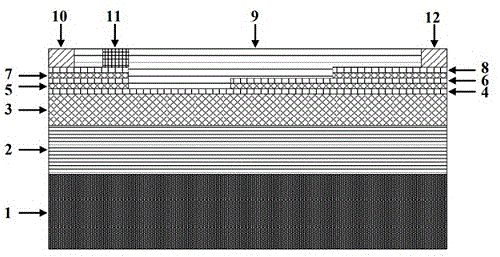
图1显示了本发明一种可变沟道AlGaN/GaN HEMT结构的结构示意图。FIG. 1 shows a schematic structural diagram of a variable channel AlGaN/GaN HEMT structure of the present invention.
图2a-图2e显示了本发明一种可变沟道AlGaN/GaN HEMT结构的制备过程示意图。其中;图2a显示了制备完成的氮化镓多沟道外延片的结构图;图2b显示了刻蚀完成的阶梯槽的结构图;图2c显示了镀设完成的钝化层的结构图;图2d显示了刻蚀完成的电极槽的结构示意图;图2e显示了电极制备完成后的器件结构图。2a-2e show schematic diagrams of the fabrication process of a variable channel AlGaN/GaN HEMT structure of the present invention. Among them; Fig. 2a shows the structure diagram of the prepared gallium nitride multi-channel epitaxial wafer; Fig. 2b shows the structure diagram of the etched stepped groove; Fig. 2c shows the structure diagram of the passivation layer after plating; Figure 2d shows a schematic diagram of the structure of the etched electrode groove; Figure 2e shows the structure of the device after the electrode preparation is completed.
图3显示了本发明的击穿电流电压曲线和一般结构击穿电流电压曲线的比较图。FIG. 3 shows a comparison diagram of the breakdown current-voltage curve of the present invention and the breakdown current-voltage curve of the general structure.
图 4 显示了在同一漏电极电压下,本发明和一般结构在异质结处横向电场分布的比较图。Figure 4 shows a comparison of the lateral electric field distribution at the heterojunction for the inventive and general structures at the same drain voltage.
图 5 显示了在器件击穿时,本发明和一般结构在异质结处横向电场分布的比较图。Figure 5 shows a graph comparing the lateral electric field distribution at the heterojunction for the present invention and the general structure upon device breakdown.
其中有:Including:
1.衬底层;2.缓冲层;1. Substrate layer; 2. Buffer layer;
3.第一组GaN沟道层;4.第一组AlGaN势垒层;3. The first group of GaN channel layers; 4. The first group of AlGaN barrier layers;
5.第二组GaN沟道层;6. 第二组AlGaN势垒层;5. The second group of GaN channel layers; 6. The second group of AlGaN barrier layers;
7.第三组GaN沟道层;8. 第三组AlGaN势垒层;7. The third group of GaN channel layers; 8. The third group of AlGaN barrier layers;
9.钝化层;9. Passivation layer;
91.顶部钝化层;92.阶梯钝化层;93.阶梯槽;931.第一级台阶槽;932. 第二级台阶槽;91. Top passivation layer; 92. Step passivation layer; 93. Step groove; 931. First step groove; 932. Second step groove;
10.源电极;101.源电极槽;10. Source electrode; 101. Source electrode groove;
11.栅电极;111.栅电极槽;11. Gate electrode; 111. Gate electrode groove;
12.漏电极;121.漏电极槽。12. Drain electrode; 121. Drain electrode groove.
具体实施方式Detailed ways
下面结合附图和具体较佳实施方式对本发明作进一步详细的说明。The present invention will be described in further detail below with reference to the accompanying drawings and specific preferred embodiments.
如图1所示,一种可变沟道AlGaN/GaN HEMT结构,包括衬底层1、缓冲层2、n组GaN/AlGaN异质结叠层、钝化层9、源电极10、栅电极11和漏电极12。As shown in FIG. 1, a variable channel AlGaN/GaN HEMT structure includes a
上述衬底层的材质优选为硅、蓝宝石、氮化镓或碳化硅等。The material of the above-mentioned substrate layer is preferably silicon, sapphire, gallium nitride or silicon carbide.
上述缓冲层外延生长在衬底层顶部,优选为厚度2~6微米的GaN材料。The above buffer layer is epitaxially grown on the top of the substrate layer, preferably a GaN material with a thickness of 2-6 microns.
n组GaN/AlGaN异质结叠层从下至上依次外延生长在缓冲层顶部,且从下至上分别为第1组GaN/AlGaN异质结叠层、第2组GaN/AlGaN异质结叠层、……、第n组GaN/AlGaN异质结叠层。其中,n≥2,在本实施例中,优选n=3,也即具有3组GaN/AlGaN异质结叠层。The n groups of GaN/AlGaN heterojunction stacks are epitaxially grown on top of the buffer layer from bottom to top, and from bottom to top are the first group of GaN/AlGaN heterojunction stacks and the second group of GaN/AlGaN heterojunction stacks , ..., the nth group of GaN/AlGaN heterojunction stacks. Wherein, n≧ 2, in this embodiment, preferably n =3, that is, there are three groups of GaN/AlGaN heterojunction stacks.
每组GaN/AlGaN异质结叠层(也称异质结)均包括GaN沟道层和外延生长在GaN沟道层上的AlGaN势垒层。Each set of GaN/AlGaN heterojunction stacks (also called heterojunctions) includes a GaN channel layer and an AlGaN barrier layer epitaxially grown on the GaN channel layer.
上述GaN沟道层优选为厚度0.1~3微米的GaN材料。The above-mentioned GaN channel layer is preferably a GaN material with a thickness of 0.1 to 3 μm.
另外,以摩尔组分计,AlGaN势垒层优选包含0.1~0.3份的Al;AlGaN势垒层的厚度优选为15-30纳米。In addition, in terms of molar composition, the AlGaN barrier layer preferably contains 0.1-0.3 parts of Al; the thickness of the AlGaN barrier layer is preferably 15-30 nm.
上述第1组GaN/AlGaN异质结叠层包括第一组GaN沟道层3和第一组AlGaN势垒层4。The above-mentioned first group of GaN/AlGaN heterojunction stacks includes a first group of GaN channel layers 3 and a first group of AlGaN barrier layers 4 .
上述第2组GaN/AlGaN异质结叠层包括第二组GaN沟道层5和第二组AlGaN势垒层6。The above-mentioned second group of GaN/AlGaN heterojunction stacks includes a second group of GaN channel layers 5 and a second group of AlGaN barrier layers 6 .
上述第3组GaN/AlGaN异质结叠层包括第三组GaN沟道层7和第三组AlGaN势垒层8。The above-mentioned third group of GaN/AlGaN heterojunction stacks includes a third group of GaN channel layers 7 and a third group of AlGaN barrier layers 8 .
钝化层为包括但不限于二氧化硅、氮化硅、氧化铝、二氧化铪等介质材料,钝化层包括顶部钝化层和阶梯钝化层。The passivation layer is a dielectric material including but not limited to silicon dioxide, silicon nitride, aluminum oxide, hafnium dioxide, etc. The passivation layer includes a top passivation layer and a step passivation layer.
顶部钝化层设在第n组GaN/AlGaN异质结叠层顶部。A top passivation layer is provided on top of the nth group of GaN/AlGaN heterojunction stacks.
源电极10和漏电极12,分别嵌设在顶部钝化层x向的两端。The
栅电极11嵌设在邻近源电极的顶部钝化层中部。The
阶梯钝化层嵌设在位于栅电极和漏电极之间的第2组GaN/AlGaN异质结叠层至第n组GaN/AlGaN异质结叠层中;阶梯钝化层呈倒置的阶梯型,且优选厚度深的一端与栅电极相对齐。本发明通过调整阶梯钝化层的阶梯宽度,进而能够调节栅电极和漏电极之间的电荷密度。The stepped passivation layer is embedded in the second group of GaN/AlGaN heterojunction stacks between the gate electrode and the drain electrode to the nth group of GaN/AlGaN heterojunction stacks; the stepped passivation layer is an inverted stepped type , and preferably the end with the deepest thickness is aligned with the gate electrode. The present invention can adjust the charge density between the gate electrode and the drain electrode by adjusting the step width of the step passivation layer.
本发明基于高斯盒分析,以栅电极指向漏电极的方向为x方向,栅电极靠近漏电极的一侧作为原点,缓冲层的厚度为t B,等效浓度为P;阶梯钝化层中半导体层厚度为t S(x),等效浓度为N C,钝化层等效电容为C P,异质结极化电荷等效面密度为σ,电荷量常数为q,GaN材料的临界击穿场强为E C。在理想情况下,GaN材料电场强度达到其临界击穿场强,击穿电压可以达到最高值,则器件结构需满足下式:The invention is based on Gaussian cell analysis, and the direction of the gate electrode pointing to the drain electrode is the x direction, the side of the gate electrode close to the drain electrode is used as the origin, the thickness of the buffer layer is t B , and the equivalent concentration is P ; the semiconductor in the step passivation layer is The layer thickness is t S ( x ), the equivalent concentration is NC , the equivalent capacitance of the passivation layer is C P , the equivalent surface density of the polarized charge of the heterojunction is σ , the charge quantity constant is q , and the critical strike of the GaN material is The penetration field strength is E C . Under ideal conditions, the electric field strength of GaN material reaches its critical breakdown field strength, and the breakdown voltage can reach the highest value, so the device structure needs to satisfy the following formula:
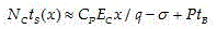
式中,x表示x方向的的刻度或坐标值。In the formula, x represents the scale or coordinate value in the x -direction.
本发明中,阶梯钝化层的设置,使得t S(x)从栅电极向漏电极能够接近线性增加,通过上式可知,能重塑栅电极和漏电极之间的电荷分布,使得栅电极和漏电极之间耗尽区的固定正电荷密度由栅电极向漏电极呈阶梯递增,利用优化后的电荷分布有效调制电场,获得更加均匀的电场分布,从而提高器件的耐压性能。In the present invention, the setting of the step passivation layer enables t S ( x ) to increase linearly from the gate electrode to the drain electrode. It can be seen from the above formula that the charge distribution between the gate electrode and the drain electrode can be reshaped, so that the gate electrode can be reshaped. The fixed positive charge density in the depletion region between the drain electrode and the gate electrode increases in steps from the gate electrode to the drain electrode. The optimized charge distribution is used to effectively modulate the electric field to obtain a more uniform electric field distribution, thereby improving the withstand voltage performance of the device.
如图2a-图2e所示,一种可变沟道AlGaN/GaN HEMT结构的制备方法,包括如下步骤。As shown in Figs. 2a-2e, a method for preparing a variable channel AlGaN/GaN HEMT structure includes the following steps.
步骤1、制备氮化镓多沟道外延片,具体制备方法包括如下步骤。
步骤1A、外延生长缓冲层:清洗衬底层并在衬底层上通过MOCVD外延生长含有GaN材料的缓冲层。Step 1A, epitaxial growth of buffer layer: cleaning the substrate layer and epitaxially growing a buffer layer containing GaN material on the substrate layer by MOCVD.
步骤1B、外延生长第1组GaN/AlGaN异质结叠层:在缓冲层上从下至上依次外延生长GaN沟道层和AlGaN势垒层。Step 1B, epitaxial growth of the first group of GaN/AlGaN heterojunction stacks: epitaxially grow a GaN channel layer and an AlGaN barrier layer on the buffer layer from bottom to top.
步骤1C、外延生长第n组GaN/AlGaN异质结叠层:在第1组GaN/AlGaN异质结叠层上从下至上依次外延生长第2组GaN/AlGaN异质结叠层至第n组GaN/AlGaN异质结叠层,从而形成如图2a所示的氮化镓多沟道外延片。Step 1C, epitaxially growing the nth group of GaN/AlGaN heterojunction stacks: on the first group of GaN/AlGaN heterojunction stacks, epitaxially grow the second group of GaN/AlGaN heterojunction stacks sequentially from bottom to top to the nth group A GaN/AlGaN heterojunction stack is formed to form a gallium nitride multi-channel epitaxial wafer as shown in Figure 2a.
步骤2、刻蚀阶梯槽:在第2组GaN/AlGaN异质结叠层至第n组GaN/AlGaN异质结叠层的中部从上至下依次刻蚀,形成如图2b所示的倒置的阶梯槽93。此时,具有阶梯槽的氮化镓多沟道外延片也称为阶梯多沟道层。
在本实施例中,阶梯槽优选为两级阶梯槽,分别为第一级台阶槽931和第二级台阶槽932;其中,第一级台阶槽竖向贯穿第2组GaN/AlGaN异质结叠层和第3组GaN/AlGaN异质结叠层,也即最大槽深槽;第二级台阶槽竖向贯穿第3组GaN/AlGaN异质结叠层。In this embodiment, the stepped grooves are preferably two-stage stepped grooves, namely the first-stage stepped
步骤3、镀设钝化层:在阶梯槽内部、阶梯槽顶部以及阶梯槽两侧的第n组GaN/AlGaN异质结叠层顶面分别镀介质膜,并进行化学物理抛光,形成如图2c所示的顶面平整的钝化层9;其中,位于阶梯槽内部的钝化层称为阶梯钝化层92,其余钝化层称为顶部钝化层91。Step 3. Plating the passivation layer: the inside of the stepped groove, the top of the stepped groove, and the top surface of the n -th group of GaN/AlGaN heterojunction stacks on both sides of the stepped groove are respectively coated with a dielectric film, and chemically and physically polished to form as shown in the figure. The
本发明中,通过调整阶梯钝化层的阶梯宽度,也即本发明由于拥有非均匀分布的可变多沟道层,可变多沟道层包括多组不同长度的AlGaN/GaN异质结叠层,因而能获得阶梯分布的二维电子气,从而调制器件的电场分布,降低栅电极处的电场峰值,使电场分布均匀化,避免器件的过早击穿,提高器件的耐压性能。In the present invention, by adjusting the step width of the step passivation layer, that is, the present invention has a variable multi-channel layer with a non-uniform distribution, and the variable multi-channel layer includes multiple groups of AlGaN/GaN heterojunction stacks with different lengths. Therefore, a two-dimensional electron gas with a stepped distribution can be obtained, thereby modulating the electric field distribution of the device, reducing the electric field peak value at the gate electrode, making the electric field distribution uniform, avoiding premature breakdown of the device, and improving the withstand voltage performance of the device.
步骤4、刻蚀电极槽
如图2d所示,电极槽包括源电极槽101、漏电极槽121和栅电极槽111。As shown in FIG. 2d , the electrode trench includes a
电极槽的具体刻蚀方法为:在阶梯槽两侧的顶部钝化层两端分别从上至下刻蚀至第n组GaN/AlGaN异质结叠层顶面,形成所述的源电极槽和漏电极槽;其中,源电极槽邻近阶梯槽的最大槽深处(也即邻近第一级台阶槽);在阶梯槽与源电极槽之间的顶部钝化层上从上至下刻蚀至第n组GaN/AlGaN异质结叠层顶面,形成栅电极槽,且栅电极槽的一个侧壁面与阶梯槽的一个侧壁面(优选第一级台阶槽的侧壁面)位于同一竖直平面上。The specific etching method of the electrode groove is as follows: the two ends of the top passivation layer on both sides of the stepped groove are respectively etched from top to bottom to the top surface of the n -th group of GaN/AlGaN heterojunction stacks to form the source electrode groove. and drain electrode groove; wherein, the source electrode groove is adjacent to the maximum groove depth of the stepped groove (that is, adjacent to the first step groove); the top passivation layer between the stepped groove and the source electrode groove is etched from top to bottom To the top surface of the n -th group of GaN/AlGaN heterojunction stacks, a gate electrode trench is formed, and one sidewall surface of the gate electrode trench and one sidewall surface of the stepped trench (preferably the sidewall surface of the first-level stepped trench) are located in the same vertical on flat surface.
步骤5、制备源电极和漏电极:在源电极槽内蒸镀或溅射源电极多元合金,在漏电极槽内蒸镀或溅射漏电极多元合金、并分别退火,则形成源电极和漏电极。Step 5. Preparation of source electrode and drain electrode: Evaporating or sputtering the source electrode multi-element alloy in the source electrode groove, evaporating or sputtering the drain electrode multi-element alloy in the drain electrode groove, and annealing respectively, then the source electrode and the leakage current are formed. pole.
上述退火方式优选为:在850摄氏度和氮气气氛下,退火30秒。The above-mentioned annealing method is preferably: annealing for 30 seconds at 850 degrees Celsius and a nitrogen atmosphere.
步骤6、制备栅电极:在栅电极槽内蒸镀或溅射栅极多元合金,进行金属剥离后,则形成具有肖特基接触的栅电极。
上述源电极、漏电极和栅电极为包括但不限于Ti、Al、Ni、Au等金属的合金。The above-mentioned source electrode, drain electrode and gate electrode are alloys of metals including but not limited to Ti, Al, Ni, Au and the like.
将本发明的器件结构与现有技术中的一般结构进行对比实验,本发明器件能显著提高器件的击穿电压,提升幅度约245%,具体如图3所示。Comparing the device structure of the present invention with the general structure in the prior art, the device of the present invention can significantly improve the breakdown voltage of the device by about 245%, as shown in FIG. 3 .
另外,本发明器件能有效降低栅电极处的电场峰值,拓展耗尽区的宽度,使电场分布更加均匀化,具体如图4所示。In addition, the device of the present invention can effectively reduce the peak value of the electric field at the gate electrode, expand the width of the depletion region, and make the electric field distribution more uniform, as shown in FIG. 4 .
进一步,本发明器件能有效降低栅电极处的电场峰值,拓展耗尽区的宽度,使电场分布更加均匀,避免器件过早击穿,栅电极和漏电极之间的平均电场接近2MV/cm,具体如图5所示。Further, the device of the present invention can effectively reduce the electric field peak value at the gate electrode, expand the width of the depletion region, make the electric field distribution more uniform, avoid premature breakdown of the device, and the average electric field between the gate electrode and the drain electrode is close to 2MV/cm, Specifically as shown in Figure 5.
以上详细描述了本发明的优选实施方式,但是,本发明并不限于上述实施方式中的具体细节,在本发明的技术构思范围内,可以对本发明的技术方案进行多种等同变换,这些等同变换均属于本发明的保护范围。The preferred embodiments of the present invention have been described in detail above. However, the present invention is not limited to the specific details in the above-mentioned embodiments. Within the scope of the technical concept of the present invention, various equivalent transformations can be made to the technical solutions of the present invention. These equivalent transformations All belong to the protection scope of the present invention.
Claims (10)
Priority Applications (1)
| Application Number | Priority Date | Filing Date | Title |
|---|---|---|---|
| CN202210462372.0A CN114582962B (en) | 2022-04-29 | 2022-04-29 | Variable channel AlGaN/GaN HEMT structure and preparation method thereof |
Applications Claiming Priority (1)
| Application Number | Priority Date | Filing Date | Title |
|---|---|---|---|
| CN202210462372.0A CN114582962B (en) | 2022-04-29 | 2022-04-29 | Variable channel AlGaN/GaN HEMT structure and preparation method thereof |
Publications (2)
| Publication Number | Publication Date |
|---|---|
| CN114582962A CN114582962A (en) | 2022-06-03 |
| CN114582962B true CN114582962B (en) | 2022-07-22 |
Family
ID=81784624
Family Applications (1)
| Application Number | Title | Priority Date | Filing Date |
|---|---|---|---|
| CN202210462372.0A Active CN114582962B (en) | 2022-04-29 | 2022-04-29 | Variable channel AlGaN/GaN HEMT structure and preparation method thereof |
Country Status (1)
| Country | Link |
|---|---|
| CN (1) | CN114582962B (en) |
Families Citing this family (1)
| Publication number | Priority date | Publication date | Assignee | Title |
|---|---|---|---|---|
| WO2024254229A1 (en) * | 2023-06-07 | 2024-12-12 | Efficient Power Conversion Corporation | GaN TRANSISTOR HAVING MULTI-THICKNESS FRONT BARRIER |
Family Cites Families (4)
| Publication number | Priority date | Publication date | Assignee | Title |
|---|---|---|---|---|
| CN102130158B (en) * | 2011-01-05 | 2012-07-25 | 西安电子科技大学 | Step-like groove-grid high electron mobility transistor |
| CN103489897B (en) * | 2013-08-21 | 2017-04-26 | 中国电子科技集团公司第十三研究所 | Quasi-linear doped device structure based on group III nitride material |
| CN109285884A (en) * | 2017-07-19 | 2019-01-29 | 吴绍飞 | Stepped Recessed Gate High Electron Mobility Transistor |
| CN114141871A (en) * | 2021-11-29 | 2022-03-04 | 迪优未来科技(清远)有限公司 | A kind of high withstand voltage enhanced HEMT device and preparation method thereof |
-
2022
- 2022-04-29 CN CN202210462372.0A patent/CN114582962B/en active Active
Also Published As
| Publication number | Publication date |
|---|---|
| CN114582962A (en) | 2022-06-03 |
Similar Documents
| Publication | Publication Date | Title |
|---|---|---|
| US12284818B2 (en) | High-threshold-voltage normally-off high-electron-mobility transistor and preparation method therefor | |
| US10103219B2 (en) | Power semiconductor device and method for manufacturing the same | |
| US11276765B2 (en) | Composite-channel high electron mobility transistor | |
| CN111682064B (en) | High-performance MIS gate enhancement mode GaN-based high electron mobility transistor and preparation method thereof | |
| CN111863948B (en) | A GaN-based P-GaN enhanced HEMT device with a gate-source bridge and a method for preparing the same | |
| CN109873034B (en) | Normally-off HEMT power device for depositing polycrystalline AlN and preparation method thereof | |
| WO2006001369A1 (en) | Semiconductor device | |
| CN102130159A (en) | High Electron Mobility Transistor | |
| WO2021139041A1 (en) | Gallium oxide schottky diode and preparation method therefor | |
| CN109037327A (en) | A kind of longitudinal gate structure power device and preparation method thereof with local current barrier layer | |
| US12034067B2 (en) | GaN-HEMT device with sandwich structure and method for preparing the same | |
| CN100433365C (en) | Aluminium gallium nitride/gallium nitride high electronic migration rate transistor and its manufacturing method | |
| CN114582962B (en) | Variable channel AlGaN/GaN HEMT structure and preparation method thereof | |
| CN209447804U (en) | A kind of semiconductor structure | |
| CN119403168B (en) | GaN high electron mobility transistor structure based on double grid electrodes and preparation method | |
| CN117438457B (en) | Recessed gate GaN-based HEMT device and preparation method thereof | |
| CN209447805U (en) | A kind of semiconductor structure | |
| CN111785783A (en) | A two-dimensional AlN/GaN HEMT radio frequency device and preparation method thereof | |
| CN111415998A (en) | GaN-based Schottky diode and preparation method thereof | |
| CN108831932B (en) | A GaN Lateral MIS-Schottky Hybrid Anode Diode | |
| CN117276354A (en) | A hybrid anode Schottky diode and its preparation method and application | |
| CN209515674U (en) | GaN-HEMT device with sandwich structure | |
| CN209766426U (en) | A normally-off HEMT device with deposited polycrystalline AlN | |
| CN209447803U (en) | A kind of semiconductor structure | |
| CN115241292A (en) | A vertical gallium nitride-based fin-type radio frequency transistor and preparation method thereof |
Legal Events
| Date | Code | Title | Description |
|---|---|---|---|
| PB01 | Publication | ||
| PB01 | Publication | ||
| SE01 | Entry into force of request for substantive examination | ||
| SE01 | Entry into force of request for substantive examination | ||
| GR01 | Patent grant | ||
| GR01 | Patent grant |