CN114374082A - Radiating element and base station antenna - Google Patents
Radiating element and base station antenna Download PDFInfo
- Publication number
- CN114374082A CN114374082A CN202011100811.0A CN202011100811A CN114374082A CN 114374082 A CN114374082 A CN 114374082A CN 202011100811 A CN202011100811 A CN 202011100811A CN 114374082 A CN114374082 A CN 114374082A
- Authority
- CN
- China
- Prior art keywords
- conductive
- loop
- radiating element
- section
- dipole arm
- Prior art date
- Legal status (The legal status is an assumption and is not a legal conclusion. Google has not performed a legal analysis and makes no representation as to the accuracy of the status listed.)
- Pending
Links
- 230000001747 exhibiting effect Effects 0.000 claims abstract 2
- 230000008878 coupling Effects 0.000 claims description 35
- 238000010168 coupling process Methods 0.000 claims description 35
- 238000005859 coupling reaction Methods 0.000 claims description 35
- 239000002184 metal Substances 0.000 claims description 12
- 239000000758 substrate Substances 0.000 claims description 12
- 238000003491 array Methods 0.000 description 22
- 230000005855 radiation Effects 0.000 description 7
- 230000000694 effects Effects 0.000 description 5
- 230000010267 cellular communication Effects 0.000 description 3
- 230000001413 cellular effect Effects 0.000 description 3
- 238000004891 communication Methods 0.000 description 2
- 238000012986 modification Methods 0.000 description 2
- 230000004048 modification Effects 0.000 description 2
- 238000010276 construction Methods 0.000 description 1
- 230000007812 deficiency Effects 0.000 description 1
- 238000010586 diagram Methods 0.000 description 1
- 238000001914 filtration Methods 0.000 description 1
- 238000000034 method Methods 0.000 description 1
- 238000004904 shortening Methods 0.000 description 1
- 230000008054 signal transmission Effects 0.000 description 1
- 230000003746 surface roughness Effects 0.000 description 1
- 238000013316 zoning Methods 0.000 description 1
Images


Classifications
-
- H—ELECTRICITY
- H01—ELECTRIC ELEMENTS
- H01Q—ANTENNAS, i.e. RADIO AERIALS
- H01Q1/00—Details of, or arrangements associated with, antennas
- H01Q1/36—Structural form of radiating elements, e.g. cone, spiral, umbrella; Particular materials used therewith
-
- H—ELECTRICITY
- H01—ELECTRIC ELEMENTS
- H01Q—ANTENNAS, i.e. RADIO AERIALS
- H01Q1/00—Details of, or arrangements associated with, antennas
- H01Q1/12—Supports; Mounting means
- H01Q1/22—Supports; Mounting means by structural association with other equipment or articles
- H01Q1/24—Supports; Mounting means by structural association with other equipment or articles with receiving set
- H01Q1/241—Supports; Mounting means by structural association with other equipment or articles with receiving set used in mobile communications, e.g. GSM
- H01Q1/246—Supports; Mounting means by structural association with other equipment or articles with receiving set used in mobile communications, e.g. GSM specially adapted for base stations
-
- H—ELECTRICITY
- H01—ELECTRIC ELEMENTS
- H01Q—ANTENNAS, i.e. RADIO AERIALS
- H01Q1/00—Details of, or arrangements associated with, antennas
- H01Q1/36—Structural form of radiating elements, e.g. cone, spiral, umbrella; Particular materials used therewith
- H01Q1/38—Structural form of radiating elements, e.g. cone, spiral, umbrella; Particular materials used therewith formed by a conductive layer on an insulating support
-
- H—ELECTRICITY
- H01—ELECTRIC ELEMENTS
- H01Q—ANTENNAS, i.e. RADIO AERIALS
- H01Q1/00—Details of, or arrangements associated with, antennas
- H01Q1/52—Means for reducing coupling between antennas; Means for reducing coupling between an antenna and another structure
- H01Q1/521—Means for reducing coupling between antennas; Means for reducing coupling between an antenna and another structure reducing the coupling between adjacent antennas
-
- H—ELECTRICITY
- H01—ELECTRIC ELEMENTS
- H01Q—ANTENNAS, i.e. RADIO AERIALS
- H01Q21/00—Antenna arrays or systems
- H01Q21/06—Arrays of individually energised antenna units similarly polarised and spaced apart
- H01Q21/061—Two dimensional planar arrays
- H01Q21/062—Two dimensional planar arrays using dipole aerials
-
- H—ELECTRICITY
- H01—ELECTRIC ELEMENTS
- H01Q—ANTENNAS, i.e. RADIO AERIALS
- H01Q21/00—Antenna arrays or systems
- H01Q21/24—Combinations of antenna units polarised in different directions for transmitting or receiving circularly and elliptically polarised waves or waves linearly polarised in any direction
- H01Q21/26—Turnstile or like antennas comprising arrangements of three or more elongated elements disposed radially and symmetrically in a horizontal plane about a common centre
-
- H—ELECTRICITY
- H01—ELECTRIC ELEMENTS
- H01Q—ANTENNAS, i.e. RADIO AERIALS
- H01Q25/00—Antennas or antenna systems providing at least two radiating patterns
- H01Q25/001—Crossed polarisation dual antennas
-
- H—ELECTRICITY
- H01—ELECTRIC ELEMENTS
- H01Q—ANTENNAS, i.e. RADIO AERIALS
- H01Q5/00—Arrangements for simultaneous operation of antennas on two or more different wavebands, e.g. dual-band or multi-band arrangements
- H01Q5/30—Arrangements for providing operation on different wavebands
- H01Q5/307—Individual or coupled radiating elements, each element being fed in an unspecified way
- H01Q5/314—Individual or coupled radiating elements, each element being fed in an unspecified way using frequency dependent circuits or components, e.g. trap circuits or capacitors
- H01Q5/321—Individual or coupled radiating elements, each element being fed in an unspecified way using frequency dependent circuits or components, e.g. trap circuits or capacitors within a radiating element or between connected radiating elements
-
- H—ELECTRICITY
- H01—ELECTRIC ELEMENTS
- H01Q—ANTENNAS, i.e. RADIO AERIALS
- H01Q5/00—Arrangements for simultaneous operation of antennas on two or more different wavebands, e.g. dual-band or multi-band arrangements
- H01Q5/30—Arrangements for providing operation on different wavebands
- H01Q5/307—Individual or coupled radiating elements, each element being fed in an unspecified way
- H01Q5/342—Individual or coupled radiating elements, each element being fed in an unspecified way for different propagation modes
- H01Q5/357—Individual or coupled radiating elements, each element being fed in an unspecified way for different propagation modes using a single feed point
- H01Q5/364—Creating multiple current paths
-
- H—ELECTRICITY
- H01—ELECTRIC ELEMENTS
- H01Q—ANTENNAS, i.e. RADIO AERIALS
- H01Q5/00—Arrangements for simultaneous operation of antennas on two or more different wavebands, e.g. dual-band or multi-band arrangements
- H01Q5/40—Imbricated or interleaved structures; Combined or electromagnetically coupled arrangements, e.g. comprising two or more non-connected fed radiating elements
- H01Q5/48—Combinations of two or more dipole type antennas
-
- H—ELECTRICITY
- H01—ELECTRIC ELEMENTS
- H01Q—ANTENNAS, i.e. RADIO AERIALS
- H01Q9/00—Electrically-short antennas having dimensions not more than twice the operating wavelength and consisting of conductive active radiating elements
- H01Q9/04—Resonant antennas
- H01Q9/16—Resonant antennas with feed intermediate between the extremities of the antenna, e.g. centre-fed dipole
- H01Q9/28—Conical, cylindrical, cage, strip, gauze, or like elements having an extended radiating surface; Elements comprising two conical surfaces having collinear axes and adjacent apices and fed by two-conductor transmission lines
- H01Q9/285—Planar dipole
Landscapes
- Engineering & Computer Science (AREA)
- Computer Networks & Wireless Communication (AREA)
- Physics & Mathematics (AREA)
- Electromagnetism (AREA)
- Variable-Direction Aerials And Aerial Arrays (AREA)
- Details Of Aerials (AREA)
Abstract
Description
技术领域technical field
本公开一般涉及无线电通信,更具体地说,涉及一种用于蜂窝通信系统的辐射元件以及基站天线。The present disclosure relates generally to radio communications, and more particularly, to a radiating element and base station antenna for a cellular communication system.
背景技术Background technique
蜂窝通信系统在本领域中是公知的。在蜂窝通信系统中,地理区域被分成一系列区域,这些区域被称为由各个基站服务的“小区”。基站可以包括一个或多个基站天线,其被配置为提供与由基站服务的小区内的移动订户的双向射频(“RF”)通信。Cellular communication systems are well known in the art. In a cellular communication system, a geographic area is divided into a series of areas called "cells" served by various base stations. A base station may include one or more base station antennas configured to provide two-way radio frequency ("RF") communication with mobile subscribers within a cell served by the base station.
在许多情况下,每个基站被划分为各“扇区”。在最常见的配置中,六角形小区分为三个120°扇区,每个扇区由一个或多个基站天线提供服务,其方位半功率波束宽度(HPBW)约为65°。通常,基站天线安装在塔架结构上,其中由基站天线产生的辐射图案(这里也称为“天线波束”)向外指向。基站天线通常实现为辐射元件的线性或平面相控阵列。In many cases, each base station is divided into "sectors". In the most common configuration, a hexagonal cell is divided into three 120° sectors, each served by one or more base station antennas, with an azimuth half-power beamwidth (HPBW) of approximately 65°. Typically, base station antennas are mounted on a tower structure with the radiation patterns (also referred to herein as "antenna beams") produced by the base station antennas directed outward. Base station antennas are typically implemented as linear or planar phased arrays of radiating elements.
为了适应日益增长的蜂窝通信量,蜂窝运营商已经在各种新的频带中增加了蜂窝服务。虽然在一些情况下,有可能使用所谓的“宽带”或“超宽带”辐射元件的线性阵列来在多个频带中提供服务,但在其它情况下,需要使用不同的辐射元件的线性阵列或平面阵列来支持不同频带中的服务。To accommodate increasing cellular traffic, cellular operators have added cellular service in various new frequency bands. While in some cases it is possible to use linear arrays of so-called "broadband" or "ultra-broadband" radiating elements to provide service in multiple frequency bands, in other cases it is necessary to use linear arrays or planes of different radiating elements arrays to support services in different frequency bands.
随着频带数量的增加,扇区化的增加变得越来越普遍(例如,将小区划分成六个、九个或者甚至十二个扇区),并且在典型的基站处部署的基站天线的数量显著增加。然而,由于本地分区条例和/或天线塔的重量以及风力载荷限制等原因,对于可以在给定基站处部署的基站天线的数量经常存在限制。为了在不进一步增加基站天线数量的情况下增加容量,已经引入了所谓的多频带基站天线,其中辐射元件的多个线性阵列被包括在单个天线中。一种非常常见的多频带基站天线包括用于在617-960MHz频带中的一些或全部中提供服务的“低频带”辐射元件的一个线性阵列;用于在1427-2690MHz频带中的一些或全部中提供服务的“中频带”辐射元件的两个或四个线性阵列。这些辐射元件的线性阵列典型地以并排方式安装。Increased sectorization (eg, dividing a cell into six, nine, or even twelve sectors) becomes more common as the number of frequency bands increases, and the number of base station antennas deployed at a typical base station is The number has increased significantly. However, there are often limitations on the number of base station antennas that can be deployed at a given base station due to local zoning regulations and/or antenna tower weight and wind load limitations, among other reasons. In order to increase capacity without further increasing the number of base station antennas, so-called multi-band base station antennas have been introduced, in which multiple linear arrays of radiating elements are included in a single antenna. A very common multi-band base station antenna includes a linear array of "low-band" radiating elements for serving in some or all of the 617-960MHz band; for use in some or all of the 1427-2690MHz band Two or four linear arrays of serving "mid-band" radiating elements. Linear arrays of these radiating elements are typically mounted side by side.
然而,随着辐射元件的线性阵列更接近地排列在一起,线性阵列之间信号耦合度可能增加。例如,低频带辐射元件之间或高频带辐射元件之间的耦合干扰可能增加。此外,低频带辐射元件会对附近区域的中频带辐射元件产生较大散射影响(scatteringeffect)。这种耦合干扰可能负面地影响相应中频带线性阵列的辐射方向图的特性。然而,低频带辐射元件的任何尺寸变化也通常会影响低频带辐射元件的射频性能、例如改变自身的工作频带、HPBW的增加等。However, as linear arrays of radiating elements are arranged closer together, the degree of signal coupling between linear arrays may increase. For example, coupling interference between low-band radiating elements or between high-band radiating elements may increase. In addition, the low-band radiating elements can have a larger scattering effect on the mid-band radiating elements in the vicinity. Such coupling disturbances may negatively affect the characteristics of the radiation pattern of the corresponding mid-band linear array. However, any dimensional change of the low-band radiating element will also generally affect the radio frequency performance of the low-band radiating element, such as changing its own operating frequency band, increasing the HPBW, etc.
公开内容public content
因此,本公开的目的在于提供一种能够克服现有技术中至少一个缺陷的辐射元件以及相关的基站天线。Therefore, it is an object of the present disclosure to provide a radiating element and related base station antenna that can overcome at least one of the deficiencies in the prior art.
按照本公开的第一方面,提供一种辐射元件,所述辐射元件的偶极臂可以包括第一导电线路环和与第一导电线路环至少部分分离的第二导电线路环。所述第一导电线路环可以包括至少一个窄导电区段和至少一个宽导电区段。所述窄导电区段可以在该辐射元件的工作频带之外的至少一个频带内呈现高阻抗特性,以便至少部分地抑制在所述至少一个频带内的电流。According to a first aspect of the present disclosure, there is provided a radiating element, the dipole arm of which may include a first loop of conductive traces and a second loop of conductive traces at least partially separated from the first loop of conductive traces. The first conductive trace loop may include at least one narrow conductive segment and at least one wide conductive segment. The narrow conductive section may exhibit high impedance characteristics in at least one frequency band outside the operating frequency band of the radiating element so as to at least partially suppress current flow in the at least one frequency band.
按照本公开的第二方面,提供一种辐射元件,所述辐射元件的偶极臂可以包括第一导电线路环和第二导电线路环。所述第一导电线路环可以设置在介质基板的第一主表面上,第二导电线路环的第一部分可以设置在介质基板的第一主表面上,而第二导电线路环的第二部分可以设置在介质基板的第二主表面上。According to a second aspect of the present disclosure, there is provided a radiating element, a dipole arm of which may include a first loop of conductive traces and a second loop of conductive traces. The first loop of conductive traces may be disposed on the first major surface of the dielectric substrate, the first portion of the second loop of conductive traces may be disposed on the first major surface of the dielectric substrate, and the second portion of the second loop of conductive traces may be disposed on the first major surface of the dielectric substrate disposed on the second main surface of the dielectric substrate.
按照本公开的第三方面,提供一种基站天线,所述基站天线包括馈电板以及安装在馈电板上的根据本公开所述的辐射元件。According to a third aspect of the present disclosure, there is provided a base station antenna including a feeder plate and a radiating element according to the present disclosure mounted on the feeder plate.
附图说明Description of drawings
图中:In the picture:
图1示出根据本公开一些实施例的基站天线的示意性立体图;1 shows a schematic perspective view of a base station antenna according to some embodiments of the present disclosure;
图2示出图1的基站天线中的天线组件的示意性正视图;Figure 2 shows a schematic front view of an antenna assembly in the base station antenna of Figure 1;
图3示出根据本公开的一些实施例的辐射元件的示意性立体图;Figure 3 shows a schematic perspective view of a radiating element according to some embodiments of the present disclosure;
图4示出图3的辐射元件的示意性电流分布图;Fig. 4 shows a schematic current distribution diagram of the radiating element of Fig. 3;
图5a示出根据本公开的一些实施例的辐射元件的示意性正视图,附加地示出了在介质板的第二主表面上的附加导电区段;Figure 5a shows a schematic front view of a radiating element according to some embodiments of the present disclosure, additionally showing additional conductive segments on the second major surface of the dielectric plate;
图5b示出图5a的辐射元件的设置在介质板的第一主表面上的偶极臂部分的示意图;Figure 5b shows a schematic view of the dipole arm portion of the radiating element of Figure 5a disposed on the first major surface of the dielectric plate;
图5c示出图5a的辐射元件的设置在介质板的第二主表面上的偶极臂部分的示意图。Figure 5c shows a schematic view of the dipole arm portion of the radiating element of Figure 5a disposed on the second major surface of the dielectric plate.
具体实施方式Detailed ways
以下将参照附图描述本公开,其中的附图示出了本公开的若干实施例。然而应当理解的是,本公开可以以多种不同的方式呈现出来,并不局限于下文描述的实施例;事实上,下文描述的实施例旨在使本公开的公开更为完整,并向本领域技术人员充分说明本公开的保护范围。还应当理解的是,本文公开的实施例能够以各种方式进行组合,从而提供更多额外的实施例。The present disclosure will be described below with reference to the accompanying drawings, which illustrate several embodiments of the disclosure. It should be understood, however, that this disclosure may be presented in many different forms and is not limited to the embodiments described below; Those skilled in the art will fully explain the protection scope of the present disclosure. It should also be understood that the embodiments disclosed herein can be combined in various ways to provide still further embodiments.
应当理解的是,在所有附图中,相同的附图标记表示相同的元件。在附图中,为清楚起见,某些特征的尺寸可以进行变形。It should be understood that the same reference numerals refer to the same elements throughout the drawings. In the drawings, the dimensions of certain features may be varied for clarity.
应当理解的是,说明书中的用辞仅用于描述特定的实施例,并不旨在限定本公开。说明书使用的所有术语(包括技术术语和科学术语)除非另外定义,均具有本领域技术人员通常理解的含义。为简明和/或清楚起见,公知的功能或结构可以不再详细说明。It should be understood that the phraseology in the specification is used to describe particular embodiments only and is not intended to limit the present disclosure. All terms (including technical and scientific terms) used in the specification have the meanings commonly understood by those skilled in the art unless otherwise defined. Well-known functions or constructions may not be described in detail for brevity and/or clarity.
说明书使用的单数形式“一”、“所述”和“该”除非清楚指明,均包含复数形式。说明书使用的用辞“包括”、“包含”和“含有”表示存在所声称的特征,但并不排斥存在一个或多个其它特征。说明书使用的用辞“和/或”包括相关列出项中的一个或多个的任意和全部组合。说明书使用的用辞“在X和Y之间”和“在大约X和Y之间”应当解释为包括X和Y。本说明书使用的用辞“在大约X和Y之间”的意思是“在大约X和大约Y之间”,并且本说明书使用的用辞“从大约X至Y”的意思是“从大约X至大约Y”。As used in this specification, the singular forms "a", "the" and "the" include the plural forms unless clearly indicated otherwise. The terms "comprising", "including" and "containing" are used in the specification to indicate the presence of a claimed feature, but not to exclude the presence of one or more other features. As used in this specification, the term "and/or" includes any and all combinations of one or more of the associated listed items. The terms "between X and Y" and "between about X and Y" used in the specification should be construed to include both X and Y. As used in this specification, the phrase "between about X and Y" means "between about X and about Y," and as used in this specification, the phrase "from about X to Y" means "from about X to Y" to about Y".
在说明书中,称一个元件位于另一元件“上”、“附接”至另一元件、“连接”至另一元件、“耦合”至另一元件、或“接触”另一元件等时,该元件可以直接位于另一元件上、附接至另一元件、连接至另一元件、联接至另一元件或接触另一元件,或者可以存在中间元件。相对照的是,称一个元件“直接”位于另一元件“上”、“直接附接”至另一元件、“直接连接”至另一元件、“直接耦合”至另一元件或、或“直接接触”另一元件时,将不存在中间元件。在说明书中,一个特征布置成与另一特征“相邻”,可以指一个特征具有与相邻特征重叠的部分或者位于相邻特征上方或下方的部分。In the specification, when an element is referred to as being "on", "attached" to, "connected" to, "coupled" to, or "contacting" another element, etc. The element may be directly on, attached to, connected to, coupled to, or in contact with another element, or intervening elements may be present. In contrast, an element is referred to as being "directly on" another element, "directly attached" to another element, "directly connected" to another element, "directly coupled" to another element or, or "directly coupled" to another element. When directly contacting" another element, there will be no intervening elements. In the specification, a feature is arranged "adjacent" to another feature, which can mean that one feature has a portion that overlaps an adjacent feature or a portion that is above or below an adjacent feature.
在说明书中,诸如“上”、“下”、“左”、“右”、“前”、“后”、“高”、“低”等的空间关系用辞可以说明一个特征与另一特征在附图中的关系。应当理解的是,空间关系用辞除了包含附图所示的方位之外,还包含装置在使用或操作中的不同方位。例如,在附图中的装置倒转时,原先描述为在其它特征“下方”的特征,此时可以描述为在其它特征的“上方”。装置还可以以其它方式定向(旋转90度或在其它方位),此时将相应地解释相对空间关系。In the specification, spatially relative terms such as "up," "down," "left," "right," "front," "rear," "high," "low," etc. may describe one feature versus another relationship in the attached drawing. It should be understood that spatially relative terms encompass different orientations of the device in use or operation in addition to the orientation shown in the figures. For example, when the device in the figures is turned over, features previously described as "below" other features may now be described as "above" the other features. The device may also be otherwise oriented (rotated 90 degrees or at other orientations) in which case the relative spatial relationships will be interpreted accordingly.
现在将参考附图更详细地描述本公开的一些实施例。Some embodiments of the present disclosure will now be described in more detail with reference to the accompanying drawings.
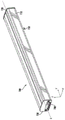
图1示出根据本公开一些实施例的基站天线100的示意性立体图;图2示出在图1的基站天线100中的天线组件200的示意性正视图。FIG. 1 shows a schematic perspective view of a
如图1所示,基站天线100是沿纵轴线L延伸的细长结构。基站天线100可以具有大致矩形横截面的管状形状。基站天线100包括天线罩110和顶端盖120。一个或多个安装支架150设置在天线罩110的后侧,其可用于将基站天线100安装到例如天线塔上的天线支架150(未示出)上。基站天线100还包括底端盖130,底端盖130包括安装在其中的多个连接器140。基站天线100通常以竖直方式安装(即,当基站天线100处于正常运行中时,纵轴线L可大致垂直于由地平线限定的平面)。As shown in FIG. 1, the
如图2所示,基站天线100包括可滑动地插入天线罩110的天线组件200。天线组件200包括反射体210以及安装在反射体210上的多个辐射元件阵列。反射体210可以用作各辐射元件的接地平面结构,并且各辐射元件被安装成从反射体210向前(沿着前向方向F)延伸。这些阵列例如可以是线性辐射元件阵列或者二维辐射元件阵列。在一些实施例中,各阵列可以基本上沿着基站天线100的整个长度延伸。在其他实施例中,各阵列也可以仅局部地沿着基站天线100的长度尺寸延伸。这些阵列可以沿竖直方向V从基站天线100的下端部延伸到上端部,竖直方向V可以是基站天线100的纵轴线L的方向或者与纵轴线L平行。该竖直方向V垂直于水平方向H和前向方向F(见图1)。As shown in FIG. 2 , the
在图2的实施例中,示例性地示出了六个辐射元件线性阵列:两个低频带阵列302-1、302-2、两个中频带阵列402-1、402-2和两个中频带阵列502-1、502-2,其中,仅示意性地每个阵列具有一个低频带辐射元件300来代表两个低频带阵列302-1,302-2。低频带辐射元件300的工作频带例如可以为617MHz至960MHz或者其中的一个或多个部分范围。中频带辐射元件400的工作频带例如可以为1427MHz至2690MHz或者其中的一个或多个部分范围。中频带辐射元件500的工作频带可以是1690至2690MHz或者其中的一个或多个部分范围。在其他实施例中,也可以提供高频带辐射元件阵列,其工作频带可以是3GHz至5.8GHz或者其中的一个或多个部分范围。In the embodiment of Figure 2, six linear arrays of radiating elements are exemplarily shown: two low-band arrays 302-1, 302-2, two mid-band arrays 402-1, 402-2, and two mid-band arrays The frequency band arrays 502-1, 502-2, wherein each array has only one low frequency
接下去,将参考附图3和4更详细地描述根据本公开的一些实施例的辐射元件300。在图3和4的实施例中,辐射元件300可以构成为图2中的低频带辐射元件,其可以被配置为在例如617-960MHz频率范围或其一部分的频带中发送和接收RF信号。在其他实施例中,辐射元件也可以构成为其他频带辐射元件。在其他实施例中,辐射元件300还可以构成为宽频带辐射元件。Next, the radiating
图3示出辐射元件300的示意性立体图。在图3的实施例中,辐射元件300包括由钣金件形成的交叉辐射器。所述交叉辐射器可以支承在作为支承结构360的介质板上。钣金件辐射器是有利的:第一,钣金件辐射器的成本便宜;第二,钣金件辐射器可以具有任何期望的厚度,并且可以表现出改善的阻抗匹配和/或降低的信号传输损耗;第三,钣金件辐射器可以容易地获得具有较低水平的表面粗糙度,并且可以表现出改善的无源互调(“PIM”)失真性能。FIG. 3 shows a schematic perspective view of a
交叉辐射器结构包括第一偶极辐射器和第二偶极辐射器。每个偶极辐射器包括一对偶极臂310。应理解的是,在本公开中并不限制偶极臂310的具体构成方式。在其他实施例中,辐射元件的偶极臂310也可以构成为包括印制的金属图案的印刷电路板偶极臂。The crossed radiator structure includes a first dipole radiator and a second dipole radiator. Each dipole radiator includes a pair of
辐射元件300的每个偶极臂310可以分别包括由至少一个窄导电区段370和至少一个宽导电区段380构成的环状臂或者说导电线路环(以下称为第一导电线路环330)。每个第一导电线路环330可以包括两条导电路径,第一导电路径形成偶极臂310的一半,第二导电路径形成该偶极臂310的另一半。窄导电区段370可以构成为弯曲的臂区段以增加其路径长度,从而有利于辐射元件300的紧凑度和/或相对于高频带辐射的所需滤波效果。宽导电区段380可具有第一宽度,窄导电区段370可以具有第二宽度。各宽导电区段380的第一宽度和各窄导电区段370的第二宽度不必相同。因此,在某些情况下,参考宽导电区段380和窄导电区段370的平均宽度。各宽导电区段380的平均宽度可以是例如至少各窄导电区段370的平均宽度的两倍。在其他情况下,各宽导电区段380的平均宽度可以是例如至少各窄导电区段370的平均宽度的三倍、四倍、五倍、六倍、八倍或十倍。Each
第一导电路径和第二导电路径至少在部分区段上彼此间隔开距离,也就是说,在第一导电路径和第二导电路径之间存在间隙320。在一些情况下,第一导电路径的第一宽导电区段380和与之相对置的第二导电路径的第二宽导电区段380之间的间隙320可以是宽导电区段380第一宽度的2.5、2、1.75、1.5、1.25、1或0.5倍。较大的间隙有利于缩短偶极臂310的端至端长度并且因此有助于辐射元件300的紧凑度。The first conductive path and the second conductive path are spaced apart from each other at least over a partial section, that is, a
此外,弯曲的窄导电区段370可以被实现为非线性导电区段,其可以作为高阻抗部分至少部分地抑制或者说中断否则可能在第一导电线路环330上感应出的高频带和/或中频带范围内的电流。这样,窄导电区段370可以减少在低频带辐射元件300上感应出的高频带和/或中频带电流,从而进一步减小低频带辐射元件300对高频带和/或中频带辐射元件的散射影响。窄导电区段370可以使第一导电线路环330几乎对高频带和/或中频带辐射元件不可见,因此使低频带辐射元件300具有隐身功能。具有隐身功能的低频带辐射元件300是有利的,在低频带辐射元件300的偶极臂310上感应出高频带和/或中频带电流的程度越小,对高频带和/或中频带辐射元件的线性阵列的辐射方向图特性的影响就越小。Furthermore, the curved narrow
然而,由于辐射元件300的偶极臂310的第一导电线路环330的设计方案,辐射元件300的与第一导电线路环330有关的工作频带会发生变化。例如,工作频带可能变窄和/或工作频带的中心频率的位置可能会偏移。工作频带的这些变化负面地影响辐射元件300在其设定的工作频带内稳定的RF性能。在一些实施例中,辐射元件300的设定工作频带例如可以为617-960MHz。但是,辐射元件300的第一导电线路环330无法在整个工作频带内工作。例如,在一些实施例中,第一导电线路环330仅能在子频带617-860MHz上工作,而在子频带860-960MHz上无法获得良好的辐射性能。在其他实施例中,第一导电线路环330仅能符合要求地在子频带760-960MHz上工作,而在子频带617-760MHz上无法获得良好的辐射性能。However, due to the design of the first
为了改善辐射元件300在预定的工作频带内的RF性能,提出一种基于多谐振电路的偶极臂310。继续参照图3,所述辐射元件300的偶极臂310可以包括多个导电线路环。在图3实施例中,偶极臂310可以包括第一导电线路环330和第二导电线路环340。第一导电线路环330可以被构造成第一谐振电路,其可以针对辐射元件300的工作频带内的第一子频带设计而成。第二导电线路环340可以被构造成第二谐振电路,其可以针对辐射元件300的工作频带内的第二子频带设计而成。换句话说,第一谐振电路的谐振频点可以设计成第一子频带的中心频率,而第二谐振电路的谐振频点可以设计成第二子频带的中心频率。第一谐振电路的谐振频点小于第二谐振电路的谐振频点。第一子频带和第二子频带可以分别占据工作频带的一部分并且共同构成整个工作频带。在图3的实施例中,第一子频带和第二子频带可以设计成具有部分重叠的频带或者具有完全分离的频带。在一些实施例中,第一子频带可以设计为工作频带的较低部分,例如617-860MHz,而第二子频带可以设计为工作频带的较高部分,例如860-960MHz。在其他实施例中,第一子频带可以设计为工作频带的较低部分,例如617-900MHz,而第二子频带可以设计为工作频带的较低部分,例如860-960MHz。在其他实施例中,第一子频带可以设计为工作频带的较高部分,而第二子频带可以设计为工作频带的较低部分。In order to improve the RF performance of the radiating
在图3的实施例中,第二导电线路环340可以处于第一导电线路环330内并且与第一导电线路环330具有共同导电区段。所述共同导电区段可以包括第一导电线路环330上的至少一部分宽导电区段和/或至少一部分窄导电区段。此外,辐射元件的偶极臂还可以包括附加导电区段350,所述附加导电区段350可以作为单独附属于第二导电线路环340的分离区段跨接在第一导电线路环330内。附加导电区段350可以被构造成短接第一导电线路环330。在一些实施例中,附加导电区段350可以从第一导电线路环330的第一宽导电区段跨接至第二宽导电区段、例如对置的第二宽导电区段,由此与共同导电区段一同电连接成第二导电线路环340。在其他实施例中,附加导电区段350也可以从第一导电线路环330的任一宽导电区段跨接至任一窄导电区段,或者从第一导电线路环330的任一窄导电区段跨接至任一宽或窄导电区段。为了设置所述附加导电区段350,辐射元件的支承结构360可以相应地设有跨接第一导电线路环330的跨接部361。附加导电区段350可以具有较窄的尺寸、例如可以具有小于等于2mm、1.5mm、1mm、0.8mm、0.7mm、0.5mm、0.2mm的宽度。在一些实施例中,附加导电区段350也可以构成为弯曲的非线性导电区段。附加导电区段350可以作为高阻抗部分至少部分地抑制或中断否则可能在第二导电线路环340上感应出的高频带和/或中频带范围内的电流,从而进一步减小低频带辐射元件300对高频带和/或中频带辐射元件的散射影响。In the embodiment of FIG. 3 , the second
在图3的实施例中,由于第二导电线路环340处于第一导电线路环330内部并且第二导电线路环340的路径长度小于第一导电线路环330的路径长度,所以第二导电线路环340可以针对较高的子频带设计而成,而第一导电线路环330可以针对较低的子频带设计而成。不过,在其他实施例中,第二导电线路环340也可以设置在第一导电线路环330之外,例如附加导电区段350可以设置在第一导电线路环330之外。在这种情况下,第二导电线路环340的路径长度大于第一导电线路环330的路径长度,所以第二导电线路环340可以针对较低的子频带设计而成,而第一导电线路环330可以针对较高的子频带设计而成。In the embodiment of FIG. 3 , since the second
图4示意性地示出了图3的辐射元件的电流分布图。通过适当地设计第一导电线路环330和第二导电线路环340,在偶极臂上的电流分布可以变得更加均衡,从而改善辐射元件的RF性能。在一些实施例中,通过适当地设计附加导电区段350,可以在偶极臂上分流电流,换句话说,适量的电流会流过附加导电区段350,从而降低在偶极臂局部区域上的电流幅值,使得电流分布更加均匀。FIG. 4 schematically shows a current profile of the radiating element of FIG. 3 . By properly designing the first
应理解的是,辐射元件还可以设置有更多个导电线路环,例如通过设置两个附加导电区段350形成三个导电线路环,在此不再赘述。It should be understood that, the radiating element may also be provided with more conductive line loops, for example, three conductive line loops are formed by arranging two additional
接下去,将参考图5a-5c更详细地描述根据本公开的一些实施例的辐射元件300'。应理解的是,上述关于图3和4中的辐射元件300的内容可以直接适用于辐射元件300',在此仅阐述与辐射元件300的区别之处。Next, the radiating element 300' according to some embodiments of the present disclosure will be described in more detail with reference to Figures 5a-5c. It should be understood that the above-mentioned content regarding the radiating
图5a示出辐射元件300'的示意性正视图并且附加地示出了在介质板360'的第二主表面上的附加导电区段350'(应理解,在示意性正视图中无法看见所述附加导电区段350')。如图5a所示,为了形成第二导电线路环340',可以在作为支承结构的介质板360'的第二主表面上设置至少一条附加导电区段350'。所述附加导电区段350'可以与位于介质板的第一主表面上的第一导电线路环330'电耦合(例如电容耦合),从而所述附加导电区段350'可以与第一主表面上的共同导电区段电耦合为所述第二导电线路环340'。Figure 5a shows a schematic front view of the radiating element 300' and additionally shows an additional conductive segment 350' on the second major surface of the dielectric plate 360' (it should be understood that not all can be seen in the schematic front view the additional conductive section 350'). As shown in Figure 5a, in order to form the second conductive trace loop 340', at least one additional conductive segment 350' may be provided on the second major surface of the dielectric plate 360' as a support structure. The additional conductive segments 350' may be electrically coupled (eg, capacitively coupled) with the first conductive trace loops 330' on the first major surface of the dielectric plate such that the additional conductive segments 350' may be coupled to the first major surface The common conductive segments on are electrically coupled as the second conductive trace loop 340'.
图5b示出辐射元件300'的设置在介质板360'的第一主表面361'上的偶极臂310'部分的示意图。所述偶极臂310'部分构成为包括由至少一个窄导电区段370'和至少一个宽导电区段380'的第一导电线路环330'。在此不再赘述。Figure 5b shows a schematic view of the portion of the dipole arm 310' of the radiating element 300' disposed on the first major surface 361' of the dielectric plate 360'. The dipole arm 310' is partially constructed to include a first conductive trace loop 330' consisting of at least one narrow conductive segment 370' and at least one wide conductive segment 380'. It is not repeated here.
图5c示出辐射元件300'的设置在介质板360'的第二主表面362'上的偶极臂310'部分的示意图。所述偶极臂310'部分构成为所述附加导电区段350'。如图5a和5c所示,附加导电区段350'可以包括第一耦合部351'、第一耦合部352'以及连接在第一耦合部351'和第一耦合部352'之间的导电区段353'。第一耦合部351'可以与第一导电线路环330'电耦合,并且第一耦合部352'可以与第一导电线路环330'电耦合。在当前的实施例中,第一耦合部351'可以与第一导电线路环330的第一宽导电区段380'电耦合,第一耦合部352'可以与第一导电线路环330'的第二宽导电区段380'电耦合,其中,第一宽导电区段和第二宽导电区段可以彼此对置。此外,第一耦合部351'可以构成为第一宽区段,第一耦合部352'可以构成为第二宽区段,而连接在第一耦合部351'和第一耦合部352'之间的导电区段353'可以构成为窄区段,由此构成为电容-电感-电容(CLC)结构。所述CLC结构是有利的,通过设计所述CLC结构可以改变在第二导电线路环340'上的电流分布。在一些情况下,CLC结构可以作为高阻抗部分构成为能中断否则可能在第二导电线路环340'上感应出的在该辐射元件的工作频带之外的至少一个频带内的电流,从而降低辐射元件对其他频带的辐射元件的散射作用。Figure 5c shows a schematic view of the portion of the dipole arm 310' of the radiating element 300' disposed on the second major surface 362' of the dielectric plate 360'. The dipole arm 310' is partially formed as the additional conductive section 350'. As shown in FIGS. 5a and 5c, the additional conductive section 350' may include a first coupling part 351', a first coupling part 352', and a conductive region connected between the first coupling part 351' and the first coupling part 352' segment 353'. The
虽然已经描述了本公开的示例性实施例,但是本领域技术人员应当理解的是,在本质上不脱离本公开的精神和范围的情况下能够对本公开的示范实施例进行多种变化和改变。因此,所有变化和改变均包含在权利要求书所限定的本公开的保护范围内。Although exemplary embodiments of the present disclosure have been described, it should be understood by those skilled in the art that various changes and modifications can be made in the exemplary embodiments of the present disclosure without materially departing from the spirit and scope of the present disclosure. Accordingly, all changes and modifications are included within the scope of protection of the present disclosure as defined by the claims.
Claims (10)
Priority Applications (3)
| Application Number | Priority Date | Filing Date | Title |
|---|---|---|---|
| CN202011100811.0A CN114374082A (en) | 2020-10-15 | 2020-10-15 | Radiating element and base station antenna |
| US17/490,131 US11843161B2 (en) | 2020-10-15 | 2021-09-30 | Radiating element and base station antenna |
| EP21201822.0A EP3985794A1 (en) | 2020-10-15 | 2021-10-11 | Radiating element and base station antenna |
Applications Claiming Priority (1)
| Application Number | Priority Date | Filing Date | Title |
|---|---|---|---|
| CN202011100811.0A CN114374082A (en) | 2020-10-15 | 2020-10-15 | Radiating element and base station antenna |
Publications (1)
| Publication Number | Publication Date |
|---|---|
| CN114374082A true CN114374082A (en) | 2022-04-19 |
Family
ID=78087123
Family Applications (1)
| Application Number | Title | Priority Date | Filing Date |
|---|---|---|---|
| CN202011100811.0A Pending CN114374082A (en) | 2020-10-15 | 2020-10-15 | Radiating element and base station antenna |
Country Status (3)
| Country | Link |
|---|---|
| US (1) | US11843161B2 (en) |
| EP (1) | EP3985794A1 (en) |
| CN (1) | CN114374082A (en) |
Families Citing this family (1)
| Publication number | Priority date | Publication date | Assignee | Title |
|---|---|---|---|---|
| CN117913547A (en) * | 2022-10-10 | 2024-04-19 | 康普技术有限责任公司 | Base station antenna |
Family Cites Families (4)
| Publication number | Priority date | Publication date | Assignee | Title |
|---|---|---|---|---|
| US10770803B2 (en) | 2017-05-03 | 2020-09-08 | Commscope Technologies Llc | Multi-band base station antennas having crossed-dipole radiating elements with generally oval or rectangularly shaped dipole arms and/or common mode resonance reduction filters |
| US11870134B2 (en) | 2017-07-05 | 2024-01-09 | Commscope Technologies Llc | Base station antennas having radiating elements with sheet metal-on dielectric dipole radiators and related radiating elements |
| CN109103591B (en) * | 2018-08-16 | 2023-09-22 | 昆山恩电开通信设备有限公司 | Radiating element with space wave-transmitting characteristic |
| CN110858679B (en) | 2018-08-24 | 2024-02-06 | 康普技术有限责任公司 | Multi-band base station antennas with broadband decoupled radiating elements and associated radiating elements |
-
2020
- 2020-10-15 CN CN202011100811.0A patent/CN114374082A/en active Pending
-
2021
- 2021-09-30 US US17/490,131 patent/US11843161B2/en active Active
- 2021-10-11 EP EP21201822.0A patent/EP3985794A1/en active Pending
Also Published As
| Publication number | Publication date |
|---|---|
| EP3985794A1 (en) | 2022-04-20 |
| US20220123478A1 (en) | 2022-04-21 |
| US11843161B2 (en) | 2023-12-12 |
Similar Documents
| Publication | Publication Date | Title |
|---|---|---|
| US11777229B2 (en) | Antennas including multi-resonance cross-dipole radiating elements and related radiating elements | |
| CN110741508B (en) | Multiband base station antenna with crossed dipole radiating elements | |
| US11575197B2 (en) | Multi-band antenna having passive radiation-filtering elements therein | |
| CN110612639B (en) | Base station antenna with parasitic coupling elements | |
| EP3381084B1 (en) | Phased array antennas having decoupling units | |
| US12088017B2 (en) | Radiating element, antenna assembly and base station antenna | |
| CN109962335B (en) | Dual-band broadband circularly polarized common-caliber antenna | |
| US11735811B2 (en) | Multi-band base station antennas having crossed-dipole radiating elements with generally oval or rectangularly shaped dipole arms and/or common mode resonance reduction filters | |
| US12051855B2 (en) | Broadband decoupling radiating elements and base station antennas having such radiating elements | |
| US12027772B2 (en) | Multi-band antenna and method for tuning multi-band antenna | |
| CN116325360A (en) | Base station antenna with compact dual polarized box dipole radiating element supporting high frequency band masking | |
| CN215184541U (en) | Structure for inhibiting coupling of broadband dual-frequency dual-polarized base station antenna | |
| CN211045708U (en) | Radiating elements, antenna assemblies and base station antennas | |
| CN217934192U (en) | Low-frequency scattering suppression radiation unit and multi-frequency shared antenna | |
| US20220123471A1 (en) | Patch radiating element and antenna assembly | |
| US11322827B2 (en) | Multi-band base station antennas having crossed-dipole radiating elements with generally oval or rectangularly shaped dipole arms and/or common mode resonance reduction filters | |
| CN114374082A (en) | Radiating element and base station antenna | |
| CN212182536U (en) | Multiband antenna | |
| KR102601186B1 (en) | Multi-band Multi-array Base Station Antenna | |
| US20250079724A1 (en) | Radiating element for base station antenna and base station antenna | |
| US20240195081A1 (en) | Cross-dipole radiating elements having helix-shaped dipole arms and base station antennas having such radiating elements | |
| CN116742317A (en) | Base station antenna with broadband decoupled radiating element including metamaterial resonator-based dipole arm | |
| CN118017193A (en) | Base station antenna | |
| WO2024132185A1 (en) | Antenna, mobile communication base station and user device | |
| CN117559119A (en) | Radiating elements and base station antennas |
Legal Events
| Date | Code | Title | Description |
|---|---|---|---|
| PB01 | Publication | ||
| PB01 | Publication | ||
| SE01 | Entry into force of request for substantive examination | ||
| SE01 | Entry into force of request for substantive examination | ||
| TA01 | Transfer of patent application right | ||
| TA01 | Transfer of patent application right |
Effective date of registration: 20240709 Address after: U.S.A. Applicant after: Outdoor Wireless Network Co.,Ltd. Country or region after: U.S.A. Address before: North Carolina, USA Applicant before: COMMSCOPE TECHNOLOGIES LLC Country or region before: U.S.A. |