CN113964279A - Top-emitting organic electroluminescent element and top-emitting organic electroluminescent device - Google Patents
Top-emitting organic electroluminescent element and top-emitting organic electroluminescent device Download PDFInfo
- Publication number
- CN113964279A CN113964279A CN202010700423.XA CN202010700423A CN113964279A CN 113964279 A CN113964279 A CN 113964279A CN 202010700423 A CN202010700423 A CN 202010700423A CN 113964279 A CN113964279 A CN 113964279A
- Authority
- CN
- China
- Prior art keywords
- layer
- electrode
- charge generation
- work function
- organic functional
- Prior art date
- Legal status (The legal status is an assumption and is not a legal conclusion. Google has not performed a legal analysis and makes no representation as to the accuracy of the status listed.)
- Pending
Links
- 239000010410 layer Substances 0.000 claims abstract description 385
- 239000002346 layers by function Substances 0.000 claims abstract description 87
- 229910044991 metal oxide Inorganic materials 0.000 claims abstract description 49
- 150000004706 metal oxides Chemical class 0.000 claims abstract description 49
- 238000002347 injection Methods 0.000 claims description 48
- 239000007924 injection Substances 0.000 claims description 48
- 230000005525 hole transport Effects 0.000 claims description 40
- 239000000758 substrate Substances 0.000 claims description 35
- 229910052751 metal Inorganic materials 0.000 claims description 18
- 239000002184 metal Substances 0.000 claims description 18
- 239000003990 capacitor Substances 0.000 claims description 10
- 229910001092 metal group alloy Inorganic materials 0.000 claims description 10
- 238000003860 storage Methods 0.000 claims description 10
- 150000002739 metals Chemical class 0.000 claims description 9
- 239000011777 magnesium Substances 0.000 claims description 7
- 229910052749 magnesium Inorganic materials 0.000 claims description 6
- FYYHWMGAXLPEAU-UHFFFAOYSA-N Magnesium Chemical compound [Mg] FYYHWMGAXLPEAU-UHFFFAOYSA-N 0.000 claims description 5
- 239000011575 calcium Substances 0.000 claims description 4
- OYPRJOBELJOOCE-UHFFFAOYSA-N Calcium Chemical compound [Ca] OYPRJOBELJOOCE-UHFFFAOYSA-N 0.000 claims description 3
- 229910052769 Ytterbium Inorganic materials 0.000 claims description 3
- 229910052791 calcium Inorganic materials 0.000 claims description 3
- 229910052744 lithium Inorganic materials 0.000 claims description 3
- NAWDYIZEMPQZHO-UHFFFAOYSA-N ytterbium Chemical compound [Yb] NAWDYIZEMPQZHO-UHFFFAOYSA-N 0.000 claims description 3
- WHXSMMKQMYFTQS-UHFFFAOYSA-N Lithium Chemical compound [Li] WHXSMMKQMYFTQS-UHFFFAOYSA-N 0.000 claims description 2
- 238000005401 electroluminescence Methods 0.000 claims 11
- 239000000463 material Substances 0.000 description 30
- 238000000034 method Methods 0.000 description 21
- 229910052757 nitrogen Inorganic materials 0.000 description 16
- UHOVQNZJYSORNB-UHFFFAOYSA-N benzene Substances C1=CC=CC=C1 UHOVQNZJYSORNB-UHFFFAOYSA-N 0.000 description 14
- 239000011368 organic material Substances 0.000 description 13
- VYPSYNLAJGMNEJ-UHFFFAOYSA-N silicon dioxide Inorganic materials O=[Si]=O VYPSYNLAJGMNEJ-UHFFFAOYSA-N 0.000 description 10
- XLOMVQKBTHCTTD-UHFFFAOYSA-N Zinc monoxide Chemical compound [Zn]=O XLOMVQKBTHCTTD-UHFFFAOYSA-N 0.000 description 8
- 239000010949 copper Substances 0.000 description 8
- -1 4-phenyl (m-tolyl) amino Chemical group 0.000 description 6
- 239000004642 Polyimide Substances 0.000 description 6
- FJDQFPXHSGXQBY-UHFFFAOYSA-L caesium carbonate Chemical compound [Cs+].[Cs+].[O-]C([O-])=O FJDQFPXHSGXQBY-UHFFFAOYSA-L 0.000 description 6
- 239000010408 film Substances 0.000 description 6
- 229920001721 polyimide Polymers 0.000 description 6
- 239000010453 quartz Substances 0.000 description 6
- 230000009286 beneficial effect Effects 0.000 description 5
- 230000005540 biological transmission Effects 0.000 description 5
- 238000004519 manufacturing process Methods 0.000 description 5
- 230000002035 prolonged effect Effects 0.000 description 5
- 239000000243 solution Substances 0.000 description 5
- 238000004544 sputter deposition Methods 0.000 description 5
- 238000002834 transmittance Methods 0.000 description 5
- 238000007738 vacuum evaporation Methods 0.000 description 5
- PAYRUJLWNCNPSJ-UHFFFAOYSA-N Aniline Chemical compound NC1=CC=CC=C1 PAYRUJLWNCNPSJ-UHFFFAOYSA-N 0.000 description 4
- IJGRMHOSHXDMSA-UHFFFAOYSA-N Atomic nitrogen Chemical compound N#N IJGRMHOSHXDMSA-UHFFFAOYSA-N 0.000 description 4
- RYGMFSIKBFXOCR-UHFFFAOYSA-N Copper Chemical compound [Cu] RYGMFSIKBFXOCR-UHFFFAOYSA-N 0.000 description 4
- BQCADISMDOOEFD-UHFFFAOYSA-N Silver Chemical compound [Ag] BQCADISMDOOEFD-UHFFFAOYSA-N 0.000 description 4
- 229910052782 aluminium Inorganic materials 0.000 description 4
- XAGFODPZIPBFFR-UHFFFAOYSA-N aluminium Chemical compound [Al] XAGFODPZIPBFFR-UHFFFAOYSA-N 0.000 description 4
- 229910021417 amorphous silicon Inorganic materials 0.000 description 4
- 230000004888 barrier function Effects 0.000 description 4
- 229910000024 caesium carbonate Inorganic materials 0.000 description 4
- 229910052802 copper Inorganic materials 0.000 description 4
- 230000006378 damage Effects 0.000 description 4
- 229910000449 hafnium oxide Inorganic materials 0.000 description 4
- JKQOBWVOAYFWKG-UHFFFAOYSA-N molybdenum trioxide Chemical compound O=[Mo](=O)=O JKQOBWVOAYFWKG-UHFFFAOYSA-N 0.000 description 4
- TWNQGVIAIRXVLR-UHFFFAOYSA-N oxo(oxoalumanyloxy)alumane Chemical compound O=[Al]O[Al]=O TWNQGVIAIRXVLR-UHFFFAOYSA-N 0.000 description 4
- BPUBBGLMJRNUCC-UHFFFAOYSA-N oxygen(2-);tantalum(5+) Chemical compound [O-2].[O-2].[O-2].[O-2].[O-2].[Ta+5].[Ta+5] BPUBBGLMJRNUCC-UHFFFAOYSA-N 0.000 description 4
- BWHMMNNQKKPAPP-UHFFFAOYSA-L potassium carbonate Chemical compound [K+].[K+].[O-]C([O-])=O BWHMMNNQKKPAPP-UHFFFAOYSA-L 0.000 description 4
- 229910052814 silicon oxide Inorganic materials 0.000 description 4
- 229910052709 silver Inorganic materials 0.000 description 4
- 239000004332 silver Substances 0.000 description 4
- 229910001936 tantalum oxide Inorganic materials 0.000 description 4
- 239000012780 transparent material Substances 0.000 description 4
- ODHXBMXNKOYIBV-UHFFFAOYSA-N triphenylamine Chemical compound C1=CC=CC=C1N(C=1C=CC=CC=1)C1=CC=CC=C1 ODHXBMXNKOYIBV-UHFFFAOYSA-N 0.000 description 4
- 239000011787 zinc oxide Substances 0.000 description 4
- 238000010586 diagram Methods 0.000 description 3
- MQRCTQVBZYBPQE-UHFFFAOYSA-N 189363-47-1 Chemical compound C1=CC=CC=C1N(C=1C=C2C3(C4=CC(=CC=C4C2=CC=1)N(C=1C=CC=CC=1)C=1C=CC=CC=1)C1=CC(=CC=C1C1=CC=C(C=C13)N(C=1C=CC=CC=1)C=1C=CC=CC=1)N(C=1C=CC=CC=1)C=1C=CC=CC=1)C1=CC=CC=C1 MQRCTQVBZYBPQE-UHFFFAOYSA-N 0.000 description 2
- QZTQQBIGSZWRGI-UHFFFAOYSA-N 2-n',7-n'-bis(3-methylphenyl)-2-n',7-n'-diphenyl-9,9'-spirobi[fluorene]-2',7'-diamine Chemical compound CC1=CC=CC(N(C=2C=CC=CC=2)C=2C=C3C4(C5=CC=CC=C5C5=CC=CC=C54)C4=CC(=CC=C4C3=CC=2)N(C=2C=CC=CC=2)C=2C=C(C)C=CC=2)=C1 QZTQQBIGSZWRGI-UHFFFAOYSA-N 0.000 description 2
- NSMJMUQZRGZMQC-UHFFFAOYSA-N 2-naphthalen-1-yl-1H-imidazo[4,5-f][1,10]phenanthroline Chemical compound C12=CC=CN=C2C2=NC=CC=C2C2=C1NC(C=1C3=CC=CC=C3C=CC=1)=N2 NSMJMUQZRGZMQC-UHFFFAOYSA-N 0.000 description 2
- ACSHDTNTFKFOOH-UHFFFAOYSA-N 3-[4-[3,5-bis(4-pyridin-3-ylphenyl)phenyl]phenyl]pyridine Chemical compound C1=CN=CC(C=2C=CC(=CC=2)C=2C=C(C=C(C=2)C=2C=CC(=CC=2)C=2C=NC=CC=2)C=2C=CC(=CC=2)C=2C=NC=CC=2)=C1 ACSHDTNTFKFOOH-UHFFFAOYSA-N 0.000 description 2
- GMEQIEASMOFEOC-UHFFFAOYSA-N 4-[3,5-bis[4-(4-methoxy-n-(4-methoxyphenyl)anilino)phenyl]phenyl]-n,n-bis(4-methoxyphenyl)aniline Chemical compound C1=CC(OC)=CC=C1N(C=1C=CC(=CC=1)C=1C=C(C=C(C=1)C=1C=CC(=CC=1)N(C=1C=CC(OC)=CC=1)C=1C=CC(OC)=CC=1)C=1C=CC(=CC=1)N(C=1C=CC(OC)=CC=1)C=1C=CC(OC)=CC=1)C1=CC=C(OC)C=C1 GMEQIEASMOFEOC-UHFFFAOYSA-N 0.000 description 2
- QTBSBXVTEAMEQO-UHFFFAOYSA-M Acetate Chemical compound CC([O-])=O QTBSBXVTEAMEQO-UHFFFAOYSA-M 0.000 description 2
- 229910001316 Ag alloy Inorganic materials 0.000 description 2
- APHFVNIKRPDQPU-UHFFFAOYSA-N C(C(C=CC1=CC=CC=C1)(C=C1)C(C=C2)=CC=C2NC2=CC=CC=C2)C=C1NC1=CC=CC=C1 Chemical compound C(C(C=CC1=CC=CC=C1)(C=C1)C(C=C2)=CC=C2NC2=CC=CC=C2)C=C1NC1=CC=CC=C1 APHFVNIKRPDQPU-UHFFFAOYSA-N 0.000 description 2
- GYHNNYVSQQEPJS-UHFFFAOYSA-N Gallium Chemical compound [Ga] GYHNNYVSQQEPJS-UHFFFAOYSA-N 0.000 description 2
- 101000679365 Homo sapiens Putative tyrosine-protein phosphatase TPTE Proteins 0.000 description 2
- ZOKXTWBITQBERF-UHFFFAOYSA-N Molybdenum Chemical compound [Mo] ZOKXTWBITQBERF-UHFFFAOYSA-N 0.000 description 2
- 229910001257 Nb alloy Inorganic materials 0.000 description 2
- 229910000583 Nd alloy Inorganic materials 0.000 description 2
- QKKMMNYUDVPHBC-UHFFFAOYSA-N OCNCC(C=C(CNCO)C(NC1=CC=CC=C1)=C1CNCO)=C1NC1=CC=CC=C1 Chemical compound OCNCC(C=C(CNCO)C(NC1=CC=CC=C1)=C1CNCO)=C1NC1=CC=CC=C1 QKKMMNYUDVPHBC-UHFFFAOYSA-N 0.000 description 2
- 102100022578 Putative tyrosine-protein phosphatase TPTE Human genes 0.000 description 2
- 229910052581 Si3N4 Inorganic materials 0.000 description 2
- XUIMIQQOPSSXEZ-UHFFFAOYSA-N Silicon Chemical compound [Si] XUIMIQQOPSSXEZ-UHFFFAOYSA-N 0.000 description 2
- 239000007983 Tris buffer Substances 0.000 description 2
- HCHKCACWOHOZIP-UHFFFAOYSA-N Zinc Chemical compound [Zn] HCHKCACWOHOZIP-UHFFFAOYSA-N 0.000 description 2
- WCWDODKOBRPTFL-UHFFFAOYSA-N [Si]=O.[K] Chemical compound [Si]=O.[K] WCWDODKOBRPTFL-UHFFFAOYSA-N 0.000 description 2
- 229910052783 alkali metal Inorganic materials 0.000 description 2
- 150000001340 alkali metals Chemical class 0.000 description 2
- 229910052784 alkaline earth metal Inorganic materials 0.000 description 2
- 150000001342 alkaline earth metals Chemical class 0.000 description 2
- 239000000956 alloy Substances 0.000 description 2
- UBSJOWMHLJZVDJ-UHFFFAOYSA-N aluminum neodymium Chemical compound [Al].[Nd] UBSJOWMHLJZVDJ-UHFFFAOYSA-N 0.000 description 2
- 125000002490 anilino group Chemical group [H]N(*)C1=C([H])C([H])=C([H])C([H])=C1[H] 0.000 description 2
- HFACYLZERDEVSX-UHFFFAOYSA-N benzidine Chemical compound C1=CC(N)=CC=C1C1=CC=C(N)C=C1 HFACYLZERDEVSX-UHFFFAOYSA-N 0.000 description 2
- WUKWITHWXAAZEY-UHFFFAOYSA-L calcium difluoride Chemical compound [F-].[F-].[Ca+2] WUKWITHWXAAZEY-UHFFFAOYSA-L 0.000 description 2
- 229910001634 calcium fluoride Inorganic materials 0.000 description 2
- 239000013522 chelant Substances 0.000 description 2
- 238000000576 coating method Methods 0.000 description 2
- 239000003086 colorant Substances 0.000 description 2
- XCJYREBRNVKWGJ-UHFFFAOYSA-N copper(II) phthalocyanine Chemical compound [Cu+2].C12=CC=CC=C2C(N=C2[N-]C(C3=CC=CC=C32)=N2)=NC1=NC([C]1C=CC=CC1=1)=NC=1N=C1[C]3C=CC=CC3=C2[N-]1 XCJYREBRNVKWGJ-UHFFFAOYSA-N 0.000 description 2
- RAABOESOVLLHRU-UHFFFAOYSA-N diazene Chemical class N=N RAABOESOVLLHRU-UHFFFAOYSA-N 0.000 description 2
- 239000003989 dielectric material Substances 0.000 description 2
- 238000005530 etching Methods 0.000 description 2
- 229910052733 gallium Inorganic materials 0.000 description 2
- PCHJSUWPFVWCPO-UHFFFAOYSA-N gold Chemical compound [Au] PCHJSUWPFVWCPO-UHFFFAOYSA-N 0.000 description 2
- 229910052737 gold Inorganic materials 0.000 description 2
- 239000010931 gold Substances 0.000 description 2
- WIHZLLGSGQNAGK-UHFFFAOYSA-N hafnium(4+);oxygen(2-) Chemical compound [O-2].[O-2].[Hf+4] WIHZLLGSGQNAGK-UHFFFAOYSA-N 0.000 description 2
- 239000001257 hydrogen Substances 0.000 description 2
- 229910052739 hydrogen Inorganic materials 0.000 description 2
- 229910052738 indium Inorganic materials 0.000 description 2
- APFVFJFRJDLVQX-UHFFFAOYSA-N indium atom Chemical compound [In] APFVFJFRJDLVQX-UHFFFAOYSA-N 0.000 description 2
- AMGQUBHHOARCQH-UHFFFAOYSA-N indium;oxotin Chemical compound [In].[Sn]=O AMGQUBHHOARCQH-UHFFFAOYSA-N 0.000 description 2
- 239000011810 insulating material Substances 0.000 description 2
- 229910052808 lithium carbonate Inorganic materials 0.000 description 2
- XGZVUEUWXADBQD-UHFFFAOYSA-L lithium carbonate Chemical compound [Li+].[Li+].[O-]C([O-])=O XGZVUEUWXADBQD-UHFFFAOYSA-L 0.000 description 2
- PQXKHYXIUOZZFA-UHFFFAOYSA-M lithium fluoride Inorganic materials [Li+].[F-] PQXKHYXIUOZZFA-UHFFFAOYSA-M 0.000 description 2
- FUJCRWPEOMXPAD-UHFFFAOYSA-N lithium oxide Chemical compound [Li+].[Li+].[O-2] FUJCRWPEOMXPAD-UHFFFAOYSA-N 0.000 description 2
- 229910001947 lithium oxide Inorganic materials 0.000 description 2
- MORCTKJOZRLKHC-UHFFFAOYSA-N lithium;oxoboron Chemical compound [Li].O=[B] MORCTKJOZRLKHC-UHFFFAOYSA-N 0.000 description 2
- 150000002736 metal compounds Chemical class 0.000 description 2
- 229910001512 metal fluoride Inorganic materials 0.000 description 2
- 239000007769 metal material Substances 0.000 description 2
- 229910052750 molybdenum Inorganic materials 0.000 description 2
- 239000011733 molybdenum Substances 0.000 description 2
- DTSBBUTWIOVIBV-UHFFFAOYSA-N molybdenum niobium Chemical compound [Nb].[Mo] DTSBBUTWIOVIBV-UHFFFAOYSA-N 0.000 description 2
- 230000003647 oxidation Effects 0.000 description 2
- 238000007254 oxidation reaction Methods 0.000 description 2
- 125000001997 phenyl group Chemical group [H]C1=C([H])C([H])=C(*)C([H])=C1[H] 0.000 description 2
- 229910021420 polycrystalline silicon Inorganic materials 0.000 description 2
- 229920005591 polysilicon Polymers 0.000 description 2
- 229920000123 polythiophene Polymers 0.000 description 2
- 229910052700 potassium Inorganic materials 0.000 description 2
- 229910000027 potassium carbonate Inorganic materials 0.000 description 2
- 125000002924 primary amino group Chemical group [H]N([H])* 0.000 description 2
- 150000003248 quinolines Chemical class 0.000 description 2
- 150000003252 quinoxalines Chemical class 0.000 description 2
- 229910000026 rubidium carbonate Inorganic materials 0.000 description 2
- 229910052710 silicon Inorganic materials 0.000 description 2
- 239000010703 silicon Substances 0.000 description 2
- HQVNEWCFYHHQES-UHFFFAOYSA-N silicon nitride Chemical compound N12[Si]34N5[Si]62N3[Si]51N64 HQVNEWCFYHHQES-UHFFFAOYSA-N 0.000 description 2
- 239000002210 silicon-based material Substances 0.000 description 2
- 239000005361 soda-lime glass Substances 0.000 description 2
- 239000011701 zinc Substances 0.000 description 2
- 229910052725 zinc Inorganic materials 0.000 description 2
- IXHWGNYCZPISET-UHFFFAOYSA-N 2-[4-(dicyanomethylidene)-2,3,5,6-tetrafluorocyclohexa-2,5-dien-1-ylidene]propanedinitrile Chemical compound FC1=C(F)C(=C(C#N)C#N)C(F)=C(F)C1=C(C#N)C#N IXHWGNYCZPISET-UHFFFAOYSA-N 0.000 description 1
- 229910000838 Al alloy Inorganic materials 0.000 description 1
- ULGYAEQHFNJYML-UHFFFAOYSA-N [AlH3].[Ca] Chemical compound [AlH3].[Ca] ULGYAEQHFNJYML-UHFFFAOYSA-N 0.000 description 1
- 230000015572 biosynthetic process Effects 0.000 description 1
- OEZQCMMAFSEXQW-UHFFFAOYSA-N calcium silver Chemical compound [Ca].[Ag] OEZQCMMAFSEXQW-UHFFFAOYSA-N 0.000 description 1
- 239000011248 coating agent Substances 0.000 description 1
- 230000000694 effects Effects 0.000 description 1
- PJXISJQVUVHSOJ-UHFFFAOYSA-N indium(III) oxide Inorganic materials [O-2].[O-2].[O-2].[In+3].[In+3] PJXISJQVUVHSOJ-UHFFFAOYSA-N 0.000 description 1
- 238000010030 laminating Methods 0.000 description 1
- 238000012986 modification Methods 0.000 description 1
- 230000004048 modification Effects 0.000 description 1
- 230000004792 oxidative damage Effects 0.000 description 1
- 238000002360 preparation method Methods 0.000 description 1
- 239000004065 semiconductor Substances 0.000 description 1
- TUNODRIFNXIVIK-UHFFFAOYSA-N silver ytterbium Chemical compound [Ag].[Yb] TUNODRIFNXIVIK-UHFFFAOYSA-N 0.000 description 1
- 239000000126 substance Substances 0.000 description 1
- 238000006467 substitution reaction Methods 0.000 description 1
- 239000010409 thin film Substances 0.000 description 1
- 230000000007 visual effect Effects 0.000 description 1
Images


Classifications
-
- H—ELECTRICITY
- H10—SEMICONDUCTOR DEVICES; ELECTRIC SOLID-STATE DEVICES NOT OTHERWISE PROVIDED FOR
- H10K—ORGANIC ELECTRIC SOLID-STATE DEVICES
- H10K59/00—Integrated devices, or assemblies of multiple devices, comprising at least one organic light-emitting element covered by group H10K50/00
- H10K59/30—Devices specially adapted for multicolour light emission
- H10K59/32—Stacked devices having two or more layers, each emitting at different wavelengths
-
- H—ELECTRICITY
- H10—SEMICONDUCTOR DEVICES; ELECTRIC SOLID-STATE DEVICES NOT OTHERWISE PROVIDED FOR
- H10K—ORGANIC ELECTRIC SOLID-STATE DEVICES
- H10K50/00—Organic light-emitting devices
- H10K50/80—Constructional details
- H10K50/805—Electrodes
- H10K50/82—Cathodes
- H10K50/828—Transparent cathodes, e.g. comprising thin metal layers
-
- H—ELECTRICITY
- H10—SEMICONDUCTOR DEVICES; ELECTRIC SOLID-STATE DEVICES NOT OTHERWISE PROVIDED FOR
- H10K—ORGANIC ELECTRIC SOLID-STATE DEVICES
- H10K59/00—Integrated devices, or assemblies of multiple devices, comprising at least one organic light-emitting element covered by group H10K50/00
- H10K59/80—Constructional details
- H10K59/805—Electrodes
- H10K59/8052—Cathodes
- H10K59/80523—Multilayers, e.g. opaque multilayers
-
- H—ELECTRICITY
- H10—SEMICONDUCTOR DEVICES; ELECTRIC SOLID-STATE DEVICES NOT OTHERWISE PROVIDED FOR
- H10K—ORGANIC ELECTRIC SOLID-STATE DEVICES
- H10K59/00—Integrated devices, or assemblies of multiple devices, comprising at least one organic light-emitting element covered by group H10K50/00
- H10K59/80—Constructional details
- H10K59/805—Electrodes
- H10K59/8052—Cathodes
- H10K59/80524—Transparent cathodes, e.g. comprising thin metal layers
-
- H—ELECTRICITY
- H10—SEMICONDUCTOR DEVICES; ELECTRIC SOLID-STATE DEVICES NOT OTHERWISE PROVIDED FOR
- H10K—ORGANIC ELECTRIC SOLID-STATE DEVICES
- H10K2102/00—Constructional details relating to the organic devices covered by this subclass
- H10K2102/10—Transparent electrodes, e.g. using graphene
- H10K2102/101—Transparent electrodes, e.g. using graphene comprising transparent conductive oxides [TCO]
-
- H—ELECTRICITY
- H10—SEMICONDUCTOR DEVICES; ELECTRIC SOLID-STATE DEVICES NOT OTHERWISE PROVIDED FOR
- H10K—ORGANIC ELECTRIC SOLID-STATE DEVICES
- H10K2102/00—Constructional details relating to the organic devices covered by this subclass
- H10K2102/301—Details of OLEDs
- H10K2102/302—Details of OLEDs of OLED structures
- H10K2102/3023—Direction of light emission
- H10K2102/3026—Top emission
-
- H—ELECTRICITY
- H10—SEMICONDUCTOR DEVICES; ELECTRIC SOLID-STATE DEVICES NOT OTHERWISE PROVIDED FOR
- H10K—ORGANIC ELECTRIC SOLID-STATE DEVICES
- H10K2102/00—Constructional details relating to the organic devices covered by this subclass
- H10K2102/301—Details of OLEDs
- H10K2102/351—Thickness
Landscapes
- Physics & Mathematics (AREA)
- Optics & Photonics (AREA)
- Electroluminescent Light Sources (AREA)
Abstract
The embodiment of the invention discloses a top-emitting organic electroluminescent element and a top-emitting organic electroluminescent device, wherein the top-emitting organic electroluminescent element comprises the following components in parts by weight: a first electrode; an organic functional layer disposed on the first electrode; the second electrode is arranged on one side, far away from the first electrode, of the organic functional layer; the second electrode comprises a work function adjusting layer and a transparent metal oxide layer, the work function adjusting layer is located on one side, far away from the first electrode, of the organic functional layer, and the transparent metal oxide layer is located on one side, far away from the organic functional layer, of the work function adjusting layer. The top-emitting organic electroluminescent element disclosed by the embodiment of the invention can improve the luminous efficiency and prolong the service life.
Description
Technical Field
The invention relates to the technical field of photoelectric devices, in particular to a top-emitting organic electroluminescent element and a top-emitting organic electroluminescent device.
Background
At present, Organic Light Emission Diode (OLED) elements are rapidly developed in the field of visual display such as televisions, computers, mobile phones, and vehicle-mounted displays, and are increasingly emphasized in the field of solid-state lighting. In active display, the OLED is controlled by a Thin Film Transistor (TFT), and if the OLED emits light in a bottom emission form, the light is blocked by the TFT on the substrate while passing through the substrate, thereby affecting the actual light emitting area. If light is emitted from the upper side of the OLED, the TFT on the substrate does not influence the light emitting area of the OLED, the working voltage of the OLED is lower under the same brightness, and the longer service life can be obtained. Therefore, the top-emitting OLED is the first choice for active display of small screens such as mobile phones, and the arrangement of electrodes in the top-emitting OLED is the most important, so that the performance of the device can be greatly improved by appropriate electrodes.
Disclosure of Invention
The embodiment of the invention discloses a top-emitting organic electroluminescent element and a top-emitting organic electroluminescent device, which can improve the luminous efficiency and prolong the service life.
Specifically, the top emission organic electroluminescent element disclosed in the embodiment of the present invention includes: a first electrode; an organic functional layer disposed on the first electrode; the second electrode is arranged on one side, far away from the first electrode, of the organic functional layer; the second electrode comprises a work function adjusting layer and a transparent metal oxide layer, the work function adjusting layer is located on one side, far away from the first electrode, of the organic functional layer, and the transparent metal oxide layer is located on one side, far away from the organic functional layer, of the work function adjusting layer.
In one embodiment of the present invention, the second electrode further comprises: and the charge generation layer is arranged between the work function adjusting layer and the transparent metal oxide layer, the charge generation layer comprises a first type charge generation layer and a second type charge generation layer, the first type charge generation layer is positioned on one side of the work function adjusting layer, which is far away from the organic functional layer, and the second type charge generation layer is positioned between the first type charge generation layer and the transparent metal oxide layer.
In an embodiment of the invention, a thickness of the work function adjusting layer ranges from 5nm to 50nm, and a thickness of the transparent metal oxide layer ranges from 10nm to 150 nm.
In an embodiment of the present invention, a thickness of the first type charge generation layer ranges from 2nm to 10nm, and a thickness of the second type charge generation layer ranges from 5nm to 20 nm.
In one embodiment of the present invention, the work function adjusting layer includes: metallic lithium, metallic calcium, metallic magnesium, metallic ytterbium, or a transparent metal alloy, wherein the transparent metal alloy is composed of at least two metals having a difference in work function.
In one embodiment of the invention, the first electrode is an anode and the second electrode is a cathode.
In one embodiment of the present invention, the organic functional layer is a monochromatic organic functional layer, and includes a hole injection layer, a hole transport layer, a light emitting layer, an electron transport layer, and an electron injection layer, which are sequentially stacked.
In one embodiment of the present invention, the organic functional layer is a multicolor organic functional layer, and includes: the light emitting device comprises a first hole injection layer, a first hole transport layer, a first light emitting layer, a first electron transport layer, an n-type charge generation layer, a p-type charge generation layer, a second hole transport layer, a second light emitting layer, a second electron transport layer and a first electron injection layer which are stacked in sequence.
Furthermore, a top-emitting organic electroluminescent device disclosed in an embodiment of the present invention includes: a substrate; a drive control circuit layer disposed on the substrate; the top-emitting organic electroluminescent element as described in any of the above, being disposed on a side of the drive control circuit layer away from the substrate, wherein the first electrode of the top-emitting organic electroluminescent element is disposed on the drive control circuit layer.
In one embodiment of the present invention, the driving control circuit layer includes: a plurality of transistors and a storage capacitor connected to the plurality of transistors, the first electrode of the top-emitting organic electroluminescent element being connected to the plurality of transistors.
The technical scheme disclosed by the embodiment of the invention has one or more of the following beneficial effects: the second electrode comprises a work function adjusting layer and a transparent metal oxide layer, the work function adjusting layer is positioned on one side of the organic functional layer far away from the first electrode, and the transparent metal oxide layer is positioned on one side of the work function adjusting layer far away from the organic functional layer, so that the top-emission organic electroluminescent element has good conductivity and light transmittance, the efficiency of electron injection into the organic functional layer is improved, the starting voltage is reduced, the luminous efficiency is improved, the organic material is prevented from being damaged, the service life is prolonged, the generation of the second electrode can be completed by using the existing process, the process is simple and mature, and the production cost is controllable; the second electrode is arranged to comprise the charge generation layer and is positioned between the work function adjusting layer and the transparent metal oxide layer, so that the work function adjusting layer can be prevented from being damaged when the transparent metal oxide layer is manufactured in a vacuum sputtering process, the oxidation damage of organic materials in the organic functional layer is further reduced, and the service life is further prolonged; the method is not only suitable for single-color OLED, but also suitable for multi-color OLED, and has wide application range.
Drawings
In order to more clearly illustrate the technical solution of the present invention, the drawings needed to be used in the description of the embodiments will be briefly introduced below, and it is obvious that the drawings in the following description are only some embodiments of the present invention, and it is obvious for those skilled in the art to obtain other drawings based on the drawings without creative efforts.
Fig. 1 is a schematic structural diagram of a top-emission organic electroluminescent device according to a first embodiment of the present invention;
FIG. 2 is a schematic view of another structure of a top-emitting organic electroluminescent device according to a first embodiment of the present invention;
FIG. 3 is a schematic view of a top-emitting OLED device according to a first embodiment of the present invention;
FIG. 4 is a schematic structural diagram of a top-emitting organic electroluminescent device according to a second embodiment of the present disclosure;
fig. 5 is a schematic view of another structure of a top-emission organic electroluminescent device according to a second embodiment of the present invention;
FIG. 6 is a schematic view of another structure of a top-emitting OLED device according to a second embodiment of the present invention;
fig. 7 is a schematic structural view of a top-emission organic electroluminescent device according to a third embodiment of the present invention;
fig. 8 is a schematic diagram of circuit connection between a top-emission organic electroluminescent element and a driving control circuit layer in a top-emission organic electroluminescent device according to a third embodiment of the present invention;
fig. 9 is a schematic structural view of a top-emission organic electroluminescent device according to a fourth embodiment of the present invention.
Detailed Description
The technical solutions in the embodiments of the present invention will be clearly and completely described below with reference to the drawings in the embodiments of the present invention, and it is obvious that the described embodiments are only a part of the embodiments of the present invention, and not all of the embodiments. All other embodiments, which can be derived by a person skilled in the art from the embodiments given herein without making any creative effort, shall fall within the protection scope of the present invention.
It should be noted that the terms "first," "second," and the like in the description and claims of the present invention and in the drawings described above are used for distinguishing between similar elements and not necessarily for describing a particular sequential or chronological order. It is to be understood that the terms so used are interchangeable under appropriate circumstances such that the embodiments of the invention described herein are, for example, capable of operation in sequences other than those illustrated or otherwise described herein. Furthermore, the terms "comprises," "comprising," and "having," and any variations thereof, are intended to cover a non-exclusive inclusion, such that a process, method, system, article, or apparatus that comprises a list of steps or elements is not necessarily limited to those steps or elements expressly listed, but may include other steps or elements not expressly listed or inherent to such process, method, article, or apparatus.
[ first embodiment ] A method for manufacturing a semiconductor device
Referring to fig. 1, a first embodiment of the present invention discloses a top-emitting organic electroluminescent element such as a top-emitting OLED. As shown in fig. 1, the top-emission organic electroluminescent element 10 includes, for example: a first electrode 11, an organic functional layer 12 and a second electrode 13.
As shown in fig. 1, an organic functional layer 12 is disposed on the first electrode 11. The second electrode 13 is arranged on the side of the organic functional layer 12 facing away from the first electrode 11. The second electrode 13 includes, for example, a work function adjusting layer 131 and a transparent metal oxide layer 132, the work function adjusting layer 131 being located on a side of the organic functional layer 12 away from the first electrode 11, and the transparent metal oxide layer 132 being located on a side of the work function adjusting layer 131 away from the organic functional layer 12.
Further, the organic functional layer 12 is, for example, provided on the first electrode 11, and is in contact with the first electrode 11. The second electrode 13 is, for example, disposed on a side of the organic functional layer 12 away from the first electrode 11, and is in contact with the organic functional layer 12. The second electrode 13 includes, for example, a work function adjusting layer 131 and a transparent metal oxide layer 132, and the work function adjusting layer 131 is, for example, located on the side of the organic functional layer 12 away from the first electrode 11, and is in contact with the organic functional layer 12. The transparent metal oxide layer 132 is, for example, located on a side of the work function adjusting layer 131 away from the organic functional layer 12, and is in contact with the work function adjusting layer 131.
The first electrode 11 is, for example, an anode, and the materials of the first electrode include: silver, aluminum, gold, magnesium, or a metal alloy consisting of any two of silver, aluminum, gold, and magnesium. The first electrode 11 is formed by, for example, a vacuum evaporation process.
The organic functional layer 12 includes, for example, at least one light emitting layer, and can emit light of different colors depending on the kind of organic material. The organic functional layer 12 is formed by stacking at least one light emitting layer, for example, by a vacuum evaporation process.
The second electrode 13 is, for example, a cathode. Among them, suitable materials for the work function adjusting layer 131 include, for example: lithium metal (Li), calcium metal (Ca), magnesium metal (Mg), ytterbium metal (Yb), or a transparent metal alloy, wherein the transparent metal alloy is composed of at least two metals having a difference in work function, for example, the transparent metal alloy includes, for example, a calcium aluminum alloy, a calcium silver alloy, or a ytterbium silver alloy, or the like. It can be understood that the work function of the transparent metal alloy in the work function adjusting layer 131 is different, and the transparent metal alloy can be formed into a step shape by matching, so that electron injection is facilitated, and high transparency (visible light transmittance T > 85%) is formed by adjusting the proportion. The work function adjusting layer 131 has a lower work function, can be matched with an organic material of the organic functional layer, has higher metal activity, and is beneficial to electron transmission.
Further, the work function adjusting layer 131 may be prepared by using an existing vacuum evaporation process or a vacuum sputtering coating process, and a thickness of the work function adjusting layer 131 ranges from 5nm to 50nm, for example.
The transparent metal oxide layer 132 is made of ITO, Zn-doped In2O3(IZO), or other transparent metal oxides, and the visible light transmittance of the transparent metal oxide layer 132 is, for example, T > 85%. The transparent metal oxide layer 132 has good stability and conductivity as well as light transmittance.
Further, the transparent metal oxide layer 132 may be prepared by using an existing vacuum sputtering coating apparatus, and the thickness of the transparent metal oxide layer 132 ranges from 10nm to 150nm, for example.
The second electrode comprises a work function adjusting layer and a transparent metal oxide layer, the work function adjusting layer is positioned on one side of the organic functional layer far away from the first electrode, the transparent metal oxide layer is positioned on one side of the work function adjusting layer far away from the organic functional layer, and the work function can be reduced by adjusting the thicknesses of the work function adjusting layer and the transparent metal oxide layer, so that the injection energy barrier is reduced, namely, the electron transmission between the second electrode and the organic functional layer is realized, the electron transmission layer of the electron injection organic functional layer is easier, the top emission organic electroluminescent element has good conductivity and light transmittance, the efficiency of the electron injection organic functional layer is improved, the starting voltage is reduced, the luminous efficiency is improved, the organic material is prevented from being damaged, the service life is prolonged, the generation of the second electrode can be completed by using the existing process equipment, the preparation process is simple and mature, and the production cost is controllable.
In other embodiments of the present invention, as shown in fig. 2, the organic functional layer 12 is, for example, a monochromatic organic functional layer, which includes, for example: a hole injection layer 121a, a hole transport layer 122a, a light emitting layer 123a, an electron transport layer 124a, and an electron injection layer 125a, which are sequentially stacked. The hole injection layer 121a is disposed on the first electrode 11, and is in contact with the first electrode 11. The hole transport layer 122a is provided, for example, on a side of the hole injection layer 121a away from the first electrode 11, and is in contact with the hole injection layer 121 a. The light-emitting layer 123a is provided, for example, on a side of the hole transport layer 122a remote from the hole injection layer 121a, and is in contact with the hole transport layer 122 a. The electron transport layer 124a is disposed on a side of the light emitting layer 123a away from the hole transport layer 122a, for example, and is in contact with the light emitting layer 123 a. The electron injection layer 125a is disposed on a side of the electron transport layer 124a away from the light emitting layer 123a, for example, and has one side in contact with the electron transport layer 124a and the other side in contact with the work function adjusting layer 131 of the second electrode 13. The work function adjusting layer 131 is in contact connection with the electron injection layer 125a, which is beneficial to electron transmission, and avoids damage to the electron transmission layer when the transparent metal oxide layer 132 is sputtered in vacuum, thereby prolonging the service life.
Among them, the Hole Injection Layer (HIL)121a mentioned is suitable for a material including, for example, one or more of CuPc (29, 31-hydrogen phthalocyanine-29, 30,31,32, nitrogen) copper and TNATA (4, 4', 4 ″ -trihydroxymethylamino [ 2-naphthyloxyacetic (phenyl) amino ] triphenylamine) and the like. Suitable materials for the Hole Transport Layer (HTL)122a include, for example, suitable materials including: NPB (N, N ' -bis (1-styryl) -N, N ' -bis-phenyl- (1,1 ' -biphenyl) -4,4 ' diamine)), TPTE (N, N ' -bis-phenyl-bis (N, N-bis (phenylamino) biphenyl-4-benzene) benzidine), spiro-TAD (N, N ' -bis (3-tolyl) -N, N ' -bis-phenyl-9, 9-spirobifluorene-2, 7-bisamine), BFA-1T (2(2(N, N ' -bisphenyl-4, 4 ' bismethyl)) -phenylthiophene), TDAB (1,3, 5-trihydroxymethylaminomethyl (dianilinyl) benzene), TDAPB (1,3, 5-tris (4-pyridin-3-ylphenyl) benzene)), (ii), PTDATA (N1-phenyl-N4, N4-bis (4-phenyl (m-tolyl) amino) phenyl-N1 (m-m-tolyl) benzene-1, 4-bis diamine)), p-DPA-TDAB (1,3, 5-tris [ N- (4-diphenylaminobenzene) aniline ] benzene) and MTBDAB (4, 4', 4 ″ -trihydroxymethyl (N-3-benzyl-N-bisphenylamino) benzene).
Among the materials mentioned, suitable materials for the Electron Injection Layer (EIL)125a include, for example: one or more of lithium oxide, lithium boron oxide, potassium silicon oxide, potassium carbonate, cesium carbonate, acetate-based CH3COOR, and metal fluoride RF. Suitable materials for the mentioned Electron Transport Layer (ETL)124a include, for example: one or more of metal chelate, quinoline derivative, quinoxaline derivative, diazene derivative and phenanthroline derivative.
By providing the organic functional layer 13 as a monochromatic organic functional layer, the top-emitting organic electroluminescent element 10 can be realized as a monochromatic device.
In other embodiments of the present invention, as shown in fig. 3, the organic functional layer 12 is, for example, a multicolor organic functional layer, which includes, for example: a hole injection layer 121b, a hole transport layer 122b, a light emitting layer 123b, an electron transport layer 124b, an n-type-charge generation layer 125b, a p-type-charge generation layer 126b, a hole transport layer 127b, a light emitting layer 128b, an electron transport layer 129b, and an electron injection layer 130b, which are sequentially stacked. The hole injection layer 121b is disposed on the first electrode 11, and is in contact with the first electrode 11. The hole transport layer 122b is provided, for example, on the side of the hole injection layer 121b remote from the first electrode 11, and is in contact with the hole injection layer 121 b. The light-emitting layer 123b is provided, for example, on the side of the hole transport layer 122b remote from the hole injection layer 121b, and is in contact with the hole transport layer 122 b. The electron transport layer 124b is provided, for example, on the side of the light-emitting layer 123b remote from the hole transport layer 122b, and is in contact with the light-emitting layer 123 b. The n-type charge generation layer 125b is disposed on the side of the electron transport layer 124b remote from the light emitting layer 123b, and is in contact with the electron transport layer 124 b. The p-type-charge generation layer 126b is disposed on the side of the n-type-charge generation layer 125b away from the electron transport layer 124b, and is in contact with the n-type-charge generation layer 125 b. The hole transport layer 127b is disposed on a side of the p-type-charge generation layer 126b away from the n-type-charge generation layer 125b, and is in contact with the p-type-charge generation layer 126 b. The light emitting layer 128b is disposed on a side of the hole transport layer 127b remote from the p-type charge generation layer 126b, and is in contact with the hole transport layer 127 b. The electron transport layer 129b is provided on the side of the light-emitting layer 128b remote from the hole transport layer 127b, and is in contact with the light-emitting layer 128 b. The electron injection layer 130b is provided on the side of the electron transport layer 129b remote from the light emitting layer 128b, and has one side in contact with the electron transport layer 129b and the other side in contact with the work function adjusting layer 131 of the second electrode 13.
Suitable materials for the Hole Injection Layer (HIL)121b include, for example, one or more of CuPc (29, 31-hydrogen phthalocyanine-29, 30,31,32, nitrogen) copper, TNATA (4, 4', 4 ″ -trihydroxymethylamino [ 2-naphthyloxyacetic (phenyl) amino ] triphenylamine), and the like. Suitable materials for the Hole Transport Layer (HTL)122b and the Hole Transport Layer (HTL)127b include, for example: NPB (N, N ' -bis (1-styryl) -N, N ' -bis-phenyl- (1,1 ' -biphenyl) -4,4 ' diamine)), TPTE (N, N ' -bis-phenyl-bis (N, N-bis (phenylamino) biphenyl-4-benzene) benzidine), spiro-TAD (N, N ' -bis (3-tolyl) -N, N ' -bis-phenyl-9, 9-spirobifluorene-2, 7-bisamine), BFA-1T (2(2(N, N ' -bisphenyl-4, 4 ' bismethyl)) -phenylthiophene), TDAB (1,3, 5-trihydroxymethylaminomethyl (dianilinyl) benzene), TDAPB (1,3, 5-tris (4-pyridin-3-ylphenyl) benzene)), (ii), PTDATA (N1-phenyl-N4, N4-bis (4-phenyl (m-tolyl) amino) phenyl-N1 (m-m-tolyl) benzene-1, 4-bis diamine)), p-DPA-TDAB (1,3, 5-tris [ N- (4-diphenylaminobenzene) aniline ] benzene) and MTBDAB (4, 4', 4 ″ -trihydroxymethyl (N-3-benzyl-N-bisphenylamino) benzene).
Suitable materials for the Electron Injection Layer (EIL)130b include, for example: one or more of lithium oxide, lithium boron oxide, potassium silicon oxide, potassium carbonate, cesium carbonate, acetate-based CH3COOR, and metal fluoride RF. Materials suitable for the Electron Transport Layer (ETL)129b and the Electron Transport Layer (ETL)124b mentioned include, for example: one or more of metal chelate, quinoline derivative, quinoxaline derivative, diazene derivative and phenanthroline derivative.
Suitable materials for the n-type charge generation layer 125b include, for example, alkali metals or alkaline earth metals with low work function and metal compounds, such as: li, K, Ca, Cs, Mg, LiF, Li2CO3、CsF、Cs2CO3、CsN3Or Rb2CO3And the like. Suitable materials for the p-type charge generation layer 126b are, for example, metal oxides and organic materials, p-type doped organic materials, for example, metal oxides including, for example: MoO3、WO3Or V2O5Etc.; organic materials include, for example, HATCN and the like; p-type doped organic materials include, for example, F4-TCNQ and the like.
By setting the organic functional layer 13 as a multicolor organic functional layer, the top emission organic electroluminescent element 10 can be realized as a multicolor device, and the application range is wide.
The aforementioned organic functional layer 13 includes two light emitting layers, which are two-color organic functional layers. Of course, the present invention is not limited thereto, and the organic functional layer 13 may further include other numbers of n-type charge generation layers, p-type charge generation layers, electron injection layers, electron transport layers, light emitting layers, and hole injection layers and hole transport layers, etc., which are sequentially stacked, thereby realizing more colors.
In summary, the top-emitting organic electroluminescent device disclosed in this embodiment improves the efficiency of injecting electrons into the organic functional layer, reduces the turn-on voltage, improves the light-emitting efficiency, prevents the organic material from being damaged, prolongs the service life, can complete the generation of the second electrode by using the existing process, and has a simple and mature process and controllable production cost.
[ second embodiment ]
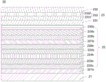
Referring to fig. 4, a second embodiment of the present invention discloses a top-emitting organic electroluminescent element such as a top-emitting OLED. As shown in fig. 4, the top-emission organic electroluminescent element 20 includes, for example: a first electrode 21, an organic functional layer 22 and a second electrode 23.
Here, as shown in fig. 4, the organic functional layer 22 is disposed on the first electrode 21. The second electrode 23 is arranged on the side of the organic functional layer 22 remote from the first electrode 21. The second electrode 23 includes, for example, a work function adjustment layer 231 and a transparent metal oxide layer 232, the work function adjustment layer 231 is located on the side of the organic functional layer 22 away from the first electrode 21, and the transparent metal oxide layer 232 is located on the side of the work function adjustment layer 231 away from the organic functional layer 22.
As shown in fig. 4, the top-emitting organic electroluminescent element 20 disclosed in the present embodiment is different from the top-emitting organic electroluminescent element 10 disclosed in the first embodiment in that the second electrode 23 of the top-emitting organic electroluminescent element 20 disclosed in the present embodiment further includes, for example: the charge generation layer 233 is disposed between the work function adjustment layer 231 and the transparent metal oxide layer 232, wherein the charge generation layer 233 includes, for example, a first type charge generation layer 2331 and a second type charge generation layer 2332, the first type charge generation layer 2331 is disposed on a side of the work function adjustment layer 231 away from the organic functional layer 22, and the second type charge generation layer 2332 is disposed between the first type charge generation layer 2331 and the transparent metal oxide layer 232.
Further, the organic functional layer 22 is, for example, provided on the first electrode 21 and is in contact with the first electrode 21. The second electrode 23 is provided, for example, on a side of the organic functional layer 22 away from the first electrode 21, and is in contact with the organic functional layer 22. The work function adjusting layer 231 is, for example, located on the side of the organic functional layer 22 away from the first electrode 21, and is in contact with the organic functional layer 22. The first-type charge generation layer 2331 is, for example, located on a side of the work function adjusting layer 231 remote from the organic functional layer 22, and is in contact with the work function adjusting layer 231. The second-type charge generation layer 2332 is, for example, located between the first-type charge generation layer 2331 and the transparent metal oxide layer 232, and has one side in contact with the first-type charge generation layer 2331 and the other side in contact with the transparent metal oxide layer 232. The transparent metal oxide layer 232 is, for example, located on the side of the second-type charge generation layer 2332 away from the first-type charge generation layer 2331, and the second-type charge generation layer 2332 is in contact.
The first type charge generation layer 2331 is, for example, n-CGL, and suitable materials include, for example: alkali metals or alkaline earth metals and metal compounds having a low work function include, for example: li, K, Ca, Cs, Mg, LiF, Li2CO3、CsF、Cs2CO3、CsN3Or Rb2CO3And the like.
Further, the first type charge generation layer 2331 is prepared, for example, by a conventional vacuum evaporation process, and the thickness of the first type charge generation layer 2331 ranges from, for example, 2nm to 10 nm.
The second-type charge generation layer 2332 is, for example, p-CGL, and suitable materials are, for example, metal oxides, including: ITO, MoO3、WO3Or V2O5And the like.
Further, the first type charge generation layer 2332 is prepared, for example, by a conventional vacuum evaporation process, and the second type charge generation layer 2332 has a thickness ranging from, for example, 5nm to 20 nm.
The charge generation layer 233 can prevent the work function adjustment layer 231 from being damaged when the transparent metal oxide layer 232 is prepared by a vacuum sputtering process, so that the oxidation damage to the organic material in the organic functional layer 22 is further reduced, and the service life is further prolonged.
Similar to the top-emission organic electroluminescent element 10 disclosed in the first embodiment, the top-emission organic electroluminescent element 20 disclosed in this embodiment may also be a single-color device or a multi-color device, and is widely applicable.
Specifically, as shown in fig. 5, the organic functional layer 22 is, for example, a monochromatic organic functional layer, which includes, for example: a hole injection layer 221a, a hole transport layer 222a, a light emitting layer 223a, an electron transport layer 224a, and an electron injection layer 225a, which are sequentially stacked. The hole injection layer 221a is disposed on the first electrode 21, and is in contact with the first electrode 21. The hole transport layer 222a is provided on the side of the hole injection layer 221a away from the first electrode 21, for example, and is in contact with the hole injection layer 221 a. The light-emitting layer 223a is provided on the side of the hole transport layer 222a away from the hole injection layer 221a, for example, and is in contact with the hole transport layer 222 a. The electron transport layer 224a is provided on the side of the light emitting layer 223a away from the hole transport layer 222a, for example, and is in contact with the light emitting layer 223 a. The electron injection layer 225a is disposed on the side of the electron transport layer 224a away from the light emitting layer 223a, for example, and has one side in contact with the electron transport layer 224a and the other side in contact with the work function adjustment layer 231 of the second electrode 23.
In other embodiments of the present invention, as shown in fig. 6, the organic functional layer 22 is, for example, a multi-color organic functional layer, which includes, for example: a hole injection layer 221b, a hole transport layer 222b, a light emitting layer 223b, and an electron transport layer 224b, an n-type-charge generation layer 225b, a p-type-charge generation layer 226b, a hole transport layer 227b, a light emitting layer 228b, and an electron transport layer 229b and an electron injection layer 230b, which are sequentially stacked. Here, the hole injection transport layer 221b is, for example, disposed on the first electrode 21 and is in contact with the first electrode 21. The hole transport layer 222b is provided, for example, on the side of the hole injection layer 221b away from the first electrode 21, and is in contact with the hole injection layer 221 b. The light-emitting layer 223b is provided, for example, on the side of the hole transport layer 222b remote from the hole injection layer 221b, and is in contact with the hole transport layer 222 b. The electron transport layer 224b is provided, for example, on the side of the light-emitting layer 223b remote from the hole transport layer 222b1, and is in contact with the light-emitting layer 223 b. The n-type charge generation layer 225b is disposed on the side of the electron transport layer 224b away from the light emitting layer 2223b, and is in contact with the electron transport layer 224 b. The p-type-charge generation layer 226b is disposed on the side of the n-type-charge generation layer 225b away from the electron transport layer 224b, and is in contact with the n-type-charge generation layer 225 b. The hole transport layer 227b is disposed on a side of the p-type-charge generation layer 226b away from the n-type-charge generation layer 225b, and is in contact with the p-type-charge generation layer 226 b. The light emitting layer 228b is disposed on a side of the hole transport layer 227b remote from the p-type charge generation layer 226b, and is in contact with the hole transport layer 227 b. The electron transport layer 229b is provided on a side of the light-emitting layer 228b remote from the hole transport layer 227b, and is in contact with the light-emitting layer 228 b. The electron injection layer 230b is provided on the side of the electron transport layer 229b remote from the light-emitting layer 228b, and has one side in contact with the electron transport layer 229b and the other side in contact with the work function adjusting layer 231 of the second electrode 23.
For the first electrode 21, the organic functional layer 22, the work function adjusting layer 231, and the transparent metal oxide layer 232 of the top-emitting organic electroluminescent device 20 disclosed in this embodiment, reference may be made to the first embodiment, and details are not repeated herein for brevity.
In summary, the top-emitting organic electroluminescent device disclosed in this embodiment can improve the efficiency of injecting electrons into the organic functional layer, reduce the turn-on voltage, and improve the light-emitting efficiency, and the generation of the second electrode can be completed by using the existing process, the process is simple and mature, the production cost is controllable, the damage to the work function adjustment layer when the transparent metal oxide layer is manufactured by the vacuum sputtering process can be avoided, the oxidative damage to the organic material in the organic functional layer is reduced, the service life is prolonged, and the top-emitting organic electroluminescent device is suitable for not only a monochromatic OLED but also a multicolor OLED, and has a wide application range.
[ third embodiment ]
Referring to fig. 7, a third embodiment of the present invention discloses a top emission organic electroluminescent device. As shown in fig. 7, the top emission organic electroluminescent device 30 includes, for example: a substrate 31, a drive control circuit layer 32, and a top emission organic electroluminescent element 10 as disclosed in the foregoing first embodiment.
Here, the drive control circuit layer 32 is provided on the substrate 31. The top-emitting organic electroluminescent element 10 is disposed on the side of the drive control circuit layer 32 remote from the substrate 31. The first electrode 11 of the top emission organic electroluminescent element 10 is disposed on the drive control circuit layer 32, the organic functional layer 12 is disposed on the first electrode 11, the second electrode 13 is disposed on a side of the organic functional layer 12 away from the first electrode 11, the second electrode 13 includes, for example, a work function adjusting layer 131 and a transparent metal oxide layer 132, the work function adjusting layer 131 is disposed on a side of the organic functional layer 12 away from the first electrode 11, and the transparent metal oxide layer 132 is disposed on a side of the work function adjusting layer 131 away from the organic functional layer 12.
Specifically, the substrate 31 may be formed of a transparent material. The substrate 31 is, for example, a quartz substrate, an artificial quartz substrate, a calcium fluoride substrate, a fluorine-doped quartz substrate, a soda lime glass substrate, or the like. Alternatively, the substrate 31 may be formed of a flexible transparent material. The substrate 31 is, for example, a polyimide substrate, and may include a first polyimide layer, a barrier film layer, a second polyimide layer, and the like.
The drive control circuit layer 32 includes, for example, a plurality of transistors and a storage capacitor electrically connected to the plurality of transistors. The first electrode 11 is connected to a plurality of transistors. The transistor structure is, for example, a Top Gate (Top Gate), a Back Channel Etch (BCE) structure, an Etch Stop Layer (ESL) structure, or the like. The material of the active layer of the transistor is mentioned as an oxide, a silicon material or an organic substance, for example. Specifically, the material of the active layer includes, for example: amorphous Indium Gallium Zinc Oxide (a-IGZO) material, Zinc oxynitride (ZnON), IZTO, Amorphous silicon (a-Si), low temperature polysilicon (p-Si), hexathiophene, polythiophene, and the like. The materials of the electrodes of the transistor and the leads thereof may be common metal materials, such as silver (Ag), copper (Cu), aluminum (Al), molybdenum (Mo), etc., or alloy materials of the above metals, such as aluminum neodymium alloy (AlNd), molybdenum niobium alloy (MoNb), etc., or multilayer metals, such as MoNb/Cu/MoNb, etc., or may be stack structures of metals and transparent conductive oxides, such as Indium Tin Oxide (ITO), aluminum-doped zinc oxide (AZO), etc., such as Mo/AlNd/ITO, ITO/Ag/ITO, etc. The material of the Buffer, GI, ILD, PVX layer includes dielectric materials such as silicon oxide (SiOx), silicon nitride (SiNx), silicon oxynitride (SiON), or various novel organic insulating materials, or high dielectric constant materials such as aluminum oxide (AlOx), hafnium oxide (HfOx), tantalum oxide (TaOx), etc. The drive control circuit layer 32 is formed by, for example, forming a film, exposing, and etching a film layer of different materials with different patterns superimposed thereon.
For example, as shown in fig. 8, the driving control circuit layer 32 includes, for example, two transistors (321, 323) and a storage capacitor 322 electrically connecting the two transistors. The first electrode of the top-emission organic electroluminescent element 10 is electrically connected to the transistor 321 and the transistor 323. As shown in fig. 8, the positive voltage power ELVDD is supplied to the positive power supply terminal and the ground power supply voltage ELVSS may be supplied to the ground power supply terminal, and the state of the driving transistor 321 controls the amount of current flowing through the top emission organic electroluminescent element 10, thereby controlling the amount of light emitted from the top emission organic electroluminescent device 10. To ensure that the transistor 321 is maintained in a desired state between successive frames of data, the voltage on the storage capacitor 322 is applied to the gate of the transistor 321 at node a to control the transistor 321. Data may be loaded into the storage capacitor 322 using one or more switching transistors, such as transistor 323. When the switching transistor 323 is off, the Data Line (DL) is isolated from the storage capacitor 322 and the gate voltage on node a is equal to the data value stored in the storage capacitor 322. When the gate line, also called a scan line (GL), is turned off, the switching transistor 323 will be turned on and a new data signal on the data line DL will be loaded into the storage capacitor 322. The new signal on the storage capacitance 322 is applied to the gate of the transistor 321 at node a, thereby adjusting the state of the transistor 321 and adjusting the corresponding amount of light emitted by the top-emitting organic electroluminescent element 10.
It should be noted that the present invention does not limit the specific structure of the driving control circuit layer 32. The foregoing and the schematic drawings are only intended to better illustrate the present embodiments.
For the related description of the top-emitting organic electroluminescent device 10, reference may be made to the foregoing first embodiment, and the beneficial effects of the present embodiment are the same as those of the foregoing first embodiment, which are not repeated herein for brevity.
[ fourth example ] A
Referring to fig. 9, a fourth embodiment of the present invention discloses a top emission organic electroluminescent device. As shown in fig. 9, the top emission organic electroluminescent device 40 includes, for example: a substrate 41, a drive control circuit layer 42, and a top emission organic electroluminescent element 20 as disclosed in the foregoing second embodiment.
Here, the drive control circuit layer 42 is provided on the substrate 41. The top-emitting organic electroluminescent element 20 is disposed on a side of the drive control circuit layer 42 remote from the substrate 41. The first electrode 21 of the top emission organic electroluminescent element 20 is disposed on the drive control circuit layer 42, the organic functional layer 22 is disposed on the first electrode 21, the second electrode 23 is disposed on the side of the organic functional layer 22 away from the first electrode 21, the second electrode 23 includes, for example, a work function adjusting layer 231 and a transparent metal oxide layer 232, the work function adjusting layer 231 is disposed on the side of the organic functional layer 22 away from the first electrode 21, the transparent metal oxide layer 232 is disposed on the side of the work function adjusting layer 231 away from the organic functional layer 22, the charge generating layer 233 is disposed between the work function adjusting layer 231 and the transparent metal oxide layer 232, the charge generation layer 233 includes, for example, a first type charge generation layer 2331 and a second type charge generation layer 2332, the first type charge generation layer 2331 is disposed on a side of the work function adjustment layer 231 away from the organic functional layer 22, and the second type charge generation layer 2332 is disposed between the first type charge generation layer 2331 and the transparent metal oxide layer 232.
Specifically, the substrate 41 is formed of, for example, a transparent material. For example, the substrate may be a quartz substrate, an artificial quartz substrate, a calcium fluoride substrate, a fluorine-doped quartz substrate, or a soda lime glass substrate. Alternatively, the substrate may be formed of a flexible transparent material. The substrate is, for example, a polyimide substrate, and may include a first polyimide layer, a barrier film layer, a second polyimide layer, and the like.
The drive control circuit layer 42 includes, for example, a plurality of transistors and capacitors connecting the transistors. The first electrode 21 is connected to a plurality of transistors. The structure of the transistor is, for example, a Top Gate structure (Top Gate), a Back Channel Etch type structure (Back Channel Etch, BCE), or an Etch barrier Layer type structure (Etch Stop Layer, ESL). The material of the active layer of the transistor may be, for example, an oxide, a silicon material, or an organic material. Specifically, the material of the active layer includes, for example: amorphous Indium Gallium Zinc Oxide (a-IGZO) material, Zinc oxynitride (ZnON), IZTO, Amorphous silicon (a-Si), low temperature polysilicon (p-Si), hexathiophene, polythiophene, or the like. The materials of the electrodes of the transistor and the leads thereof may be commonly used metal materials such as silver (Ag), copper (Cu), aluminum (Al), molybdenum (Mo), etc., or alloy materials of the above metals such as aluminum neodymium alloy (AlNd), molybdenum niobium alloy (MoNb), etc., or multi-layer metals such as MoNb/Cu/MoNb, etc., or may be stack structures of metals and transparent conductive oxides such as Indium Tin Oxide (ITO), aluminum-doped zinc oxide (AZO), etc., such as Mo/AlNd/ITO, ITO/Ag/ITO, etc. The material of the Buffer, GI, ILD, PVX layer includes dielectric materials such as silicon oxide (SiOx), silicon nitride (SiNx), silicon oxynitride (SiON), or various novel organic insulating materials, or high dielectric constant materials such as aluminum oxide (AlOx), hafnium oxide (HfOx), tantalum oxide (TaOx), etc. The drive control circuit layer 42 is formed by, for example, laminating film layers of different materials having different patterns by film formation, exposure, and etching.
For a specific structure of the driving control circuit layer 42, reference may be made to the description of the driving control circuit layer 32 of the top-emission organic electroluminescent device 30 disclosed in the foregoing third embodiment, and details thereof are not repeated herein.
For the related description of the top-emitting organic electroluminescent device 20, reference may be made to the foregoing second embodiment, and the beneficial effects of the present embodiment are the same as those of the foregoing second embodiment, which are not repeated herein for brevity.
Finally, it should be noted that: the above examples are only intended to illustrate the technical solution of the present invention, but not to limit it; although the present invention has been described in detail with reference to the foregoing embodiments, it will be understood by those of ordinary skill in the art that: the technical solutions described in the foregoing embodiments may still be modified, or some technical features may be equivalently replaced; and such modifications or substitutions do not depart from the spirit and scope of the corresponding technical solutions of the embodiments of the present invention.
Claims (10)
Priority Applications (2)
| Application Number | Priority Date | Filing Date | Title |
|---|---|---|---|
| CN202010700423.XA CN113964279A (en) | 2020-07-20 | 2020-07-20 | Top-emitting organic electroluminescent element and top-emitting organic electroluminescent device |
| US17/315,482 US11641755B2 (en) | 2020-07-20 | 2021-05-10 | Top-emission type organic electroluminescent element and top-emission type organic electroluminescent device |
Applications Claiming Priority (1)
| Application Number | Priority Date | Filing Date | Title |
|---|---|---|---|
| CN202010700423.XA CN113964279A (en) | 2020-07-20 | 2020-07-20 | Top-emitting organic electroluminescent element and top-emitting organic electroluminescent device |
Publications (1)
| Publication Number | Publication Date |
|---|---|
| CN113964279A true CN113964279A (en) | 2022-01-21 |
Family
ID=79293648
Family Applications (1)
| Application Number | Title | Priority Date | Filing Date |
|---|---|---|---|
| CN202010700423.XA Pending CN113964279A (en) | 2020-07-20 | 2020-07-20 | Top-emitting organic electroluminescent element and top-emitting organic electroluminescent device |
Country Status (2)
| Country | Link |
|---|---|
| US (1) | US11641755B2 (en) |
| CN (1) | CN113964279A (en) |
Cited By (2)
| Publication number | Priority date | Publication date | Assignee | Title |
|---|---|---|---|---|
| CN114864852A (en) * | 2022-07-06 | 2022-08-05 | 京东方科技集团股份有限公司 | Light emitting device and display panel |
| WO2024222333A1 (en) * | 2023-04-26 | 2024-10-31 | 京东方科技集团股份有限公司 | Light-emitting device and method for manufacturing light-emitting device |
Families Citing this family (1)
| Publication number | Priority date | Publication date | Assignee | Title |
|---|---|---|---|---|
| KR20220111814A (en) * | 2021-02-02 | 2022-08-10 | 삼성디스플레이 주식회사 | Display apparatus |
Citations (13)
| Publication number | Priority date | Publication date | Assignee | Title |
|---|---|---|---|---|
| EP1530245A2 (en) * | 2003-11-10 | 2005-05-11 | Junji Kido | Organic electroluminescent devices, organic solar cells, organic fet structures and production method of organic devices |
| US20060027830A1 (en) * | 2004-08-04 | 2006-02-09 | Semiconductor Energy Laboratory Co., Ltd. | Light-emitting element, display device, and electronic appliance |
| TW200803009A (en) * | 2006-03-08 | 2008-01-01 | Semiconductor Energy Lab | Light emitting element, light emitting device, and electronic device |
| CN101427399A (en) * | 2006-04-20 | 2009-05-06 | 出光兴产株式会社 | Organic light emitting element |
| US20100301316A1 (en) * | 2009-05-29 | 2010-12-02 | Semiconductor Energy Laboratory Co., Ltd. | Light-emitting element, light-emitting device, electronic device, and lighting device |
| CN103928631A (en) * | 2013-01-11 | 2014-07-16 | 海洋王照明科技股份有限公司 | Organic electroluminescence apparatus and preparation method thereof |
| CN104051655A (en) * | 2013-03-11 | 2014-09-17 | 海洋王照明科技股份有限公司 | Inverted organic light emission diode device and manufacturing method thereof |
| CN104078622A (en) * | 2013-03-29 | 2014-10-01 | 海洋王照明科技股份有限公司 | Organic light-emitting diode device and manufacturing method thereof |
| CN104183761A (en) * | 2013-05-22 | 2014-12-03 | 海洋王照明科技股份有限公司 | Inverted organic light emission diode and preparation method thereof |
| CN104218165A (en) * | 2014-08-20 | 2014-12-17 | 京东方科技集团股份有限公司 | Organic light-emitting diode device and display device |
| US20150097164A1 (en) * | 2012-05-31 | 2015-04-09 | Lg Chem, Ltd. | Organic light emitting diode |
| US20160254330A1 (en) * | 2013-10-28 | 2016-09-01 | Sharp Kabushiki Kaisha | Organic electroluminescent panel |
| CN206116461U (en) * | 2016-07-22 | 2017-04-19 | 研创应用材料(赣州)股份有限公司 | Adopt OLED rete of low temperature coating film TCO as negative pole |
Family Cites Families (1)
| Publication number | Priority date | Publication date | Assignee | Title |
|---|---|---|---|---|
| JP3933591B2 (en) * | 2002-03-26 | 2007-06-20 | 淳二 城戸 | Organic electroluminescent device |
-
2020
- 2020-07-20 CN CN202010700423.XA patent/CN113964279A/en active Pending
-
2021
- 2021-05-10 US US17/315,482 patent/US11641755B2/en active Active
Patent Citations (16)
| Publication number | Priority date | Publication date | Assignee | Title |
|---|---|---|---|---|
| CN1620212A (en) * | 2003-11-10 | 2005-05-25 | 城户淳二 | Organic devices and organic devices production method |
| EP1530245A2 (en) * | 2003-11-10 | 2005-05-11 | Junji Kido | Organic electroluminescent devices, organic solar cells, organic fet structures and production method of organic devices |
| US20060027830A1 (en) * | 2004-08-04 | 2006-02-09 | Semiconductor Energy Laboratory Co., Ltd. | Light-emitting element, display device, and electronic appliance |
| CN1735298A (en) * | 2004-08-04 | 2006-02-15 | 株式会社半导体能源研究所 | Light emitting elements, display devices and electronic appliances |
| TW200803009A (en) * | 2006-03-08 | 2008-01-01 | Semiconductor Energy Lab | Light emitting element, light emitting device, and electronic device |
| CN101427399A (en) * | 2006-04-20 | 2009-05-06 | 出光兴产株式会社 | Organic light emitting element |
| US20100301316A1 (en) * | 2009-05-29 | 2010-12-02 | Semiconductor Energy Laboratory Co., Ltd. | Light-emitting element, light-emitting device, electronic device, and lighting device |
| US8389979B2 (en) * | 2009-05-29 | 2013-03-05 | Semiconductor Energy Laboratory Co., Ltd. | Light-emitting element, light-emitting device, electronic device, and lighting device |
| US20150097164A1 (en) * | 2012-05-31 | 2015-04-09 | Lg Chem, Ltd. | Organic light emitting diode |
| CN103928631A (en) * | 2013-01-11 | 2014-07-16 | 海洋王照明科技股份有限公司 | Organic electroluminescence apparatus and preparation method thereof |
| CN104051655A (en) * | 2013-03-11 | 2014-09-17 | 海洋王照明科技股份有限公司 | Inverted organic light emission diode device and manufacturing method thereof |
| CN104078622A (en) * | 2013-03-29 | 2014-10-01 | 海洋王照明科技股份有限公司 | Organic light-emitting diode device and manufacturing method thereof |
| CN104183761A (en) * | 2013-05-22 | 2014-12-03 | 海洋王照明科技股份有限公司 | Inverted organic light emission diode and preparation method thereof |
| US20160254330A1 (en) * | 2013-10-28 | 2016-09-01 | Sharp Kabushiki Kaisha | Organic electroluminescent panel |
| CN104218165A (en) * | 2014-08-20 | 2014-12-17 | 京东方科技集团股份有限公司 | Organic light-emitting diode device and display device |
| CN206116461U (en) * | 2016-07-22 | 2017-04-19 | 研创应用材料(赣州)股份有限公司 | Adopt OLED rete of low temperature coating film TCO as negative pole |
Cited By (2)
| Publication number | Priority date | Publication date | Assignee | Title |
|---|---|---|---|---|
| CN114864852A (en) * | 2022-07-06 | 2022-08-05 | 京东方科技集团股份有限公司 | Light emitting device and display panel |
| WO2024222333A1 (en) * | 2023-04-26 | 2024-10-31 | 京东方科技集团股份有限公司 | Light-emitting device and method for manufacturing light-emitting device |
Also Published As
| Publication number | Publication date |
|---|---|
| US11641755B2 (en) | 2023-05-02 |
| US20220020954A1 (en) | 2022-01-20 |
Similar Documents
| Publication | Publication Date | Title |
|---|---|---|
| CN100492651C (en) | Organic electroluminescent device employing multi-layered anode | |
| JP4734368B2 (en) | Organic light emitting display | |
| US9118033B2 (en) | Organic light-emitting diode and display device employing the same | |
| KR100432544B1 (en) | Matrix-Type Three-Terminal Organic EL Display Device | |
| KR100975867B1 (en) | Organic light emitting display | |
| JP4596977B2 (en) | Organic light emitting display | |
| JP4628690B2 (en) | Organic light emitting display | |
| CN109599413B (en) | Display panel and display device | |
| KR20120043001A (en) | Organic electroluminescent element | |
| CN107689422A (en) | Organic light emitting diode and display device including same | |
| CN111584564A (en) | Display panel and display panel manufacturing method | |
| US11641755B2 (en) | Top-emission type organic electroluminescent element and top-emission type organic electroluminescent device | |
| US20140326957A1 (en) | Organic light emitting display device and method of manufacturing the same | |
| US12389738B2 (en) | OLED device, display apparatus and manufacturing method therefor | |
| US7911128B2 (en) | Organic electroluminescence display device having anode and drain sealing structure and a method for fabricating thereof | |
| KR20100022638A (en) | Organic light emitting display | |
| KR101261602B1 (en) | Organic light emitting diode display and manufacturing method thereof | |
| KR20150080153A (en) | Organic Light Emitting Diode And Organic Light Emitting Diode Display Device Including The Same | |
| KR101577833B1 (en) | Organic electroluminescence display device and manufacturing method thereof | |
| KR20070112547A (en) | OLED display and manufacturing method thereof | |
| KR20100021281A (en) | Organic light emitting display device | |
| KR20080102576A (en) | Organic light emitting display | |
| KR101304409B1 (en) | Organic light emitting diode display | |
| WO2025199806A1 (en) | Light-emitting element and display substrate | |
| KR101359914B1 (en) | Organic light emitting device |
Legal Events
| Date | Code | Title | Description |
|---|---|---|---|
| PB01 | Publication | ||
| PB01 | Publication | ||
| SE01 | Entry into force of request for substantive examination | ||
| SE01 | Entry into force of request for substantive examination | ||
| WD01 | Invention patent application deemed withdrawn after publication | ||
| WD01 | Invention patent application deemed withdrawn after publication |
Application publication date: 20220121 |