CN113692650A - Thin film transistor, preparation method thereof, display substrate and display panel - Google Patents
Thin film transistor, preparation method thereof, display substrate and display panel Download PDFInfo
- Publication number
- CN113692650A CN113692650A CN202080000327.2A CN202080000327A CN113692650A CN 113692650 A CN113692650 A CN 113692650A CN 202080000327 A CN202080000327 A CN 202080000327A CN 113692650 A CN113692650 A CN 113692650A
- Authority
- CN
- China
- Prior art keywords
- layer
- thin film
- film transistor
- electrode
- source
- Prior art date
- Legal status (The legal status is an assumption and is not a legal conclusion. Google has not performed a legal analysis and makes no representation as to the accuracy of the status listed.)
- Pending
Links
Images


Classifications
-
- H—ELECTRICITY
- H10—SEMICONDUCTOR DEVICES; ELECTRIC SOLID-STATE DEVICES NOT OTHERWISE PROVIDED FOR
- H10D—INORGANIC ELECTRIC SEMICONDUCTOR DEVICES
- H10D30/00—Field-effect transistors [FET]
- H10D30/60—Insulated-gate field-effect transistors [IGFET]
- H10D30/67—Thin-film transistors [TFT]
- H10D30/6729—Thin-film transistors [TFT] characterised by the electrodes
-
- H—ELECTRICITY
- H10—SEMICONDUCTOR DEVICES; ELECTRIC SOLID-STATE DEVICES NOT OTHERWISE PROVIDED FOR
- H10D—INORGANIC ELECTRIC SEMICONDUCTOR DEVICES
- H10D30/00—Field-effect transistors [FET]
- H10D30/60—Insulated-gate field-effect transistors [IGFET]
- H10D30/67—Thin-film transistors [TFT]
- H10D30/6704—Thin-film transistors [TFT] having supplementary regions or layers in the thin films or in the insulated bulk substrates for controlling properties of the device
-
- H—ELECTRICITY
- H10—SEMICONDUCTOR DEVICES; ELECTRIC SOLID-STATE DEVICES NOT OTHERWISE PROVIDED FOR
- H10D—INORGANIC ELECTRIC SEMICONDUCTOR DEVICES
- H10D64/00—Electrodes of devices having potential barriers
- H10D64/01—Manufacture or treatment
-
- H—ELECTRICITY
- H10—SEMICONDUCTOR DEVICES; ELECTRIC SOLID-STATE DEVICES NOT OTHERWISE PROVIDED FOR
- H10D—INORGANIC ELECTRIC SEMICONDUCTOR DEVICES
- H10D64/00—Electrodes of devices having potential barriers
- H10D64/60—Electrodes characterised by their materials
- H10D64/62—Electrodes ohmically coupled to a semiconductor
-
- H—ELECTRICITY
- H10—SEMICONDUCTOR DEVICES; ELECTRIC SOLID-STATE DEVICES NOT OTHERWISE PROVIDED FOR
- H10D—INORGANIC ELECTRIC SEMICONDUCTOR DEVICES
- H10D99/00—Subject matter not provided for in other groups of this subclass
-
- H—ELECTRICITY
- H10—SEMICONDUCTOR DEVICES; ELECTRIC SOLID-STATE DEVICES NOT OTHERWISE PROVIDED FOR
- H10D—INORGANIC ELECTRIC SEMICONDUCTOR DEVICES
- H10D30/00—Field-effect transistors [FET]
- H10D30/60—Insulated-gate field-effect transistors [IGFET]
- H10D30/67—Thin-film transistors [TFT]
- H10D30/674—Thin-film transistors [TFT] characterised by the active materials
- H10D30/6755—Oxide semiconductors, e.g. zinc oxide, copper aluminium oxide or cadmium stannate
-
- H10P14/6314—
-
- H10P14/6939—
-
- H10P14/69391—
-
- H10P95/00—
Landscapes
- Thin Film Transistor (AREA)
- Engineering & Computer Science (AREA)
- Manufacturing & Machinery (AREA)
Abstract
The application relates to the technical field of display, and discloses a thin film transistor and a preparation method thereof, a display substrate and a display panel, and aims to improve the structure of the thin film transistor, improve the characteristics of the thin film transistor and improve the yield of display products. The thin film transistor includes: a substrate base plate; an active layer on the substrate base plate; the source and drain electrodes are positioned on one side of the active layer, which is far away from the substrate base plate, and comprise an electrode layer and a protective layer, and the material of the electrode layer comprises a first metal element; the protective layer covers the surface of one side, away from the substrate base plate, of the electrode layer and the side face of the electrode layer, and the material of the protective layer is the oxide of the first metal element.
Description
The application relates to the technical field of display, in particular to a thin film transistor, a preparation method thereof, a display substrate and a display panel.
In the field of semiconductor display, in order to meet the development and requirements of large size, high resolution and high driving frequency of a display terminal, a metal material with low resistivity and good electromigration resistance is generally selected as an electrode material, for example, Cu metal is often adopted as a material of a source electrode and a drain electrode of a thin film transistor at present. However, the source and drain electrode metal layer is easily affected by the subsequent manufacturing process, so that the sputtered metal particles are formed and diffused into the active layer, for example, the Plasma (Plasma) bombardment adopted in the passivation layer (PVX) manufacturing process can cause the metal particles of the source and drain electrode to be sputtered onto the channel, thereby causing the transistor characteristic to be conductive, and even causing the whole device to fail.
Disclosure of Invention
The application discloses a thin film transistor and a preparation method thereof, a display substrate and a display panel, and aims to improve the structure of the thin film transistor, improve the characteristics of the thin film transistor and improve the yield of display products.
A thin film transistor, comprising:
a substrate base plate;
an active layer on the substrate base plate;
the source and drain electrodes are positioned on one side of the active layer, which is far away from the substrate base plate, and comprise an electrode layer and a protective layer, and the material of the electrode layer comprises a first metal element; the protective layer covers the surface of one side, away from the substrate base plate, of the electrode layer and the side face of the electrode layer, and the material of the protective layer is the oxide of the first metal element.
Optionally, the source/drain electrode further includes a transition layer located between the active layer and the electrode layer, and an orthographic projection of the transition layer on the substrate is overlapped with an orthographic projection of the electrode layer on the substrate.
Optionally, the protective layer further covers a side surface of the transition layer.
Optionally, the electrode layer is made of an alloy material; the alloy material includes the first metal element therein.
Optionally, the electrode layer material comprises a copper alloy.
Optionally, the first metal element is an aluminum element; the material of the protective layer includes alumina.
Optionally, the first metal element is chromium; the material of the protective layer comprises chromium oxide.
Optionally, the mass percentage of the first metal element in the electrode layer is less than 0.5 wt.%.
Optionally, the ratio of the thickness of the protective layer to the thickness of the electrode layer is 1/20-1/200.
Optionally, the active layer includes an undamaged layer close to the substrate base plate and a damaged layer far from the substrate base plate, and an orthographic projection of the damaged layer on the substrate base plate does not overlap with an orthographic projection of a channel region of the thin film transistor on the substrate base plate.
A display substrate comprising a thin film transistor as claimed in any preceding claim.
A display panel comprises the display substrate.
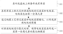
A method for preparing a thin film transistor comprises the following steps:
preparing and forming an active layer on a substrate;
sequentially depositing a transition layer and an electrode layer of a source electrode and a drain electrode on the active layer, wherein the electrode layer comprises a first metal element;
patterning the transition layer and the electrode layer through a composition process to form a pattern of a source drain electrode;
and carrying out oxidation treatment on the source and drain electrodes to form an oxide film layer of the first metal element on the surface of the electrode layer.
Optionally, the electrode layer is a copper alloy, and the first metal element is aluminum or chromium;
oxidizing the source and drain electrodes to form an oxide film layer of a first metal element on the surface of the electrode layer, wherein the method specifically comprises the following steps:
and carrying out thermal annealing treatment on the electrode layer, wherein the annealing temperature is more than or equal to 300 ℃, the annealing time is more than or equal to 1H, and the atmosphere is air, so that an aluminum oxide film layer or a chromium oxide film layer is formed on the surface of the electrode layer.
Optionally, a transition layer and an electrode layer of the source and drain electrodes are sequentially deposited on the active layer, and the method specifically includes:
sequentially depositing a transition layer and an electrode layer by adopting a plasma sputtering deposition process, and forming a damaged layer on the upper surface of the active layer;
patterning the transition layer and the electrode layer through a composition process to form a pattern of a source drain electrode, which specifically comprises the following steps:
and etching the transition layer and the electrode layer by using etching liquid, wherein the etching time Etch time is not less than EPD + A/B, the EPD is the time required for the transition layer and the electrode layer to be etched just, A is the thickness of the damaged layer in the active layer, and B is the etching rate of the etching liquid to the damaged layer in the active layer.
Fig. 1 is a schematic cross-sectional view of a thin film transistor according to an embodiment of the present disclosure;
fig. 2 is a schematic view of a partial cross-sectional structure of a thin film transistor after depositing and forming structures of source and drain electrodes in accordance with an embodiment of the present disclosure;
FIG. 3 is a schematic diagram of a partial cross-sectional structure of the TFT in FIG. 2 after a source/drain electrode pattern is formed by etching;
FIG. 4 is a schematic diagram of a partial cross-sectional structure of the thin film transistor shown in FIG. 3 after a source/drain electrode protection layer is formed by oxidation treatment;
FIG. 5 is a schematic cross-sectional view of a portion of the TFT of FIG. 4 after forming a passivation layer;
fig. 6 is a schematic view of a partial cross-sectional structure of a thin film transistor according to another embodiment of the present disclosure after depositing layers of a source/drain electrode;
FIG. 7 is a schematic cross-sectional view of the thin film transistor shown in FIG. 6 after a source/drain electrode pattern is formed by etching;
fig. 8 is a flowchart illustrating a method for fabricating a thin film transistor according to an embodiment of the present disclosure;
fig. 9 is a schematic diagram comparing characteristic curves of thin film transistors obtained under different source-drain electrode etching time conditions.
In the field of semiconductor Thin Film Transistor (TFT) display, the source and drain electrode metal layers are easily affected by the subsequent fabrication process, so that sputtered metal particles are formed and diffused into the active layer, thereby affecting the device performance. For example, in a passivation layer (PVX) preparation process, Plasma (Plasma) bombardment is adopted, so that metal particles of a source and drain electrode are sputtered, particularly, metal particles are easily sputtered from the side surface of the source and drain electrode and diffused into an active layer, so that the transistor characteristic is conducted, even the whole device fails, generally, the influence is expressed as a normal bright spot in a display product, and the occurrence rate is about 80%. Specifically, metal elements which cause the conduction of the active layer can be obtained through STEM observation and EDX analysis, and for example, a source and drain electrode structure of the TFT adopts B-MoNb/Cu/T-MoNb, and the metal elements generally comprise MO, Nb and Cu.
In view of the above problems, the embodiments of the present application disclose a thin film transistor, a method for manufacturing the thin film transistor, a display substrate, and a display panel, which aim to improve the structure of the thin film transistor, prevent metal particles of source and drain electrodes from splashing to a channel region, reduce poor conduction of a TFT, further improve the characteristics of the thin film transistor, and improve the yield of display products.
The technical solutions in the embodiments of the present application will be clearly and completely described below with reference to the drawings in the embodiments of the present application, and it is obvious that the described embodiments are only a part of the embodiments of the present application, and not all of the embodiments. All other embodiments, which can be derived by a person skilled in the art from the embodiments given herein without making any creative effort, shall fall within the protection scope of the present application.
As shown in fig. 1, 4 and 5, an embodiment of the present application provides a thin film transistor, including:
a base substrate 1;
an active layer 2 on the base substrate 1;
the source-drain electrode 3 is positioned on one side of the active layer 2, which is far away from the substrate base plate 1, and comprises an electrode layer 31 and a protective layer 32, wherein the material of the electrode layer 31 comprises a first metal element; the protective layer 32 covers a surface (upper surface) of the electrode layer 31 on a side away from the base substrate 1 and a side surface of the electrode layer 31, and the material of the protective layer 32 is an oxide of the first metal element.
In particular, reference to the 'side' of the layer structure in this application is to the part of the surface lying between the upper and lower surfaces of the layer structure, or the surface of the layer structure extending in the direction of its thickness.
In the thin film transistor, the source and drain electrodes 3 include the electrode layer 31 and the protective layer 32, wherein the protective layer 32 is made of an oxide of a metal element, and the protective layer 32 covers the upper surface of the electrode layer 31 and the side surface of the electrode layer 31, that is, the protective layer 32 is a dense metal oxide covering the outer surface of the electrode layer 31, so that the electrode layer 31 of the source and drain electrodes 3 can be completely protected by the protective layer 32 in a subsequent process (for example, in a preparation process of the passivation layer 4), on one hand, the electrode layer 31 can be prevented from being further oxidized in the subsequent process, on the other hand, the problem of conductor change of TFT characteristics caused by the fact that metal of the electrode layer 31 is splashed onto the active layer 2 due to a Plasma (Plasma) bombardment process of the subsequent process can be avoided, and therefore, the yield of the TFT can be improved. In addition, the material of the electrode layer 31 of the source/drain electrode 3 includes a first metal element, and the material of the protective layer 32 is an oxide of the first metal element, and further, a manner of directly performing oxidation treatment (for example, high-temperature annealing treatment) on the electrode layer 31 of the source/drain electrode 3 may be adopted to obtain the structure of the protective layer 32, and a preparation process such as Plasma (Plasma) deposition is not required, so that the formation process of the protective layer 32 does not cause metal sputtering of the electrode layer 31, and the problems of TFT characteristic conductor formation and the like may be avoided.
In summary, in the thin film transistor, the oxide protection layer of the first metal element is formed on the surface of the electrode layer of the source and drain electrodes, so that metal particles of the source and drain electrodes can be prevented from being splashed to the TFT channel region, poor conductor formation of the TFT is reduced, characteristics of the thin film transistor are improved, and display product yield is improved.
In some embodiments, the ratio of the thickness of the passivation layer 32 to the thickness of the electrode layer 31 may be 1/20-1/200.
Illustratively, the electrode layer 31 may have a thickness of 200nm to 1000nm, and the protective layer 32 may have a thickness of 5nm to 20 nm.
As shown in fig. 1, 4 and 5, in some embodiments, the source-drain electrode 3 further includes a transition layer 33, the transition layer 33 is located between the active layer 2 and the electrode layer 31, and an orthogonal projection of the transition layer 33 on the substrate base plate 1 overlaps an orthogonal projection of the electrode layer 31 on the substrate base plate 1.
Specifically, the material of the transition layer 33 includes a refractory metal such as titanium (Ti) or molybdenum (Mo), or a metal alloy such as molybdenum niobium alloy (MoNb) or molybdenum titanium nickel (MTD).
Specifically, the electrode layer 31 of the source/drain electrode 3 is generally made of a metal material with low resistivity and good electromigration resistance, such as copper (Cu), so that the adhesion between the electrode layer 31 and the film layer of the deposition substrate is poor, and by arranging the transition layer 33, the adhesion between the source/drain electrode 3 and the deposition substrate can be improved, and the yield of the TFT can be improved. In addition, the transition layer 33 is located on one side of the electrode layer 31 close to the substrate base plate 1, and the transition layer 33 can prevent the surface of one side of the electrode layer 31 close to the substrate base plate 1 from being oxidized to form an oxide layer, so that the transfer efficiency of carriers is ensured, and the yield of the TFT is improved.
As shown in fig. 4 and fig. 5, in some embodiments, in the source/drain electrode 3, the protection layer 32 may also cover the side surface of the transition layer 33, so as to prevent the side surface of the transition layer 33 from sputtering metal onto the active layer 2 during the Plasma (Plasma) bombardment process in the subsequent process, which may cause the TFT characteristic conductance problem.
Specifically, the thickness (generally 10nm to 30nm) of the transition layer 33 is relatively thin, which is only a few tenths of the thickness of the electrode layer 31, and the area of the side surface is small, and in the process of preparing and forming the protection layer 32, the process conditions of oxidation treatment (for example, the conditions of high-temperature annealing treatment) on the electrode layer 31 can be adjusted, so that the first metal element in the electrode layer 31 can be diffused to the side surface of the transition layer 33, and an oxide layer is formed on the side surface of the transition layer 33, thereby achieving the effect that the protection layer 32 covers the outer surfaces of the electrode layer 31 and the transition layer 33 at the same time.
In some embodiments, the electrode layer 31 is an alloy material; the alloy material includes a first metal element.
Illustratively, the material of the electrode layer 31 includes a copper alloy, i.e., an alloy material having copper metal as a main element. Of course, the electrode layer 31 may be an alloy with other metals as the main elements, which are generally required to have a lower resistivity and a good electromigration resistance.
Specifically, the first metal element may be an alloy element in the alloy material, and is generally selected to be a metal element that is easily diffused and easily oxidized.
Illustratively, the first metal element may be specifically aluminum (Al) element, and the material of the protective layer 32 includes aluminum oxide (Al2O 3). For example, the electrode layer 31 may be a copper aluminum alloy (CuAl) and the protective layer 32 may be an aluminum oxide (Al2O3) film.
Illustratively, the first metal element may specifically be chromium (Cr); the material of the protective layer 32 includes chromium oxide. For example, the electrode layer 31 may be a copper chromium alloy (CuCr) and the protective layer 32 may be a chromium oxide film layer.
Specifically, the transition layer and the electrode layer of the conventional source/drain electrode have poor adhesion with the Photoresist (PR), and can be etched after etching, and photoresist stripping (PR Peeling) can be generated when the etching is serious, so that the manufacturing yield and performance of the whole thin film transistor are affected. In the embodiment of the present application, as shown in fig. 2 and fig. 3, the layer structure on which the source/drain electrode 3 is patterned includes the transition layer 33 and the electrode layer 31 stacked in sequence, and the electrode layer 31 above is made of an alloy material and has a good adhesion with the PR, so that the problem of etching or PR Peeling during etching can be avoided, and thus the manufacturing yield and performance of the whole thin film transistor can be improved.
Specifically, the electrode layer 31 is made of an alloy material, such as a copper alloy, and the alloy elements thereof include a first metal element, such as aluminum (Al), chromium (Cr); by utilizing the self-diffusion characteristic of the alloy elements in the alloy material, in the thermal annealing process, as shown in fig. 3 and 4, the first metal element can be gathered or diffused to the surface and interface of the electrode to form a compact oxide layer, i.e. a protective layer 32 is formed, so that the electrode layer 31 of the source/drain electrode 3 is protected, and the problem of TFT (thin film transistor) characteristic conductor formation caused by the fact that the metal of the electrode layer 31 is splashed onto the active layer 2 in the plasma bombardment process of the subsequent process is avoided.
In some embodiments, the mass percent of the alloying element may be set to less than 0.5 wt.% in view of the effect of the alloying element in the alloy material on the resistivity of the entire alloy material. For example, the mass percent of the first metallic element in the alloy material is less than 0.5 wt.%.
As shown in fig. 7, in some embodiments, the active layer 2 includes an undamaged layer 21 close to the substrate base plate 1 and a damaged layer 22 far from the substrate base plate 1, and an orthographic projection of the damaged layer 22 on the substrate base plate 1 does not overlap with an orthographic projection of the channel region 20 of the thin film transistor on the substrate base plate 1.
Specifically, as shown In fig. 6, when the source/drain electrode 3 layer structure (SD deposition) is deposited after the active layer (oxide semiconductor layer, OS)2 is formed, In — O bonds In the OS are broken by the bombardment of Plasma (Plasma), a damaged layer 22(Damage layer) is formed on the surface of the OS, an oxygen vacancy (Vo) is generated, and Vo and H In the OS thin film form VoH, which causes negative shift (shift) of the threshold voltage (Vth) of the oxide thin film transistor, and thus, a conductor is formed. In the present application, the orthographic projection of the damaged layer 22 does not overlap with the orthographic projection of the channel region 20, that is, the overlapped portion of the damaged layer 22 and the channel region 20 is completely etched away, so that the problem of the oxide thin film crystal property conductibility caused by the damaged layer 22 can be avoided.
Specifically, the overlapping portion of the damage layer 22 and the channel region 20 may be completely etched away during the etching of the source-drain electrode 3, thereby simplifying the manufacturing process.
Specifically, as shown in fig. 5, the thin film transistor provided in the embodiment of the present disclosure may further include a Gate (Gate)5, a Gate insulating layer (GI)6, a passivation layer 4, and other structures, which are conventional structures in the thin film transistor and are not described herein again.
Specifically, in the thin film transistor provided in the embodiment of the present application, the substrate may be flexible or rigid. The material for the gate electrode may be a metal such as Mo, Al, Cu, or an alloy of the above metals. The active layer may be an oxide semiconductor such as IGZO, IZO, GZO, or the like, and may have a single-layer, stacked, or multi-layer structure. The SD electrode can be a multilayer composite structure, such as MoNb/CuAl/Al2O3, MoNb/CuCr/CrOx, and the like. Of course, the above materials are merely examples, and the materials of the respective layers are not limited thereto, and may be determined according to actual needs.
The embodiment of the application also provides a display substrate, and the display substrate comprises any one of the thin film transistors.
The embodiment of the application also provides a display panel, which comprises the display substrate and an opposite substrate.
For example, the display panel may be an LCD, the display substrate is an array substrate, and the opposite substrate is a color film substrate.
Alternatively, the display panel may be an OLED, the display substrate may be a driving backplane, and the opposite substrate may be a protection cover plate.
The embodiment of the application also provides a display device which comprises the display panel.
Specifically, the display device can be applied to various electronic devices such as televisions, displays, tablet computers and smart phones.
In addition, based on the thin film transistor provided by the present application, the present application also provides a method for manufacturing a thin film transistor, as shown in fig. 8, the method includes:
In some embodiments, the electrode layer is a copper alloy and the first metal element is aluminum or chromium.
and carrying out thermal annealing treatment on the electrode layer, wherein the annealing temperature is more than or equal to 300 ℃, the annealing time is more than or equal to 1H, and the atmosphere is air, so that an aluminum oxide film layer or a chromium oxide film layer is formed on the surface of the electrode layer.
Specifically, by utilizing the self-diffusion characteristic of the alloy element in the alloy material, in the thermal annealing process, as shown in fig. 3 and 4, the first metal element (aluminum or chromium) in the copper alloy can be gathered or diffused towards the electrode surface and the interface to form a dense oxide layer, i.e., a protective layer 32 is formed, so that the protection of the source/drain electrode 3 and the electrode layer 31 is realized, and the problem of conductor of the TFT characteristics caused by the fact that the metal of the electrode layer 31 is splashed onto the active layer 2 in the plasma bombardment process of the subsequent process is avoided.
In some embodiments, step 102, sequentially depositing a transition layer and an electrode layer of a source drain electrode on an active layer, specifically including:
as shown in fig. 6, the transition layer 33 and the electrode layer 31 are sequentially deposited using a plasma sputter deposition process while forming the damage layer 22 on the upper surface of the active layer 2.
Further, in step 103, patterning the transition layer and the electrode layer by a patterning process to form a pattern of a source/drain electrode, which specifically includes:
as shown in fig. 7, the transition layer 33 and the electrode layer 31 are etched by using an etching solution, and the etching time Etch time is greater than or equal to EPD + a/B, where EPD is the time required for the transition layer 33 and the electrode layer 31 to be etched, a is the thickness (dam layer Depth) of the damaged layer 22 in the active layer 2, and B is the etching rate of the etching solution to the damaged layer 22 in the active layer 2.
Specifically, as shown In fig. 6, when the source/drain electrode 3 layer structure (SD deposition) is deposited after the active layer (oxide semiconductor layer, OS)2 is formed, In — O bonds In the OS are broken by the bombardment of Plasma (Plasma), a damaged layer 22(Damage layer) is formed on the surface of the OS, an oxygen vacancy (Vo) is generated, and Vo and H In the OS thin film form VoH, which causes negative shift (shift) of the threshold voltage (Vth) of the oxide thin film transistor, and thus, a conductor is formed.
In the application, the etching time of the source and drain electrodes is set so as to form a standard etching specification. Specifically, in the present application, the EPD is a time required for the transition layer and the electrode layer to be just etched, that is, a time for forming the source and drain electrode patterns by just etching, and by using the parameters a and B, an Over Etch time is obtained as a/B, that is, a time required for further etching the damaged layer in the active layer. By setting the actual etching time in the etching process of the source and drain electrodes (SD) to be more than or equal to EPD + A/B, the OS Damage layer can be thoroughly removed while the source and drain electrodes are etched, so that the problem of conductor of the characteristics of the oxide thin film transistor is solved, and the performance of the oxide thin film transistor can be greatly improved.
Illustratively, the EPD is a time for a source/drain electrode structure to be etched, and is determined by properties (thickness, film quality, etc.) of a source/drain electrode film layer and an etching solution system, and can be obtained by analyzing experimental data. In the related art, the time (EPD) for completing the etching of the source-drain electrode structure is a conventional parameter, and is not described herein again.
For example, for the parameter a (dam layer depth), the deposition power, time, deposition thickness, and the like of the transition layer (e.g., MoNb) at the bottom of the source/drain electrode are generally related, and generally, the higher the deposition power, the longer the deposition time, the thicker the deposition thickness, the larger a of the transition layer; specifically, the parameter a can be calculated by testing the sheet resistance of OS, SIMS, TEM, and the like.
Illustratively, the parameter B (dam layer E/R) is generally related to the density of the etching solution and the active layer pattern material, and can be obtained through experimental data analysis.
Specifically, in this embodiment, the active layer material is IGZO, the transition layer material of the source/drain electrode is MoNb, and the electrode layer material is Cu. Taking the SD etching solution as an example, H2O2 series Cu etching solution containing F, F ions can corrode OS, and the OS Damage layer is thoroughly removed while SD etching is carried out. Under the conditions of this embodiment, EPD is 73s,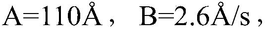 the Over Etch time is 110/2.6 42 s/a/B. Further, EPD + a/B is 73s +42s is 115 s. In an actual process, the actual etching time is controlled according to the standard that the Etch time is not less than EPD + A/B-115 s, that is, the OS Damage layer of the channel region can be completely removed by etching.
Fig. 9 is a TFT characteristic curve obtained by different etching times under the conditions of this embodiment. Specifically, the four graphs in fig. 9 are characteristic curves of TFTs in the display substrate obtained by using four etching time conditions of 100s, 110s, 115s, and 120s, where A, B, C, D four curves included in each graph are characteristic curves of TFTs at four different positions of the display substrate, respectively, and due to the limitation of the actual etching process, the etching depths at the different positions of the display substrate are different, so that the TFT characteristics at the different positions are different, and fig. 9 specifically shows characteristic curves A, B, C, D of TFTs at four representative positions, so as to fully illustrate the TFT characteristics of the entire display substrate. It can be seen by comparing the characteristic curves in the above four graphs that the TFT characteristic results obtained by different etching times are different, specifically, as the etching time is lengthened, the trend of the conductor formation of the TFT characteristic in the display substrate is weakened, and when the actual etching time Etch time is greater than or equal to 115s, as in the case of 115s and 120s in fig. 9, the TFT characteristics of each part in the display substrate can be normal, which is identical to the established standard of the above etching time set in the embodiment of the present application. Therefore, by using the etching time of the source/drain electrode (SD) as the standard provided in this embodiment, the OS Damage layer of the TFT at each portion of the display substrate can be completely removed while the source/drain electrode is etched, thereby solving the problem of the electrical conductivity of the oxide thin film transistor, and greatly improving the performance of the display substrate.
For example, the method for manufacturing a thin film transistor provided in the embodiment of the present application may further include the steps of manufacturing a gate electrode, a gate insulating layer, a passivation layer, and the like, and the overall process may generally include: as shown in fig. 5, a Gate (Gate)5, a Gate insulating layer (GI)6, an Active layer (Active)2, a metal source drain electrode (SD)3, and a passivation layer 4 are sequentially formed on a substrate 1.
Specifically, in the thin film transistor provided in the embodiment of the present application, the substrate may be flexible or rigid. The material for the gate electrode may be a metal such as Mo, Al, Cu, or an alloy of the above metals. The active layer may be an oxide semiconductor such as IGZO, IZO, GZO, or the like, and may have a single-layer, stacked, or multi-layer structure. The SD electrode can be a multilayer composite structure, such as MoNb/CuAl/Al2O3, MoNb/CuCr/CrOx, and the like. Of course, the above materials are merely examples, and the materials of the respective layers are not limited thereto, and may be determined according to actual needs.
It should be noted that, in some embodiments of the present disclosure, the method for manufacturing the thin film transistor may further include more steps, which may be determined according to actual requirements, and the embodiments of the present disclosure are not limited thereto. In addition, in the method for manufacturing a thin film transistor provided in the embodiment of the present disclosure, the specific process and the manufacturing process of steps 102, 103, and 104 are not limited to the above-mentioned embodiments, and other process manners and steps may also be used for manufacturing, and reference may be specifically made to the description of each layer structure in the thin film transistor, and details are not described here.
It will be apparent to those skilled in the art that various changes and modifications may be made in the embodiments of the present application without departing from the spirit and scope of the application. Thus, if such modifications and variations of the present application fall within the scope of the claims of the present application and their equivalents, the present application is intended to include such modifications and variations as well.
Claims (15)
Applications Claiming Priority (1)
| Application Number | Priority Date | Filing Date | Title |
|---|---|---|---|
| PCT/CN2020/080260 WO2021184312A1 (en) | 2020-03-19 | 2020-03-19 | Thin-film transistor and preparation method therefor, and display substrate and display panel |
Publications (1)
| Publication Number | Publication Date |
|---|---|
| CN113692650A true CN113692650A (en) | 2021-11-23 |
Family
ID=77767965
Family Applications (1)
| Application Number | Title | Priority Date | Filing Date |
|---|---|---|---|
| CN202080000327.2A Pending CN113692650A (en) | 2020-03-19 | 2020-03-19 | Thin film transistor, preparation method thereof, display substrate and display panel |
Country Status (4)
| Country | Link |
|---|---|
| US (1) | US12501719B2 (en) |
| EP (1) | EP4113628A4 (en) |
| CN (1) | CN113692650A (en) |
| WO (1) | WO2021184312A1 (en) |
Families Citing this family (1)
| Publication number | Priority date | Publication date | Assignee | Title |
|---|---|---|---|---|
| WO2024216554A1 (en) * | 2023-04-19 | 2024-10-24 | 京东方科技集团股份有限公司 | Display substrate, preparation method therefor, and display apparatus |
Citations (7)
| Publication number | Priority date | Publication date | Assignee | Title |
|---|---|---|---|---|
| CN102648526A (en) * | 2009-12-04 | 2012-08-22 | 株式会社半导体能源研究所 | Semiconductor device and manufacturing method thereof |
| WO2012141089A1 (en) * | 2011-04-11 | 2012-10-18 | 株式会社日立製作所 | Display device and method for manufacturing same |
| CN103227206A (en) * | 2012-01-26 | 2013-07-31 | 日立电线株式会社 | A thin film transistor, a manufacturing method thereof, and a display apparatus using the same |
| US20150155362A1 (en) * | 2013-11-29 | 2015-06-04 | Semiconductor Energy Laboratory Co., Ltd. | Semiconductor device and method for manufacturing the same |
| JP2015119174A (en) * | 2013-11-15 | 2015-06-25 | 株式会社半導体エネルギー研究所 | Semiconductor device and display device |
| US20160197192A1 (en) * | 2015-01-02 | 2016-07-07 | Samsung Display Co., Ltd. | Thin film transistor array panel and method of manufacturing the same |
| CN107004719A (en) * | 2014-11-28 | 2017-08-01 | 夏普株式会社 | Semiconductor device and its manufacture method |
Family Cites Families (12)
| Publication number | Priority date | Publication date | Assignee | Title |
|---|---|---|---|---|
| KR100623816B1 (en) * | 2002-12-26 | 2006-09-18 | 엘지.필립스 엘시디 주식회사 | Black matrix forming method and liquid crystal display device using same |
| KR101308437B1 (en) * | 2006-08-03 | 2013-09-16 | 엘지디스플레이 주식회사 | Method for manufacturing of liquid crystal display |
| KR100858088B1 (en) * | 2007-02-28 | 2008-09-10 | 삼성전자주식회사 | Thin film transistor and method of manufacturing the same |
| JP5171990B2 (en) * | 2011-05-13 | 2013-03-27 | 株式会社神戸製鋼所 | Cu alloy film and display device |
| CN102386237A (en) | 2011-11-23 | 2012-03-21 | 深圳市华星光电技术有限公司 | Thin-film transistor, array substrate and device and preparation method |
| US20130126870A1 (en) | 2011-11-23 | 2013-05-23 | Hao Kou | Thin Film Transistor, Array Substrate, Device and Manufacturing Method |
| US9054204B2 (en) * | 2012-01-20 | 2015-06-09 | Sony Corporation | Thin-film transistor, method of manufacturing the same, display unit, and electronic apparatus |
| JP6015389B2 (en) * | 2012-11-30 | 2016-10-26 | 株式会社リコー | Field effect transistor, display element, image display device, and system |
| KR102089314B1 (en) | 2013-05-14 | 2020-04-14 | 엘지디스플레이 주식회사 | Oxide thin film transistor and method of fabricating the same |
| US9991392B2 (en) | 2013-12-03 | 2018-06-05 | Semiconductor Energy Laboratory Co., Ltd. | Semiconductor device and manufacturing method thereof |
| CN105097950A (en) * | 2015-08-24 | 2015-11-25 | 京东方科技集团股份有限公司 | Thin film transistor and manufacturing method thereof, array substrate, and display device |
| US10916661B2 (en) * | 2016-11-28 | 2021-02-09 | Merck Patent Gmbh | Thin film transistor substrate provided with protective film and method for producing same |
-
2020
- 2020-03-19 CN CN202080000327.2A patent/CN113692650A/en active Pending
- 2020-03-19 WO PCT/CN2020/080260 patent/WO2021184312A1/en not_active Ceased
- 2020-03-19 EP EP20926348.2A patent/EP4113628A4/en active Pending
- 2020-03-19 US US17/905,246 patent/US12501719B2/en active Active
Patent Citations (7)
| Publication number | Priority date | Publication date | Assignee | Title |
|---|---|---|---|---|
| CN102648526A (en) * | 2009-12-04 | 2012-08-22 | 株式会社半导体能源研究所 | Semiconductor device and manufacturing method thereof |
| WO2012141089A1 (en) * | 2011-04-11 | 2012-10-18 | 株式会社日立製作所 | Display device and method for manufacturing same |
| CN103227206A (en) * | 2012-01-26 | 2013-07-31 | 日立电线株式会社 | A thin film transistor, a manufacturing method thereof, and a display apparatus using the same |
| JP2015119174A (en) * | 2013-11-15 | 2015-06-25 | 株式会社半導体エネルギー研究所 | Semiconductor device and display device |
| US20150155362A1 (en) * | 2013-11-29 | 2015-06-04 | Semiconductor Energy Laboratory Co., Ltd. | Semiconductor device and method for manufacturing the same |
| CN107004719A (en) * | 2014-11-28 | 2017-08-01 | 夏普株式会社 | Semiconductor device and its manufacture method |
| US20160197192A1 (en) * | 2015-01-02 | 2016-07-07 | Samsung Display Co., Ltd. | Thin film transistor array panel and method of manufacturing the same |
Also Published As
| Publication number | Publication date |
|---|---|
| EP4113628A1 (en) | 2023-01-04 |
| US20230110228A1 (en) | 2023-04-13 |
| US12501719B2 (en) | 2025-12-16 |
| EP4113628A4 (en) | 2023-04-26 |
| WO2021184312A1 (en) | 2021-09-23 |
Similar Documents
| Publication | Publication Date | Title |
|---|---|---|
| CN101814455B (en) | Method for manufacturing array substrate | |
| US7071037B2 (en) | Semiconductor device and manufacturing method thereof | |
| US20150295092A1 (en) | Semiconductor device | |
| US8847228B2 (en) | Thin film transistor array panel | |
| EP3093888B1 (en) | Method of fabricating a thin film transistor | |
| US9831350B2 (en) | Thin film transistor and method of manufacturing the same | |
| JP2007157916A (en) | TFT substrate and manufacturing method of TFT substrate | |
| WO2014020892A1 (en) | Thin film transistor and method for manufacturing same | |
| KR101484063B1 (en) | Thin film transistor array panel and method of fabricating the same | |
| WO2016061715A1 (en) | Method for fabricating metallic oxide thin film transistor | |
| US20140175423A1 (en) | Thin film transistor array panel and method of manufacturing the same | |
| CN107968097B (en) | Display device, display substrate and manufacturing method thereof | |
| KR102080484B1 (en) | Array substrate for Liquid crystal display device and Method for manufacturing the same | |
| TWI527118B (en) | Method for manufacturing film and display metal wire thin film transistor array panel using the same and manufacturing method of the same | |
| JP2007053363A (en) | Wiring, method for forming the same, thin film transistor substrate, and method for manufacturing the same | |
| JP2007053363A5 (en) | ||
| EP3261127A1 (en) | Thin-film transistor and manufacturing method therefor, array substrate and display device | |
| KR20130039945A (en) | Thin film transistor array panel and manufacturing method thereof | |
| CN108766972A (en) | Thin film transistor and its manufacturing method, display base plate | |
| CN113692650A (en) | Thin film transistor, preparation method thereof, display substrate and display panel | |
| US10475822B2 (en) | Array substrate, display panel and display apparatus having the same, and fabricating method thereof | |
| WO2016058312A1 (en) | Thin film transistor and manufacturing method therefor, display substrate and display device | |
| CN106252203A (en) | Crystallization method and semiconductor structure of metal oxide semiconductor layer | |
| WO2018192210A1 (en) | Conductive pattern structure and preparation method therefor, and array substrate and display device | |
| WO2016192447A1 (en) | Array substrate and method for fabrication thereof and display device |
Legal Events
| Date | Code | Title | Description |
|---|---|---|---|
| PB01 | Publication | ||
| PB01 | Publication | ||
| SE01 | Entry into force of request for substantive examination | ||
| SE01 | Entry into force of request for substantive examination | ||
| RJ01 | Rejection of invention patent application after publication |
Application publication date: 20211123 |
|
| RJ01 | Rejection of invention patent application after publication |