CN113691132B - Voltage balance three-state double-output boost converter and control method thereof - Google Patents
Voltage balance three-state double-output boost converter and control method thereof Download PDFInfo
- Publication number
- CN113691132B CN113691132B CN202110960830.9A CN202110960830A CN113691132B CN 113691132 B CN113691132 B CN 113691132B CN 202110960830 A CN202110960830 A CN 202110960830A CN 113691132 B CN113691132 B CN 113691132B
- Authority
- CN
- China
- Prior art keywords
- output
- switching tube
- switch tube
- tube
- dead time
- Prior art date
- Legal status (The legal status is an assumption and is not a legal conclusion. Google has not performed a legal analysis and makes no representation as to the accuracy of the status listed.)
- Expired - Fee Related
Links
- 238000000034 method Methods 0.000 title claims abstract description 22
- 239000003990 capacitor Substances 0.000 claims description 34
- 238000004146 energy storage Methods 0.000 claims description 20
- 230000000295 complement effect Effects 0.000 claims description 7
- 230000009977 dual effect Effects 0.000 claims 2
- 238000004088 simulation Methods 0.000 description 11
- 238000004458 analytical method Methods 0.000 description 6
- 230000003111 delayed effect Effects 0.000 description 4
- 230000014509 gene expression Effects 0.000 description 4
- 238000004364 calculation method Methods 0.000 description 3
- 238000010586 diagram Methods 0.000 description 3
- NAWXUBYGYWOOIX-SFHVURJKSA-N (2s)-2-[[4-[2-(2,4-diaminoquinazolin-6-yl)ethyl]benzoyl]amino]-4-methylidenepentanedioic acid Chemical compound C1=CC2=NC(N)=NC(N)=C2C=C1CCC1=CC=C(C(=O)N[C@@H](CC(=C)C(O)=O)C(O)=O)C=C1 NAWXUBYGYWOOIX-SFHVURJKSA-N 0.000 description 2
- 238000005516 engineering process Methods 0.000 description 2
- 238000011160 research Methods 0.000 description 2
- 230000009286 beneficial effect Effects 0.000 description 1
- 238000010276 construction Methods 0.000 description 1
- 238000013461 design Methods 0.000 description 1
- 238000011161 development Methods 0.000 description 1
- 238000011835 investigation Methods 0.000 description 1
- 238000012423 maintenance Methods 0.000 description 1
- 238000010248 power generation Methods 0.000 description 1
- 230000002028 premature Effects 0.000 description 1
- 230000000630 rising effect Effects 0.000 description 1
Images


Classifications
-
- H—ELECTRICITY
- H02—GENERATION; CONVERSION OR DISTRIBUTION OF ELECTRIC POWER
- H02M—APPARATUS FOR CONVERSION BETWEEN AC AND AC, BETWEEN AC AND DC, OR BETWEEN DC AND DC, AND FOR USE WITH MAINS OR SIMILAR POWER SUPPLY SYSTEMS; CONVERSION OF DC OR AC INPUT POWER INTO SURGE OUTPUT POWER; CONTROL OR REGULATION THEREOF
- H02M3/00—Conversion of DC power input into DC power output
- H02M3/02—Conversion of DC power input into DC power output without intermediate conversion into AC
- H02M3/04—Conversion of DC power input into DC power output without intermediate conversion into AC by static converters
- H02M3/10—Conversion of DC power input into DC power output without intermediate conversion into AC by static converters using discharge tubes with control electrode or semiconductor devices with control electrode
- H02M3/145—Conversion of DC power input into DC power output without intermediate conversion into AC by static converters using discharge tubes with control electrode or semiconductor devices with control electrode using devices of a triode or transistor type requiring continuous application of a control signal
- H02M3/155—Conversion of DC power input into DC power output without intermediate conversion into AC by static converters using discharge tubes with control electrode or semiconductor devices with control electrode using devices of a triode or transistor type requiring continuous application of a control signal using semiconductor devices only
- H02M3/156—Conversion of DC power input into DC power output without intermediate conversion into AC by static converters using discharge tubes with control electrode or semiconductor devices with control electrode using devices of a triode or transistor type requiring continuous application of a control signal using semiconductor devices only with automatic control of output voltage or current, e.g. switching regulators
- H02M3/158—Conversion of DC power input into DC power output without intermediate conversion into AC by static converters using discharge tubes with control electrode or semiconductor devices with control electrode using devices of a triode or transistor type requiring continuous application of a control signal using semiconductor devices only with automatic control of output voltage or current, e.g. switching regulators including plural semiconductor devices as final control devices for a single load
- H02M3/1584—Conversion of DC power input into DC power output without intermediate conversion into AC by static converters using discharge tubes with control electrode or semiconductor devices with control electrode using devices of a triode or transistor type requiring continuous application of a control signal using semiconductor devices only with automatic control of output voltage or current, e.g. switching regulators including plural semiconductor devices as final control devices for a single load with a plurality of power processing stages connected in parallel
Landscapes
- Engineering & Computer Science (AREA)
- Power Engineering (AREA)
- Dc-Dc Converters (AREA)
Abstract
本发明提供一种电压均衡三态双输出升压变换器及其控制方法,属于非隔离变换器技术领域。该方案基于输入并联输出串联变换器,通过添加辅助平衡支路构建新的变换器拓扑,并根据死区时间大小关系或两个输出电压大小关系,控制对应的开关管导通时序,创建新的电路模态(第三态)、改变电感的伏秒平衡,从而解决死区时间不一致带来的电压不均衡问题。
The invention provides a voltage balanced three-state double-output boost converter and a control method thereof, belonging to the technical field of non-isolated converters. This scheme is based on the input parallel output series converter, and constructs a new converter topology by adding an auxiliary balancing branch, and controls the corresponding switching tube turn-on timing according to the relationship between the dead time or the relationship between the two output voltages to create a new The circuit mode (third state) changes the volt-second balance of the inductor to solve the problem of voltage imbalance caused by inconsistent dead time.
Description
技术领域technical field
本发明属于非隔离变换器技术领域,具体涉及一种电压均衡三态双输出升压变换器及其控制方法。The invention belongs to the technical field of non-isolated converters, and in particular relates to a voltage balanced three-state double-output boost converter and a control method thereof.
背景技术Background technique
随着分布式发电系统和可再生能源的发展,应用于可再生能源和双极直流微网之间的并网技术也得到越来越多的关注,在该应用中的变换器也得到了越来越多的研究。With the development of distributed power generation systems and renewable energy, more and more attention has been paid to the grid-connected technology between renewable energy and bipolar DC micro-grid, and the converters in this application have also received more and more attention. more and more research.
常规情况下,因负载的不匹配或分布式可再生能源分配不同,双极直流微网中两个母线电压可能存在不均衡现象,这种不均衡会造成开关设备过早失效、电能质量变差等其他问题。因此双极直流微网应用中通过设计各环节变换器以保证两个母线电压均衡。Under normal circumstances, due to the mismatch of loads or the distribution of distributed renewable energy, the two bus voltages in the bipolar DC microgrid may be unbalanced, which will cause premature failure of switchgear and poor power quality And other questions. Therefore, in the application of bipolar DC microgrid, the converters of each link are designed to ensure the voltage balance of the two busbars.
为了解决电压不均衡问题,研究学者从电路拓扑和脉冲宽度调制角度出发提出了许多解决方案。如Kim S等人(Kim S,Nam H T,Cha H,et al.Investigation of Self-Output Voltage Balancing in Input-Parallel Output-Series DC–DC Converter[J].IEEE Journal of Em erging and Selected Topics in Power Electronics,2019,PP(99):1-1.)将一种输入并联输出串联变换器(IPOS)用于双极直流微网中,通过选用感值较小的电感来解决负载不匹配时死区时间带来的电压不均衡问题,但是该方案的前提是开关管的死区时间一致。实际情况下,因为各元件参数的不确定性,死区时间未必相同,导致母线电压仍然可能不均衡。In order to solve the problem of voltage imbalance, researchers have proposed many solutions from the perspective of circuit topology and pulse width modulation. Such as Kim S et al. (Kim S, Nam H T, Cha H, et al. Investigation of Self-Output Voltage Balancing in Input-Parallel Output-Series DC–DC Converter[J]. IEEE Journal of Emerging and Selected Topics in Power Electronics, 2019, PP(99): 1-1.) An input-parallel-output-series converter (IPOS) is used in a bipolar DC microgrid, and the load mismatch is solved by selecting an inductor with a small inductance value. The problem of voltage imbalance caused by the zone time, but the premise of this scheme is that the dead time of the switching tubes is consistent. In practice, due to the uncertainty of the parameters of each component, the dead time may not be the same, resulting in the bus voltage may still be unbalanced.
因此,对双极直流微网中变换器均压设计的研究越来越受到关注。Therefore, more and more attention has been paid to the research on the voltage equalization design of converters in bipolar DC microgrids.
发明内容Contents of the invention
针对背景技术所存在的问题,本发明的目的在于提供一种电压均衡三态双输出升压变换器及其控制方法。该方案基于输入并联输出串联变换器,通过添加辅助平衡支路构建新的变换器拓扑,并根据死区时间大小关系或两个输出电压大小关系,控制对应的开关管导通时序,创建新的电路模态(第三态)、改变电感的伏秒平衡,从而解决死区时间不一致带来的电压不均衡问题。In view of the problems existing in the background technology, the object of the present invention is to provide a voltage balanced tri-state dual-output boost converter and a control method thereof. This scheme is based on the input parallel output series converter, and constructs a new converter topology by adding an auxiliary balancing branch, and controls the corresponding switching tube turn-on timing according to the relationship between the dead time or the relationship between the two output voltages to create a new The circuit mode (third state) changes the volt-second balance of the inductor to solve the problem of voltage imbalance caused by inconsistent dead time.
为实现上述目的,本发明的技术方案如下:To achieve the above object, the technical scheme of the present invention is as follows:
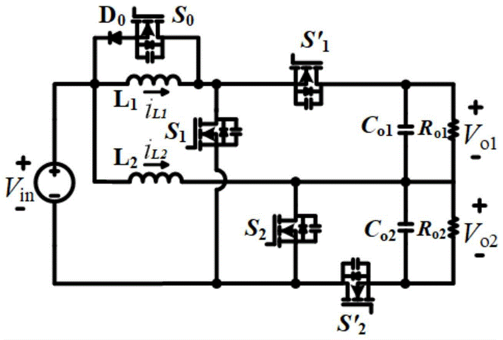
一种电压均衡三态双输出升压变换器,包括两个储能电感(L1、L2),两个主开关管(S1、S2),一个二极管(D0),一个辅助开关管(S0),两个副开关管(S'1、S'2),两个输出电容(Co1、Co2);A voltage balanced tri-state dual-output boost converter, including two energy storage inductors (L 1 , L 2 ), two main switches (S 1 , S 2 ), a diode (D 0 ), and an auxiliary switch Tube (S 0 ), two auxiliary switch tubes (S' 1 , S' 2 ), two output capacitors (C o1 , C o2 );
第一储能电感(L1)一侧与输入电源正极、二极管(D0)的负极相连,另一侧与第一主开关管(S1)的漏极、辅助开关管(S0)的漏极、第一副开关管(S'1)源极相连;二极管(D0)的正极与辅助开关管(S0)的源极相连;第一主开关管(S1)源极与输入电源负极相连;第一副开关管(S'1)漏极与第一输出电容(Co1)的一侧相连,第一输出电容(Co1)的另一侧与第二主开关管(S2)漏极相连;第二储能电感(L2)一侧与输入电源正极相连,另一侧与第二主开关管(S2)漏极、第二输出电容(Co2)的一侧相连;第二输出电容(Co2)的另一侧与第二副开关管(S'2)源极相连,第二主开关管(S2)源极与输入电源负极、第二副开关管(S'2)漏极相连。所述第一输出电容(Co1)和第一负载(Ro1)并联,第二输出电容(Co2)和第二负载(Ro2)并联。One side of the first energy storage inductor (L 1 ) is connected to the anode of the input power supply and the cathode of the diode (D 0 ), and the other side is connected to the drain of the first main switch (S 1 ) and the drain of the auxiliary switch (S 0 ). The drain is connected to the source of the first auxiliary switch (S' 1 ); the anode of the diode (D 0 ) is connected to the source of the auxiliary switch (S 0 ); the source of the first main switch (S 1 ) is connected to the input The negative pole of the power supply is connected; the drain of the first auxiliary switching tube (S' 1 ) is connected to one side of the first output capacitor (C o1 ), and the other side of the first output capacitor (C o1 ) is connected to the second main switching tube (S 2 ) The drain is connected; one side of the second energy storage inductor (L 2 ) is connected to the positive pole of the input power supply, and the other side is connected to the drain of the second main switch (S 2 ) and one side of the second output capacitor (C o2 ) connected; the other side of the second output capacitor (C o2 ) is connected to the source of the second auxiliary switch (S' 2 ), the source of the second main switch (S 2 ) is connected to the negative pole of the input power supply, and the second auxiliary switch (S' 2 ) connected to the drain. The first output capacitor (C o1 ) is connected in parallel with the first load (R o1 ), and the second output capacitor (C o2 ) is connected in parallel with the second load (R o2 ).
进一步地,所述第一储能电感(L1)和第二储能电感(L2)的感值相同,且应使每一相电路电流在对应主开关管导通前的死区时间内为负值,且足以使对应主开关管的体二极管导通。Further, the inductance values of the first energy storage inductance (L 1 ) and the second energy storage inductance (L 2 ) are the same, and each phase circuit current should be within the dead time before the corresponding main switch is turned on. is negative, and is sufficient to turn on the body diode of the corresponding main switch.
进一步地,两个输出电容(Co1、Co2)的电容值应足够大,使得两个输出电容电压视为恒定值。Further, the capacitance values of the two output capacitors (C o1 , C o2 ) should be large enough so that the voltages of the two output capacitors are regarded as constant values.
进一步地,第二主开关管(S2)的占空比应始终大于0.5。Further, the duty cycle of the second main switch (S 2 ) should always be greater than 0.5.
进一步地,所述第一储能电感(L1)、第一主开关管(S1)、第一副开关管(S'1)、第一输出电容(Co1)构成第一个单输出升压支路;所述第二储能电感(L2)、第二主开关管(S2)、第二副开关管(S'2)、第二输出电容(Co2)构成第二个单输出升压支路;所述辅助开关管(S0)和二极管(D0)构成辅助平衡支路。Further, the first energy storage inductor (L 1 ), the first main switch (S 1 ), the first auxiliary switch (S' 1 ), and the first output capacitor (C o1 ) form a first single output Step-up branch: the second energy storage inductor (L 2 ), the second main switch (S 2 ), the second auxiliary switch (S' 2 ), and the second output capacitor (C o2 ) constitute the second A single-output step-up branch; the auxiliary switching tube (S 0 ) and the diode (D 0 ) form an auxiliary balancing branch.
基于上述电压均衡三态双输出升压变换器的控制方法,在死区时间相同时,辅助开关管(S0)和二极管(D0)构成的辅助平衡支路不加入工作,第一主开关管(S1)和第一副开关管(S'1)互补导通,第二主开关管(S2)和第二副开关管(S'2)互补导通,且主开关管的占空比始终大于0.5,输出电压实现自均衡;在死区时间不同时,辅助开关管(S0)和二极管(D0)构成的辅助平衡支路加入工作,根据死区时间大小关系或输出电压大小关系,控制辅助开关管(S0)的导通时序,和仅需提前第一主开关管(S1)的关断时刻或推迟第一副开关管(S'1)的导通时刻,来构建第一相电感电流保持不变、第一相电感电压为0的工作模态,即电路的第三态。Based on the control method of the above-mentioned voltage balanced three-state dual-output boost converter, when the dead time is the same, the auxiliary balanced branch composed of the auxiliary switch tube (S 0 ) and the diode (D 0 ) does not work, and the first main switch The transistor (S 1 ) and the first auxiliary switch transistor (S' 1 ) conduct complementary conduction, the second main switch transistor (S 2 ) and the second auxiliary switch transistor (S' 2 ) conduct complementary conduction, and the occupation of the main switch transistor The duty ratio is always greater than 0.5, and the output voltage achieves self-balancing; when the dead time is different, the auxiliary switching tube (S 0 ) and the diode (D 0 ) are added to work, and the output voltage is adjusted according to the relationship between the dead time and the output voltage The size relationship, control the turn-on timing of the auxiliary switch (S 0 ), and only need to advance the turn-off time of the first main switch (S 1 ) or delay the turn-on time of the first auxiliary switch (S' 1 ), To construct the working mode in which the first-phase inductor current remains unchanged and the first-phase inductor voltage is 0, that is, the third state of the circuit.
进一步地,控制方法具体包括以下步骤:Further, the control method specifically includes the following steps:
步骤1.当输出电压不均衡时,首先确定死区时间大小关系,如果死区时间难以检测,则通过输出电压大小关系间接确定;
步骤2.如果第一相开关管的死区时间大于第二相开关管的死区时间,或第一输出电压大于第二输出电压,则在原本的控制时序基础上,提前关断第一主开关管(S1),且将第一主开关管(S1)的占空比减小D-0,第一主开关管(S1)关断的同时,辅助开关管(S0)导通且占空比为D-0,其余开关管控制时序不变;
如果第一相开关管的死区时间小于第二相开关管的死区时间,或第一输出电压小于第二输出电压,则在原本的控制时序基础上,第一副开关管(S'1)导通时刻延迟D-0Ts且关断时刻不变,此时第一副开关管(S'1)占空比需减小D-0,第一主开关管(S1)关断的同时,辅助开关管(S0)导通且占空比为D-0,其余开关管控制时序不变;其中,Ts为开关周期;If the dead time of the first phase switching tube is less than the dead time of the second phase switching tube, or the first output voltage is smaller than the second output voltage, based on the original control sequence, the first secondary switching tube (S' 1 ) the turn-on time is delayed by D -0 T s and the turn-off time remains unchanged. At this time, the duty cycle of the first secondary switch (S' 1 ) needs to be reduced by D -0 , and the first main switch (S 1 ) is turned off At the same time, the auxiliary switching tube (S 0 ) is turned on and the duty cycle is D -0 , and the control timing of the other switching tubes remains unchanged; where, T s is the switching period;
步骤3.步骤2得到的新控制时序对电路的开关管进行控制。
进一步地,步骤1中通过输出电压大小关系间接确定的具体规律为:若第一输出电压大于第二输出电压,则第一相开关管对应的死区时间大于第二相开关管的死区时间,若若第一输出电压小于第二输出电压,则第一相开关管对应的死区时间小于第二相开关管的死区时间。Further, in
进一步地,步骤2中第一相开关管的死区时间大于第二相开关管的死区时间,或第一输出电压大于第二输出电压时,辅助开关管(S0)的占空比为D-0,通过


本发明的机理为:当两个输出电压出现不均衡现象时,以第二输出电压为基准,基于两相开关管的死区时间大小关系或两个输出电压大小关系(即不平衡量),来改变S1或S'1的时序,并且通过引入辅助平衡支路,改变电感的工作状态来改变第一相输出电压,以达到消除电压不均衡的目的;其中,改变量的确定基于电感的伏秒平衡分析和电路的基尔霍夫电压定律分析所得。The mechanism of the present invention is: when the two output voltages are unbalanced, take the second output voltage as a reference, and based on the relationship between the dead time of the two-phase switching tubes or the relationship between the two output voltages (ie, the unbalanced amount), the Change the timing of S 1 or S' 1 , and change the first phase output voltage by introducing an auxiliary balancing branch and changing the working state of the inductor to achieve the purpose of eliminating voltage imbalance; the determination of the amount of change is based on the volts of the inductor The second equilibrium analysis and the Kirchhoff's voltage law analysis of the circuit are obtained.
综上所述,由于采用了上述技术方案,本发明的有益效果是:In summary, owing to adopting above-mentioned technical scheme, the beneficial effect of the present invention is:
本发明考虑各元件参数的不确定性,通过引入辅助的平衡支路,控制第一主开关管(S1)或第一副开关管(S'1)的导通时序,消除因死区时间不一致带来的电压不均衡问题,保证双极直流微网中变换器两个输出电压均衡。The present invention considers the uncertainty of the parameters of each component, and controls the conduction sequence of the first main switching tube (S 1 ) or the first secondary switching tube (S' 1 ) by introducing an auxiliary balancing branch to eliminate the dead time The problem of voltage imbalance caused by inconsistency ensures that the two output voltages of the converter in the bipolar DC microgrid are balanced.
附图说明Description of drawings
图1为电压均衡三态双输出升压变换器的电路结构图。Figure 1 is a circuit structure diagram of a voltage-balanced three-state dual-output boost converter.
图2为变换器在死区时间相同且额外平衡支路不工作时的关键理论波形。Figure 2 shows the key theoretical waveforms of the converter when the dead time is the same and the extra balancing branch is not working.
图3为变换器在死区时间不同且额外平衡支路不工作时的关键理论波形。Figure 3 shows the key theoretical waveforms of the converter with different dead times and the extra balancing branch not working.
图4为变换器在死区时间不同且额外平衡支路工作时的关键理论波形。Figure 4 shows the key theoretical waveforms of the converter with different dead times and additional balancing branch operation.
图5为变换器在死区时间不同且额外平衡支路工作时关键参数的仿真波形。Fig. 5 is the simulation waveform of key parameters when the converter has different dead time and an additional balanced branch works.
具体实施方式Detailed ways
为使本发明的目的、技术方案和优点更加清楚,下面结合实施方式和附图,对本发明作进一步地详细描述。In order to make the purpose, technical solution and advantages of the present invention clearer, the present invention will be further described in detail below in conjunction with the implementation methods and accompanying drawings.
一种电压均衡三态双输出升压变换器,其电路结构图如图1所示,该变换器拓扑包括:两个储能电感(L1、L2),两个主开关管(S1、S2),一个二极管(D0),一个辅助开关管(S0),两个副开关管(S'1、S'2),两个输出电容(Co1、Co2)。第一储能电感(L1)一侧与输入电源正极、二极管(D0)的负极相连,另一侧与第一主开关管(S1)的漏极、辅助开关管(S0)的漏极、第一副开关管(S'1)源极相连;二极管(D0)的正极与辅助开关管(S0)的源极相连;第一主开关管(S1)源极与输入电源负极相连;第一副开关管(S'1)漏极与第一输出电容(Co1)的一侧相连,第一输出电容(Co1)的另一侧与第二主开关管(S2)漏极相连;第二储能电感(L2)一侧与输入电源正极相连,另一侧与第二主开关管(S2)漏极、第二输出电容(Co2)的一侧相连;第二输出电容(Co2)的另一侧与第二副开关管(S'2)源极相连,第二主开关管(S2)源极与输入电源负极、第二副开关管(S'2)漏极相连。第一输出电容(Co1)和第一负载(Ro1)并联,第二输出电容(Co2)和第二负载(Ro2)并联。第一储能电感(L1)、第一主开关管(S1)、辅助开关管(S0)、二极管(D0)、第一副开关管(S'1)、第一输出电容(Co1)构成第一个单输出升压支路;第二储能电感(L2)、第二主开关管(S2)、第二副开关管(S'2)、第二输出电容(Co2)构成第二个单输出升压支路;所述辅助开关管(S0)和二极管(D0)构成辅助平衡支路。A voltage-balanced three-state dual-output boost converter, its circuit structure diagram is shown in Figure 1, the converter topology includes: two energy storage inductors (L 1 , L 2 ), two main switch tubes (S 1 , S 2 ), a diode (D 0 ), an auxiliary switch (S 0 ), two auxiliary switches (S' 1 , S' 2 ), and two output capacitors (C o1 , C o2 ). One side of the first energy storage inductor (L 1 ) is connected to the anode of the input power supply and the cathode of the diode (D 0 ), and the other side is connected to the drain of the first main switch (S 1 ) and the drain of the auxiliary switch (S 0 ). The drain is connected to the source of the first auxiliary switch (S' 1 ); the anode of the diode (D 0 ) is connected to the source of the auxiliary switch (S 0 ); the source of the first main switch (S 1 ) is connected to the input The negative pole of the power supply is connected; the drain of the first auxiliary switching tube (S' 1 ) is connected to one side of the first output capacitor (C o1 ), and the other side of the first output capacitor (C o1 ) is connected to the second main switching tube (S 2 ) The drain is connected; one side of the second energy storage inductor (L 2 ) is connected to the positive pole of the input power supply, and the other side is connected to the drain of the second main switch (S 2 ) and one side of the second output capacitor (C o2 ) connected; the other side of the second output capacitor (C o2 ) is connected to the source of the second auxiliary switch (S' 2 ), the source of the second main switch (S 2 ) is connected to the negative pole of the input power supply, and the second auxiliary switch (S' 2 ) connected to the drain. The first output capacitor (C o1 ) is connected in parallel with the first load (R o1 ), and the second output capacitor (C o2 ) is connected in parallel with the second load (R o2 ). The first energy storage inductor (L 1 ), the first main switch (S 1 ), the auxiliary switch (S 0 ), the diode (D 0 ), the first auxiliary switch (S' 1 ), the first output capacitor ( C o1 ) constitutes the first single-output boost branch; the second energy storage inductor (L 2 ), the second main switch (S 2 ), the second auxiliary switch (S' 2 ), the second output capacitor ( C o2 ) constitutes a second single-output boosting branch; the auxiliary switching tube (S 0 ) and diode (D 0 ) constitute an auxiliary balancing branch.
考虑两个输出负载为电阻负载(Ro1和Ro2)时,为了解决死区时间不同带来的电压不均衡问题,需要分别分析额外平衡支路不投入工作时和投入工作时的变换器工作情况。Considering that the two output loads are resistive loads (R o1 and R o2 ), in order to solve the voltage imbalance problem caused by different dead time, it is necessary to analyze the operation of the converter when the additional balancing branch is not in operation and when it is in operation Condition.
电路工作稳定时,假设两个输出电容(Co1、Co2)足够大使得两个输出电容电压(Vo1、Vo2)可视为恒定值,电容和电感不发生谐振,电感线性充电和放电。假设两个储能电感完全相同(L=L1=L2),两个输出电容完全相同(Co=Co1=Co2)。图1中电流从电感左侧流向右侧的方向规定为电流正方向。When the circuit works stably, assuming that the two output capacitors (C o1 , C o2 ) are large enough so that the two output capacitor voltages (V o1 , V o2 ) can be regarded as constant values, the capacitor and inductor do not resonate, and the inductor charges and discharges linearly . Assume that the two energy storage inductors are identical (L=L 1 =L 2 ), and the two output capacitors are identical (C o =C o1 =C o2 ). In Figure 1, the direction in which the current flows from the left side of the inductor to the right side is defined as the positive direction of the current.
参数定义及说明:Ts为开关周期;D1、D2分别是S1和S2的占空比,并且D2=D;Td1、Td2分别是S1和S2的死区时间;T_0是构建的三态的维持时间,即S0导通时长;Vo1、Vo2是电流仅有正值时的两个输出电压;V′o1,V′o2是引入三态后的两个输出电压;V″o1是死区时间不同且不引入均衡电路时的第一个输出的电压值;定义
首先分析额外平衡支路不投入工作时的变换器工作情况。Firstly, the working condition of the converter when the extra balanced branch is not put into operation is analyzed.
假设死区时间相同时(Td1=Td2),此时变换器工作情况和Kim S等人采用的变换器一致。电路有关关键参数波形如图2,此时两个主开关管(S1、S2)占空比一致(D1=D2=D),两个主开关管导通时序相差180°,且S1和S'1互补导通、S2和S'2互补导通。当电感电流(iL1、iL2)仅有正值时,对应的电感电压波形为虚线所示(VL1、VL2)。为了解决因负载不匹配时死区带来的输出电压不均衡问题,Kim S等人采用较小且合适的电感值,保证在全负载范围内的电感电流在对应开关管的死区时间内为负值。电感电流从仅有正值变成在死区时间内为负值的情况,对应于电感电压波形从图2中虚线(VL1、VL2)变为了实线(V'L1、V'L2)。因此基于前提假设,结合电感的伏秒平衡可知,图2中各阴影矩形面积相等(SO=SP=SM=SN),即电感的箝位变化相同,进而可以知道输出电压发生了相同改变。因此,此时无论负载是否匹配,两个输出电压始终是均衡的。与Kim S等人采取的方法一致,通过对电路进行稳态分析可以得到式(1):Assuming that the dead time is the same (T d1 =T d2 ), the working condition of the converter at this time is consistent with that of the converter adopted by Kim S et al. The relevant key parameter waveforms of the circuit are shown in Figure 2. At this time, the duty cycle of the two main switch tubes (S 1 , S 2 ) is the same (D 1 =D 2 =D), and the turn-on timing of the two main switch tubes differs by 180°, and S 1 and S' 1 are complementary to conduction, and S 2 and S' 2 are complementary to conduction. When the inductor current (i L1 , i L2 ) has only positive values, the corresponding inductor voltage waveform is shown by the dotted line (V L1 , V L2 ). In order to solve the problem of unbalanced output voltage caused by the dead zone when the load does not match, Kim S et al. adopted a small and appropriate inductance value to ensure that the inductor current within the full load range is negative value. The situation that the inductor current changes from only positive to negative in the dead time corresponds to the inductor voltage waveform changing from the dotted line (V L1 , V L2 ) in Figure 2 to the solid line (V' L1 , V' L2 ) . Therefore, based on the premise and the volt-second balance of the inductor, it can be seen that the areas of the shaded rectangles in Figure 2 are equal (S O = S P = S M = S N ), that is, the clamping changes of the inductance are the same, and it can be known that the output voltage has changed Same change. Therefore, no matter whether the load is matched or not, the two output voltages are always balanced. Consistent with the method adopted by Kim S et al., the formula (1) can be obtained by performing a steady-state analysis on the circuit:

然而考虑到各元器件参数的不确定性,各开关管死区时间可能并不相同(Td1≠Td2),此时电路的关键参数波形如图3。However, considering the uncertainty of the parameters of each component, the dead time of each switching tube may be different (T d1 ≠ T d2 ), and the key parameter waveform of the circuit at this time is shown in Figure 3.
当Td1>Td2时,电路的关键参数波形如图3(a)。由电感的箝位和伏秒平衡可知,图中阴影矩形面积关系为S'O=S'P>SM=SN。因此可以推出此时第一输出电压(V”o1)大于第二输出电压(V'o2)。类似于上一种情况,根据图3(a)中的开关管导通时序对电路进行稳态分析,可得式(2):When T d1 >T d2 , the key parameter waveform of the circuit is shown in Figure 3(a). From the clamping of the inductor and the volt-second balance, it can be seen that the area relationship of the shaded rectangle in the figure is S' O =S' P >S M =S N . Therefore, it can be deduced that the first output voltage (V" o1 ) is greater than the second output voltage (V' o2 ) at this time. Similar to the previous case, the circuit is stabilized according to the turn-on sequence of the switch tube in Figure 3(a) Analysis, available formula (2):

当Td1<Td2时,电路的关键参数波形如图3(b)。由电感的箝位和伏秒平衡可知,图中阴影矩形面积关系为S'O=S'P<SM=SN。所以此时第一输出电压(V”o1)小于第二输出电压关系为(V'o2)。根据图3(b)中的开关管导通时序对电路进行稳态分析也能得到式(2)。When T d1 <T d2 , the key parameter waveform of the circuit is shown in Figure 3(b). From the clamping of the inductor and the volt-second balance, it can be seen that the area relationship of the shaded rectangle in the figure is S' O =S' P <S M =S N . Therefore, the relationship between the first output voltage (V” o1 ) and the second output voltage at this time is (V' o2 ). The steady-state analysis of the circuit according to the turn-on sequence of the switch in Figure 3(b) can also obtain the formula (2 ).
综上可知,当开关管死区时间不同时,此时电路的两个输出电压不均衡。为了解决这个问题,本发明对电路加入额外的均衡电路,并且通过控制开关管的导通时序以达到电压均衡的目的。引入均衡电路后的电路关键参数波形如图4。It can be seen from the above that when the dead time of the switching tubes is different, the two output voltages of the circuit are unbalanced at this time. In order to solve this problem, the present invention adds an additional equalization circuit to the circuit, and achieves the purpose of voltage equalization by controlling the conduction sequence of the switch tube. The waveform of the key parameters of the circuit after the equalization circuit is introduced is shown in Figure 4.
当Td1>Td2时,为了实现电压均衡,以第二输出电压为基准来调整第一输出电压,需将第一主开关管S1提前D-0Ts关断,并在S1的关断时刻导通辅助开关管(S0),得到如图4(a)所示的控制时序。与图3(a)不同,此时第一主开关管S1的占空比变小成D1=D-D-0,引入了辅助开关管S0且导通时长为T-0,其余开关管的控制时序不变。在引入均衡电路之前,电感电流只有上升和下降两种状态,电感电压只有两种电平;引入均衡电路后,辅助开关管S0导通期间给电感电流和电压带来了新的状态(即第三态):在这段时间内电感电流保持不变,电感电压箝位到0。在Td1>Td2时,两个输出电压原本分别为V″o1和V'o2,这里为了让第一输出电压V'o1等于V'o2,需确定S0的导通时长T-0或占空比D-0。下面给出计算过程:When T d1 >T d2 , in order to achieve voltage balance and adjust the first output voltage based on the second output voltage, it is necessary to turn off the first main switch S 1 in advance of D -0 T s , and at S 1 The auxiliary switch tube (S 0 ) is turned on at the moment of turning off, and the control sequence shown in Fig. 4(a) is obtained. Different from Fig. 3(a), the duty cycle of the first main switching tube S 1 becomes smaller at this time to D 1 =DD -0 , the auxiliary switching tube S 0 is introduced and the conduction time is T -0 , and the other switching tubes The control timing remains unchanged. Before introducing the balanced circuit, the inductor current has only two states of rising and falling, and the inductor voltage has only two levels; after introducing the balanced circuit, the auxiliary switch S 0 brings a new state to the inductor current and voltage during the conduction period (ie Third state): During this time the inductor current remains constant and the inductor voltage is clamped to 0. When T d1 >T d2 , the two output voltages are originally V″ o1 and V' o2 respectively. Here, in order to make the first output voltage V' o1 equal to V' o2 , it is necessary to determine the conduction duration of S 0 T -0 or Duty cycle D -0 . The calculation process is given below:
首先由电感L1的伏秒平衡可以得到图4(a)中阴影矩形面积(SA、SB、SC)的关系,如式(3):Firstly, from the volt-second balance of the inductance L 1 , the relationship of the area of the shaded rectangle ( SA , S B , S C ) in Figure 4(a) can be obtained, as shown in formula (3):
SA+SB=SC (3);S A + S B = S C (3);
根据电感L1的箝位状态和各时间段长短,可以得到图4(a)中阴影矩形面积(SA、SB、SC)表达式如式(4):According to the clamping state of the inductor L 1 and the length of each time period, the expression of the area of the shaded rectangle (S A , S B , S C ) in Figure 4(a) can be obtained as formula (4):

然后(3)(4)两式联立可以得到式(5):Then formula (3) and (4) can be combined to get formula (5):
D_0Vin+V′o2(1-D-Dd1)=Vin (5);D _0 V in +V′ o2 (1-DD d1 )=V in (5);
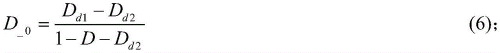
最终将式(5)分别与式(2)的两个方程式联立,整理后得到D-0的两种表达式,如式(6)和式(7):Finally, formula (5) is combined with the two formulas of formula (2), and two expressions of D -0 are obtained after finishing, such as formula (6) and formula (7):

当Td1>Td2时,由式(6)或式(7)可以确定控制量D-0:如果死区时间Td1、Td2可检测,可用式(6)确定D-0;如果死区时间Td1、Td2检测困难或检测不到,可以检测两个输出电压,当电压不均衡时,采用式(7)确定D-0。When T d1 >T d2 , the control value D -0 can be determined by formula (6) or formula (7): if the dead time T d1 and T d2 can be detected, D -0 can be determined by formula (6); It is difficult or impossible to detect the zone time T d1 and T d2 , and the two output voltages can be detected. When the voltages are unbalanced, formula (7) is used to determine D -0 .
当Td1<Td2时,仍然以第二输出电压为基准来调整第一输出电压,推迟第一副开关管(S'1)的导通时刻,且在第一主开关管(S1)的关断时刻导通辅助开关管(S0),得到如图4(b)所示的控制时序。与图3(b)中的不同,S'1不再与S1互补导通:图3中S1关断后,经过一个死区时间Td1后S'1导通,而在图4(b)中,S1关断后,经过Td1+T-0后S'1才导通,且S'1占空比相应减少了D-0;其中S1关断时辅助开关管(S0)随即导通且导通时长为T-0。同理,需确定S0的导通时长T-0或占空比D-0。下面给出计算过程:When T d1 <T d2 , the first output voltage is still adjusted based on the second output voltage, the turn-on moment of the first auxiliary switch (S' 1 ) is delayed, and the first main switch (S 1 ) The auxiliary switch tube (S 0 ) is turned on at the off time of , and the control sequence shown in Fig. 4(b) is obtained. Different from that in Figure 3(b), S' 1 is no longer complementary to S 1 and conducts: after S 1 is turned off in Figure 3, S' 1 conducts after a dead time T d1 , while in Figure 4 ( In b), after S 1 is turned off, S' 1 is turned on after T d1 + T -0 , and the duty cycle of S' 1 is correspondingly reduced by D -0 ; when S 1 is turned off, the auxiliary switch (S 0 ) is then turned on for a duration of T -0 . Similarly, the conduction duration T -0 or duty cycle D -0 of S 0 needs to be determined. The calculation process is given below:
首先由电感L1的伏秒平衡可以得到图4(b)中阴影矩形面积(SA、SB、SC)的关系,如式(8):Firstly, from the volt-second balance of the inductance L 1 , the relationship of the area of the shaded rectangle ( SA , S B , S C ) in Figure 4(b) can be obtained, as shown in formula (8):
SA+SC=SB (8);S A + S C = S B (8);
图4(b)中阴影矩形面积(SA、SB、SC)表达式如式(9):The expression of the shaded rectangle area (S A , S B , S C ) in Figure 4(b) is as formula (9):

然后(8)(9)两式联立可以得到式(10):Then formula (10) can be obtained by combining the two formulas (8) and (9):

同理,最终将式(10)分别与式(2)的两个方程式联立,整理后得到D-0的两种表达式,如式(11)和式(12):In the same way, formula (10) is finally combined with the two formulas of formula (2), and two expressions of D -0 are obtained after finishing, such as formula (11) and formula (12):


计算过程结束。当Td1<Td2时,由式(11)或式(12)可以确定控制量D-0:类似地,若死区时间Td1、Td2可检测,可用式(11)确定D-0;若死区时间Td1、Td2检测困难或检测不到,采用式(12)确定D-0。The calculation process ends. When T d1 < T d2 , the control quantity D -0 can be determined by formula (11) or formula (12): similarly, if the dead time T d1 and T d2 can be detected, D -0 can be determined by formula (11) ; If it is difficult or impossible to detect the dead time T d1 and T d2 , use formula (12) to determine D -0 .
综上所述,本发明提出的一种电压均衡三态双输出升压变换器及其控制方法可总结如下:采用如图1所示的三态双输出升压变换器,电感值取合适大小,以确保在全负载范围内且无论两个负载是否匹配时,电感电流在死区时间内存在负值;当两个主开关管死区时间一致时,采用如图2所示的开关管控制时序;当Td1>Td2时,对应有第一输出电压大于第二输出电压,此时提前第一主开关管(S1)的关断时刻,且在第一主开关管(S1)的关断时刻导通辅助开关管(S0),得到如图4(a)所示的开关管控制时序,并通过式(6)或式(7)确定控制量D-0;当Td1<Td2时,对应有第一输出电压小于第二输出电压,则推迟第一副开关管(S'1)的导通时刻,且在第一主开关管(S1)的关断时刻导通辅助开关管(S0),得到如图4(b)所示的开关管控制时序,并通过式(11)或式(12)确定控制量D-0。In summary, a voltage balanced three-state dual-output boost converter and its control method proposed by the present invention can be summarized as follows: the three-state dual-output boost converter shown in Figure 1 is adopted, and the inductance value is selected as appropriate , to ensure that in the full load range and regardless of whether the two loads match, the inductor current has a negative value in the dead time; when the dead time of the two main switching tubes is consistent, the switching tube control shown in Figure 2 is adopted Timing: when T d1 >T d2 , corresponding to the first output voltage is greater than the second output voltage, at this time the turn-off time of the first main switch (S 1 ) is advanced, and the first main switch (S 1 ) Turn on the auxiliary switch tube (S 0 ) at the off time of , to obtain the control sequence of the switch tube as shown in Figure 4(a), and determine the control value D -0 by formula (6) or formula (7); when T d1 <T d2 , corresponding to the fact that the first output voltage is lower than the second output voltage, the turn-on moment of the first auxiliary switch (S' 1 ) is delayed, and the turn-on moment of the first main switch (S 1 ) is turned on Through the auxiliary switching tube (S 0 ), the switching tube control sequence shown in Figure 4(b) is obtained, and the control value D -0 is determined by formula (11) or formula (12).
仿真分析结果:Simulation analysis results:
图5为实例的仿真波形,其仿真参数为:输入电压Vin=20V,两个负载电阻相等Ro1=Ro2=300Ω,输出电容Co1=Co2=300μF;开关频率为50kHz,Ts=300μs,主开关管占空比D=0.7,储能电感L1=L2=27μH。图5中各图的波形参数从上到下依次是电感L1的电流、电感L2的电流、电感L1的电压、电感L2的电压、第一输出电压和第二输出电压。Figure 5 is the simulation waveform of the example, and its simulation parameters are: input voltage V in =20V, two load resistances are equal R o1 =R o2 =300Ω, output capacitance C o1 =C o2 =300μF; switching frequency is 50kHz, T s =300μs, the duty ratio of the main switch tube D=0.7, the energy storage inductance L 1 =L 2 =27μH. The waveform parameters of each figure in FIG. 5 are, from top to bottom, the current of the inductor L1 , the current of the inductor L2 , the voltage of the inductor L1 , the voltage of the inductor L2 , the first output voltage and the second output voltage.
图5(a)是当Td1>Td2时且均衡电路不参加工作时的关键参数波形。此时主开关管S1的死区时间Td1=2μs,主开关管S2的死区时间Td2=1μs。从式2可知,理论上两个输出电压分别为100V和80V。从仿真图可以看出仿真与理论一致。为了实现电压均衡,首先根据此时的死区时间(或输出电压)的大小关系,因为此时Td1>Td2(或第一输出电压大于第二输出电压),所以由式(6)或式(7)得到控制量D-0=0.2。然后将第一主开关管S1提前D-0Ts关断,即占空比从0.7变成Dd1=0.5,S1关断时辅助开关管S0导通且占空比为D-0,其余开关管控制时序不变,得到如图4(a)的开关管控制时序。采用改变后的控制时序,仿真得到图5(b)所示的仿真波形,可以看出成功构建了三态,即电感电流不变和电感电压箝位为0的工作模态。从图5(b)可以看出两个输出电压均衡都为80V,与理论相符。Figure 5(a) is the key parameter waveform when T d1 >T d2 and the equalization circuit does not participate in the work. At this time, the dead time T d1 of the main switch S 1 =2 μs, and the dead time T d2 of the main switch S 2 =1 μs. It can be known from
图5(c)是当Td1<Td2时且均衡电路不参加工作时的关键参数波形。此时主开关管S1的死区时间Td1=1μs,主开关管S2的死区时间Td2=2μs。同理可知,理论上两个输出电压分别为80V和100V。从仿真图可以看出仿真与理论一致。同样为了实现输出电压均衡的目的,由Td1<Td2(或第一输出电压小于第二输出电压)可知需利用式(11)或式(12)得到控制量D-0=0.0625。然后第一副开关管S'1的导通时刻在原来的导通时刻上延迟D-0Ts=1.25μs,而且在第一主开关管关断时让辅助开关管S0导通且占空比为D-0,得到如图4(b)的开关管控制时序图。在新的控制时序下,仿真可以得到图5(d)所示的仿真波形,可知三态构建成功。从图5(d)可以看出两个输出电压均衡都为100V,与理论相符。Figure 5(c) is the key parameter waveform when T d1 <T d2 and the equalization circuit does not participate in the work. At this time, the dead time T d1 of the main switch S 1 =1 μs, and the dead time T d2 of the main switch S 2 =2 μs. Similarly, it can be seen that theoretically the two output voltages are 80V and 100V respectively. It can be seen from the simulation figure that the simulation is consistent with the theory. Also in order to achieve output voltage balance, from T d1 <T d2 (or the first output voltage is smaller than the second output voltage), it can be seen that the control variable D -0 =0.0625 needs to be obtained by using formula (11) or formula (12). Then the turn-on moment of the first auxiliary switch S'1 is delayed from the original turn-on moment by D -0 T s =1.25μs, and when the first main switch is turned off, the auxiliary switch S0 is turned on and takes up The duty ratio is D -0 , and the timing diagram of switching tube control is obtained as shown in Fig. 4(b). Under the new control sequence, the simulation can get the simulation waveform shown in Figure 5(d), which shows that the three-state construction is successful. It can be seen from Fig. 5(d) that the two output voltages are balanced to 100V, which is consistent with the theory.
综上,本发明提供了一种电压均衡三态双输出升压变换器及其控制方法。该方案考虑到参数不确定性带来的死区时间不一致问题,基于一种输入并联输出串联变换器,通过添加辅助平衡支路,创建新的电路模态(第三态),提出了一种电压均衡三态双输出升压变换器及其控制方法,给出了确定控制开关管的导通时序的方法,最终解决了死区时间不一致带来的电压不均衡问题。To sum up, the present invention provides a voltage-balanced three-state dual-output boost converter and a control method thereof. Considering the inconsistency of dead time caused by parameter uncertainty, this scheme is based on an input parallel output series converter, and creates a new circuit mode (third state) by adding an auxiliary balance branch. The voltage balanced tri-state dual-output boost converter and its control method provide a method for determining the conduction sequence of the control switch tube, and finally solve the problem of voltage imbalance caused by inconsistent dead time.
以上所述,仅为本发明的具体实施方式,本说明书中所公开的任一特征,除非特别叙述,均可被其他等效或具有类似目的的替代特征加以替换;所公开的所有特征、或所有方法或过程中的步骤,除了互相排斥的特征和/或步骤以外,均可以任何方式组合。The above is only a specific embodiment of the present invention. Any feature disclosed in this specification, unless specifically stated, can be replaced by other equivalent or alternative features with similar purposes; all the disclosed features, or All method or process steps may be combined in any way, except for mutually exclusive features and/or steps.
Claims (9)


Priority Applications (1)
| Application Number | Priority Date | Filing Date | Title |
|---|---|---|---|
| CN202110960830.9A CN113691132B (en) | 2021-08-20 | 2021-08-20 | Voltage balance three-state double-output boost converter and control method thereof |
Applications Claiming Priority (1)
| Application Number | Priority Date | Filing Date | Title |
|---|---|---|---|
| CN202110960830.9A CN113691132B (en) | 2021-08-20 | 2021-08-20 | Voltage balance three-state double-output boost converter and control method thereof |
Publications (2)
| Publication Number | Publication Date |
|---|---|
| CN113691132A CN113691132A (en) | 2021-11-23 |
| CN113691132B true CN113691132B (en) | 2023-03-14 |
Family
ID=78581175
Family Applications (1)
| Application Number | Title | Priority Date | Filing Date |
|---|---|---|---|
| CN202110960830.9A Expired - Fee Related CN113691132B (en) | 2021-08-20 | 2021-08-20 | Voltage balance three-state double-output boost converter and control method thereof |
Country Status (1)
| Country | Link |
|---|---|
| CN (1) | CN113691132B (en) |
Citations (4)
| Publication number | Priority date | Publication date | Assignee | Title |
|---|---|---|---|---|
| CN105553266A (en) * | 2016-01-22 | 2016-05-04 | 江苏大学 | Interleaving high-gain Boost conversion circuit and working method thereof |
| CN105978332A (en) * | 2016-05-13 | 2016-09-28 | 重庆大学 | IPOS four-level Boost converter and midpoint potential balance control thereof |
| CN111464028A (en) * | 2020-03-31 | 2020-07-28 | 天津大学 | Non-isolated Low Current Ripple High Voltage Gain Soft Switching DC-DC Converter |
| CN111969847A (en) * | 2020-08-12 | 2020-11-20 | 西安交通大学 | Staggered non-isolated switch capacitor network high-gain soft switch converter and control method thereof |
Family Cites Families (1)
| Publication number | Priority date | Publication date | Assignee | Title |
|---|---|---|---|---|
| US9240712B2 (en) * | 2012-12-13 | 2016-01-19 | Power Systems Technologies Ltd. | Controller including a common current-sense device for power switches of a power converter |
-
2021
- 2021-08-20 CN CN202110960830.9A patent/CN113691132B/en not_active Expired - Fee Related
Patent Citations (4)
| Publication number | Priority date | Publication date | Assignee | Title |
|---|---|---|---|---|
| CN105553266A (en) * | 2016-01-22 | 2016-05-04 | 江苏大学 | Interleaving high-gain Boost conversion circuit and working method thereof |
| CN105978332A (en) * | 2016-05-13 | 2016-09-28 | 重庆大学 | IPOS four-level Boost converter and midpoint potential balance control thereof |
| CN111464028A (en) * | 2020-03-31 | 2020-07-28 | 天津大学 | Non-isolated Low Current Ripple High Voltage Gain Soft Switching DC-DC Converter |
| CN111969847A (en) * | 2020-08-12 | 2020-11-20 | 西安交通大学 | Staggered non-isolated switch capacitor network high-gain soft switch converter and control method thereof |
Non-Patent Citations (1)
| Title |
|---|
| An Input-Parallel-Output-Series Multilevel Boost Converter With a Uniform Voltage-Balance Control Strategy;CHEN, Jianfei 等;《IEEE Journal of Emerging and Selected Topics in Power Electronics》;20190126;全文 * |
Also Published As
| Publication number | Publication date |
|---|---|
| CN113691132A (en) | 2021-11-23 |
Similar Documents
| Publication | Publication Date | Title |
|---|---|---|
| Aravind et al. | A transformerless non-isolated multi-port DC–DC converter for hybrid energy applications | |
| DE102014103450B4 (en) | Power converter circuit comprising at least one battery | |
| CN107231089B (en) | Bidirectional three-level H-bridge non-isolated DC-DC converter | |
| Marjani et al. | A new dual output DC-DC converter based on SEPIC and Cuk converters | |
| CN106300964B (en) | Independent charge and discharge sequential single-inductance double-output switch converters method for controlling frequency conversion and its device | |
| Vekslender et al. | Closed-loop design and time-optimal control for a series-capacitor buck converter | |
| Pisano et al. | Micro-inverter for solar power generation | |
| CN113691132B (en) | Voltage balance three-state double-output boost converter and control method thereof | |
| Hao et al. | A new interleaved three-level boost converter and neutral-point potential balancing | |
| Li et al. | Soft-switching single stage isolated AC-DC converter for single-phase high power PFC applications | |
| Tang et al. | Energy injection ZVS full bridge converter with extended soft-switching range | |
| CN213637477U (en) | Combined continuous conduction mode single-inductor double-output switch converter frequency conversion control device | |
| Ghavaminejad et al. | Integrated buck-zeta converter | |
| Hulea et al. | An Improved Bidirectional Hybrid Switched Inductor Converter | |
| Rufer | A five-level NPC photovoltaic inverter with an actively balanced capacitive voltage divider | |
| CN112039341A (en) | Driving method of symmetrical half-bridge LC series resonance sine power conversion circuit | |
| CN117060721A (en) | Parameter design method of multiphase staggered parallel three-level DC-DC converter | |
| Kumar et al. | Implementation of Bi-directional DC-DC converter for PV energy system | |
| Zhao et al. | High gain single stage buck-boost inverter | |
| RU124455U1 (en) | RESONANT SWITCH | |
| JP2024065936A (en) | Three-level bidirectional dc-dc converter | |
| CN113162409A (en) | High-gain dual-output boost converter with inherent voltage-sharing and current-sharing characteristics | |
| Huynh et al. | Stability analysis of grid-connected flyback converter for PV power applications | |
| CN112993967B (en) | A Model Prediction Method for DC Microgrid Group Bus Tie Converter Based on Pulse Width Modulation | |
| Wang et al. | A new dual-active soft-switching converter for an MTEM electromagnetic transmitter |
Legal Events
| Date | Code | Title | Description |
|---|---|---|---|
| PB01 | Publication | ||
| PB01 | Publication | ||
| SE01 | Entry into force of request for substantive examination | ||
| SE01 | Entry into force of request for substantive examination | ||
| GR01 | Patent grant | ||
| GR01 | Patent grant | ||
| CF01 | Termination of patent right due to non-payment of annual fee | ||
| CF01 | Termination of patent right due to non-payment of annual fee |
Granted publication date: 20230314 |