Modes for carrying out the invention
The following describes embodiments with reference to the drawings. Note that the embodiments can be implemented in a plurality of different ways, and a person of ordinary skill in the art can easily understand the fact that the modes and details thereof can be changed into various forms without departing from the spirit and scope of the present invention. Therefore, the present invention should not be construed as being limited to the contents described in the following embodiments.
In the drawings described in the present specification, the size, layer thickness, or region of each component may be exaggerated for clarity.
The terms "first", "second", "third", and the like used in the present specification and the like are added to avoid confusion of the constituent elements, and are not limited in number.
In this specification and the like, for convenience, positional relationships of constituent elements will be described with reference to the drawings using terms such as "upper" and "lower" indicating arrangement. Further, the positional relationship of the constituent elements is changed as appropriate in accordance with the direction in which each structure is described. Therefore, the words described in the present specification are not limited to the words described in the present specification, and may be replaced as appropriate.
In this specification and the like, when transistors having different polarities are used or when the direction of current flow during circuit operation is changed, the functions of the source and the drain included in the transistor may be interchanged. Thus, "source" and "drain" may be interchanged.
Note that in this specification and the like, the channel length direction of the transistor refers to one of directions parallel to a straight line connecting the source region and the drain region at the shortest distance. That is, the channel length direction corresponds to one of the directions of current flowing in the semiconductor layer when the transistor is in an on state. The channel width direction is a direction orthogonal to the channel length direction. Depending on the structure and shape of the transistor, the channel length direction and the channel width direction may not be limited to one direction.
In this specification and the like, "electrically connected" includes a case where connection is made by "an element having some kind of electrical action". Here, the "element having a certain electric function" is not particularly limited as long as it can transmit and receive an electric signal between connection targets. For example, "an element having a certain electric function" includes not only an electrode and a wiring but also a switching element such as a transistor, a resistance element, an inductor, a capacitor, other elements having various functions, and the like.
In addition, in this specification and the like, "film" and "layer" may be interchanged with each other. For example, the terms "conductive layer", "insulating layer", and the like may be replaced with "conductive film" and "insulating film".
In this specification and the like, "the top surface is substantially uniform in shape" means that at least a part of the contour of each layer in the laminate overlaps. For example, the case where part or all of the upper layer and the lower layer are processed by the same mask pattern is also referred to. However, strictly speaking, the outlines may not overlap and the end of the upper layer may be located inside the end of the lower layer or the end of the upper layer may be located outside the end of the lower layer, and these cases are also included in the case of "the top surface shape is substantially uniform".
In this specification and the like, unless otherwise specified, an off-state current refers to a drain current when a transistor is in an off state (also referred to as a non-conductive state or an interruption state). In the n-channel transistor, the off state refers to a voltage V between the gate and the source, unless otherwise specifiedgsBelow threshold voltage Vth(in p-channel type transistors VgsHigher than Vth) The state of (1).
In this specification and the like, a display panel which is one embodiment of a display device is a panel which can display (output) an image or the like on a display surface. Therefore, the display panel is one mode of the output device.
In the present specification and the like, a structure in which a connector such as an FPC (Flexible Printed Circuit) or a TCP (Tape Carrier Package) is mounted On a substrate of a display panel, or a structure in which an IC is directly mounted On a substrate by a COG (Chip On Glass) method or the like is referred to as a display panel module or a display module, or simply referred to as a display panel.
Note that in this specification and the like, a touch panel which is one embodiment of a display device has the following functions: a function of displaying an image on a display surface; and a function as a touch sensor for detecting contact, click, or approach of an object to be detected such as a finger or a stylus to the display surface. The touch panel is one way of input/output device.
The touch panel may be referred to as a display panel (or a display device) having a touch sensor or a display panel (or a display device) having a touch sensor function, for example. The touch panel may include a display panel and a touch sensor panel. Alternatively, the display panel may have a structure in which the display panel has a function of a touch sensor inside or on the surface thereof.
In this specification and the like, a structure in which a connector or an IC is mounted on a substrate of a touch panel is sometimes referred to as a touch panel module, a display module, or simply a touch panel or the like.
(embodiment mode 1)
In this embodiment, a semiconductor device according to one embodiment of the present invention will be described. As an example of a semiconductor device, a structure example of a transistor and a manufacturing method thereof will be described below.
One embodiment of the present invention is a semiconductor device including a semiconductor layer which forms a channel, a second insulating layer which serves as a gate insulating layer, and a conductive layer which serves as a gate electrode over a first insulating layer. The semiconductor layer preferably contains a metal oxide (hereinafter also referred to as an oxide semiconductor) exhibiting semiconductor characteristics.
The semiconductor device includes a metal oxide layer between the second insulating layer and the conductive layer. The metal oxide layer preferably has conductivity, in which case the metal oxide layer is used as a part of the gate electrode.
In a cross section in the channel length direction, an end portion (contour) of the second insulating layer is preferably located inside an end portion (contour) of the semiconductor layer. In addition, in a cross section in the channel length direction, an end portion (contour) of the conductive layer and the metal oxide layer is preferably located inside an end portion (contour) of the second insulating layer.
The semiconductor device according to one embodiment of the present invention further includes a third insulating layer. The third insulating layer is preferably provided in contact with the top surface of the first insulating layer, the top surface and the side surface of the semiconductor layer, the top surface and the side surface of the second insulating layer, the side surface of the metal oxide layer, and the top surface and the side surface of the conductive layer. The first insulating layer and the third insulating layer are preferably made of a material that suppresses diffusion of impurities. For example, nitride is preferably used for both the first insulating layer and the third insulating layer. Further, by providing a region where the first insulating layer is in contact with the third insulating layer, diffusion of impurities into the transistor can be suppressed, thereby obtaining a highly reliable transistor.
The semiconductor layer includes a first region where a channel is formed, a pair of second regions sandwiching the first region, and a pair of third regions sandwiching the first region and the second region and serving as a source region and a drain region. The first region is a region overlapping with the first insulating layer and the metal oxide layer. The second region is a region overlapping with the second insulating layer and not overlapping with the metal oxide layer. The third region is a region not overlapping with the second insulating layer. Further, the third region preferably has a portion which is in contact with the third insulating layer and whose resistance is lower than that of the first region. The second region preferably has a portion whose resistance is higher than that of the third region.
The second region is used as an LDD (Lightly Doped Drain) region. By having the second region, a drain electric field can be relaxed, and a highly reliable transistor can be obtained even when the transistor is driven at high voltage.
Hereinafter, a more specific example will be described with reference to the drawings.
< structural example 1>
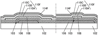
Fig. 1A is a top view of the transistor 100, fig. 1B is a sectional view taken along a chain line a1-a2 shown in fig. 1A, and fig. 1C is a sectional view taken along a chain line B1-B2 shown in fig. 1A. In fig. 1A, a part of the constituent elements (protective layer and the like) of the transistor 100 is omitted. The dotted line A1-A2 direction corresponds to the channel length direction, and the dotted line B1-B2 direction corresponds to the channel width direction. In the subsequent plan view of the transistor, a part of the components is omitted as in fig. 1A.
The transistor 100 is provided over a substrate 102, and includes an insulating layer 103, a semiconductor layer 108, an insulating layer 110, a metal oxide layer 114, a conductive layer 112, an insulating layer 116, an insulating layer 118, and the like. The island-shaped semiconductor layer 108 is provided over the insulating layer 103. The insulating layer 110 is provided so as to cover a part of the top surface of the insulating layer 103 and a part of the top surface of the semiconductor layer 108. A metal oxide layer 114 and a conductive layer 112 are sequentially provided over the insulating layer 110, and have a portion overlapping with the semiconductor layer 108. Fig. 2A is an enlarged view of a region P surrounded by a dashed-dotted line in fig. 1B.
The end portions of the conductive layer 112 and the metal oxide layer 114 are located inside the end portion of the insulating layer 110. In other words, the insulating layer 110 has a portion protruding outside the end portions of the conductive layer 112 and the metal oxide layer 114 at least over the semiconductor layer 108.
The semiconductor layer 108 includes a region 108C serving as a channel formation region, a pair of regions 10gL sandwiching the region 108C, and a pair of regions 108N outside the region. The region 108L is a region of the semiconductor layer 108 which overlaps with the insulating layer 110 and does not overlap with the conductive layer 112. In fig. 2A, the width of the region 108C in the channel length direction of the transistor 100 is denoted by L1, and the width of the region 108L is denoted by L2.
The region 108C is used as a channel formation region. Here, since the metal oxide layer 114 functions as a part of a gate electrode when it has conductivity, an electric field is applied to the region 108C through the insulating layer 110 functioning as a gate insulating layer to form a channel.
The region 108L functions as a buffer region for relaxing a drain electric field. Since the region 108L does not overlap with the conductive layer 112 and the metal oxide layer 114, a channel is hardly formed even when a gate voltage is applied to the conductive layer 112. The carrier concentration of the region 108L is preferably higher than that of the region 108C. Thereby, the region 108L can be used as an LDD region.
Region 108L can also be said to be: a region having a resistance approximately equal to or lower than that of region 108C; a region having a carrier concentration approximately equal to or higher than that of the first region; a region having an oxygen defect density approximately equal to or higher than that of the first region; a region having an impurity concentration substantially equal to or higher than that of the above-described region.
Region 108L can also be said to be: a region having a resistance approximately equal to or higher than that of the region 108N; a region having a carrier concentration approximately equal to or lower than that of the first region; a region having an oxygen defect density approximately equal to or lower than that of the first region; a region having an impurity concentration substantially equal to or lower than that of the above-described region.
As described above, by providing the region 108L used as an LDD region between the region 108C which is a channel formation region and the region 108N which is a source region or a drain region, a highly reliable transistor having both high drain withstand voltage and high on-state current can be realized.
The region 108N is used as a source region or a drain region having a lower resistance than other regions of the semiconductor layer 108. Alternatively, the region 108N may be said to be: a region having the highest carrier concentration compared with other regions of the semiconductor layer 108; a region having the highest oxygen defect density; or a region having the highest impurity concentration.
The lower the resistance of the region 108N is, the better, and for example, the sheet resistance value of the region 108N is preferably 1 Ω/□ or more and less than 1 × 10³Omega/□, more preferably 1 omega/□ or more and 8X 10²Omega/□ or less.
In addition, the higher the resistance of the region 108C in a state where no channel is formed, the better. For example, the sheet resistance value of the region 108C is 1 × 10⁹Omega/□ or more, preferably 5X 10⁹Omega/□ or more, more preferably 1X 10¹⁰Omega/□ or more.
The upper limit value of the region 108C in a state where no channel is formed is not particularly limited, since the higher the resistance is, the better. However, if the upper limit value is set, the sheet resistance value of the region 108C is, for example, 1 × 10⁹Omega/□ and 1 x 10¹²Omega/□ or less, preferably 5X 10⁹Omega/□ and 1 x 10¹²Omega/□ or less, more preferably 1X 10¹⁰Omega/mouth and 1 x 10¹²Omega/□ or less.
The sheet resistance of the region 108L may be, for example, 1 × 10³Omega/□ and 1 x 10⁹Omega/□ or less, preferably 1X 10³Omega/□ and 1 x 10⁸Omega/□ or less, more preferably 1X 10³Omega/□ and 1 x 10⁷Omega/□ or less. By setting the resistance value in the above range, a transistor with good electrical characteristics and high reliability can be realized. Further, the sheet resistance can be calculated from the resistance value. By providing the region 108L between the region 108N and the region 108C, the source-drain withstand voltage of the transistor 100 can be improved.
In addition, the resistance of the region 108C in a state where a channel is not formed may be 1 × 10 of the resistance of the region 108N6More than two times and 1X 10¹²Not more than twice, preferably 1X 10⁶More than two times and 1X 10¹¹Not more than twice, more preferably 1X 10⁶More than two times and 1X 10¹⁰The magnification is less.
The resistance of the region 108C in a state where no channel is formed may be 1 × 10 of the resistance of the region 108L0More than two times and 1X 10⁹Not more than twice, preferably 1X 101More than two times and 1X 10⁸Not more than twice, more preferably 1X 10²More than two times and 1X 10⁷The magnification is less.
The resistance of the region 108L may be 1 × 10 of the resistance of the region 108N0More than two times and 1X 10⁹Not more than twice, preferably 1X 101More than two times and 1X 10⁸Not more than twice, more preferably 1X 101More than two times and 1X 10⁷The magnification is less.
By providing the region 108L having the above resistance between the region 108N and the channel formation region, the source-drain withstand voltage of the transistor 100 can be improved.
The carrier concentration in the semiconductor layer 108 has a distribution in which the region 108C, the region 108L, and the region 108N increase in this order. By providing the region 108L between the region 108C and the region 108N, even if an impurity such as hydrogen diffuses from the region 108N in the manufacturing process, for example, the carrier concentration of the region 108C can be kept extremely low.
The lower the carrier concentration in the region 108C used as a channel formation region, the better, preferably 1 × 1018cm-3Hereinafter, more preferably 1 × 1017cm-3Hereinafter, more preferably 1 × 1016cm-3Hereinafter, more preferably 1 × 1013cm-3Hereinafter, more preferably 1 × 1012cm-3The following. Note that the lower limit of the carrier concentration of the region 108C is not particularly limited, and may be, for example, 1 × 10⁻⁹cm-3。
On the other hand, the carrier concentration in the region 108N may be, for example, 5 × 1018cm-3Above, preferably 1 × 1019cm-3Above, more preferably 5 × 1019cm-3The above. The upper limit of the carrier concentration in the region 108N is not particularly limited, and may be, for example, 5 × 1021cm-3Or 1X 1022cm-3And the like.
The carrier concentration in the region 108L may be a value between the region 108C and the region 108N. For example, it may be in the range of 1 × 1014cm-3Above and below 1X 1020cm-3Within the range of (1).
The carrier concentration in the region 108L may be uneven, and may have a gradient that decreases from the region 108N side toward the channel formation region side. For example, the gradient may be such that one or both of the hydrogen concentration and the oxygen vacancy concentration in the region 108L decreases from the region 108N side toward the channel formation region side.
The semiconductor layer 108 preferably comprises a metal oxide. The insulating layer 103 and the insulating layer 110 which are in contact with the channel formation region of the semiconductor layer 108 are preferably formed using an oxide film. For example, an oxide film such as a silicon oxide film, a silicon oxynitride film, or an aluminum oxide film can be used. Thus, oxygen can be desorbed from the insulating layer 103 or the insulating layer 110 by heat treatment or the like in the manufacturing process of the transistor 100 and supplied to the channel formation region of the semiconductor layer 108, thereby reducing oxygen vacancies in the semiconductor layer 108.
A portion of the end portion of the insulating layer 110 is located on the semiconductor layer 108. The insulating layer 110 includes a portion which overlaps the conductive layer 112 to be used as a gate insulating layer and a portion which does not overlap the conductive layer 112 and the metal oxide layer 114 (i.e., a portion which overlaps the region 108L).
The insulating layer 110 may have a stacked-layer structure of two or more layers. Fig. 1B, 1C, and 2A show an example in which the insulating layer 110 has a three-layer structure of an insulating layer 110a, an insulating layer 110B over the insulating layer 110a, and an insulating layer 110C over the insulating layer 110B. Further, since insulating films made of the same kind of material can be used for the insulating layer 110a, the insulating layer 110b, and the insulating layer 110c, the interface between the insulating layer 110a, the insulating layer 110b, and the insulating layer 110c may not be clearly confirmed. Therefore, in this embodiment, the interface between the insulating layer 110a, the insulating layer 110b, and the insulating layer 110c is illustrated by a dotted line.
The insulating layer 110a includes a region in contact with a channel formation region of the semiconductor layer 108. The insulating layer 110c includes a region in contact with the metal oxide layer 114. The insulating layer 110b is located between the insulating layer 110a and the insulating layer 110 c.
The insulating layer 110a, the insulating layer 110b, and the insulating layer 110c are preferably insulating films including oxide. In this case, the insulating layer 110a, the insulating layer 110b, and the insulating layer 110c are preferably formed continuously using the same film forming apparatus.
For example, as the insulating layer 110a, the insulating layer 110b, and the insulating layer 110c, one or more insulating layers including a silicon oxide film, a silicon oxynitride film, a silicon nitride oxide film, an aluminum oxide film, a hafnium oxide film, an yttrium oxide film, a zirconium oxide film, a gallium oxide film, a tantalum oxide film, a magnesium oxide film, a lanthanum oxide film, a cerium oxide film, and a neodymium oxide film can be used.
Further, the insulating layer 110 in contact with the semiconductor layer 108 preferably has a stacked-layer structure of an oxide insulating film, and more preferably has a region in which the oxygen content exceeds the stoichiometric composition. In other words, the insulating layer 110 has an insulating film capable of releasing oxygen. For example, oxygen can be supplied into the insulating layer 110 by forming the insulating layer 110 in an oxygen atmosphere, performing heat treatment, plasma treatment, or the like on the formed insulating layer 110 in an oxygen atmosphere, or forming an oxide film or the like on the insulating layer 110 in an oxygen atmosphere.
For example, the insulating layer 110a, the insulating layer 110b, and the insulating layer 110c can be formed by a sputtering method, a Chemical Vapor Deposition (CVD) method, a vacuum evaporation method, a Pulsed Laser Deposition (PLD) method, an Atomic Layer Deposition (ALD) method, or the like. Examples of the CVD method include a Plasma Enhanced Chemical Vapor Deposition (PECVD) method and a thermal CVD method.
In particular, the insulating layer 110a, the insulating layer 110b, and the insulating layer 110c are preferably formed by a plasma CVD method.
The insulating layer 110a is formed over the semiconductor layer 108, and is preferably formed as thin as possible without damaging the semiconductor layer 108. For example, the film can be formed under a condition that the film forming rate (also referred to as a film forming rate) is sufficiently low.
For example, when the insulating layer 110a is formed by a plasma CVD method, damage to the semiconductor layer 108 can be made extremely small by forming under a low power condition.
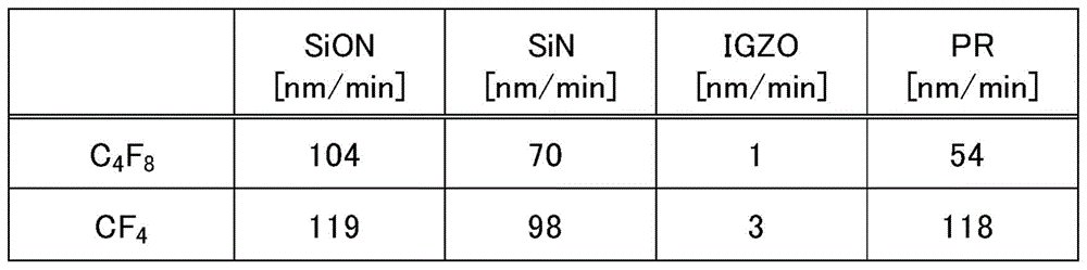
When a silicon oxynitride film is used as the insulating layer 110a, the insulating layer 110b, and the insulating layer 110c, a source gas containing a deposition gas containing silicon such as silane or disilane and an oxidation gas such as oxygen, ozone, nitrous oxide, or nitrogen dioxide can be used as a film formation gas for forming the silicon oxynitride film. In addition, a diluent gas such as argon, helium, or nitrogen may be contained in addition to the source gas.
For example, the film formation rate can be reduced by reducing the ratio of the flow rate of the deposition gas to the total flow rate of the film formation gas (hereinafter simply referred to as the flow rate ratio), and thus a dense film with fewer defects can be formed.
The insulating layer 110b is preferably a film formed under the condition that the film formation speed thereof is higher than that of the insulating layer 110 a. Thereby, productivity can be improved.
For example, when a condition that the flow rate of the deposition gas is increased as compared with the insulating layer 110a is adopted, the insulating layer 110b can be formed under a condition that the film formation speed is increased.
The insulating layer 110c is preferably an extremely dense film in which surface defects are reduced, and impurities contained in the atmosphere such as water are not easily attached. For example, the insulating layer 110a can be formed at a sufficiently low film formation rate.
Since the insulating layer 110c is formed over the insulating layer 110b, the semiconductor layer 108 is less affected when the insulating layer 110c is formed than when the insulating layer 110a is formed. Accordingly, the insulating layer 110c may be formed under a high power condition compared to the insulating layer 110 a. By reducing the flow ratio of the deposition gas and forming at higher power, a film that is dense and whose surface defects are reduced can be achieved.
In other words, a stacked layer formed under the condition that the insulating layer 110b, the insulating layer 110a, and the insulating layer 110c are sequentially formed at a high film formation rate to a low film formation rate may be used for the insulating layer 110. In the insulating layer 110, the etching rate under the same condition as that of the wet etching or the dry etching is, in order from high to low, the insulating layer 110b, the insulating layer 110a, and the insulating layer 110 c.
The thickness of the insulating layer 110b is preferably thicker than the insulating layers 110a and 110 c. By forming the insulating layer 110b having the highest film formation rate to be thick, the time required for the step of forming the insulating layer 110 can be shortened.
Here, since the boundary between the insulating layer 110a and the insulating layer 110b and the boundary between the insulating layer 110b and the insulating layer 110c may be unclear, these boundaries are shown by broken lines in fig. 1A and the like. Note that since the insulating layer 110a and the insulating layer 110b have different film densities, these boundaries may be observed in contrast in a Transmission Electron Microscope (TEM) image or the like of a cross section of the insulating layer 110. Similarly, a boundary between the insulating layer 110b and the insulating layer 110c may be observed.
When the conductive layer 112 and the metal oxide layer 114 are formed, the insulating layer 110 may have a reduced thickness in a region not overlapping with the conductive layer 112. Fig. 1B, 1C, and 2A show a structure in which the insulating layer 110C in a region not overlapping with the conductive layer 112 is removed and the insulating layer 110a and the insulating layer 110B remain. In addition, the thickness of the insulating layer 110b in a region not overlapping with the conductive layer 112 may be smaller than that of the insulating layer 110b in a region overlapping with the conductive layer 112.
By thinning the thickness of the insulating layer 110 in a region not overlapping with the conductive layer 112, hydrogen supplied from the insulating layer 116 can be increased to reduce the resistance of the region 108L. Further, by adjusting the thickness of the insulating layer 110 in a region not overlapping with the conductive layer 112, the amount of hydrogen supplied to the insulating layer 116 can be adjusted to control the resistance of the region 108L.
By reducing the thickness of the insulating layer 110 in a region not overlapping with the conductive layer 112, the step at the end of the insulating layer 110 is reduced, and the step coverage of a layer (for example, the insulating layer 116) formed over the insulating layer 110 is improved, whereby occurrence of defects such as disconnection or voids in the layer can be suppressed.
Fig. 2B shows a structure in which the insulating layer 110a, the insulating layer 110B, and the insulating layer 110c remain in a region not overlapping with the conductive layer 112. In addition, the insulating layer 110c in a region not overlapping with the conductive layer 112 may have a smaller thickness than the insulating layer 110c in a region overlapping with the conductive layer 112. As shown in fig. 2B, it is particularly preferable that the insulating layer 110c remains in a region not overlapping with the conductive layer 112. By adopting a structure in which the insulating layer 110c remains in a region not overlapping with the conductive layer 112, adsorption of water to the insulating layer 110 can be suppressed. The thickness of the insulating layer 110c in the region overlapping with the conductive layer 112 is 1nm or more and 50nm or less, preferably 2nm or more and 40nm or less, and more preferably 3nm or more and 30nm or less.
Fig. 2C shows an example in which the insulating layer 110a, the insulating layer 110b, and the insulating layer 110C remain in a region not overlapping with the conductive layer 112, in which the thickness of the insulating layer 110C in the region overlapping with the conductive layer 112 is substantially equal to the thickness of the insulating layer 110C in the region not overlapping with the conductive layer 112.
Further, the insulating layer 110 may have a two-layer structure of the insulating layer 110a and the insulating layer 110c over the insulating layer 110 a. Alternatively, the insulating layer 110 may have a single-layer structure. As the insulating layer 110, any one of the insulating layer 110a, the insulating layer 110b, and the insulating layer 110c described above can be appropriately selected according to the purpose.
The insulating layer 116 is provided so as to cover the top surface and the side surface of the conductive layer 112, the side surface of the metal oxide layer 114, the top surface and the side surface of the insulating layer 110, the top surface and the side surface of the semiconductor layer 108, and the top surface of the insulating layer 103. The insulating layer 118 is provided so as to cover the insulating layer 116. The insulating layer 116 and the insulating layer 118 function as protective layers and can suppress diffusion of impurity elements from the outside.
The insulating layer 116 has a function of suppressing diffusion of impurities from above the insulating layer 116 to the semiconductor layer 108. The insulating layer 116 also has a function of reducing the resistance of the semiconductor layer 108 in contact with the insulating layer 116 during film formation. An insulating layer 116 is disposed in contact with the top and side surfaces of the region 108N. The insulating layer 116 can be formed using an insulating film formed by supplying an impurity into the region 108N at the time of or after formation of the insulating layer 116. Alternatively, an insulating film which can generate oxygen vacancies in the region 108N by heating at the time of or after formation of the insulating layer 116 can be used.
The insulating layer 116 is preferably a film formed using a film-forming gas containing an impurity element such as hydrogen. For example, silane, ammonia, or the like can be used as the gas containing hydrogen. Further, by lowering the film formation temperature of the insulating layer 116, many impurity elements can be efficiently supplied to the semiconductor layer 108. The film formation temperature of the insulating layer 116 is, for example, preferably 200 ℃ to 500 ℃, more preferably 220 ℃ to 450 ℃, still more preferably 230 ℃ to 430 ℃, and yet more preferably 250 ℃ to 400 ℃.
When the insulating layer 116 is formed under reduced pressure while heating is performed, oxygen can be promoted to be desorbed from a region which becomes the region 108N in the semiconductor layer 108. When an impurity such as hydrogen is supplied to the semiconductor layer 108 in which many oxygen vacancies are formed, the carrier concentration in the region 108N is increased, and the resistance of the region 108N can be further effectively reduced.
As the insulating layer 116, for example, a nitride-containing insulating film such as silicon nitride, silicon nitride oxide, silicon oxynitride, aluminum nitride, or aluminum nitride oxide can be used as appropriate. In particular, since silicon nitride has barrier properties against hydrogen and oxygen, both diffusion of hydrogen from the outside to the semiconductor layer 108 and desorption of oxygen from the semiconductor layer 108 to the outside can be prevented, and thus a transistor with high reliability can be realized.
The insulating layer 116 may be an insulating film having a function of absorbing oxygen in the semiconductor layer 108 and generating oxygen vacancies. In particular, as the insulating layer 116, for example, a metal nitride such as aluminum nitride is preferably used.
In addition, in the case where the insulating layer 116 uses a metal nitride, it is preferable to use a nitride of aluminum, titanium, tantalum, tungsten, chromium, or ruthenium. For example, aluminum or titanium is particularly preferable. For example, with respect to an aluminum nitride film formed by a reactive sputtering method using aluminum as a sputtering target and a gas containing nitrogen as a film forming gas, a film having both extremely high insulation properties and extremely high barrier properties against hydrogen or oxygen can be formed by appropriately controlling the flow rate ratio of nitrogen with respect to the total flow rate of the film forming gas. Therefore, by providing an insulating film containing such a metal nitride in contact with the semiconductor layer 108, not only the resistance of the semiconductor layer 108 can be lowered, but also oxygen can be effectively prevented from being desorbed from the semiconductor layer 108 or hydrogen can be effectively prevented from diffusing into the semiconductor layer 108.
In the case of using aluminum nitride as the metal nitride, the thickness of the insulating layer containing the aluminum nitride is preferably 5nm or more. Even with such a thin film, the semiconductor layer can have both high barrier properties against hydrogen and oxygen and a function of reducing the resistance of the semiconductor layer. The thickness of the insulating layer is not particularly limited, but is preferably 500nm or less, more preferably 200nm or less, and still more preferably 50nm or less in view of productivity.
In the case where an aluminum nitride film is used as the insulating layer 116, a film whose composition formula satisfies A1Nx (x is a real number greater than 0 and 2 or less, and x is preferably a real number greater than 0.5 and 1.5 or less) is preferably used. Therefore, a film having high insulation and high thermal conductivity can be formed, and thus heat dissipation of heat generated when the transistor 100 is driven can be improved.
Alternatively, an aluminum titanium nitride film, a titanium nitride film, or the like can be used as the insulating layer 116.
Since such an insulating layer 116 is provided in contact with the region 108N, the insulating layer 116 absorbs oxygen in the region 108N, and oxygen vacancies can be generated in the region 108N. Further, when heat treatment is performed after such an insulating layer 116 is formed, more oxygen vacancies can be formed in the region 108N, and the resistance can be further reduced. In the case of using a film containing a metal oxide as the insulating layer 116, the insulating layer 116 absorbs oxygen in the semiconductor layer 108, whereby a layer including an oxide of a metal element (e.g., aluminum) contained in the insulating layer 116 is sometimes formed between the insulating layer 116 and the region 108N.
The region 108L is not in contact with the insulating layer 116 with the insulating layer 110 interposed therebetween, and therefore hydrogen supplied from the insulating layer 116 is less than that of the region 108N. Since the impurity concentration is also lower than that of the region 108N, the region 108L can have a higher resistance than that of the region 108N.
As described later, since the region 108L can be formed in self-alignment, a photomask for forming the region 108L is not required, and manufacturing cost can be reduced. Further, when the region 108L is formed in a self-aligned manner, relative misalignment between the region 108L and the conductive layer 112 does not occur, and thus the width of the region 108L in the semiconductor layer 108 can be substantially uniform.
A region 108L serving as a bias region to which a gate electric field is not applied (or which is less likely to be applied than a channel formation region) can be formed uniformly and stably between the channel formation region in the semiconductor layer 108 and the low-resistance region 108N. As a result, the source-drain withstand voltage of the transistor can be increased, and a transistor with high reliability can be realized.
The width L2 of the region 108L is preferably 100nm or more and 2 μm or less, more preferably 150nm or more and 1 μm or less, and further preferably 200nm or more and 1 μm or less. By providing the region 108L, concentration of an electric field in the vicinity of the drain can be alleviated, and therefore, deterioration of the transistor particularly in a state where the drain voltage is high can be suppressed. Further, particularly, by making the width L2 of the region 108L larger than the thickness of the insulating layer 110, concentration of an electric field in the vicinity of the drain can be effectively suppressed. On the other hand, if the width L2 exceeds 2 μm, the source-drain resistance increases, and the driving speed of the transistor may decrease. By setting the width L2 to the above range, a transistor and a semiconductor device with high reliability and high driving speed can be manufactured. The width L2 of the region 108L may be determined by the thickness of the semiconductor layer 108, the thickness of the insulating layer 110, and the magnitude of a voltage applied between the source and the drain when the transistor 100 is driven.
By providing the region 108L between the channel formation region and the low-resistance region 108N, the current density at the boundary between the channel formation region and the region 108N can be reduced, and heat generation at the boundary between the channel and the source or drain can be suppressed, whereby a transistor or a semiconductor device with high reliability can be manufactured.
The insulating layer 103 may have a stacked-layer structure. Fig. 1A to 1C show an example in which the insulating layer 103 has a stacked-layer structure in which an insulating layer 103a, an insulating layer 103b, an insulating layer 103C, and an insulating layer 103d are stacked from the substrate 102 side. The insulating layer 103a is in contact with the substrate 102. The insulating layer 103d is in contact with the semiconductor layer 108.
The insulating layer 103 preferably satisfies one of the following characteristics, more preferably satisfies all of the following characteristics: high withstand voltage, low stress, difficulty in releasing hydrogen and water, few defects, and suppression of diffusion of impurities contained in the substrate 102.
Among the four insulating films included in the insulating layer 103, insulating films containing nitrogen are preferably used for the insulating layer 103a, the insulating layer 103b, and the insulating layer 103c located on the substrate 102 side. On the other hand, an insulating film containing oxygen is preferably used for the insulating layer 103d in contact with the semiconductor layer 108. The four insulating films included in the insulating layer 103 are preferably formed continuously without being exposed to the atmosphere by a plasma CVD apparatus.
As each of the insulating layer 103a, the insulating layer 103b, and the insulating layer 103c, for example, a nitrogen-containing insulating film such as a silicon nitride film, a silicon oxynitride film, an aluminum nitride film, or a hafnium nitride film can be used. Note that the insulating layer 103d can be referred to as an insulating film which can be used for the insulating layer 110.
The insulating layers 103a and 103c are preferably dense films that prevent diffusion of impurities from below these films. Preferably, the insulating layer 103a can block impurities contained in the substrate 102, and the insulating layer 103c can block hydrogen and water contained in the insulating layer 103 b. Therefore, an insulating film formed at a lower film formation rate than that of the insulating layer 103b can be used for each of the insulating layers 103a and 103 c.
On the other hand, the insulating layer 103b is preferably formed using an insulating film which has low stress and is formed under conditions of high film formation speed. The insulating layer 103b is preferably formed thicker than the insulating layers 103a and 103 c.
For example, when a silicon nitride film formed by a plasma CVD method is used for the insulating layer 103a, the insulating layer 103b, and the insulating layer 103c, the film density of the insulating layer 103b is also lower than those of the other two insulating films. Therefore, in a transmission electron microscope image of a cross section of the insulating layer 103, these films are sometimes observed with a difference in contrast. Since the boundary between the insulating layer 103a and the insulating layer 103b and the boundary between the insulating layer 103b and the insulating layer 103C are sometimes unclear, these boundaries are shown by broken lines in fig. 1A to 1C and the like.
As the insulating layer 103d which is in contact with the semiconductor layer 108, a dense insulating film which hardly adsorbs impurities such as water on the surface thereof is preferably used. Further, it is preferable to use an insulating film having as few defects as possible and having reduced impurities such as water and hydrogen. For example, the insulating layer 103d may be formed using the same insulating film as the insulating layer 110c included in the insulating layer 110.
By using the insulating layer 103 having such a stacked-layer structure, the transistor can have extremely high reliability.
As shown in fig. 1B and 1C, the transistor 100 preferably has a region where the insulating layer 103C is in contact with the insulating layer 116. Fig. 3A is an enlarged view of a region Q surrounded by a dashed dotted line in fig. 1B, and fig. 3B is an enlarged view of a region R surrounded by a dashed dotted line in fig. 1C.
As shown in fig. 1B and 3A, the insulating layer 116 in a region not overlapping with the semiconductor layer 108 is in contact with the insulating layer 103c in the channel length direction. The end portion of the insulating layer 103d is substantially aligned with the end portion of the semiconductor layer 108.
As shown in fig. 3B, the insulating layer 116 in a region not overlapping with the insulating layer 110 is in contact with the insulating layer 103c in the channel width direction. The end portions of the insulating layer 103d are substantially aligned with the end portions of the insulating layer 110. For example, when the insulating layer 110 is formed, the insulating film serving as the insulating layer 103d in a region not overlapping with the insulating layer 110 is removed, whereby the end portion of the insulating layer 103d and the end portion of the insulating layer 110 can be aligned approximately.
By having a region where the insulating layer 103c is in contact with the insulating layer 116, diffusion of impurities from the outside to the transistor 100 can be suppressed. In particular, as the insulating layer 116 and the insulating layer 103c, an insulating film containing nitrogen is preferably used.
As shown in fig. 3C, the end portion of the insulating layer 103d may be substantially aligned with the end portion of the semiconductor layer 108. For example, when the semiconductor layer 108 is formed, the insulating film serving as the insulating layer 103d in a region not overlapping with the semiconductor layer 108 is removed, whereby the end portion of the insulating layer 103d and the end portion of the semiconductor layer 108 can be aligned approximately.
In the channel length direction, the thickness of the insulating layer 103c in a region not overlapping with the semiconductor layer 108 may be smaller than the thickness of the insulating layer 103c in a region overlapping with the semiconductor layer 108. Fig. 4A is an enlarged view of a region Q surrounded by a dashed-dotted line in fig. 1B. Fig. 4A shows the following example: the thickness of the insulating layer 103c in a region not overlapping with the semiconductor layer 108 is thinner than the thickness of the insulating layer 103c in a region overlapping with the semiconductor layer 108; in a region where the thickness of the insulating layer 103c is thin, the insulating layer 103c is in contact with the insulating layer 116.
In the channel width direction, the thickness of the insulating layer 103c in a region not overlapping with the insulating layer 110 may be smaller than the thickness of the insulating layer 103c in a region overlapping with the insulating layer 110. Fig. 4B and 4C are enlarged views of a region R surrounded by a dashed-dotted line in fig. 1C. Fig. 4B and 4C show the following examples: the thickness of the insulating layer 103c in a region not overlapping with the insulating layer 110 is thinner than the thickness of the insulating layer 103c in a region overlapping with the insulating layer 110; in a region where the thickness of the insulating layer 103c is thin, the insulating layer 103c is in contact with the insulating layer 116. In fig. 4B, the end of the insulating layer 103d is substantially aligned with the end of the insulating layer 110. In fig. 4C, the end portion of the insulating layer 103d is substantially aligned with the end portion of the semiconductor layer 108.
Fig. 4A, 4B, and 4C illustrate an example in which the insulating layer 103C is in contact with the insulating layer 116, but one embodiment of the present invention is not limited thereto, and the insulating layer 103B may be exposed so that the insulating layer 103B is in contact with the insulating layer 116. In addition, the insulating layer 103a may also be exposed so that the insulating layer 103a is in contact with the insulating layer 116.
The end of the insulating layer 110 and the end of the metal oxide layer 114 preferably have a tapered shape. With the above configuration, the coverage of the layer (for example, the insulating layer 116) formed over the insulating layer 110 and the metal oxide layer 114 is improved, and defects such as disconnection and voids can be suppressed from occurring in the layer.
A portion of the conductive layer 112 is used as a gate electrode. A portion of the insulating layer 110 is used as a gate insulating layer. The transistor 100 is a so-called top gate transistor in which a gate electrode is provided over a semiconductor layer 108.
As shown in fig. 1A and 1B, the transistor 100 may include a conductive layer 120a and a conductive layer 120B over the insulating layer 118. The conductive layers 120a and 120b function as source and drain electrodes. The conductive layer 120a and the conductive layer 120b are electrically connected to the region 108N through an opening 141a and an opening 141b provided in the insulating layer 118 and the insulating layer 116, respectively.
The semiconductor layer 108 preferably comprises a metal oxide.
For example, the semiconductor layer 108 preferably contains indium, an element M (M is one or more selected from gallium, aluminum, silicon, boron, yttrium, tin, copper, vanadium, beryllium, titanium, iron, nickel, germanium, zirconium, molybdenum, lanthanum, cerium, neodymium, hafnium, tantalum, tungsten, and magnesium), and zinc. In particular, M is preferably one or more selected from the group consisting of aluminum, gallium, yttrium, and tin.
In particular, as the semiconductor layer 108, an oxide containing indium, gallium, and zinc is preferably used.
The semiconductor layer 108 may have a stacked-layer structure in which layers having different compositions, layers having different crystallinity, or layers having different impurity concentrations are stacked.
The conductive layer 112 is preferably made of a low-resistance material. By using a low-resistance material for the conductive layer 112, parasitic resistance can be reduced, and a transistor can have a high on-state current, whereby a semiconductor device having a high on-state current can be realized. Further, in a large-sized display device or a high-definition display device, by reducing wiring resistance, signal delay can be suppressed and high-speed driving can be realized. For example, copper, silver, gold, aluminum, or the like can be used as the conductive layer 112. In particular, copper is preferably used because of its low electrical resistance and good mass productivity.
The conductive layer 112 may have a stacked-layer structure. When the conductive layer 112 has a stacked-layer structure, a second conductive layer is provided over and/or under the first conductive layer having low resistance. As the second conductive layer, a conductive material which is less easily oxidized (has oxidation resistance) than the first conductive layer is preferably used. In addition, as the second conductive layer, a material which suppresses diffusion of a component of the first conductive layer is preferably used. As the second conductive layer, for example, a metal oxide such as indium oxide, indium zinc oxide, Indium Tin Oxide (ITO), indium tin oxide containing silicon (ITSO), or zinc oxide, or a metal nitride such as titanium nitride, tantalum nitride, molybdenum nitride, or tungsten nitride is suitably used.
The metal oxide layer 114 located between the insulating layer 110 and the conductive layer 112 is used as a barrier film for preventing oxygen contained in the insulating layer 110 from diffusing to the conductive layer 112 side. Further, the metal oxide layer 114 is also used as a barrier film for preventing hydrogen or water contained in the conductive layer 112 from diffusing to the insulating layer 110 side. For example, a material that is less permeable to oxygen and hydrogen than at least the insulating layer 110 can be used for the metal oxide layer 114.
With the metal oxide layer 114, even in the case where a metal material such as aluminum or copper which is easily gettered with oxygen is used for the conductive layer 112, oxygen can be prevented from diffusing from the insulating layer 110 to the conductive layer 112. Further, in the case where the conductive layer 112 contains hydrogen, diffusion of hydrogen from the conductive layer 112 to the semiconductor layer 108 through the insulating layer 110 can also be prevented. As a result, the carrier concentration in the channel formation region of the semiconductor layer 108 can be extremely low.
As the metal oxide layer 114, an insulating material or a conductive material can be used. When the metal oxide layer 114 has an insulating property, the metal oxide layer 114 is used as a part of the gate insulating layer. On the other hand, when the metal oxide layer 114 has conductivity, the metal oxide layer 114 is used as a part of a gate electrode.
As the metal oxide layer 114, an insulating material having a higher dielectric constant than silicon oxide is preferably used. In particular, an aluminum oxide film, a hafnium aluminate film, or the like is preferably used because the driving voltage can be reduced.
As the metal oxide layer 114, a metal oxide can be used. For example, an oxide containing indium such as indium oxide, indium zinc oxide, Indium Tin Oxide (ITO), indium tin oxide containing silicon (ITSO), or the like can be used. It is preferable to use a conductive oxide containing indium because of its high conductivity. Further, ITSO is not easily crystallized when it contains silicon and has high flatness, and thus the adhesion of ITSO to a film formed thereon is improved. As the metal oxide layer 114, a metal oxide such as zinc oxide or zinc oxide containing gallium can be used. In addition, the metal oxide layer 114 may have a stacked-layer structure of the above materials.
As the metal oxide layer 114, an oxide material containing one or more elements which are the same as those of the semiconductor layer 108 is preferably used. In particular, an oxide semiconductor material applicable to the semiconductor layer 108 is preferably used. At this time, it is preferable that a device be shared by using a metal oxide film formed using the same sputtering target as the semiconductor layer 108 as the metal oxide layer 114.
In addition, when a metal oxide material containing indium and gallium is used for both the semiconductor layer 108 and the metal oxide layer 114, it is preferable that a material having a higher gallium composition (content ratio) than that of the semiconductor layer 108 be used for the metal oxide layer 114, since the barrier property against oxygen can be improved. At this time, by using a material whose indium composition is higher than that of the metal oxide layer 114 for the semiconductor layer 108, the field-effect mobility of the transistor 100 can be improved.
The metal oxide layer 114 is preferably formed using a sputtering apparatus. For example, when an oxide film is formed by a sputtering apparatus, oxygen can be added to the insulating layer 110 or the semiconductor layer 108 as appropriate by forming the oxide film in an atmosphere containing oxygen gas.
The semiconductor layer 108 has a channel formation region overlapping with the conductive layer 112 with the insulating layer 110 interposed therebetween. The semiconductor layer 108 has a pair of regions 108N sandwiching the channel formation region. The region 108N is a region of the semiconductor layer 108 which is not overlapped with the conductive layer 112 and the insulating layer 110 and is in contact with the insulating layer 116.
The region 108N can be a region having a lower resistance than the channel formation region, a region having a higher carrier concentration, a region having a higher oxygen defect density, a region having a higher impurity concentration, or a region exhibiting N-type.
The region 108N is a region containing an impurity element (first element). Examples of the impurity element include hydrogen, boron, carbon, nitrogen, fluorine, phosphorus, sulfur, arsenic, aluminum, magnesium, a rare gas, and the like. Typical examples of the rare gas include helium, neon, argon, krypton, and xenon. In particular, boron, phosphorus, magnesium or aluminum is preferably contained. Two or more of these elements may be contained.
Here, the concentration of the impurity of the region 108N preferably has a concentration gradient in which the concentration is higher as it approaches the insulating layer 116. Therefore, the total amount of the impurity elements in the region 108N can be further reduced as compared with the case where the entire region 108N has a uniform concentration, whereby the amount of impurities that are likely to diffuse to the channel formation region due to heating or the like in the manufacturing process can be kept at a small level. Thus, the resistance is lower as the region 108N is closer to the upper portion, and the contact resistance with the conductive layer 120a (or the conductive layer 120b) can be more effectively reduced.
As described later, the process of adding an impurity element to the region 108N can be performed using the insulating layer 110 as a mask. Thus, the region 108N can be formed in self-alignment.
The region 108N preferably has a concentration of impurities of 1 × 10¹⁹atoms/cm3Above and 1 × 10²³atoms/cm3Hereinafter, it is preferably 5 × 10¹⁹atoms/cm3Above and 5 × 10²²atoms/cm3Hereinafter, more preferably 1 × 10²⁰atoms/cm3Above and 1 × 10²²atoms/cm3The following region.
For example, the concentration of the impurities contained in the region 108N can be analyzed by Secondary Ion Mass Spectrometry (SIMS), X-ray Photoelectron Spectroscopy (XPS), or the like. In the case of using the XPS analysis technique, by combining the ion sputtering from the front surface side or the back surface side and the XPS analysis, the concentration distribution in the depth direction can be known.
The impurity element in the region 108N is preferably present in an oxidized state. For example, as the impurity element, an element which is easily oxidized, such as boron, phosphorus, magnesium, aluminum, and silicon, is preferably used. Since such an element that is easily oxidized can be stably present in a state of being oxidized by bonding with oxygen in the semiconductor layer 108, even if a high temperature (for example, 400 ℃ or higher, 600 ℃ or higher, 800 ℃ or higher) is applied in a subsequent step, desorption can be suppressed. Further, the impurity element abstracts oxygen in the semiconductor layer 108, thereby generating many oxygen vacancies (Vo) in the region 108N. A defect (hereinafter referred to as VoH) in which hydrogen in the film enters the oxygen vacancy (Vo) becomes a carrier supply source, and the region 108N becomes an extremely low resistance state.
Further, when a high temperature treatment is performed in a subsequent step, a large amount of oxygen may be supplied to the region 108N from the outside or a film in the vicinity of the region 108N, and the resistance may increase. Therefore, when the high-temperature treatment is performed, it is preferable to perform the treatment in a state where the semiconductor layer 108 is covered with the insulating layer 116 having high oxygen barrier properties.
The insulating layer 116 is provided so as to be in contact with the region 108N of the semiconductor layer 108.
The insulating layer 116 is used as a hydrogen supply source to the region 108N. For example, the insulating layer 116 is preferably a film that releases hydrogen by heating. By providing the insulating layer 116 so as to be in contact with the region 108N and performing heating after the insulating layer 116 is formed, hydrogen can be supplied to the region 108N to reduce resistance.
The insulating layer 116 is preferably a film formed using a gas containing hydrogen as a film formation gas used for film formation. This also allows hydrogen to be efficiently supplied to the region 108N even when the insulating layer 116 is formed.
As the insulating layer 116, an insulating film such as silicon nitride, silicon nitride oxide, silicon oxynitride, aluminum nitride, or aluminum nitride oxide can be used.
By adding the impurity element as described above, the region 108N is in a state including a plurality of oxygen vacancies. Therefore, the carrier concentration can be further increased due to oxygen supplied from the insulating layer 116 in addition to hydrogen in the semiconductor layer 108.
The insulating layer 118 is used as a protective layer for protecting the transistor 100. For the insulating layer 118, an inorganic insulating material such as oxide or nitride can be used. More specifically, an inorganic insulating material such as silicon nitride, silicon nitride oxide, silicon oxynitride, aluminum oxide, aluminum oxynitride, aluminum nitride, hafnium oxide, or hafnium aluminate can be used. In addition, the insulating layer 118 may also be used as a planarization layer. At this time, an organic resin material may be used as the insulating layer 118.
Note that an example in which the protective layer has a stacked-layer structure of the insulating layer 116 and the insulating layer 118 is shown here, but the insulating layer 118 may not be provided if not necessary. The insulating layer 118 may have a stacked-layer structure of two or more layers.
Here, the semiconductor layer 108 and oxygen vacancies that may be formed in the semiconductor layer 108 are explained.
The oxygen vacancy formed in the channel formation region of the semiconductor layer 108 causes a problem by having an influence on transistor characteristics. For example, when oxygen vacancies are formed in the semiconductor layer 108, hydrogen may enter the oxygen vacancies to become a carrier supply source. When a carrier supply source is generated in the channel formation region, the electrical characteristics of the transistor 100 vary, typically, the threshold voltage shifts. Therefore, in the channel forming region, the less oxygen vacancies are preferable.
In one embodiment of the present invention, the insulating film in the vicinity of the channel formation region of the semiconductor layer 108, specifically, the insulating layer 110 located above the channel formation region and the insulating layer 103 located below the channel formation region include oxide films. By transferring oxygen from the insulating layer 103 and the insulating layer 110 to the channel formation region by heating or the like in the manufacturing process, oxygen vacancies in the channel formation region can be reduced.
The semiconductor layer 108 preferably has a region In which the atomic number ratio of In to the element M is greater than 1. The higher the In content, the higher the field effect mobility of the transistor can be.
Here, In the metal oxide containing In, Ga, and Zn, the bonding force between In and oxygen is weaker than that between Ga and oxygen, and therefore, when the In content is high, oxygen vacancies are easily formed In the metal oxide film. In addition, the same tendency is also applied to the case where Ga is replaced with the metal element represented by the element M. When many oxygen vacancies exist in the metal oxide film, the electrical characteristics and reliability of the transistor are degraded.
However, In one embodiment of the present invention, a metal oxide material having a high In content can be used by supplying extremely large amounts of oxygen to the channel formation region of the semiconductor layer 108 including a metal oxide. Therefore, a transistor having extremely high field-effect mobility, stable electrical characteristics, and high reliability can be realized.
For example, a metal oxide In which the atomic number ratio of In to the element M is 1.5 or more, 2 or more, 3 or more, 3.5 or more, or 4 or more can be suitably used.
In particular, the ratio of the number of atoms of In, M, and Zn In the semiconductor layer 108 is preferably In, M, and Zn is 4: 2: 3 or In the vicinity thereof. Alternatively, the ratio of the number of atoms of In, M, and Zn In the semiconductor layer 108 is preferably In, M, and Zn In a ratio of 5: 1: 6 or In the vicinity thereof. In the composition of the semiconductor layer 108, the atomic numbers of In, M, and Zn In the semiconductor layer 108 may be substantially equal to each other. That is, the semiconductor layer 108 may include a material In which the atomic number of In, the element M, and Zn is In, M, and Zn In a ratio of 1: 1 or In the vicinity thereof.
For example, by using the transistor having high field effect mobility as a gate driver for generating a gate signal, a display device having a narrow frame width (also referred to as a narrow frame) can be provided. Further, by using the transistor having high field effect mobility as a source driver (particularly, a demultiplexer connected to an output terminal of a shift register included in the source driver), a display device having a small number of wirings connected to the display device can be provided.
Note that even if the semiconductor layer 108 includes a region In which the atomic number ratio of In to the element M is larger than 1, the field-effect mobility may be reduced when the crystallinity of the semiconductor layer 108 is high. The crystallinity of the semiconductor layer 108 can be analyzed by, for example, X-Ray Diffraction (XRD) or Transmission Electron Microscope (TEM).
Here, by reducing the impurity concentration and the defect state density (reducing oxygen vacancies) in the channel formation region of the semiconductor layer 108, the carrier concentration in the film can be reduced. A transistor in which this metal oxide film is used for a channel formation region of a semiconductor layer rarely has electrical characteristics of a negative threshold voltage (also referred to as normally-on characteristics). Further, a transistor using the metal oxide film has a characteristic that an off-state current is extremely small.
By using a metal oxide film with high crystallinity for the semiconductor layer 108, damage during processing of the semiconductor layer 108 or during formation of the insulating layer 110 can be suppressed, and thus a transistor with high reliability can be realized. On the other hand, by using a metal oxide film with low crystallinity for the semiconductor layer 108, conductivity can be improved, and thus a transistor with high field-effect mobility can be realized.
For example, a metal oxide film having a CAAC (c-axis aligned crystal) structure, a metal oxide film having an nc (nano crystal) structure, or a metal oxide film in which a CAAC structure and an nc structure are mixed is preferably used for the semiconductor layer 108.
The semiconductor layer 108 may have a stacked-layer structure of two or more layers.
For example, the semiconductor layer 108 in which two or more metal oxide films having different compositions are stacked may be used. For example, when an In-M-Zn oxide is used, it is preferable to use two or more films formed by a sputtering target In which In, M, and Zn are stacked at an atomic number ratio of 5: 1: 6, 4: 2: 3, 1: 1, 2: 1, 1: 3: 4, or 1: 3: 2.
Further, the semiconductor layer 108 in which two or more metal oxide films having different crystallinity from each other are stacked may be used. In this case, it is preferable to form the metal oxide film continuously under different film formation conditions using the same oxide target without exposure to the atmosphere.
At this time, a stacked structure of a metal oxide film having an nc structure and a metal oxide film having a CAAC structure can be used as the semiconductor layer 108. Alternatively, a stacked-layer structure of a metal oxide film having an nc structure and a metal oxide film having an nc structure may be employed. Further, the function or material structure of the metal oxide suitable for these metal oxide films can be described by CAC (Cloud-Aligned Composite) described later.
For example, the oxygen flow rate ratio at the time of forming the first metal oxide film formed first is set to be smaller than the oxygen flow rate ratio at the time of forming the second metal oxide film formed later. Alternatively, the conditions are adopted such that oxygen is not introduced during the formation of the first metal oxide film. Thereby, oxygen can be efficiently supplied at the time of film formation of the second metal oxide film. Further, the first metal oxide film may have lower crystallinity and higher conductivity than the second metal oxide film. On the other hand, by making the crystallinity of the second metal oxide film provided in the upper portion higher than that of the first metal oxide film, damage caused when the semiconductor layer 108 is processed or when the insulating layer 110 is formed can be suppressed.
More specifically, the oxygen flow rate ratio at the time of forming the first metal oxide film is 0% or more and less than 50%, preferably 0% or more and 30% or less, more preferably 0% or more and 20% or less, and typically 10%. The oxygen flow rate ratio at the time of forming the second metal oxide film is 50% or more and 100% or less, preferably 60% or more and 100% or less, more preferably 80% or more and 100% or less, further preferably 90% or more and 100% or less, and typically 100%. Further, the conditions such as pressure, temperature, and power at the time of forming the first metal oxide film and the second metal oxide film may be different from each other, but the conditions other than the oxygen flow rate ratio are preferably the same, because the time required for the film forming step can be shortened.
With the above configuration, the transistor 100 having excellent electric characteristics and high reliability can be realized.
Hereinafter, a structure example of a transistor having a partial structure different from that of the above-described structure example 1 will be described. Note that description of a part overlapping with the above configuration example 1 may be omitted below. In the drawings shown below, portions having the same functions as those of the above-described configuration example 1 are hatched with the same hatching, and no reference numeral is attached to the portions.
< structural example 2>
Fig. 5A is a top view of the transistor 100A, fig. 5B is a cross-sectional view in the channel length direction of the transistor 100A, and fig. 5C is a cross-sectional view in the channel width direction of the transistor 100A. Fig. 6A shows an enlarged view of a region P surrounded by a dashed-dotted line in fig. 5B. Fig. 6B shows an enlarged view of a region R surrounded by a dashed-dotted line in fig. 5C.
The transistor 100A differs from the transistor 100 mainly in that the end portion having the conductive layer 112 is located inside the end portion of the metal oxide layer 114. In addition, the insulating layer 116 is provided in contact with the top surface and the side surface of the metal oxide layer.
In the transistor 100A, an end portion of the conductive layer 112 is located inside an end portion of the metal oxide layer 114. In other words, the metal oxide layer 114 includes a portion protruding to the outside of the end portion of the conductive layer 112 at least on the insulating layer 110.
When the end portion of the conductive layer 112 is located inside the end portion of the metal oxide layer 114, the steps of the side surfaces of the conductive layer 112 and the metal oxide layer 114 are gentle, and the step coverage of a layer (for example, the insulating layer 116) formed over the conductive layer 112 and the metal oxide layer 114 is improved, whereby occurrence of defects such as disconnection or voids in the layer can be suppressed.
When the conductive layer 112 and the metal oxide layer 114 are formed, wet etching may be appropriately used. Further, by using a material having a lower etching rate than the conductive layer 112 in the metal oxide layer 114, the end portion of the conductive layer 112 can be located inside the end portion of the metal oxide layer 114. Further, the metal oxide layer 114 and the conductive layer 112 can be formed in the same step, thereby improving productivity.
The above is a description of configuration example 2.
< structural example 3>
Fig. 7A is a top view of the transistor 100B, fig. 7B is a cross-sectional view in the channel length direction of the transistor 100B, and fig. 7C is a cross-sectional view in the channel width direction of the transistor 100B. Fig. 8A shows an enlarged view of a region P surrounded by a dashed-dotted line in fig. 7B. Fig. 8B shows an enlarged view of a region Q surrounded by a dashed-dotted line in fig. 7B. Fig. 8C shows an enlarged view of a region R surrounded by a dashed-dotted line in fig. 7C.
The transistor 100B is different from the transistor 100A mainly in that the insulating layer 116 has a stacked-layer structure. The insulating layer 116 may have a stacked-layer structure of two or more layers. When the insulating layer 116 has a stacked-layer structure, the stacked-layer structure is not limited to a stacked-layer structure made of the same material, and may have a stacked-layer structure made of different materials.
Fig. 7B, 7C, 8A, 8B, and 8C show examples in which the insulating layer 116 has a two-layer structure of an insulating layer 116a and an insulating layer 116B over the insulating layer 116 a. As the insulating layer 116a and the insulating layer 116b, a material which can be used for the insulating layer 116 can be used. The insulating layer 116a and the insulating layer 116b may be formed using the same material or different materials. Since the insulating layers 116a and 116b may be formed using insulating films of the same material, the interface between the insulating layer 116a and the insulating layer 116b may not be clearly recognized. Therefore, in this embodiment, an interface between the insulating layer 116a and the insulating layer 116b is shown by a dotted line.
As shown in fig. 8A and 8B, the insulating layer 116 is in contact with the region 108N and is used as a hydrogen supply source to the region 108N. For example, the insulating layer 116 is preferably a film that releases hydrogen by heating.
The insulating layer 116 may be formed under an atmosphere containing hydrogen. For example, the insulating layer 116 is preferably formed by a plasma CVD method using a film forming gas containing hydrogen. For example, as the insulating layer 116, a silicon nitride film can be formed using a film formation gas containing a silane gas and an ammonia gas. Ammonia gas is used in addition to silane gas, whereby the hydrogen content of the insulating layer 116 can be increased. Further, when the insulating layer 116 is formed, hydrogen may also be supplied to the exposed portion of the semiconductor layer 108.
However, when the insulating layer 116 is formed in an atmosphere containing hydrogen, an exposed region of the semiconductor layer 108 may be reduced when the insulating layer 116 is formed. If the surface of the semiconductor layer 108 is reduced, the roughness of the surface of the semiconductor layer 108 increases, and defects such as disconnection or voids may occur in a layer (for example, the insulating layer 116) formed over the semiconductor layer 108.
Accordingly, the hydrogen content of the atmosphere for forming the insulating layer 116a on the semiconductor layer 108 side is preferably lower than the hydrogen content of the atmosphere for forming the insulating layer 116 b. For example, when the insulating layers 116a and 116b are formed, a mixed gas of silane, nitrogen, and ammonia may be used, in which the flow rate of ammonia for forming the insulating layer 116a is smaller than that for forming the insulating layer 116 b. In addition, when the insulating layer 116a is formed, a mixed gas of silane and nitrogen may be used, and when the insulating layer 116b is formed, a mixed gas of silane, nitrogen, and ammonia may be used. Further, the insulating layer 116a preferably has a region with a lower hydrogen concentration than the insulating layer 116 b. With such a structure, reduction of the surface of the semiconductor layer 108 can be suppressed.
For example, when a silicon nitride film formed by a plasma CVD method is used for the insulating layers 116a and 116b, a difference in contrast between the two, that is, a boundary between the two, may be observed from a Transmission Electron Microscope (TEM) image or the like on a cross section of the insulating layer 110 due to a difference in film density between the two. For example, the insulating layer 116a may have a region with a higher film density than the insulating layer 116 b. In TEM observation, a high film density gives a dark (dark) Transmission Electron (TE) image, and a low film density gives a light (bright) Transmission Electron (TE) image. Therefore, in the Transmitted Electron (TE) image, the insulating layer 116a may be a dark (dark) image compared to the insulating layer 116 b. Further, the insulating layer 116a may have a region with a lower hydrogen concentration than the insulating layer 116 b. The difference in hydrogen concentration between the insulating layer 116a and the insulating layer 116b can be evaluated by Secondary Ion Mass Spectrometry (SIMS), for example.
The insulating layer 116b is preferably made of a material which can block hydrogen, water, and oxygen. The barrier properties against hydrogen, water, and oxygen of the insulating layer 116b are preferably higher than those of the insulating layer 116 a. The insulating layer 116b provided over the insulating layer 116a can block hydrogen, water, and oxygen, and can suppress diffusion of hydrogen and water from the outside to the semiconductor layer 108 and release of oxygen from the semiconductor layer 108 to the outside, thereby realizing a highly reliable transistor.
Preferably, the insulating layer 116 in contact with the semiconductor layer 108 has few defects. For example, in the case where silicon nitride is used for the insulating layer 116, defects in the silicon nitride film are typically Kcenter or the like. K center is due to the dangling bonds of silicon and can be evaluated by Electron Spin Resonance (ESR).
When the hydrogen content of the atmosphere for forming the insulating layer 116a is less than that of the atmosphere for forming the insulating layer 116b, defects in the insulating layer 116a are sometimes more than those in the insulating layer 116 b. Therefore, in the case of the insulating layer 116 having only a single-layer structure of the insulating layer 116a, defects in the entire insulating layer 116 increase. Therefore, by providing the insulating layer 116 with a stacked-layer structure of the insulating layer 116a and the insulating layer 116b, defects in the entire insulating layer 116 can be reduced.
The thickness of the insulating layer 116b is preferably 0.5 to 30 times, more preferably 1 to 25 times, even more preferably 2 to 20 times, even more preferably 3 to 10 times, and even more preferably 4 to 5 times the thickness of the insulating layer 116 a. By providing the insulating layer 116 with a stacked-layer structure, the insulating layer 116 can block hydrogen, water, and oxygen and suppress reduction of the surface of the semiconductor layer 108 when the insulating layer 116 is formed, and the amount of defects in the insulating layer 116 can be reduced.
It is preferable that both the insulating layer 116a and the insulating layer 116b are formed continuously by using a plasma CVD apparatus so as not to be in contact with the atmosphere. By being formed continuously, impurities can be suppressed from adhering to the interface between the insulating layer 116a and the insulating layer 116 b. It is preferable that the insulating layer 116a, the insulating layer 116b, and the insulating layer 118 be formed continuously by using a plasma CVD apparatus so as not to be in contact with the atmosphere. By forming the insulating layers continuously, impurities can be prevented from adhering to the interface between the insulating layer 116a and the insulating layer 116b and the interface between the insulating layer 116b and the insulating layer 118.
The above is a description of configuration example 3.
< structural example 4>
Fig. 9A is a top view of the transistor 100C, fig. 9B is a cross-sectional view in the channel width direction of the transistor 100C, and fig. 9C is a cross-sectional view in the channel width direction of the transistor 100C.
The transistor 100C includes a conductive layer 106 between the substrate 102 and the insulating layer 103, and is different from the transistor 100 mainly in this point. The conductive layer 106 has a region overlapping with a channel formation region of the semiconductor layer 108, the metal oxide layer 114, and the conductive layer 112.
In the transistor 100C, the conductive layer 106 is used as a first gate electrode (also referred to as a bottom gate electrode), and the conductive layer 112 is used as a second gate electrode (also referred to as a top gate electrode). Further, a part of the insulating layer 103 is used as a first gate insulating layer, and a part of the insulating layer 110 is used as a second gate insulating layer.
A portion of the semiconductor layer 108 which overlaps with at least one of the conductive layer 112 and the conductive layer 106 is used as a channel formation region. Note that a portion of the semiconductor layer 108 which overlaps with the conductive layer 112 is sometimes referred to as a channel formation region for ease of description below, but actually, a channel may be formed in a portion which does not overlap with the conductive layer 112 but overlaps with the conductive layer 106 (a portion including the region 108N).
As shown in fig. 9A and 9C, the conductive layer 106 may be electrically connected to the conductive layer 112 through an opening 142 provided in the metal oxide layer 114, the insulating layer 110, and the insulating layer 103. This allows the conductive layer 106 and the conductive layer 112 to be supplied with the same potential.
The conductive layer 106 can be formed using the same material as the conductive layer 112, the conductive layer 120a, or the conductive layer 120 b. In particular, a material containing cu is preferably used for the conductive layer 106, and in this case, wiring resistance can be reduced. When a material containing a high-melting-point metal such as tungsten or molybdenum is used for the conductive layer 106, the material can be treated at a high temperature in a subsequent step.
As shown in fig. 9A and 9C, the conductive layer 112 and the conductive layer 106 preferably protrude outward from the end portion of the semiconductor layer 108 in the channel width direction. At this time, as shown in fig. 9C, the entire semiconductor layer 108 in the channel width direction is covered with the conductive layer 112 and the conductive layer 106 with the insulating layer 110 and the insulating layer 103 interposed therebetween.
By adopting the above structure, the semiconductor layer 108 can be electrically surrounded by an electric field generated by the pair of gate electrodes. In this case, it is particularly preferable to supply the same potential to the conductive layers 106 and 112. Thus, an electric field for inducing a channel can be effectively applied to the semiconductor layer 108, and therefore, the on-state current of the transistor 100C can be increased. Therefore, the transistor 100C can also be miniaturized.
Note that the conductive layer 112 and the conductive layer 106 may not be connected to each other. At this time, a constant potential may be supplied to one of the pair of gate electrodes, and a signal for driving the transistor 100C may be supplied to the other. In this case, the threshold voltage when the transistor 100C is driven by one gate electrode can be controlled by the potential supplied to the other gate electrode.
The insulating layer 103 may also have a stacked-layer structure. Fig. 9B and 9C show an example in which the insulating layer 103 has a structure in which an insulating layer 103a, an insulating layer 103B, an insulating layer 103C, and an insulating layer 103d are stacked in this order from the conductive layer 106 side. The insulating layer 103a is in contact with the conductive layer 106. The insulating layer 103a is preferably capable of blocking a metal element contained in the conductive layer 106. The insulating layers 103a, 103b, 103c, and 103d can be referred to above, and thus detailed description thereof is omitted.
For example, when a metal film or an alloy film which is less likely to diffuse into the insulating layer 103 is used as the conductive layer 106, three insulating films, i.e., the insulating layer 103b, the insulating layer 103c, and the insulating layer 103d, may be stacked without providing the insulating layer 103 a.
By using the insulating layer 103 having such a stacked-layer structure, the transistor can have extremely high reliability.
The above is a description of configuration example 4.
< production method example 1>
Hereinafter, a method for manufacturing a semiconductor device according to an embodiment of the present invention will be described with reference to the drawings. Here, the transistor 100C shown in the above configuration example will be described as an example.
Thin films (insulating films, semiconductor films, conductive films, and the like) constituting a semiconductor device can be formed by a sputtering method, a Chemical Vapor Deposition (CVD) method, a vacuum evaporation method, a Pulsed Laser Deposition (PLD) method, an Atomic Layer Deposition (ALD) method, or the like. Examples of the CVD method include a Plasma Enhanced Chemical Vapor Deposition (PECVD) method and a thermal CVD method. Further, as one of the methods of the thermal CVD method, a Metal Organic Chemical Vapor Deposition (MOCVD) method can be mentioned.
The thin films (insulating films, semiconductor films, conductive films, and the like) constituting the semiconductor device can be formed by a method such as a spin coating method, a dipping method, a spray coating method, an ink jet method, a dispenser method, a screen printing method, an offset printing method, a doctor blade (doctor knife) method, a slit coating method, a roll coating method, a curtain coating method, or a doctor blade coating method.
When a thin film constituting a semiconductor device is processed, the thin film can be processed by photolithography or the like. In addition to the above-described methods, the thin film may be processed by a nanoimprint method, a sandblasting method, a peeling method, or the like. The island-like thin film can be directly formed by a film formation method using a shadow mask such as a metal mask.
Photolithography typically has the following two methods. One is a method of forming a resist mask on a thin film to be processed, processing the thin film by etching or the like, and removing the resist mask. Another method is a method in which a photosensitive film is formed, and then the film is exposed and developed to be processed into a desired shape.
In the photolithography method, as the light used for exposure, for example, i-line (wavelength 365nm), g-line (wavelength 436nm), h-line (wavelength 405nm), or a mixture of these lights can be used. In addition, ultraviolet rays, KrF laser, ArF laser, or the like can be used. Further, exposure may be performed by an immersion exposure technique. As the light for exposure, Extreme ultraviolet light (EUV) or X-ray may also be used. In addition, an electron beam may be used instead of the light for exposure. When extreme ultraviolet light, X-rays, or electron beams are used, extremely fine processing can be performed, and therefore, such is preferable. Note that a photomask is not required when exposure is performed by scanning with a light beam such as an electron beam.
As a method for etching the thin film, a dry etching method, a wet etching method, a sandblasting method, or the like can be used.
Each of fig. 10A to 14B shows a cross section in each stage of the manufacturing process of the transistor 100C. In each figure, the left side of the central broken line shows a cross section in the channel length direction, and the right side of the central broken line shows a cross section in the channel width direction.
[ formation of conductive layer 106 ]
A conductive film is formed over the substrate 102, and is etched to obtain a conductive layer 106 which serves as a first gate electrode (see fig. 10A).
[ formation of insulating layer 103 ]
Next, an insulating layer 103 is formed so as to cover the substrate 102 and the conductive layer 106 (see fig. 10B). The insulating layer 103 can be formed by a PECVD method, an ALD method, a sputtering method, or the like.
Here, as the insulating layer 103, a stack of an insulating layer 103a, an insulating layer 103b, an insulating layer 103c, and an insulating layer 103d is formed. In particular, each insulating layer constituting the insulating layer 103 is preferably formed by a PECVD method.
The insulating layer 103a preferably has a function of blocking impurities. By providing the insulating layer 103a, diffusion of impurities from a lower layer of the insulating layer 103 to an upper layer of the insulating layer 103 can be suppressed. The insulating layer 103b preferably has a small stress and a high insulating withstand voltage. By providing the insulating layer 103b, the insulating layer 103 having a small stress and high insulation voltage resistance can be formed. It is preferable that the insulating layer 103c rarely releases impurities containing hydrogen and has a function of blocking impurities containing hydrogen. By providing the insulating layer 103c, diffusion of hydrogen into the channel formation region can be suppressed. It is preferable that the defect density of the insulating layer 103d is low and impurities containing hydrogen are rarely released.
A case where a silicon nitride film is used for the insulating layer 103a, the insulating layer 103b, and the insulating layer 103c, and a silicon oxynitride film is used for the insulating layer 103d will be described. The insulating layer 103a is formed by a plasma CVD method using a mixed gas of silane, nitrogen, and ammonia. Next, the insulating layer 103b having a small stress and high insulation and voltage resistance is formed using a mixed gas in which the ammonia flow rate is larger than that of the insulating layer 103 a. Next, an insulating layer 103c which has a small amount of released impurities including hydrogen and has a function of blocking impurities including hydrogen is formed using a mixed gas in which the ammonia flow rate is smaller than that of the insulating layer 103 b. Next, the insulating layer 103d having a low defect density and a small amount of released hydrogen-containing impurities is formed using a mixed gas of silane and dinitrogen monoxide, whereby the insulating layer 103 can be formed. Further, by switching the film formation conditions in the same process chamber, the insulating layer 103a, the insulating layer 103b, the insulating layer 103c, and the insulating layer 103d can be formed successively in vacuum, whereby the insulating layer 103 can be formed with high productivity.
Further, after the insulating layer 103c is formed, the surface of the insulating layer 103c is oxidized by plasma treatment in an atmosphere containing oxygen, whereby the insulating layer 103d can be formed over the insulating layer 103 c.
The density of the insulating layer 103b may be lower than that of the insulating layers 103a and 103 c. The difference in film density among the insulating layer 103a, the insulating layer 103b, and the insulating layer 103c can be evaluated by, for example, the density (luminance) of a TEM image. The insulating layer 103b may have a higher hydrogen concentration than the insulating layers 103a and 103 c. The difference in hydrogen concentration among the insulating layer 103a, the insulating layer 103b, and the insulating layer 103c can be evaluated by Secondary Ion Mass Spectrometry (SIMS), for example.
The treatment of supplying oxygen to the insulating layer 103 may be performed after the insulating layer 103 is formed. For example, plasma treatment, heat treatment, or the like may be performed under an oxygen atmosphere. Alternatively, oxygen may be supplied to the insulating layer 103 by a plasma ion doping method, an ion implantation method, or the like.
[ formation of the semiconductor layer 108 ]
Next, a metal oxide film 108f serving as the semiconductor layer 108 is formed over the insulating layer 103 (see fig. 10C).
The metal oxide film 108f is preferably formed by a sputtering method using a metal oxide target.
In forming the metal oxide film 108f, an oxygen gas and an inert gas (e.g., helium gas, argon gas, xenon gas, or the like) may be mixed. Note that the higher the proportion of oxygen gas (oxygen flow rate ratio) in the entire film forming gas at the time of forming the metal oxide film, the higher the crystallinity of the metal oxide film can be, and a transistor with high reliability can be realized. On the other hand, as the oxygen flow rate ratio is lower, the crystallinity of the metal oxide film is lower, and a transistor with high on-state current can be realized.
In the case where the semiconductor layer 108 has a stacked structure, it is preferable to form films continuously in the same film forming chamber using the same sputtering target because a good interface can be obtained. In particular, conditions such as pressure, temperature, and power can be varied when forming each metal oxide film, but the same conditions other than the oxygen flow rate ratio are preferable because the time required for the film forming step can be shortened. In addition, when metal oxide films having different compositions are stacked, it is preferable to form the films continuously without exposing them to the air.
Here, the film formation conditions of the metal oxide film 108f are preferably set so as to be a metal oxide film having a CAAC structure, a metal oxide film having an nc structure, or a metal oxide film in which a CAAC structure and an nc structure are mixed. Note that since the film formation conditions under which the metal oxide film to be formed has the CAAC structure and the film formation conditions under which the metal oxide film has the nc structure differ depending on the composition of the sputtering target to be used, the substrate temperature, the oxygen flow rate ratio, the pressure, the power, and the like can be appropriately set depending on the composition.
The substrate temperature may be set to room temperature or higher and 450 ℃ or lower, preferably room temperature or higher and 300 ℃ or lower, more preferably room temperature or higher and 200 ℃ or lower, and still more preferably room temperature or higher and 140 ℃ or lower as the film formation conditions of the metal oxide film 108 f. For example, in the case of using a large glass substrate or a resin substrate as the substrate 102, the substrate temperature is preferably equal to or higher than room temperature and lower than 140 ℃. Further, crystallinity can be reduced by forming a metal oxide film in a state where the substrate temperature is room temperature or heating is not performed.
It is preferable to perform a treatment for removing water, hydrogen, organic substances, and the like adhering to the surface of the insulating layer 103 or a treatment for supplying oxygen to the insulating layer 103 before the metal oxide film 108f is formed. For example, the heat treatment may be performed at a temperature of 70 ℃ or higher and 200 ℃ or lower in a reduced pressure atmosphere. Alternatively, the plasma treatment may be performed in an oxygen-containing atmosphere. Further, when the plasma treatment is performed under an atmosphere containing a nitrous oxide gas, organic matter on the surface of the insulating layer 103 can be appropriately removed. It is preferable that after such treatment, the metal oxide film be continuously formed in such a manner that the surface of the insulating layer 103 is not exposed to the atmosphere.
Next, the metal oxide film 108f is processed to form the island-shaped semiconductor layer 108 (see fig. 10D).
When the metal oxide film is processed, one or both of a wet etching method and a dry etching method may be used. At this time, a part of the insulating layer 103d which does not overlap with the semiconductor layer 108 may be removed by etching. By removing a part of the insulating layer 103d, the semiconductor layer 108 substantially conforms to the top surface of the insulating layer 103 d. Further, by removing a part of the insulating layer 103d, a part of the insulating layer 103c is exposed and the insulating layer 116 formed later is in contact with the insulating layer 103 c.
Further, after the metal oxide film is formed or after the metal oxide film is processed into the semiconductor layer 108, heat treatment may be performed to remove hydrogen or water in the metal oxide or the semiconductor layer 108. Typically, the temperature of the heat treatment may be set to 150 ℃ or higher and lower than the strain point of the substrate, 250 ℃ or higher and 450 ℃ or lower, or 300 ℃ or higher and 450 ℃ or lower. Further, the heat treatment may not be performed after the metal oxide film is formed or after the metal oxide film is processed into the semiconductor layer 108. Further, the heat treatment may be performed at any stage after the metal oxide film is formed. Further, the subsequent heat treatment or heat application step may be performed.
The heat treatment may be performed in an atmosphere containing a rare gas or nitrogen. Alternatively, the heating may be performed in an atmosphere containing oxygen after the heating in the atmosphere. As the nitrogen-containing atmosphere or oxygen-containing atmosphere, super Dry Air (CDA) may be used. The atmosphere of the heat treatment preferably does not contain hydrogen, water, or the like. Further, by using a high-purity gas having a dew point of-60 ℃ or lower, preferably-100 ℃ or lower, it is possible to prevent hydrogen, water, or the like from being mixed into the semiconductor layer 108 as much as possible. Further, an electric furnace, a Rapid Thermal Annealing (RTA) apparatus, or the like can be used for the heat treatment. By using the RTA apparatus, the heat treatment time can be shortened.
Further, the insulating film 110f is preferably formed immediately after the semiconductor layer 108 is formed. In a state where the surface of the semiconductor layer 108 is exposed, water may adhere to the surface of the semiconductor layer 108. When water adheres to the surface of the semiconductor layer 108, V may be formed by diffusion of hydrogen into the semiconductor layer 108 by subsequent heat treatment or the likeOH。VOSince H may be a generation source of carriers, it is preferable that the amount of water attached to the semiconductor layer 108 is small.
[ formation of insulating film 110f ]
Next, an insulating film 110f is formed so as to cover the insulating layer 103 and the semiconductor layer 108 (fig. 11A).
The insulating film 110f is a film which will be the insulating layer 110 later. As the insulating film 110f, for example, an oxide film such as a silicon oxide film or a silicon oxynitride film is preferably formed by using a plasma enhanced chemical vapor deposition apparatus (referred to as a PECVD apparatus or simply as a plasma CVD apparatus). Alternatively, the dielectric layer may be formed by a PECVD method using a microwave.
Here, an insulating film 110A, an insulating film 110B, and an insulating film 110C, which will be referred to as an insulating layer 110A, an insulating layer 110B, and an insulating layer 110C, respectively, are sequentially stacked. In particular, each insulating film constituting the insulating film 110f is preferably formed by a PECVD method.
A case where a silicon oxynitride film is used as the insulating film 110A, the insulating film 110B, and the insulating film 110C will be described. For example, the insulating film 110A is formed by a plasma CVD method using a mixed gas of silane and nitrous oxide. Next, the insulating film 110B is formed under the condition of using a mixed gas having a higher flow rate ratio of silane to the flow rate of nitrous oxide than the insulating film 110A and having a higher power. Next, the insulating film 110C is formed under a condition of using a mixed gas having a lower flow rate ratio of silane to the flow rate of nitrous oxide than the insulating film 110B and having a lower pressure, whereby the insulating film 110f can be formed. Further, by switching the film formation conditions in the same process chamber, the insulating film 110A, the insulating film 110B, and the insulating film 110C can be formed successively in vacuum, whereby the insulating film 110f can be formed with high productivity.
The heat treatment may be performed after the insulating film 110f is formed. By performing the heat treatment, impurities in the insulating film 110f and water on the surface of the insulating film 110f can be removed. The heat treatment may be performed at a temperature of 200 ℃ to 400 ℃ in an atmosphere containing one or more of nitrogen, oxygen, and a rare gas. Note that the insulating film 110f may not be subjected to heat treatment after formation. The heat treatment may be performed at any stage after the insulating film 110f is formed. Further, the subsequent heat treatment or heat application step may be performed.
It is preferable to perform plasma treatment on the surface of the semiconductor layer 108 before the formation of the insulating film 110 f. By this plasma treatment, impurities such as water attached to the surface of the semiconductor layer 108 can be reduced. Therefore, impurities at the interface between the semiconductor layer 108 and the insulating film 110f can be reduced, and thus a transistor with high reliability can be realized. In particular, when the surface of the semiconductor layer 108 is exposed to the atmosphere from the formation of the semiconductor layer 108 to the formation of the insulating film 110f, it is preferable to perform plasma treatment. The plasma treatment may be performed, for example, under an atmosphere containing oxygen, ozone, nitrogen, nitrous oxide, argon, or the like. It is preferable that the plasma treatment and the deposition of the insulating film 110f be performed continuously without exposure to the air.
Here, it is preferable to perform heat treatment after the insulating film 110f is formed. By the heat treatment, hydrogen or water contained in the insulating film 110f or attached to the surface can be removed. Further, defects in the insulating film 110f can be reduced.
The conditions of the heat treatment may be as described above.
The treatment of supplying oxygen to the insulating film 110f may be performed after the insulating film 110f is formed or after the heat treatment for removing the above-described hydrogen or water is performed. For example, plasma treatment, heat treatment, or the like may be performed in an oxygen-containing atmosphere. Alternatively, oxygen may be supplied to the insulating film 110f by a plasma ion doping method, an ion implantation method, or the like. In the plasma treatment, for example, a PECVD apparatus is suitably used. In the case of forming the insulating film 110f by a PECVD apparatus, it is preferable to perform plasma treatment continuously in vacuum after forming the insulating film 110 f. By continuously performing the formation of the insulating film 110f and the plasma treatment in vacuum, productivity can be improved.
In the case where the heat treatment is performed after the treatment of supplying oxygen to the insulating film 110f is performed, it is preferable to perform the heat treatment after forming a film (for example, a metal oxide film 114f) on the insulating film 110 f. When the heat treatment is performed in a state where the insulating film 110f is exposed, oxygen supplied to the insulating film 110f may be released to the outside of the insulating film 110 f. By performing the heat treatment after forming the film (e.g., the metal oxide film 114f) on the insulating film 110f, it is possible to suppress the oxygen supplied to the insulating film 110f from escaping out of the insulating film 110 f.
[ formation of Metal oxide film 114f ]
Next, a metal oxide film 114f is formed so as to cover the insulating film 110f (fig. 11B).
The metal oxide film 114f is a film which will be the metal oxide layer 114 later. In particular, the metal oxide film 114f is preferably formed by a sputtering method in an atmosphere containing oxygen, for example. Thereby, oxygen can be supplied to the insulating film 110f when the metal oxide film 114f is formed.
The above description can be applied to the case where the metal oxide film 114f is formed by a sputtering method using an oxide target containing a metal oxide, as in the case of the semiconductor layer 108.
For example, the metal oxide film 114f can be formed by a reactive sputtering method using oxygen as a film forming gas and a metal target. When aluminum is used as the metal target, an aluminum oxide film can be formed.
When the metal oxide film 114f is formed, the higher the ratio of the oxygen flow rate (oxygen flow rate ratio) in the total flow rate of the film formation gas introduced into the film formation chamber of the film formation apparatus or the oxygen partial pressure in the film formation chamber, the more the amount of oxygen supplied to the insulating film 110 can be increased. The oxygen flow rate ratio or the oxygen partial pressure is, for example, more than 0% and 100% or less, preferably 10% or more and 100% or less, more preferably 20% or more and 100% or less, further preferably 30% or more and 100% or less, and further preferably 40% or more and 100% or less. In particular, it is preferable to set the oxygen flow rate ratio to 100% so that the oxygen partial pressure is as close to 100% as possible.
In this manner, by forming the metal oxide film 114f by the sputtering method under the atmosphere containing oxygen, it is possible to prevent oxygen from being desorbed from the insulating film 110f while supplying oxygen to the insulating film 110f when forming the metal oxide film 114 f. As a result, an extremely large amount of oxygen can be confined in the insulating film 110 f. Further, by supplying a large amount of oxygen to the channel formation region of the semiconductor layer 108 by the subsequent heat treatment, oxygen vacancies in the channel formation region can be reduced, and thus a transistor with high reliability can be realized.
The substrate temperature may be set to room temperature or higher and 450 ℃ or lower, preferably room temperature or higher and 300 ℃ or lower, more preferably room temperature or higher and 200 ℃ or lower, and still more preferably room temperature or higher and 140 ℃ or lower as the film formation conditions of the metal oxide film 114 f. For example, when a large glass substrate or a resin substrate is used as the substrate 102, productivity is improved when the substrate temperature is equal to or higher than room temperature and lower than 140 ℃. When the temperature at which the metal oxide film 114f is formed is high, the crystallinity of the metal oxide film 114f is increased, and the etching rate may be lowered. When the film formation temperature of the metal oxide film 114f is low, the crystallinity of the metal oxide film 114f is low and the etching rate may be high. The film formation temperature of the metal oxide film 114f may be appropriately selected so that the etching rate is suitable for the etchant used for processing the metal oxide film 114 f.
Further, heat treatment may be performed after the metal oxide film 114f is formed to supply oxygen from the insulating film 110f to the semiconductor layer 108. The heat treatment may be performed at a temperature of 200 ℃ to 400 ℃ in an atmosphere containing one or more of nitrogen, oxygen, and a rare gas. Further, the heat treatment may not be performed after the metal oxide film 114f is formed. Further, the heat treatment is performed at an arbitrary stage after the metal oxide film 114f is formed. Further, the subsequent heat treatment or heat application step may be performed.
[ formation of conductive film 112f ]
Next, the opening 142 reaching the conductive layer 106 is formed by etching part of the metal oxide film 114f, the insulating film 110f, and the insulating layer 103. Thus, the conductive layer 112 formed later and the conductive layer 106 can be electrically connected through the opening 142.
Next, a conductive film 112f to be the conductive layer 112 is formed over the metal oxide film 114f (fig. 11C). The conductive film 112f is preferably formed by a sputtering method using a sputtering target of a metal or an alloy.
[ formation of insulating layer 110, Metal oxide layer 114, and conductive layer 112 ]
Next, a resist mask 115 is formed over the conductive film 112f (see fig. 12A). Then, the conductive film 112f and the metal oxide film 114f in the region not covered with the resist mask 115 are removed to form the conductive layer 112 and the metal oxide layer 114 (see fig. 12B).
When the conductive layer 112 and the metal oxide layer 114 are formed, wet etching may be appropriately used. As the wet etching method, for example, an etchant containing hydrogen peroxide can be used. For example, an etchant containing one or more of phosphoric acid, acetic acid, nitric acid, hydrochloric acid, and sulfuric acid may be used. In particular, when a material containing copper is used for the conductive layer 112, an etchant containing phosphoric acid, acetic acid, and nitric acid can be used as appropriate.
The conductive layer 112 and the metal oxide layer 114 are processed so that end portions thereof are positioned inside the contour of the resist mask 115. The conductive layer 112 and the metal oxide layer 114 are preferably formed by wet etching. By adjusting the etching time, the width L2 of the region 108L can be controlled.
In forming the conductive layer 112 and the metal oxide layer 114, the conductive film 112f and the metal oxide film 114f may be etched by an anisotropic etching method, and then the side surfaces of the conductive film 112f and the metal oxide film 114f may be etched by an isotropic etching method to recede the end surfaces (also referred to as side etching). Thus, the conductive layer 112 and the metal oxide layer 114 can be formed with their end portions positioned inside the insulating layer 110 in a plan view.
As shown in fig. 12B, when the conductive layer 112 and the metal oxide layer 114 are formed, the thickness of the insulating film 110f in a region not overlapping with the conductive layer 112 may be smaller than the thickness of the insulating film 110f in a region overlapping with the conductive layer 112.
In addition, when the conductive layer 112 and the metal oxide layer 114 are formed, etching may be performed at least twice using different etching conditions or methods. For example, the conductive film 112f may be etched first, and then the metal oxide film 114f may be etched under different etching conditions.
Next, the insulating film 110f is removed in a region not covered with the resist mask 115 to form the insulating layer 110 (see fig. 12C). In forming the insulating layer 110, either one or both of a wet etching method and a dry etching method can be used. Note that the insulating layer 110 may be formed in a state where the resist mask 115 is removed, but the film thickness of the conductive layer 112 may be suppressed from being thinned by not removing the resist mask 115. In addition, when the insulating layer 110 is formed, the insulating layer 103d in a region not covered with the resist mask 115 may be removed.
By adjusting the formation conditions of the insulating layer 110, the width L2 of the region 108L can be controlled. For example, by using a condition that the resist mask 115 is retracted when the insulating layer 110 is formed, the width of the resist mask 115 can be reduced. By reducing the width of the resist mask 115, the distance between the resist mask 115 and the end portion of the conductive layer 112 is reduced, and as a result, the width L2 of the region 108L can be reduced.
The resist mask 115 is removed after the insulating layer 110 is formed.
Here, washing for removing impurities may be performed. By performing the cleaning, impurities adhering to the exposed regions of the insulating layer 110 and the semiconductor layer 108 can be removed, and deterioration in electrical characteristics and reliability of the transistor can be suppressed. Examples of the impurities include components of an etching gas and an etchant that adhere when the insulating film 110f is etched, components of the conductive film 112f, and components of the metal oxide film 114 f.
As the washing method, wet washing with a washing liquid or the like, plasma treatment, or the like can be used. In addition, the washing may be appropriately combined. The wet cleaning may use a cleaning solution containing oxalic acid, phosphoric acid, ammonia water, hydrofluoric acid, or the like.
[ formation of insulating layer 116, region 108N (treatment for supplying Hydrogen) ]
Next, a process of supplying hydrogen to the exposed region of the semiconductor layer 108 is performed. Here, hydrogen is supplied by forming an insulating layer 116 containing hydrogen so as to be in contact with a region where the semiconductor layer 108 is exposed (fig. 13A).
The insulating layer 116 is preferably formed by a plasma CVD method using a film forming gas containing hydrogen. For example, a silicon nitride film is formed by using a film formation gas containing a silane gas and an ammonia gas. By using ammonia gas in addition to silane gas, a large amount of hydrogen can be contained in the film. In addition, hydrogen may be supplied to the exposed portion of the semiconductor layer 108 during film formation.
It is preferable that a part of hydrogen released from the insulating layer 116 be supplied to a part of the semiconductor layer 108 by performing heating treatment after the insulating layer 116 is formed. The heat treatment is preferably performed at a temperature of 150 ℃ or more and 450 ℃ or less, preferably 200 ℃ or more and 400 ℃ or less, in an atmosphere containing one or more of nitrogen, oxygen, and a rare gas.
By supplying hydrogen in the manner described above, a region 108N with very low resistance can be formed in the semiconductor layer 108.
By performing the heat treatment, oxygen can be supplied from the insulating layer 110 to the channel formation region of the semiconductor layer 108.
[ formation of insulating layer 118 ]
Next, an insulating layer 118 is formed over the insulating layer 116 (fig. 13B).
In the case where the insulating layer 118 is formed by using the plasma CVD method, when the film formation temperature is too high, impurities contained in the region 108N and the like may diffuse into the peripheral portion including the channel formation region of the semiconductor layer 108. As a result, the resistance of the channel formation region may decrease or the resistance of the region 108N may increase. The film formation temperature of the insulating layer 116 or the insulating layer 118 is, for example, preferably 150 ℃ or higher and 400 ℃ or lower, more preferably 180 ℃ or higher and 360 ℃ or lower, and further preferably 200 ℃ or higher and 250 ℃ or lower. By forming the insulating layer 118 at a low temperature, favorable electric characteristics can be obtained even for a transistor having a short channel length.
Further, heat treatment may be performed after the insulating layer 118 is formed.
[ formation of openings 141a and 141b ]
Next, after a mask is formed at a desired position of the insulating layer 118 by photolithography, the insulating layer 118 and the insulating layer 116 are partially etched, thereby forming an opening 141a and an opening 141b which reach the region 108N.
[ formation of conductive layers 120a and 120b ]
Next, a conductive film is formed over the insulating layer 118 so as to cover the openings 141a and 141b, and the conductive film is processed into a desired shape, thereby forming a conductive layer 120a and a conductive layer 120b (fig. 13C).
Through the above steps, the transistor 100C can be manufactured.
< production method example 2>
An example of the structure in which the end portion of the conductive layer 112 is located inside the end portion of the metal oxide layer 114 in the transistor 100A as an example of the structure will be described below.
Steps up to forming the resist mask 115 over the conductive film 112f are the same as in < manufacturing method example 1> described above (see fig. 12A).
[ formation of insulating layer 110, Metal oxide layer 114, and conductive layer 112 ]
Next, the conductive film 112f and the metal oxide film 114f in the region not covered with the resist mask 115 are removed to form a conductive layer 112 and a metal oxide layer 114 (see fig. 14A).
When the conductive layer 112 and the metal oxide layer 114 are formed, wet etching may be appropriately used. The conductive layer 112 and the metal oxide layer 114 are processed so that end portions thereof are positioned inside the contour of the resist mask 115. By adjusting the etching time, the width L2 of the region 108L can be controlled.
In forming the conductive layer 112 and the metal oxide layer 114, the conductive film 112f and the metal oxide film 114f may be etched by an anisotropic etching method, and then the side surfaces of the conductive film 112f and the metal oxide film 114f may be etched by an isotropic etching method to recede the end surfaces.
As shown in fig. 14A, when the conductive layer 112 and the metal oxide layer 114 are formed, the thickness of the insulating film 110f in a region not overlapping with the metal oxide layer 114 may be smaller than the thickness of the insulating film 110f in a region overlapping with the metal oxide layer 114.
When the conductive layer 112 and the metal oxide layer 114 are formed, an end portion of the conductive layer 112 may be recessed from an end portion of the metal oxide layer 114, and the thickness of the metal oxide layer 114 in a region not overlapping with the conductive layer 112 may be smaller than the thickness of the metal oxide layer 114 in a region overlapping with the conductive layer 112.
Next, the insulating film 110f is removed in a region not covered with the resist mask 115 to form the insulating layer 110 (see fig. 14B). In forming the insulating layer 110, either one or both of a wet etching method and a dry etching method can be used. Note that the insulating layer 110 may be formed in a state where the resist mask 115 is removed, but the film thickness of the conductive layer 112 may be suppressed from being thinned by not removing the resist mask 115.
After the insulating layer 110 is formed, the resist mask 115 is removed.
Hereinafter, the steps after the insulating layer 116 is formed may be referred to as the description of < manufacturing method example 1>, and thus detailed description thereof is omitted.
< Components of semiconductor device >
Next, the components included in the semiconductor device of the present embodiment will be described in detail.
[ substrate ]
Although the material and the like of the substrate 102 are not particularly limited, it is at least required to have heat resistance capable of withstanding subsequent heat treatment. For example, a single crystal semiconductor substrate or a polycrystalline semiconductor substrate made of silicon or silicon carbide, a compound semiconductor substrate such as silicon germanium, an SOI substrate, a glass substrate, a ceramic substrate, a quartz substrate, a sapphire substrate, or the like can be used as the substrate 102. Further, a substrate in which a semiconductor element is provided over the above substrate may be used as the substrate 102.
In addition, as the substrate 102, a flexible substrate may be used, and the transistor 100 and the like may be formed directly over the flexible substrate. Alternatively, a peeling layer may be provided between the substrate 102 and the transistor 100 or the like. The peeling layer may be used when a part or all of a semiconductor device is manufactured over the peeling layer and then separated from the substrate 102 and transferred to another substrate. In this case, the transistor 100 or the like may be provided over a substrate with low heat resistance or a flexible substrate.
[ insulating layer 103]
The insulating layer 103 can be formed by a sputtering method, a CVD method, an evaporation method, a Pulsed Laser Deposition (PLD) method, or the like as appropriate. Further, the insulating layer 103 may be formed using a single layer or a stacked layer of an oxide insulating film or a nitride insulating film, for example. Note that in order to improve interface characteristics between the insulating layer 103 and the semiconductor layer 108, at least a region in contact with the semiconductor layer 108 in the insulating layer 103 is preferably formed using an oxide insulating film. Further, a film which releases oxygen by heat is preferably used for the insulating layer 103.
The insulating layer 103 can be formed using, for example, silicon oxide, silicon oxynitride, silicon nitride oxide, silicon nitride, aluminum oxide, hafnium oxide, gallium oxide, Ga — Zn oxide, or the like, and can be formed in a stacked layer or a single layer.
When a film other than an oxide film such as a silicon nitride film is used on the side of the insulating layer 103 in contact with the semiconductor layer 108, a surface in contact with the semiconductor layer 108 is preferably subjected to pretreatment such as oxygen plasma treatment to oxidize the surface or the vicinity of the surface.
[ conductive film ]
The conductive layer 106, the conductive layer 120a functioning as a source electrode, and the conductive layer 120b functioning as a drain electrode can be formed using a metal element selected from chromium, copper, aluminum, gold, silver, zinc, molybdenum, tantalum, titanium, tungsten, manganese, nickel, iron, and cobalt, an alloy containing the metal element, an alloy containing a combination of the metal elements, or the like.
In addition, as the conductive layer 106, the conductive layer 120a, and the conductive layer 120b, an oxide conductor such as an In — Sn oxide, an In — W — Zn oxide, an In — Ti — Sn oxide, an In — Zn oxide, an In — Sn — Si oxide, or an In — Ga — Zn oxide, or a metal oxide film can be used.
Here, an Oxide Conductor (OC) will be described. For example, the oxide conductor is obtained by: an oxygen vacancy is formed in a metal oxide having semiconductor characteristics, and hydrogen is added to the oxygen vacancy to form a donor level in the vicinity of a conduction band. As a result, the metal oxide has high conductivity and becomes a conductor. The metal oxide to be a conductor may be referred to as an oxide conductor.
As the conductive layer 106, a stacked-layer structure of a conductive film containing the above-described oxide conductor (metal oxide) or a conductive film containing a metal or an alloy may be used. By using a conductive film containing a metal or an alloy, wiring resistance can be reduced. In this case, a conductive film including an oxide conductor is preferably used as a portion which is in contact with an insulating layer used as a gate insulating film.
In addition, the conductive layers 106, 120a, and 120b particularly preferably contain any one or more of titanium, tungsten, tantalum, and molybdenum which are selected from the above metal elements. In particular, a tantalum nitride film is preferably used. The tantalum nitride film has conductivity, has high barrier properties against copper, oxygen, or hydrogen, and releases little hydrogen from the tantalum nitride film itself, and thus can be used as a conductive film in contact with the semiconductor layer 108 or a conductive film in the vicinity of the semiconductor layer 108.
[ insulating layer 110]
The insulating layer 110 serving as a gate insulating film of the transistor 100 or the like can be formed using a PECVD method, a sputtering method, or the like. As the insulating layer 110, an insulating layer containing at least one of a silicon oxide film, a silicon oxynitride film, a silicon nitride oxide film, a silicon nitride film, an aluminum oxide film, a hafnium oxide film, an yttrium oxide film, a zirconium oxide film, a gallium oxide film, a tantalum oxide film, a magnesium oxide film, a lanthanum oxide film, a cerium oxide film, and a neodymium oxide film can be used. The insulating layer 110 may have a stacked-layer structure of two layers or a stacked-layer structure of three or more layers.
Further, the insulating layer 110 in contact with the semiconductor layer 108 is preferably an oxide insulating film, and more preferably has a region in which the oxygen content exceeds the stoichiometric composition. In other words, the insulating layer 110 is an insulating layer capable of releasing oxygen. For example, by forming the insulating layer 110 under an oxygen atmosphere; by performing heat treatment, plasma treatment, or the like in an oxygen atmosphere on the insulating layer 110 after formation; or by forming an oxide film or the like under an oxygen atmosphere over the insulating layer 110, oxygen can be supplied into the insulating layer 110.
As the insulating layer 110, a material such as hafnium oxide having a higher relative dielectric constant than silicon oxide or silicon oxynitride can be used. Thereby, the thickness of the insulating layer 110 can be increased to suppress a leakage current caused by a tunnel current. In particular, hafnium oxide having crystallinity is preferably used because its relative dielectric constant is higher than that of amorphous hafnium oxide.
[ semiconductor layer ]
When the semiconductor layer 108 is an In-M-Zn oxide, the atomic number ratio of In to the element M In the sputtering target for forming the In-M-Zn oxide is preferably 1 or more. Examples of the atomic ratio of the metal elements In the sputtering target include In: M: Zn of 1: 1, In: M: Zn of 1: 1.2, In: M: Zn of 2: 1: 3, In: M: Zn of 3: 1: 2, In: M: Zn of 4: 2: 3, In: M: Zn of 4: 2: 4.1, In: M: Zn of 5: 1: 6, In: M: Zn of 5: 1: 7, In: M: Zn of 5: 1: 8, In: M: Zn of 6: 1: 6, and In: M: Zn of 5: 2: 5.
Further, a target containing a polycrystalline oxide is preferably used as a sputtering target, and thus the semiconductor layer 108 having crystallinity can be easily formed. Note that the atomic number ratios of the semiconductor layers 108 to be formed each include within ± 40% of the atomic number ratio of the metal element in the sputtering target. For example, when the composition of the sputtering target used for the semiconductor layer 108 is In: Ga: Zn 4: 2: 4.1[ atomic ratio ], the semiconductor layer 108 to be formed may have a composition of In: Ga: Zn 4: 2: 3[ atomic ratio ] or a vicinity thereof.
Note that when it is described that the atomic number ratio is In: Ga: Zn 4: 2: 3 or In the vicinity thereof, the following is included: when In is 4, Ga is 1 to 3 inclusive, and Zn is 2 to 4 inclusive. In addition, when the atomic number ratio is In 5: Ga: Zn or In the vicinity thereof, the following is included: when the In ratio is 5, Ga is more than 0.1 and 2 or less, and Zn is 5 or more and 7 or less. In addition, when the atomic number ratio is In, Ga, Zn, 1: 1 or In the vicinity thereof, the following is included: when In is 1, Ga is more than 0.1 and not more than 2, and Zn is more than 0.1 and not more than 2.
The energy gap of the semiconductor layer 108 is 2eV or more, preferably 2.5eV or more. Thus, by using a metal oxide having a wider energy gap than silicon, the off-state current of the transistor can be reduced.
A metal oxide having a low carrier concentration is preferably used for the semiconductor layer 108. In order to reduce the carrier concentration of the metal oxide, the impurity concentration in the metal oxide is reduced to reduce the defect state density. In this specification and the like, a state where the impurity concentration is low and the defect state density is low is referred to as "high-purity intrinsic" or "substantially high-purity intrinsic". Examples of the impurities in the metal oxide include hydrogen, nitrogen, alkali metals, alkaline earth metals, iron, nickel, and silicon.
In particular, since hydrogen contained in the metal oxide reacts with oxygen bonded to the metal atom to become water, oxygen vacancies are sometimes formed in the metal oxide. When oxygen vacancies are included in a channel formation region in a metal oxide, a transistor sometimes has a normally-on characteristic. Further, a defect in which hydrogen enters an oxygen vacancy may be used as a donor to generate an electron as a carrier. In addition, a part of hydrogen is bonded to oxygen bonded to a metal atom to generate electrons as carriers in some cases. Therefore, a transistor using a metal oxide containing a large amount of hydrogen easily has a normally-on characteristic.
Defects in which hydrogen enters oxygen vacancies may be used as donors for metal oxides. However, it is difficult to quantitatively evaluate the defect. Therefore, the evaluation may be performed not at the donor concentration but at the carrier concentration in the metal oxide. Therefore, in this specification and the like, as a parameter of the metal oxide, a carrier concentration in a state where no electric field is applied may be used instead of the donor concentration. That is, the "carrier concentration" described in this specification and the like may be sometimes referred to as "donor concentration".
Thus, it is preferable to reduce hydrogen in the metal oxide as much as possible. Specifically, in the metal oxide, the hydrogen concentration measured by Secondary Ion Mass Spectrometry (SIMS) is less than 1X 10²⁰atoms/cm3Preferably less than 1X 10¹⁹atoms/cm3More preferably less than 5X 10¹⁸atoms/cm3More preferably less than 1X 10¹⁸atoms/cm3. By introducing hydrogenAnd the like, are used in a channel formation region of a transistor, and can provide the transistor with stable electrical characteristics.
The carrier concentration of the metal oxide of the channel formation region is preferably 1 × 1018cm-3Below, more preferably below 1X 1017cm-3More preferably less than 1X 1016cm-3More preferably still less than 1X 1013cm-3Still more preferably less than 1X 1012cm-3. Note that the lower limit of the carrier concentration of the metal oxide in the channel formation region is not particularly limited, and may be, for example, 1 × 10⁻⁹cm-3。
The semiconductor layer 108 preferably has a non-single crystal structure. The non-single crystal structure includes, for example, a CAAC structure, a polycrystalline structure, a microcrystalline structure, or an amorphous structure described later. In the non-single crystal structure, the defect state density of the amorphous structure is the highest, and the defect state density of the CAAC structure is the lowest.
CAAC (c-axis aligned crystal) will be described below. CAAC represents an example of a crystalline structure.
The CAAC structure is one of crystal structures of a thin film or the like including a plurality of nanocrystals (crystal regions having a maximum diameter of less than 10 nm), and has the following characteristics: the c-axis of each nanocrystal is oriented in a specific direction, the a-axis and the b-axis thereof have no orientation, and the nanocrystals are continuously connected without forming a grain boundary. In particular, in a thin film having a CAAC structure, the c-axis of each nanocrystal is easily oriented in the thickness direction of the thin film, the normal direction of the surface to be formed, or the normal direction of the surface of the thin film.
CAAC-OS (oxide semiconductor) is an oxide semiconductor having high crystallinity. On the other hand, in CAAC-OS, no clear grain boundary is observed, and therefore, a decrease in electron mobility due to the grain boundary does not easily occur. Further, since crystallinity of an oxide semiconductor may be reduced by mixing of impurities, generation of defects, or the like, CAAC-OS can be said to be an oxide semiconductor with less impurities or defects (oxygen vacancies, or the like). Therefore, the oxide semiconductor including CAAC-OS has stable physical properties. Therefore, an oxide semiconductor including CAAC-OS has high heat resistance and high reliability.
In a crystallographic unit lattice, a more specific axis among three axes (crystal axes) of a, b, and c constituting the unit lattice is generally a c-axis. In particular, in a crystal having a layered structure, generally, two axes parallel to the plane direction of the layer are an a-axis and a b-axis, and an axis intersecting the layer is a c-axis. As a typical example of such a crystal having a layered structure, there is graphite classified into a hexagonal system in which the a axis and the b axis of the unit lattice are parallel to the cleavage plane and the c axis is orthogonal to the cleavage plane. For example, having a layered structure of YbFe 2O4InGaZnO of type crystal structure4The crystal of (2) can be classified into a hexagonal system in which the a-axis and b-axis of the unit lattice are parallel to the plane direction of the layer and the c-axis is orthogonal to the layer (i.e., a-axis and b-axis).
An oxide semiconductor film having a microcrystalline structure (a microcrystalline oxide semiconductor film) may not have a crystal portion clearly observed in an image observed by TEM. The size of a crystal portion included in the microcrystalline oxide semiconductor film is generally 1nm or more and 100nm or less, or 1nm or more and 10nm or less. In particular, an Oxide semiconductor film having nanocrystals (nc: nanocrystals) each having a crystallite size of 1nm or more and 10nm or less or 1nm or more and 3nm or less is referred to as an nc-OS (nanocrystalline Oxide semiconductor) film. For example, when a nc-OS film is observed by TEM, grain boundaries may not be clearly observed.
In the nc-OS film, the atomic arrangement in a minute region (for example, a region of 1nm to 10nm, particularly a region of 1nm to 3 nm) has periodicity. In addition, no regularity in crystal orientation was observed between different crystal portions in the nc-OS film. Therefore, orientation was not observed in the entire film. Therefore, sometimes the nc-OS film is not different from the amorphous oxide semiconductor film in some analysis methods. For example, when the nc-OS film is subjected to a structural analysis by the out-of-plane method using an XRD device using an X-ray having a beam diameter larger than that of the crystal portion, a peak indicating the crystal plane is not detected. In addition, a halo pattern was observed in an electron diffraction pattern (also referred to as a selective electron diffraction pattern) of the nc-OS film obtained using an electron beam having a larger beam diameter (for example, 50nm or more) than the crystal portion. On the other hand, when electron diffraction (also referred to as nanobeam electron diffraction) using electron beams having an electron beam diameter close to the size of the crystal portion or smaller than the crystal portion (for example, 1nm or more and 30nm or less) is performed on the nc-OS film, a region having a high brightness in a loop shape (ring shape) is observed, and a plurality of spots are observed in the ring-shaped region in some cases.
The nc-OS film has a lower defect state density than the amorphous oxide semiconductor film. However, no regularity in crystal orientation was observed between different crystal portions in the nc-OS film. Therefore, the nc-OS film has a higher defect state density than the CAAC-OS film. Therefore, the nc-OS film sometimes has a higher carrier concentration and electron mobility than the CAAC-OS film. Thus, a transistor using the nc-OS film sometimes has a high field-effect mobility.
The nc-OS film can be formed with a smaller oxygen flow rate ratio than that in the case of forming the CAAC-OS film. Further, the nc-OS film can be formed at a lower substrate temperature than when the CAAC-OS film is formed. For example, since the nc-OS film can be formed in a state where the substrate temperature is low (for example, 130 ℃ or lower) or in a state where the substrate is not heated, the nc-OS film is suitable for a large glass substrate, a resin substrate, or the like, and productivity can be improved.
Next, an example of the crystal structure of the metal oxide will be described. Note that a metal oxide formed by a sputtering method using an In-Ga-Zn oxide target (In: Ga: Zn ═ 4: 2: 4.1[ atomic number ratio ]) will be described as an example. The metal oxide formed by sputtering using the target material at a substrate temperature of 100 ℃ or more and 130 ℃ or less tends to have a crystal structure of any one of nc (nano crystal) structure and CAAC structure or a structure in which these are mixed. A metal oxide formed by a sputtering method under a condition that the substrate temperature is room temperature (R.T.) tends to have an nc crystal structure. Note that room temperature (R.T.) is meant to include temperatures at which the substrate is not heated.
< Structure of Metal oxide >
Hereinafter, a description will be given of a CAC (Cloud-Aligned Composite) -OS structure that can be used for a transistor disclosed as one embodiment of the present invention.
In this specification and the like, CAAC (c-axis Aligned crystal) or CAC (Cloud-Aligned Composite) may be described. Note that CAAC is an example of a crystal structure, and CAC is an example of a functional or material structure.
The CAC-OS or CAC-metal oxide has a function of conductivity in a part of the material, a function of insulation in another part of the material, and a function of a semiconductor as a whole of the material. When CAC-OS or CAC-metal oxide is used for an active layer of a transistor, a function of conductivity is a function of allowing electrons (or holes) used as carriers to flow therethrough, and a function of insulation is a function of preventing electrons used as carriers from flowing therethrough. The CAC-OS or CAC-metal oxide can be provided with a switching function (function of controlling on/off) by the complementary action of the conductive function and the insulating function. By separating the respective functions in the CAC-OS or CAC-metal oxide, the respective functions can be maximized.
The CAC-OS or CAC-metal oxide includes a conductive region and an insulating region. The conductive region has the above-described function of conductivity, and the insulating region has the above-described function of insulation. In addition, in the material, the conductive region and the insulating region are sometimes separated at a nanoparticle level. In addition, the conductive region and the insulating region may be unevenly distributed in the material. In addition, a conductive region having a blurred edge and connected in a cloud shape may be observed.
In the CAC-OS or CAC-metal oxide, the conductive region and the insulating region may be dispersed in the material in a size of 0.5nm or more and 10nm or less, preferably 0.5nm or more and 3nm or less.
Further, the CAC-OS or CAC-metal oxide is composed of components having different band gaps. For example, the CAC-OS or CAC-metal oxide is composed of a component having a wide gap due to the insulating region and a component having a narrow gap due to the conductive region. In this structure, when the carriers are made to flow through, the carriers mainly flow through the component having the narrow gap. Further, the component having a narrow gap and the component having a wide gap act complementarily, and carriers flow through the component having a wide gap in conjunction with the component having a narrow gap. Therefore, when the above-mentioned CAC-OS or CAC-metal oxide is used for a channel formation region of a transistor, a high current driving force, that is, a large on-state current and a high field-effect mobility can be obtained in an on state of the transistor.
That is, the CAC-OS or CAC-metal oxide may be referred to as a matrix composite or a metal matrix composite.
The above is an explanation of the constituent elements.
At least a part of this embodiment can be implemented in appropriate combination with other embodiments described in this specification.
(embodiment mode 2)
In this embodiment, an example of a display device including the transistor described in the above embodiment will be described.
< structural example >
Fig. 15A is a top view of the display device 700. The display device 700 includes a first substrate 701 and a second substrate 705 which are attached together with a sealant 712. In a region sealed with the first substrate 701, the second substrate 705, and the sealant 712, the pixel portion 702, the source driver circuit portion 704, and the gate driver circuit portion 706 are provided over the first substrate 701. The pixel portion 702 is provided with a plurality of display elements.
In addition, an FPC terminal portion 708 connected to an FPC716 (Flexible printed circuit) is provided in a portion of the first substrate 701 which does not overlap with the second substrate 705. Various signals and the like are supplied to the pixel portion 702, the source driver circuit portion 704, and the gate driver circuit portion 706 through the FPC terminal portion 708 and the signal line 710 by the FPC 716.
A plurality of gate driving circuit portions 706 may be provided. The gate driver circuit portion 706 and the source driver circuit portion 704 are separately formed over a semiconductor substrate or the like, and may be formed as a packaged IC chip. The IC chip may be mounted on the first substrate 701 or mounted to the FPC 716.
The transistors included in the pixel portion 702, the source driver circuit portion 704, and the gate driver circuit portion 706 can be transistors of a semiconductor device according to one embodiment of the present invention.
Examples of the display element provided in the pixel portion 702 include a liquid crystal element and a light-emitting element. As the liquid crystal element, a transmissive liquid crystal element, a reflective liquid crystal element, a semi-transmissive liquid crystal element, or the like can be used. The light-emitting element may be a self-luminous light-emitting element such as an LED (light emitting Diode), an OLED (Organic LED), a QLED (Quantum-dot LED), or a semiconductor laser. Further, a shutter-type or optical interference-type MEMS (Micro Electro Mechanical Systems) element, a display element using a microcapsule-type, electrophoretic, electrowetting, or electronic powder fluid (registered trademark) system, or the like can be used.
A display device 700A shown in fig. 15B is an example of a display device which can be used as a flexible display using a resin layer 743 having flexibility instead of the first substrate 701.
The pixel portion 702 of the display device 700A is not rectangular but has a circular arc shape at its corner. As shown in a region P1 in fig. 15B, the pixel portion 702 and a part of the resin layer 743 have a cut-out notch. The pair of gate driver circuit portions 706 are provided on both sides of the pixel portion 702. The gate driver circuit portion 706 is provided along the inside of the circular arc outline at the corner of the pixel portion 702.
A portion of the resin layer 743 where the FPC terminal portion 708 is provided protrudes. A portion of the resin layer 743 including the FPC terminal portion 708 may be folded to the back side along a region P2 in fig. 15B. By folding a part of the resin layer 743 to the back surface, the display device 700A can be mounted to an electronic apparatus in a state where the FPC716 is arranged to overlap with the back surface of the pixel portion 702, whereby the space of the electronic apparatus can be saved.
Further, an FPC716 connected to the display device 700A is mounted with an IC 717. The IC717 functions as a source driver circuit, for example. Here, the source driver circuit portion 704 in the display device 700A may have a structure including at least one of a protection circuit, a buffer circuit, a demultiplexer circuit, and the like.
The display device 700B shown in fig. 15C is a display device suitable for an electronic apparatus having a large screen. For example, the display device 700B can be applied to a television device, a display device, a personal computer (including a notebook type or a desktop type), a tablet terminal, a digital signage, and the like.
The display device 700B includes a plurality of source driver ICs 721 and a pair of gate driver circuit portions 722.
A plurality of source driver ICs 721 are respectively mounted on the FPCs 723. Further, one terminal of the plurality of FPCs 723 is connected to the first substrate 701, and the other terminal is connected to the printed circuit board 724. By bending the FPC723, the printed circuit board 724 can be disposed on the back surface of the pixel portion 702 and mounted in an electronic apparatus, and a space for installing the electronic apparatus can be reduced.
On the other hand, the gate driver circuit portion 722 is formed over the first substrate 701. Thus, an electronic device with a narrow bezel can be realized.
By adopting the above configuration, a large-sized and high-resolution display device can be realized. For example, a display device having a screen size of 30 inches or more, 40 inches or more, 50 inches or more, or 60 inches or more in diagonal can be realized. Further, display devices with extremely high resolution such as 4K2K and 8K4K can be realized.
< example of Cross-sectional Structure >
Next, a structure using a liquid crystal element and a structure using an EL element as a display element will be described with reference to fig. 16 to 19. Fig. 16 to 18 are sectional views along the chain line Q-R shown in fig. 15A, respectively. Fig. 19 is a sectional view taken along a chain line S-T in the display device 700A shown in fig. 15B. Fig. 16 and 17 show a structure in which a liquid crystal element is used as a display element, and fig. 18 and 19 show a structure in which an EL element is used.
[ description of common parts of display devices ]
The display device shown in fig. 16 to 19 includes a routing wiring portion 711, a pixel portion 702, a source driver circuit portion 704, and an FPC terminal portion 708. The routing wiring portion 711 includes the signal line 710. The pixel portion 702 includes a transistor 750 and a capacitor 790. The source driver circuit portion 704 includes a transistor 752. Fig. 17 shows a case where the capacitor 790 is not included.
The transistor 750 and the transistor 752 can be the transistors described in embodiment 1.
The transistor used in this embodiment mode includes an oxide semiconductor film which is highly purified and in which formation of oxygen vacancies is suppressed. The transistor may have a low off-state current. Therefore, the holding time of the electrical signal such as the image signal can be extended, and the writing interval of the image signal can be extended. Therefore, the frequency of refresh operation can be reduced, and the effect of reducing power consumption can be exhibited.
Further, since the transistor used in this embodiment mode can obtain high field-effect mobility, high-speed driving can be performed. For example, when such a transistor capable of high-speed driving is used for a display device, a switching transistor of a pixel portion and a driving transistor for a driver circuit portion can be formed over the same substrate. That is, the number of components of the display device can be reduced by adopting a configuration without using a driving circuit formed of a silicon wafer or the like. Further, a transistor which can be driven at high speed is also used in the pixel portion, whereby a high-quality image can be provided.
The capacitor 790 shown in fig. 16, 18, and 19 includes a lower electrode formed by processing the same film as the first gate electrode included in the transistor 750, and an upper electrode formed by processing the same metal oxide as the semiconductor layer. The upper electrode is lowered in resistance in the same manner as the source region and the drain region of the transistor 750. Further, a part of an insulating film serving as a first gate insulating layer of the transistor 750 is provided between the lower electrode and the upper electrode. That is, the capacitor 790 has a stacked structure in which an insulating film serving as a dielectric film is interposed between a pair of electrodes. The upper electrode is connected to a wiring formed by processing the same film as the source electrode and the drain electrode of the transistor.
Further, a planarization insulating film 770 is provided over the transistor 750, the transistor 752, and the capacitor 790.
In addition, transistors with different structures may be used for the transistor 750 included in the pixel portion 702 and the transistor 752 included in the source driver circuit portion 704. For example, a structure may be adopted in which one of the transistors uses a top-gate transistor and the other uses a bottom-gate transistor. The gate driver circuit portion 706 is also similar to the source driver circuit portion 704.
The signal line 710 is formed of the same conductive film as the source and drain electrodes of the transistors 750 and 752. Here, a low-resistance material such as a material containing copper element is preferably used, whereby signal delay and the like due to wiring resistance can be reduced, and large-screen display can be realized.
The FPC terminal portion 708 includes a wiring 760, which partially serves as a connection electrode, an anisotropic conductive film 780, and an FPC 716. The wiring 760 is electrically connected to a terminal of the FPC716 through an anisotropic conductive film 780. Here, the wiring 760 is formed of the same conductive film as the source and drain electrodes of the transistors 750 and 752.
As the first substrate 701 and the second substrate 705, a flexible substrate such as a glass substrate or a plastic substrate can be used. When a flexible substrate is used as the first substrate 701, an insulating layer having a barrier property against water or hydrogen is preferably provided between the first substrate 701 and the transistor 750 or the like.
The second substrate 705 is provided with a light-shielding film 738, a coloring film 736, and an insulating film 734 in contact therewith.
[ example of Structure of display device Using liquid Crystal element ]
The display device 700 shown in fig. 16 includes a liquid crystal element 775 and a spacer 778. The liquid crystal element 775 includes a conductive layer 772, a conductive layer 774, and a liquid crystal layer 776 between the conductive layer 772 and the conductive layer 774. A conductive layer 774 is provided on the second substrate 705 side and functions as a common electrode. In addition, the conductive layer 772 is electrically connected to a source electrode or a drain electrode included in the transistor 750. A conductive layer 772 is formed on the planarization insulating film 770 to serve as a pixel electrode.
The conductive layer 772 may use a material having light transmittance for visible light or a material having reflectivity. As the light-transmitting material, for example, an oxide material containing indium, zinc, tin, or the like can be used. As the reflective material, for example, a material containing aluminum, silver, or the like can be used.
When a reflective material is used as the conductive layer 772, the display device 700 is a reflective liquid crystal display device. On the other hand, when a light-transmitting material is used for the conductive layer 772, the display device 700 is a transmissive liquid crystal display device. In the case of a reflective liquid crystal display device, a polarizing plate is provided on the viewing side. On the other hand, in the case of a transmissive liquid crystal display device, a pair of polarizing plates are provided so as to sandwich a liquid crystal element.
The display device 700 shown in fig. 17 shows an example of a liquid crystal element 775 using a lateral electric field method (for example, FFS mode). A conductive layer 774 functioning as a common electrode is provided over the conductive layer 772 with an insulating layer 773 interposed therebetween. The alignment state of the liquid crystal layer 776 can be controlled by an electric field generated between the conductive layer 772 and the conductive layer 774.
In fig. 17, a storage capacitor can be formed with a stacked-layer structure of a conductive layer 774, an insulating layer 773, and a conductive layer 772. Therefore, it is not necessary to provide a capacitor separately, and the aperture ratio can be improved.
Although not shown in fig. 16 and 17, an alignment film provided in contact with the liquid crystal layer 776 may be used. Further, an optical member (optical substrate) such as a polarizing member, a phase difference member, and an antireflection member, and a light source such as a backlight and a side light can be appropriately provided.
As the Liquid Crystal layer 776, a thermotropic Liquid Crystal, a low molecular Liquid Crystal, a Polymer Dispersed Liquid Crystal (PDLC), a Polymer Network Liquid Crystal (PNLC), a ferroelectric Liquid Crystal, an antiferroelectric Liquid Crystal, or the like can be used. In the case of the transverse electric field method, a liquid crystal exhibiting a blue phase which does not require an alignment film may be used.
As modes of the liquid crystal element, a TN (Twisted Nematic) mode, a VA (Vertical Alignment) mode, an IPS (In-Plane-Switching) mode, an FFS (Fringe Field Switching) mode, an ASM (axial Symmetric aligned Micro-cell) mode, an OCB (Optically Compensated Birefringence) mode, an ECB (Electrically Controlled Birefringence) mode, a guest-host mode, and the like can be employed.
In addition, the liquid crystal layer 776 may be a random liquid crystal using a polymer dispersed liquid crystal, a polymer network liquid crystal, or the like. In this case, black and white display may be performed without providing the coloring film 736, or color display may be performed using the coloring film 736.
As a method for driving the liquid crystal element, a time-division display method (also referred to as a field sequential driving method) in which color display is performed by a sequential additive color mixing method can be applied. In this case, a structure in which the colored film 736 is not provided may be employed. In the case of the time-division display method, for example, since sub-pixels each representing R (red), G (green), and B (blue) are not required, there is an advantage that the aperture ratio and the resolution of the pixel can be improved.
[ display device Using light-emitting element ]
The display device 700 shown in fig. 18 includes a light emitting element 782. The light-emitting element 782 includes a conductive layer 772, an EL layer 786, and a conductive film 788. The EL layer 786 contains an organic compound or an inorganic compound such as quantum dots.
Examples of the material that can be used for the organic compound include a fluorescent material and a phosphorescent material. Examples of materials that can be used for quantum dots include colloidal quantum dot materials, alloy-type quantum dot materials, Core Shell (Core Shell) type quantum dot materials, and Core-type quantum dot materials.
The display device 700 shown in fig. 18 is provided with an insulating film 730 covering a part of a conductive layer 772 over a planarizing insulating film 770. Here, the light-emitting element 782 includes the light-transmitting conductive film 788 and is a top-emission type light-emitting element. The light-emitting element 782 may have a bottom emission structure in which light is emitted toward the conductive layer 772 or a double-emission structure in which light is emitted toward both the conductive layer 772 and the conductive film 788.
The color film 736 is provided at a position overlapping with the light emitting element 782, and the light shielding film 738 is provided at a position overlapping with the insulating film 730, the routing wiring portion 711, and the source driver circuit portion 704. The coloring film 736 and the light-shielding film 738 are covered with the insulating film 734. Further, a space between the light-emitting element 782 and the insulating film 734 is filled with the sealing film 732. Further, when the EL layer 786 is formed by forming the EL layer 786 in an island shape in each pixel or forming the EL layer 786 in a stripe shape in each pixel column, that is, when the EL layer 786 is formed by separate coating, a structure in which the color film 736 is not provided may also be employed.
Fig. 19 shows a structure of a display device suitable for a flexible display. Fig. 19 is a sectional view taken along a chain line S-T in the display device 700A shown in fig. 15B.
The display device 700A shown in fig. 19 has a stacked structure of a supporting substrate 745, an adhesive layer 742, a resin layer 743, and an insulating layer 744 instead of the first substrate 701 shown in fig. 18. The transistor 750, the capacitor 790, and the like are provided over an insulating layer 744 formed over the resin layer 743.
The support substrate 745 is a thin substrate having flexibility including an organic resin, glass, or the like. The resin layer 743 is a layer containing an organic resin such as polyimide or acrylic resin. The insulating layer 744 includes an inorganic insulating film of silicon oxide, silicon oxynitride, silicon nitride, or the like. The resin layer 743 and the supporting substrate 745 are attached by an adhesive layer 742. The resin layer 743 is preferably thinner than the support substrate 745.
The display device 700 shown in fig. 19 includes a protective layer 740 instead of the substrate 705 shown in fig. 18. The protective layer 740 is attached to the sealing film 732. The protective layer 740 may use a glass substrate, a resin film, or the like. In addition, the protective layer 740 may have an optical member such as a polarizing plate or a diffusion plate, an input device such as a touch sensor panel, or a stacked structure of two or more of the above.
The EL layer 786 included in the light-emitting element 782 is provided in an island shape over the insulating film 730 and the conductive layer 772. By separately forming the EL layer 786 so that the emission colors in the respective sub-pixels are different, color display can be realized without using the coloring film 736. Further, a protective layer 741 is provided covering the light emitting element 782. The protective layer 741 can prevent impurities such as water from diffusing into the light-emitting element 782. The protective layer 741 is preferably formed using an inorganic insulating film. Further, it is more preferable to adopt a stacked structure in which the inorganic insulating film and the organic insulating film are each one or more.
A foldable region P2 is shown in fig. 19. The region P2 includes a portion where an inorganic insulating film such as the supporting substrate 745, the adhesive layer 742, and the insulating layer 744 is not provided. In the region P2, the cover wiring 760 is provided with the resin layer 746. By adopting a structure in which only a conductive layer containing a metal or an alloy and a layer containing an organic material are stacked without providing an inorganic insulating film as much as possible in the foldable region P2, it is possible to prevent cracks from being generated when the semiconductor device is bent. Further, by not providing the supporting substrate 745 in the region P2, a part of the display device 700A can be bent with a very small radius of curvature.
[ example of Structure for providing input device in display device ]
Further, the display device shown in fig. 16 to 19 may be provided with an input device. Examples of the input device include a touch sensor.
For example, various types of sensors such as a capacitance type, a resistance film type, a surface acoustic wave type, an infrared type, an optical type, and a pressure-sensitive type can be used. Further, two or more of the above-described modes may be used in combination.
Further, the touch panel has the following structure: a so-called In-Cell type touch panel In which an input device is formed between a pair of substrates; a so-called On-Cell type touch panel in which an input device is formed On a display device; a so-called Out-Cell type touch panel attached to a display device; and so on.
At least a part of the configuration examples shown in this embodiment mode and the drawings corresponding to these examples can be implemented in appropriate combination with other configuration examples or drawings.
At least a part of this embodiment can be implemented in appropriate combination with other embodiments described in this specification.
(embodiment mode 3)
In this embodiment, a display device including a semiconductor device which is one embodiment of the present invention will be described with reference to fig. 20A to 20C.
The display device shown in fig. 20A includes a pixel portion 502, a driver circuit portion 504, a protection circuit 506, and a terminal portion 507. Note that a structure in which the protection circuit 506 is not provided may be employed.
The transistor according to one embodiment of the present invention can be used for the transistor included in the pixel portion 502 or the driver circuit portion 504. In addition, a transistor according to one embodiment of the present invention may be used for the protection circuit 506.
The pixel portion 502 includes a plurality of pixel circuits 501 for driving a plurality of display elements arranged in X rows and Y columns (X, Y is an independent natural number of 2 or more).
The driving circuit portion 504 includes driving circuits such as a gate driver 504a that outputs scanning signals to the scanning lines GL _1 to GL _ X, and a source driver 504b that supplies data signals to the data lines DL _1 to DL _ Y. The gate driver 504a may include at least a shift register. The source driver 504b is configured by a plurality of analog switches, for example. The source driver 504b may be configured by a shift register or the like.
The terminal portion 507 is a portion provided with a terminal for inputting a power supply, a control signal, an image signal, and the like from an external circuit to the display device.
The protection circuit 506 is a circuit which brings a wiring connected to the protection circuit into a conductive state with another wiring when the wiring is supplied with a potential outside a certain range. The protection circuit 506 shown in fig. 20A is connected to various wirings such as scan lines GL _1 to GL _ X of wirings between the gate driver 504a and the pixel circuit 501 or data lines DL _1 to DL _ Y of wirings between the source driver 504b and the pixel circuit 501.
Further, the gate driver 504a and the source driver 504b may be provided over the same substrate as the pixel portion 502, or another substrate over which a gate driver circuit or a source driver circuit is formed (for example, a driver circuit board formed using a single crystal semiconductor or a polycrystalline semiconductor) may be mounted over a substrate using COG or TAB (Tape Automated Bonding).
Note that the plurality of pixel circuits 501 shown in fig. 20A can have the same structure as that shown in fig. 20B and 20C, for example.
The pixel circuit 501 shown in fig. 20B includes a liquid crystal element 570, a transistor 550, and a capacitor 560. The pixel circuit 501 is connected to a data line DL _ n, a scanning line GL _ m, a potential supply line VL, and the like.
The potential of one electrode of a pair of electrodes of the liquid crystal element 570 is appropriately set in accordance with the specification of the pixel circuit 501. The alignment state of the liquid crystal element 570 is set according to the written data. Further, a common potential may be supplied to one of a pair of electrodes of the liquid crystal element 570 included in each of the plurality of pixel circuits 501. Further, different potentials may be supplied to one of a pair of electrodes of the liquid crystal element 570 included in each of the pixel circuits 501 in each row.
The pixel circuit 501 shown in fig. 20C includes transistors 552 and 554, a capacitor 562, and a light-emitting element 572. Further, the pixel circuit 501 is connected with a data line DL _ n, a scanning line GL _ m, a potential supply line VL _ a, a potential supply line VL _ b, and the like.
Further, one of the potential supply line VL _ a and the potential supply line VL _ b is applied with the high power supply potential VDD, and the other is applied with the low power supply potential VSS. The current flowing through the light-emitting element 572 is controlled by the potential applied to the gate of the transistor 554, and the light emission luminance from the light-emitting element 572 is controlled.
At least a part of the configuration examples shown in this embodiment mode and the drawings corresponding to these examples can be implemented in appropriate combination with other configuration examples or drawings.
At least a part of this embodiment can be implemented in appropriate combination with other embodiments described in this specification.
(embodiment mode 4)
A pixel circuit including a memory for correcting a gray scale displayed by a pixel and a display device including the pixel circuit will be described. The transistor illustrated in embodiment mode 1 can be used for a transistor used for a pixel circuit illustrated hereinafter.
< Circuit Structure >
Fig. 21A shows a circuit diagram of the pixel circuit 400. The pixel circuit 400 includes a transistor M1, a transistor M2, a capacitor C1, and a circuit 401. The pixel circuit 400 is connected to a wiring S1, a wiring S2, a wiring G1, and a wiring G2.
A gate of the transistor M1 is connected to the wiring G1, one of a source and a drain is connected to the wiring S1, and the other of the source and the drain is connected to one electrode of the capacitor C1. The transistor M2 has a gate connected to the wiring G2, one of a source and a drain connected to the wiring S2, and the other of the source and the drain connected to the other electrode of the capacitor C1 and the circuit 401.
The circuit 401 includes at least one display element. As the display element, various elements can be used, and typically, a light-emitting element such as an organic EL element or an LED element, a liquid crystal element, an mems (micro Electro Mechanical systems) element, or the like can be used.
The node connecting the transistor M1 and the capacitor C1 is referred to as node N1, and the node connecting the transistor M2 and the circuit 401 is referred to as node N2.
The pixel circuit 400 can hold the potential of the node N1 by turning the transistor M1 to an off state. Further, the potential of the node N2 can be held by turning the transistor M2 to an off state. Further, when a predetermined potential is written to the node N1 through the transistor M1 in a state where the transistor M2 is in an off state, the potential of the node N2 can be changed in accordance with a change in the potential of the node N1 due to capacitive coupling through the capacitor C1.
Here, the transistor using an oxide semiconductor, which is described in embodiment 1, can be used as one or both of the transistor M1 and the transistor M2. Since the transistor has an extremely low off-state current, the potentials of the node N1 and the node N2 can be held for a long time. In addition, when the potential holding period of each node is short (specifically, when the frame frequency is 30Hz or more), a transistor using a semiconductor such as silicon may be used.
< example of Driving method >
Next, an example of an operation method of the pixel circuit 400 will be described with reference to fig. 21B. Fig. 21B is a timing chart of the operation of the pixel circuit 400. Note that for convenience of explanation, influences of various resistances such as wiring resistance, parasitic capacitance of a transistor, a wiring, and the like, threshold voltage of the transistor, and the like are not considered.
In the operation shown in fig. 21B, 1 frame period is divided into a period T1 and a period T2. The period T1 is a period for writing a potential to the node N2, and the period T2 is a period for writing a potential to the node N1.
[ period T1]
In the period T1, a potential for turning on the transistor is supplied to both the wiring G1 and the wiring G2. Further, the potential V at a fixed potential is supplied to the wiring S1refA first data potential V is supplied to the wiring S2 w。
The node N1 is supplied with the potential V from the wiring S1 through the transistor M1ref. Further, the node N2 is supplied with the first data potential V from the wiring S2 through the transistor M2w. Therefore, the capacitor C1 becomes the holding potential difference Vw-VrefThe state of (1).
[ period T2]
Next, in the period T2, the potential at which the transistor M1 is turned on is supplied to the wiring G1, and the potential at which the transistor M2 is turned off is supplied to the wiring G2. The wiring S1 is supplied with the second data potential Vdata. The wiring S2 may be supplied with a predetermined constant potential or may be in a floating state.
The node N1 is supplied with the second data potential V from the wiring S1 through the transistor M1data. At this time, due to capacitive coupling through the capacitor C1, the corresponding second data potential VdataThe potential of the node N2 changes by the potential dV. That is, the circuit 401 is inputted with the first data potential VwAnd the potential dV. Note that although fig. 21B shows that the potential dV is a positive value, it may be a negative value. That is, the potential VdataOr may be larger than the second data potential VrefLow.
Here, the potential dV is basically determined by the capacitance value of the capacitor C1 and the capacitance value of the circuit 401. When the capacitance value of the capacitor C1 is sufficiently larger than the capacitance value of the circuit 401, the potential dV becomes close to the second data potential V dataThe potential of (2).
As described above, since the pixel circuit 400 can generate a potential to be supplied to the circuit 401 including a display element by combining two kinds of data signals, gradation correction can be performed within the pixel circuit 400.
Further, the pixel circuit 400 can generate a potential exceeding the maximum potential that can be supplied to the wiring S1 and the wiring S2. For example, in the case of using a light emitting element, High Dynamic Range (HDR) display or the like can be performed. Further, in the case of using a liquid crystal element, overdrive or the like can be realized.
< application example >
[ example of Using liquid Crystal element ]
The pixel circuit 400LC shown in fig. 21C includes a circuit 401 LC. The circuit 401LC includes a liquid crystal element LC and a capacitor C2.
One electrode of the liquid crystal element LC is connected to the other electrode of the capacitor C1, the other of the source and the drain of the transistor M2, and one electrode of the capacitor C2, and the other electrode is connected to the supplied potential Vcom2Is connected to the wiring of (1). The other electrode of the capacitor C2 is connected to the supplied potential Vcom1Is connected to the wiring of (1).
The capacitor C2 serves as a storage capacitor. Further, the capacitor C2 may be omitted when not needed.
Since the pixel circuit 400LC can supply a high voltage to the liquid crystal element LC, for example, high-speed display can be realized by overdrive, and a liquid crystal material with a high driving voltage or the like can be used. Further, by supplying a correction signal to the wiring S1 or the wiring S2, gradation correction can be performed in accordance with the use temperature, the deterioration state of the liquid crystal element LC, or the like.
[ example of Using light emitting element ]
The pixel circuit 400EL shown in fig. 21D includes a circuit 401 EL. The circuit 401EL includes a light-emitting element EL, a transistor M3, and a capacitor C2.
The gate of the transistor M3 is connected to one electrode of the capacitor C2, and one of the source and the drain is connected to the supplied potential VHAnd the other of the source and the drain is connected to one electrode of the light-emitting element EL. The other electrode of the capacitor C2 is connected to the supplied potential VcomIs connected to the wiring of (1). The other electrode of the light emitting element EL is supplied with a potential VLIs connected to the wiring of (1).
The transistor M3 has a function of controlling the current supplied to the light emitting element EL. The capacitor C2 serves as a storage capacitor. Capacitor C2 may also be omitted when not required.
Although the structure in which the anode side of the light-emitting element EL is connected to the transistor M3 is shown here, a structure in which the cathode side is connected to the transistor M3 may be adopted. At this time, the potential V can be changed appropriatelyHAnd potential VLThe value of (c).
In the pixel circuit 400EL, a large current can be caused to flow through the light-emitting element EL by applying a high potential to the gate of the transistor M3, and therefore HDR display or the like can be realized. Further, the variations in the electrical characteristics of the transistor M3 and the light emitting element EL can be corrected by supplying a correction signal to the wiring S1 or the wiring S2.
Note that the circuit shown in fig. 21C and 21D is not limited thereto, and a transistor, a capacitor, or the like may be separately added.
At least a part of this embodiment can be implemented in appropriate combination with other embodiments described in this specification.
(embodiment 5)
In this embodiment, a display module which can be manufactured by one embodiment of the present invention will be described.
A display module 6000 shown in fig. 22A includes a display device 6006 connected to an FPC6005, a frame 6009, a printed circuit board 6010, and a battery 6011 between an upper cover 6001 and a lower cover 6002.
For example, a display device manufactured by one embodiment of the present invention can be used as the display device 6006. By using the display device 6006, a display module with extremely low power consumption can be realized.
The upper cover 6001 and the lower cover 6002 can be changed in shape or size as appropriate according to the size of the display device 6006.
The display device 6006 may have a function as a touch panel.
The frame 6009 has a function of protecting the display device 6006, a function of blocking electromagnetic waves generated by the operation of the printed circuit board 6010, a function of a heat dissipation plate, and the like.
The printed circuit board 6010 has a power supply circuit, a signal processing circuit for outputting a video signal and a clock signal, a battery control circuit, and the like.
Fig. 22B is a schematic cross-sectional view of a display module 6000 provided with an optical touch sensor.
The display module 6000 includes a light emitting portion 6015 and a light receiving portion 6016 provided on a printed circuit board 6010. A pair of light guide portions ( light guide portions 6017a, 6017b) is provided in a region surrounded by the upper cover 6001 and the lower cover 6002.
The display device 6006 overlaps with the printed circuit board 6010 and the battery 6011 via a frame 6009. The display device 6006 and the frame 6009 are fixed to the light guide portions 6017a and 6017 b.
The light 6018 emitted from the light emitting section 6015 reaches the light receiving section 6016 through the light guiding section 6017a, the upper portion of the display device 6006, and the light guiding section 6017 b. For example, when the light 6018 is blocked by an object such as a finger or a stylus pen, a touch operation can be detected.
For example, the plurality of light emitting portions 6015 are provided along two adjacent sides of the display device 6006. The plurality of light receiving portions 6016 are arranged at positions facing the light emitting portions 6015. This makes it possible to acquire information on the position of the touch operation.
As the light emitting section 6015, a light source such as an LED element can be used, and in particular, a light source emitting infrared rays is preferably used. As the light receiving portion 6016, a photoelectric element that receives light emitted from the light emitting portion 6015 and converts it into an electrical signal can be used. A photodiode capable of receiving infrared rays is preferably used.
By using the light guide portion 6017a and the light guide portion 6017b through which the light 6018 transmits, the light emitting portion 6015 and the light receiving portion 6016 can be disposed below the display device 6006, and it is possible to suppress malfunction of the touch sensor due to external light reaching the light receiving portion 6016. In particular, it is preferable to use a resin that absorbs visible light and transmits infrared light, whereby malfunction of the touch sensor can be more effectively suppressed.
At least a part of this embodiment can be implemented in appropriate combination with other embodiments described in this specification.
(embodiment mode 6)
In this embodiment, an example of an electronic device in which a display device according to one embodiment of the present invention can be used will be described.
The electronic device 6500 shown in fig. 23A is a portable information terminal device that can be used as a smartphone.
The electronic device 6500 includes a housing 6501, a display portion 6502, a power button 6503, buttons 6504, a speaker 6505, a microphone 6506, a camera 6507, a light source 6508, and the like. The display portion 6502 has a touch panel function.
The display device according to one embodiment of the present invention can be used for the display portion 6502.
Fig. 23B is a schematic sectional view of an end portion on the microphone 6506 side including the housing 6501.
A protective member 6510 having light-transmitting properties is provided on the display surface side of the housing 6501, and a display panel 6511, an optical member 6512, a touch sensor panel 6513, a printed circuit board 6517, a battery 6518, and the like are provided in a space surrounded by the housing 6501 and the protective member 6510.
The protective member 6510 is fixed to the display panel 6511, the optical member 6512, and the touch sensor panel 6513 by an unillustrated adhesive layer.
In a region outside the display portion 6502, a part of the display panel 6511 is folded. Further, the folded portion is connected to an FPC 6515. The FPC6515 is mounted with an IC 6516. The FPC6515 is connected to terminals provided on the printed circuit board 6517.
The display panel 6511 may use a flexible display panel according to one embodiment of the present invention. Thereby, an extremely lightweight electronic device can be realized. Since the display panel 6511 is extremely thin, a large-capacity battery 6518 can be mounted while suppressing the thickness of the electronic device. Further, by folding a part of the display panel 6511 to provide a connection portion with the FPC6515 on the back surface of the pixel portion, an electronic apparatus with a narrow frame can be realized.
At least a part of this embodiment can be implemented in appropriate combination with other embodiments described in this specification.
(embodiment 7)
In this embodiment, an electronic device including a display device manufactured by using one embodiment of the present invention will be described.
An electronic device exemplified below is an electronic device including a display device according to one embodiment of the present invention in a display portion. Therefore, the electronic device exemplified below is an electronic device that can realize high resolution. In addition, high resolution and large screen electronic devices can be realized at the same time.
The display portion of the electronic device according to one embodiment of the present invention can display, for example, a video image having a resolution of 4K2K, 8K4K, or 16K8K or higher with full high definition.
Examples of electronic devices include electronic devices having a relatively large screen such as a television set, a notebook personal computer, a display device, a digital signage, a pachinko, and a game machine, and also include a digital camera, a digital video camera, a digital photo frame, a mobile phone, a portable game machine, a portable information terminal, and an audio reproducing device.
An electronic device using one embodiment of the present invention can be assembled along a flat surface or a curved surface such as an inner wall or an outer wall of a house or a building, an interior trim or an exterior trim of an automobile, or the like.
Fig. 24A is a diagram showing an appearance of the camera 8000 to which the viewfinder 8100 is attached.
The camera 8000 includes a housing 8001, a display portion 8002, an operation button 8003, a shutter button 8004, and the like. Further, the camera 8000 is attached with a detachable lens 8006.
In the camera 8000, the lens 8006 and the housing may also be formed as one body.
The camera 8000 can perform imaging by pressing a shutter button 8004 or touching a display portion 8002 serving as a touch panel.
The housing 8001 includes an embedder having an electrode, and can be connected to a strobe device or the like in addition to the viewfinder 8100.
The viewfinder 8100 includes a housing 8101, a display portion 8102, a button 8103, and the like.
The housing 8101 is attached to the camera 8000 by an embedder fitted to the camera 8000. The viewfinder 8100 can display an image or the like received from the camera 8000 on the display portion 8102.
The button 8103 is used as a power button or the like.
A display device according to one embodiment of the present invention can be used for the display portion 8002 of the camera 8000 and the display portion 8102 of the viewfinder 8100. The camera 8000 may incorporate a viewfinder.
Fig. 24B is a diagram showing an appearance of the head mounted display 8200.
The head-mounted display 8200 includes a mounting portion 8201, a lens 8202, a main body 8203, a display portion 8204, a cable 8205, and the like. In addition, a battery 8206 is incorporated in the mounting portion 8201.
Power is supplied from the battery 8206 to the main body 8203 through the cable 8205. The main body 8203 includes a wireless receiver and the like, and can display received image information and the like on the display portion 8204. The main body 8203 includes a camera, and thus can use the movement of the eyeball and the eyelid of the user as an input method.
Further, a plurality of electrodes may be provided at a position of the mounting portion 8201 touched by the user to detect a current flowing through the electrodes according to the movement of the eyeball of the user, thereby realizing a function of recognizing the line of sight of the user. In addition, the pulse monitoring device may have a function of monitoring the pulse of the user based on the current flowing through the electrode. The mounting portion 8201 may have various sensors such as a temperature sensor, a pressure sensor, and an acceleration sensor, and may have a function of displaying biological information of the user on the display portion 8204 or a function of changing an image displayed on the display portion 8204 in synchronization with the movement of the head of the user.
A display device according to one embodiment of the present invention can be used for the display portion 8204.
Fig. 24C, 24D, and 24E are diagrams illustrating the appearance of the head mounted display 8300. The head-mounted display 8300 includes a housing 8301, a display portion 8302, a band-shaped fixing tool 8304, and a pair of lenses 8305.
The user can see the display on the display portion 8302 through the lens 8305. It is preferable to bend the configuration display portion 8302 because the user can feel a high sense of realism. Further, images displayed on different regions of the display portion 8302 are viewed through the lenses 8305, whereby three-dimensional display using parallax and the like can be performed. In addition, one embodiment of the present invention is not limited to the configuration in which one display portion 8302 is provided, and two display portions 8302 may be provided so that one display portion is disposed for each of a pair of eyes of a user.
A display device according to one embodiment of the present invention can be used for the display portion 8302. Since a display device including the semiconductor device according to one embodiment of the present invention has extremely high resolution, a user can display an image with higher realism without viewing pixels even when the image is enlarged by using the lens 8305 as shown in fig. 24E.
The electronic apparatus shown in fig. 25A to 25G includes a housing 9000, a display portion 9001, a speaker 9003, operation keys 9005 (including a power switch or an operation switch), connection terminals 9006, a sensor 9007 (which has a function of measuring a force, a displacement, a position, a velocity, acceleration, an angular velocity, a rotational speed, a distance, light, liquid, magnetism, a temperature, a chemical substance, sound, time, hardness, an electric field, a current, a voltage, electric power, radiation, a flow rate, humidity, inclination, vibration, smell, or infrared ray), a microphone 9008, and the like.
The electronic apparatuses shown in fig. 25A to 25G have various functions. For example, the following functions may be provided: a function of displaying various information (still image, moving image, character image, and the like) on the display unit; a function of a touch panel; a function of displaying a calendar, date, time, or the like; a function of controlling processing by using various software (programs); a function of performing wireless communication; a function of reading out a program or data stored in a storage medium and processing the program or data; and the like. Note that the functions of the electronic apparatus are not limited to the above-described functions, but may have various functions. The electronic device may include a plurality of display portions. In addition, the electronic apparatus may be provided with a camera or the like so as to have the following functions: a function of capturing a still image or a moving image to be stored in a storage medium (an external storage medium or a storage medium built in a camera); a function of displaying the captured image on a display unit; and the like.
Next, the electronic apparatus shown in fig. 25A to 25G is explained in detail.
Fig. 25A is a perspective view showing the television set 9100. A large display portion 9001 of 50 inches or more or 100 inches or more, for example, can be attached to the television set 9100.
Fig. 25B is a perspective view showing the portable information terminal 9101. The portable information terminal 9101 can be used as a smartphone, for example. The portable information terminal 9101 may be provided with a speaker 9003, a connection terminal 9006, a sensor 9007, and the like. Further, the portable information terminal 9101 may display text or image information on a plurality of faces thereof. Fig. 25B shows an example of displaying three icons 9050. Note that information 9051 indicated by a dotted rectangle may be displayed on the other surface of the display portion 9001. As an example of the information 9051, information indicating reception of an email, SNS, a phone call, or the like; titles of e-mails or SNS, etc.; the sender's name; a date; time; the remaining amount of the battery; and antenna received signal strength, etc. Alternatively, an icon 9050 or the like may be displayed at a position where the information 9051 is displayed.
Fig. 25C is a perspective view showing the portable information terminal 9102. Mobile information terminal 9102 has a function of displaying information on three or more surfaces of display portion 9001. Here, an example is shown in which the information 9052, the information 9053, and the information 9054 are displayed on different surfaces. For example, the user may confirm the information 9053 displayed at a position where the portable information terminal 9102 can be viewed from above the portable information terminal 9102 in a state where the portable information terminal 9102 is placed in a pocket. The user can confirm the display without taking out the portable information terminal 9102 from a pocket, thereby being able to determine whether to answer a call, for example.
Fig. 25D is a perspective view showing the wristwatch-type portable information terminal 9200. The portable information terminal 9200 can be used as a smart watch (registered trademark), for example. The display surface of the display portion 9001 is curved, and display can be performed on the curved display surface. For example, the portable information terminal 9200 can perform a handsfree call by communicating with a headset that can perform wireless communication. The portable information terminal 9200 includes a connection terminal 9006, and can exchange data with another information terminal or perform charging. Further, the charging operation may be performed by wireless power supply.
Fig. 25E, 25F, and 25G are perspective views showing the foldable portable information terminal 9201. Further, fig. 25E is a perspective view of the portable information terminal 9201 in an expanded state, fig. 25G is a perspective view of the portable information terminal 9201 in a folded state, and fig. 25F is a perspective view of the portable information terminal 9201 in the middle of changing from one state to the other state of fig. 25E and 25G. The portable information terminal 9201 has good portability in the folded state, and has excellent display list performance because of a large display area in which the information terminal is seamlessly connected in the unfolded state. A display portion 9001 included in the portable information terminal 9201 is supported by three housings 9000 to which hinges 9055 are connected. For example, the display portion 9001 may be curved with a radius of curvature of 1mm or more and 150mm or less.
Fig. 26A shows an example of a television device. A display portion 7500 of the television device 7100 is incorporated in the housing 7101. Here, a structure in which the housing 7101 is supported by a bracket 7103 is shown.
The television device 7100 shown in fig. 26A can be operated by using an operation switch provided in the housing 7101 or a remote controller 7111 provided separately. Further, a touch panel may be applied to the display portion 7500, and the television device 7100 can be operated by touching the display portion 7500 with a finger or the like. The remote controller 7111 may include a display unit in addition to the operation buttons.
Further, the television set 7100 may be provided with a receiver of television broadcasting or a communication device for connecting to a communication network.
Fig. 26B shows a notebook personal computer 7200. The notebook personal computer 7200 includes a housing 7211, a keyboard 7212, a pointing device 7213, an external connection port 7214, and the like. A display portion 7500 is incorporated in the housing 7211.
Fig. 26C and 26D show an example of a Digital Signage (Digital signal).
Digital signage 7300 shown in fig. 26C includes a housing 7301, a display portion 7500, a speaker 7303, and the like. Further, an LED lamp, an operation key (including a power switch or an operation switch), a connection terminal, various sensors, a microphone, and the like may be included.
Fig. 26D shows the digital signage 7400 disposed on a cylindrical post 7401. The digital signage 7400 includes a display portion 7500 disposed along the curved surface of the column 7401.
The larger the display portion 7500 is, the larger the amount of information that can be provided at a time is, and attention is easily attracted, whereby, for example, an advertisement effect can be improved.
A touch panel is preferably used for the display portion 7500 so that a user can operate. This makes it possible to provide not only advertisements but also information required by the user such as route information, traffic information, and guidance for commercial facilities.
As shown in fig. 26C and 26D, digital signage 7300 or digital signage 7400 can be linked with information terminal equipment 7311 such as a smartphone carried by a user, preferably by wireless communication. For example, information of an advertisement displayed on the display portion 7500 may be displayed on a screen of the information terminal device 7311, and by operating the information terminal device 7311, display of the display portion 7500 may be switched.
Further, a game can be executed on digital signage 7300 or digital signage 7400 with information terminal device 7311 as an operation unit (controller). Thus, a plurality of users can participate in the game at the same time, and enjoy the game.
The display device according to one embodiment of the present invention can be applied to the display portion 7500 shown in fig. 26A to 26D.
Although the electronic device of the present embodiment has a structure including a display portion, one embodiment of the present invention can be applied to an electronic device having no display portion.
At least a part of this embodiment can be implemented in appropriate combination with other embodiments described in this specification.
[ example 1]
In this embodiment, samples (sample a1 to sample a6) corresponding to the transistor 100C shown in fig. 9A to 9C were manufactured to evaluate drain current-drain voltage characteristics (Id-Vd characteristics) of the transistor.
< preparation of sample >
First, a titanium film having a thickness of 30nm and a copper film having a thickness of 100nm were formed in this order on a glass substrate by a sputtering method, and the films were processed to obtain a first gate electrode (bottom gate).
Subsequently, a first silicon nitride film having a thickness of 50nm, a second silicon nitride film having a thickness of 150nm, a third silicon nitride film having a thickness of 100nm, and a first silicon oxynitride film having a thickness of 3nm were formed in this order as a first gate insulating layer.
The first silicon nitride film and the third silicon nitride film are formed by a PECVD method using a mixed gas of a silane gas with a flow rate of 200sccm, a nitrogen gas with a flow rate of 2000sccm, and an ammonia gas with a flow rate of 100 sccm. During the film formation, the pressure was 100Pa, the power was 2000W, and the substrate temperature was 350 ℃. The first silicon nitride film corresponds to the insulating layer 103a shown in embodiment 1, and the third silicon nitride film corresponds to the insulating layer 103c shown in embodiment 1.
The second silicon nitride film was formed by a PECVD method using a mixed gas of a silane gas with a flow rate of 290sccm, a nitrogen gas with a flow rate of 2000sccm, and an ammonia gas with a flow rate of 2000 sccm. During the film formation, the pressure was 200Pa, the power was 3000W, and the substrate temperature was 350 ℃. The second silicon nitride film corresponds to the insulating layer 103b described in embodiment 1.
The first silicon oxynitride film was formed by a PECVD method using a mixed gas of a silane gas with a flow rate of 20sccm and a nitrous oxide gas with a flow rate of 3000 sccm. During the film formation, the pressure was 40Pa, the power was 3000W, and the substrate temperature was 350 ℃. The first silicon oxynitride film corresponds to the insulating layer 103d described in embodiment 1.
Next, a first metal oxide film with a thickness of 25nm was formed on the first silicon oxynitride film. The first metal oxide film is formed by a sputtering method using an In-Ga-Zn oxide target (In: Ga: Zn ═ 4: 2: 4.1[ atomic number ratio ]). During the film formation, the pressure was 0.3Pa, the power was 4.5kW, and the substrate temperature was room temperature. A mixed gas of an oxygen gas and an argon gas was used as the film forming gas, and the ratio of the oxygen flow rate to the total flow rate of the film forming gas (oxygen flow rate ratio) was 10%. Note that the film composition of the sample formed by using the target material of the composition In which In: Ga: Zn is 4: 2: 4.1[ atomic number ratio ] was approximately In: Ga: Zn is 4: 2: 3[ atomic number ratio ].
Next, the first metal oxide film is processed into an island shape to form a first metal oxide layer.
Subsequently, the heating treatment was performed at 370 ℃ for 1 hour under a nitrogen atmosphere, and then the heating treatment was performed at 370 ℃ for 1 hour under a mixed gas of nitrogen and oxygen (nitrogen gas flow rate: oxygen gas flow rate: 4: 1). An oven device is used for the heating treatment.
Next, a second silicon oxide nitride film with a thickness of 5nm, a third silicon oxide nitride film with a thickness of 130nm, and a fourth silicon oxynitride film with a thickness of 5nm were formed in this order as a second gate insulating layer.
The second silicon nitride film was formed by a PECVD method using a mixed gas of a silane gas with a flow rate of 24sccm and a nitrous oxide gas with a flow rate of 18000 sccm. During the film formation, the pressure was 200Pa, the power was 130W, and the substrate temperature was 350 ℃. Note that the second silicon nitride film corresponds to the insulating layer 110a described in embodiment 1.
The third silicon nitride film was formed by a PECVD method using a mixed gas of a silane gas with a flow rate of 200sccm and a nitrous oxide gas with a flow rate of 10000 sccm. During the film formation, the pressure was 300Pa, the power was 750W, and the substrate temperature was 350 ℃. Note that the third silicon nitride film corresponds to the insulating layer 110b described in embodiment 1.
The fourth silicon oxynitride film was formed by a PECVD method using a mixed gas of a silane gas with a flow rate of 20sccm and a nitrous oxide gas with a flow rate of 3000 sccm. During the film formation, the pressure was 40Pa, the power was 500W, and the substrate temperature was 350 ℃. Note that the fourth silicon oxynitride film corresponds to the insulating layer 110c described in embodiment 1.
Next, heat treatment was performed at 370 ℃ for 1 hour under a nitrogen atmosphere. An oven device is used for the heating treatment.
Next, a second metal oxide film with a thickness of 20nm was formed on the fourth silicon oxynitride film. The second metal oxide film is formed by a sputtering method using an In-Ga-Zn oxide target (In: Ga: Zn ═ 4: 2: 4.1[ atomic number ratio ]). During the film formation, the pressure was 0.8Pa, the power supply was 3.5kW, and the substrate temperature was room temperature. As the film forming gas, oxygen gas (oxygen flow rate ratio is 100%) was used.
Subsequently, the mixture was heated at 370 ℃ for 1 hour under a mixed gas of nitrogen and oxygen (nitrogen gas flow rate: oxygen gas flow rate: 4: 1). An oven device is used for the heating treatment.
Next, an ITSO film having a thickness of 10nm and a copper film having a thickness of 100nm were formed in this order on the second metal oxide film. The ITSO film and the copper film are formed by sputtering. ITSO target (In) was used for ITSO film 2O3∶SnO2∶SiO285: 10: 5 (weight ratio)]) And (4) forming. The copper film is formed using a Cu target.
Next, a resist mask is formed over the copper film, and the second metal oxide film, the ITSO film, and the copper film are processed to form a second metal oxide layer, an ITSO layer, and a copper layer. Wet etching is used for processing. As the etchant, a chemical solution obtained by mixing two chemical solutions, i.e., the chemical solution A and the chemical solution B at a volume ratio of 5: 1 was used before use. As the chemical solution a, an aqueous solution of phosphoric acid (less than 5 wt.%), hydrofluoric acid (less than 1 wt.%), nitric acid (less than 10 wt.%), and an additive (less than 22 wt.%) was used. As the chemical solution B, an aqueous solution of hydrogen peroxide (31 wt.%) was used. The etchant temperature during etching was 30 ℃.
The wet etching treatment time was made different for each of the samples a1 to a6, and the width L2 in the channel length direction of the region 108L was made different for each of the samples a1 to a 6. The wet etching processing time for sample a1 was 60sec, the wet etching processing time for sample a2 was 75sec, the wet etching processing time for sample A3 was 90sec, the wet etching processing time for sample a4 was 105sec, the wet etching processing time for sample a5 was 120sec, and the wet etching processing time for sample a6 was 135 sec.
Subsequently, washing was performed. In the washing, an aqueous solution diluted to 500 times with 85 wt.% phosphoric acid was used. The etchant temperature during etching was room temperature, and the treatment time was 15 sec.
Next, the second silicon nitride film to the fourth silicon oxynitride film are processed using the resist mask as a mask to form a second gate insulating layer. Further, when the second gate insulating layer is formed, the first silicon oxynitride film is removed in a region not overlapping with the resist mask to expose a part of the third silicon nitride film. Dry etching is used for processing. Then, the resist mask is removed.
Next, a fourth silicon nitride film with a thickness of 100nm and a fifth silicon oxynitride film with a thickness of 300nm were sequentially formed as a protective layer covering the transistor.
The fourth silicon nitride film was formed by a PECVD method using a mixed gas of a silane gas with a flow rate of 150sccm, a nitrogen gas with a flow rate of 5000sccm, and an ammonia gas with a flow rate of 100 sccm. During the film formation, the pressure was 200Pa, the power was 2000W, and the substrate temperature was 350 ℃.
The fifth silicon oxynitride film is formed by a PECVD method using a mixed gas of a silane gas with a flow rate of 290sccm and a nitrous oxide gas with a flow rate of 4000 sccm. During the film formation, the pressure was 133Pa, the power was 1000W, and the substrate temperature was 350 ℃.
Next, an opening was formed in a portion of the protective layer covering the transistor, and a titanium film having a thickness of 30nm, a copper film having a thickness of 100nm, and a titanium film having a thickness of 50nm were formed in this order by a sputtering method, and then the films were processed to obtain a source electrode and a drain electrode. Then, an acrylic resin film having a thickness of about 1.5 μm was formed as a planarizing layer, and heat treatment was performed at a temperature of 250 ℃ for 1 hour under a nitrogen atmosphere.
Through the above-described steps, transistors (sample a1 to sample a6) formed over a glass substrate were obtained.
< evaluation of Id-Vd characteristics >
Next, the Id-Vd characteristics of the fabricated transistor were measured.
The measurement conditions of the Id-Vd characteristic of the transistor are as follows: the source potential is set to the ground potential (GND) and the drain voltage (Vd) is scanned every 0.25V in the range of 0V to 30V. Id-Vd measurements are performed sequentially using the same transistor under four conditions with gate voltages (Vg) of 0V, 2V, 4V, and 6V. As the size of the transistor, the channel length was 3 μm, and the channel width was 10 μm.
Fig. 27 and 28 show Id-Vd characteristics of samples a1 to a 6. In each of fig. 27 and 28, the horizontal axis represents the drain voltage (Vd) and the vertical axis represents the drain current (Id).
In fig. 27, the results of samples a1 through A3 are shown in the lateral direction. In fig. 28, the results of samples a4 through a6 are shown in the lateral direction. The width L2 of sample a1 was about 200nm, the width L2 of sample a2 was about 300nm, the width L2 of sample A3 was about 400nm, the width L2 of sample a4 was about 500nm, the width L2 of sample a5 was about 600nm, and the width L2 of sample a6 was about 700 nm.
In fig. 27 and 28, the conditions for the structure of the transistor are shown in the vertical direction. The Single Gate indicates the result of Id-Vd measurement performed by applying a Gate voltage (Vg) to the conductive layer 112 in a transistor not including the conductive layer 106. Source sync. shows the result of Id-Vd measurement performed by applying a gate voltage (Vg) to the conductive layer 112 (top gate electrode) in a state where the conductive layer 106 (bottom gate electrode) is electrically connected to the Source electrode (GND) in the transistor including the conductive layer 106. Top Gate sync. shows the result of Id-Vd measurement performed by applying a Gate voltage (Vg) to the conductive layer 112 (Top Gate electrode) in a state where the conductive layer 106 (bottom Gate electrode) and the conductive layer 112 (Top Gate electrode) are electrically connected in the transistor including the conductive layer 106.
As shown in fig. 27 and 28, the Single Gate exhibits good Id-Vd characteristics under any conditions. In Source sync and Top Gate sync, a decrease in on-current was observed when the width L2 was about 200nm, about 300nm, and about 400nm, but a decrease in on-current was not observed when the width L2 was 500nm or more, and good Id-Vd characteristics were exhibited. From this, it is understood that by increasing the width L2, a decrease in on-state current when a high drain voltage is applied can be suppressed.
[ example 2]
In this example, samples (sample B1 to sample B3) corresponding to the region 108C, the region 108L, and the region 108N shown in fig. 2A to 2C were produced, and the resistances of the region 108C, the region 108L, and the region 108N were evaluated. Sample B1 corresponded to region 108C, sample B2 corresponded to region 108L, and sample B3 corresponded to region 108N.
< production of sample B1 >
First, a first metal oxide film having a thickness of 25nm was formed on a glass substrate. The first metal oxide film is formed by a sputtering method using an In-Ga-Zn oxide target (In: Ga: Zn ═ 4: 2: 4.1[ atomic number ratio ]). During the film formation, the pressure was 0.6Pa, the power supply was 2.5kW, and the substrate temperature was room temperature. A mixed gas of an oxygen gas and an argon gas was used as a film forming gas, and the oxygen flow rate ratio was 10%.
Subsequently, the heating treatment was performed at 370 ℃ for 1 hour under a nitrogen atmosphere, and then the heating treatment was performed at 370 ℃ for 1 hour under a mixed gas of nitrogen and oxygen (nitrogen gas flow rate: oxygen gas flow rate: 4: 1). An oven device is used for the heating treatment.
Next, a first silicon oxynitride film having a thickness of 5nm, a second silicon oxynitride film having a thickness of 130nm, and a third silicon oxynitride film having a thickness of 5nm were formed in this order.
The first silicon oxynitride film was formed by a PECVD method using a mixed gas of a silane gas with a flow rate of 24sccm and a nitrous oxide gas with a flow rate of 18000 sccm. During the film formation, the pressure was 200Pa, the power was 130W, and the substrate temperature was 350 ℃.
The second silicon nitride film is formed by a PECVD method using a mixed gas of a silane gas with a flow rate of 200sccm and a nitrous oxide gas with a flow rate of 10000 sccm. During the film formation, the pressure was 300Pa, the power was 750W, and the substrate temperature was 350 ℃.
The third silicon nitride film was formed by a PECVD method using a mixed gas of a silane gas with a flow rate of 20sccm and a nitrous oxide gas with a flow rate of 3000 sccm. During the film formation, the pressure was 40Pa, the power was 500W, and the substrate temperature was 350 ℃.
Next, heat treatment was performed at 370 ℃ for 1 hour under a nitrogen atmosphere. An oven device is used for the heating treatment.
Next, a second metal oxide film with a thickness of 20nm was formed on the third silicon nitride film. The second metal oxide film is formed by a sputtering method using an In-Ga-Zn oxide target (In: Ga: Zn ═ 4: 2: 4.1[ atomic number ratio ]). During the film formation, the pressure was 0.8Pa, the power supply was 3.5kW, and the substrate temperature was room temperature. As the film forming gas, oxygen gas (oxygen flow rate ratio is 100%) was used.
Subsequently, the mixture was heated at 370 ℃ for 1 hour under a mixed gas of nitrogen and oxygen (nitrogen gas flow rate: oxygen gas flow rate: 4: 1). An oven device is used for the heating treatment.
Next, an ITSO film having a thickness of 10nm and a copper film having a thickness of 100nm were formed in this order on the second metal oxide film. The ITSO film and the copper film are formed by sputtering. ITSO target (In) was used for ITSO film2O3∶SnO2∶SiO285: 10: 5 (weight ratio)]) And (4) forming. The copper film is formed using a Cu target.
Next, a silicon nitride film having a thickness of 100nm was formed.
The silicon nitride film was formed by a PECVD method using a mixed gas of a silane gas with a flow rate of 150sccm, a nitrogen gas with a flow rate of 5000sccm, and an ammonia gas with a flow rate of 100 sccm. During the film formation, the pressure was 200Pa, the power was 2000W, and the substrate temperature was 350 ℃.
Then, the silicon nitride film, the copper film, the ITSO film and the second metal oxide film are removed to expose the third silicon nitride film.
Next, an opening reaching the first metal oxide film is formed in the first silicon oxynitride film, the second silicon oxynitride film, and the third silicon oxynitride film to provide a terminal.
< production of sample B2 >
First, a first metal oxide film, a first silicon oxynitride film, a second silicon oxynitride film, a third silicon oxynitride film, a second metal oxide film, an ITSO film, and a copper film are formed over a glass substrate. The steps up to the formation of the copper film may be referred to in the description of < sample B1 production >, and thus will not be described in detail.
Then, the copper film, the ITSO film and the second metal oxide film are removed to expose the third silicon nitride film.
Next, a silicon nitride film having a thickness of 100nm was formed.
The silicon nitride film was formed by a PECVD method using a mixed gas of a silane gas with a flow rate of 150sccm, a nitrogen gas with a flow rate of 5000sccm, and an ammonia gas with a flow rate of 100 sccm. During the film formation, the pressure was 200Pa, the power was 2000W, and the substrate temperature was 350 ℃.
Next, an opening reaching the first metal oxide film is formed in the first silicon oxynitride film, the second silicon oxynitride film, the third silicon oxynitride film, and the silicon nitride film to provide a terminal.
< production of sample B3 >
First, a first metal oxide film, a first silicon oxynitride film, a second silicon oxynitride film, a third silicon oxynitride film, a second metal oxide film, an ITSO film, and a copper film are formed over a glass substrate. The steps up to the formation of the copper film may be referred to in the description of < sample B1 production >, and thus will not be described in detail.
Then, the copper film, the ITSO film, the second metal oxide film, the first silicon oxynitride film, the second silicon oxynitride film, and the third silicon oxynitride film are removed to expose the first metal oxide film.
Next, a silicon nitride film having a thickness of 100nm was formed.
The silicon nitride film was formed by a PECVD method using a mixed gas of a silane gas with a flow rate of 150sccm, a nitrogen gas with a flow rate of 5000sccm, and an ammonia gas with a flow rate of 100 sccm. During the film formation, the pressure was 200Pa, the power was 2000W, and the substrate temperature was 350 ℃.
Next, an opening reaching the first metal oxide film is formed in the silicon nitride film to provide a terminal.
< sheet resistance measurement >
Next, the sheet resistance of the manufactured sample was measured to evaluate the resistance of the first metal oxide film.
Fig. 29 shows the sheet resistance values of samples B1 to B3. In fig. 29, the horizontal axis represents the sample name and the vertical axis represents the sheet resistance Rs.
As shown in FIG. 29, the sheet resistance of sample B1 corresponding to region 108C was 1.5X 10¹¹And omega/□. The sheet resistance of sample B2 corresponding to region 108L was 4.6X 10⁵And omega/□. The sheet resistance of sample B3 corresponding to region 108N was 8.0X 10²Omega/mouth is about.
[ example 3]
In this example, samples (sample C1 and sample C2) corresponding to the transistor 100A shown in fig. 5A to 5C were manufactured and the cross-sectional shape was evaluated.
< preparation of sample >
First, a titanium film having a thickness of 30nm and a copper film having a thickness of 100nm were formed in this order on a glass substrate by a sputtering method, and the films were processed to obtain a first gate electrode (bottom gate).
Subsequently, a first silicon nitride film having a thickness of 50nm, a second silicon nitride film having a thickness of 150nm, a third silicon nitride film having a thickness of 100nm, and a first silicon oxynitride film having a thickness of 3nm were formed in this order as a first gate insulating layer. The first to third silicon nitride films and the first silicon oxynitride film can be referred to the description of embodiment 1, and thus, they will not be described in detail.
Next, a first metal oxide film with a thickness of 25nm was formed on the first silicon oxynitride film. The first metal oxide film is described in example 1, and thus, will not be described in detail.
Next, the first metal oxide film is processed into an island shape to form a first metal oxide layer.
Subsequently, the heating treatment was performed at 370 ℃ for 1 hour under a nitrogen atmosphere, and then the heating treatment was performed at 370 ℃ for 1 hour under a mixed gas of nitrogen and oxygen (nitrogen gas flow rate: oxygen gas flow rate: 4: 1). An oven device is used for the heating treatment.
Next, a second silicon oxide nitride film with a thickness of 5nm, a third silicon oxide nitride film with a thickness of 130nm, and a fourth silicon oxynitride film with a thickness of 5nm were formed in this order as a second gate insulating layer. The second to fourth silicon oxynitride films can be referred to the description of embodiment 1, and thus, detailed description thereof will not be given.
Next, heat treatment was performed at 370 ℃ for 1 hour under a nitrogen atmosphere. An oven device is used for the heating treatment.
Next, a second metal oxide film with a thickness of 20nm was formed on the fourth silicon oxynitride film. The second metal oxide film is described in example 1, and thus, will not be described in detail.
Subsequently, a heating treatment was performed at 370 ℃ for 1 hour under a mixed gas of nitrogen and oxygen (nitrogen gas flow rate: oxygen gas flow rate: 4: 1). An oven device is used for the heating treatment.
Next, an ITSO film having a thickness of 10nm and a copper film having a thickness of 100nm were formed in this order on the second metal oxide film. The ITSO film and the copper film are described in example 1, and thus, they will not be described in detail.
Next, a resist mask is formed over the copper film, and the second metal oxide film, the ITSO film, and the copper film are processed to form a second metal oxide layer, an ITSO layer, and a copper layer. Wet etching is used for processing. The etchant is described in example 1, and thus, it will not be described in detail. The wet etching time was 60 sec.
Next, the second silicon nitride film to the fourth silicon oxynitride film are processed using the resist mask as a mask to form a second gate insulating layer. Dry etching is used for processing. Here, the dry etching conditions of sample C1 and sample C2 were different.
Etching gas of sample C1 use C4F8. ICP high-frequency power is 6000W, Bias high-frequency power is 1000W, pressure is 0.67Pa, C4F8The gas flow rate was 100sccm, the etching time was 140sec, and the lower electrode temperature was 10 ℃.
CF was used as the etching gas for sample C24. ICP high-frequency power is 6000W, Bias high-frequency power is 750W, pressure is 0.67Pa, CF4The gas flow rate was 100sccm, the etching time was 112sec, and the lower electrode temperature was 10 ℃.
Next, the resist mask is removed.
Next, a fourth silicon nitride film with a thickness of 100nm and a fifth silicon oxynitride film with a thickness of 300nm were sequentially formed as a protective layer covering the transistor. The fourth silicon nitride film and the fifth silicon oxynitride film can be referred to the description of embodiment 1, and thus, they are not described in detail.
Next, an opening was formed in a portion of the protective layer covering the transistor, and a titanium film having a thickness of 30nm, a copper film having a thickness of 100nm, and a titanium film having a thickness of 50nm were formed in this order by a sputtering method, and then the films were processed to obtain a source electrode and a drain electrode. Then, an acrylic resin film having a thickness of about 1.5 μm was applied as a planarizing layer, and heat treatment was performed at a temperature of 250 ℃ for 1 hour under a nitrogen atmosphere.
Through the above steps, transistors (sample C1 and sample C2) formed over a glass substrate were obtained.
< observation of Cross section >
Subsequently, samples C1 and C2 were flaked by a Focused Ion Beam (FIB), and the cross sections of samples C1 and C2 were observed by STEM.
< evaluation of etching Rate >
The etching rates were evaluated for the dry etching conditions used for etching the second silicon nitride film to the fourth silicon oxynitride film in the production of sample C1 and sample C2.
Table 1 shows the etching rate. The upper panel of Table 1 shows the use of C in the manufacture of sample C14F8The etching rate in gas, the lower part shows the use of CF in the production of sample C24Etch rate in gas. Table 1 shows the kind of the etched film in the lateral direction. SiON denotes a silicon oxynitride film, SiN denotes a silicon nitride film, IGZO denotes a metal oxide film, and PR denotes a resist film.
[ Table 1]
Fig. 30A is a cross-sectional STEM image of sample C1, and fig. 30B is a cross-sectional STEM image of sample C2. Fig. 30A and 30B are both transmission electron images (TE images) with a magnification of 8 ten thousand times. In fig. 30A and 30B, SiON represents a silicon oxynitride layer, SiN represents a silicon nitride layer, IGZO represents a metal oxide layer, ITSO represents an ITSO layer, and Cu represents a copper layer.
As shown in FIG. 30A, the width L2 of the region 108L in sample C1 was 233 nm. As shown in FIG. 30B, the width L2 of the region 108L in sample C2 was 157 nm.
As shown in Table 1, the product obtained was compared with C used for the production of sample C14F8Gas phase CF used for production of sample C24Since the etching rate of the gas with respect to the resist film is high, it is estimated that the resist used in forming the second gate insulating layer is greatly retracted. It is also presumed that CF is used4Since the resist was greatly retracted during the gas etching, the width L2 of sample C2 was reduced. From this, it is understood that the width L2 of the region 108L can be controlled by adjusting the formation conditions of the second gate insulating layer.
[ example 4]
In this example, samples (sample D1 to sample D4) corresponding to the transistor 100C shown in fig. 9A to 9C were manufactured to evaluate drain current-drain voltage characteristics (Id-Vd characteristics) and reliability of the transistor. In the present embodiment, an indium zinc oxide layer is used as the metal oxide layer 114. In addition, a sample using a copper layer as the conductive layer 112 and a sample using a laminate of a copper layer and an indium zinc oxide layer on the copper layer as the conductive layer 112 were manufactured.
In this embodiment, a transistor in which the conductive layer 106 (bottom gate electrode) and the conductive layer 112 (top gate electrode) are electrically connected is manufactured.
< preparation of sample >
First, a titanium film having a thickness of 30nm and a copper film having a thickness of 100nm were formed in this order on a glass substrate by a sputtering method, and the films were processed to obtain a first gate electrode (bottom gate).
Subsequently, a first silicon nitride film having a thickness of 50nm, a second silicon nitride film having a thickness of 150nm, a third silicon nitride film having a thickness of 100nm, and a first silicon oxynitride film having a thickness of 3nm were formed in this order as a first gate insulating layer. The first to third silicon nitride films and the first silicon oxynitride film can be referred to the description of embodiment 1, and thus, they will not be described in detail.
Next, a first metal oxide film with a thickness of 25nm was formed on the first silicon oxynitride film. The first metal oxide film is formed by a sputtering method using an In-Ga-Zn oxide target (In: Ga: Zn ═ 4: 2: 4.1[ atomic number ratio ]). During the film formation, the pressure was 0.3Pa, the power was 4.5kW, and the substrate temperature was room temperature. A mixed gas of an oxygen gas and an argon gas was used as a film forming gas, and the oxygen flow rate ratio was 10%.
Next, the first metal oxide film is processed into an island shape to form a first metal oxide layer.
Subsequently, the heating treatment was performed at 370 ℃ for 1 hour under a nitrogen atmosphere, and then the heating treatment was performed at 370 ℃ for 1 hour under a mixed gas of nitrogen and oxygen (nitrogen gas flow rate: oxygen gas flow rate: 4: 1). An oven device is used for the heating treatment.
Next, a second silicon oxide nitride film with a thickness of 5nm, a third silicon oxide nitride film with a thickness of 130nm, and a fourth silicon oxynitride film with a thickness of 5nm were formed in this order as a second gate insulating layer. The second gate insulating layer, the third silicon nitride film, and the fourth silicon oxynitride film can be referred to the description of embodiment 1, and thus, detailed description thereof will not be given.
Next, heat treatment was performed at 370 ℃ for 1 hour under a nitrogen atmosphere. An oven device is used for the heating treatment.
Next, a second metal oxide film with a thickness of 20nm was formed on the fourth silicon oxynitride film. The second metal oxide film is formed by a sputtering method using an indium zinc oxide target (In: Zn ═ 2: 3[ atomic number ratio ]). During the film formation, the pressure was 0.6Pa, the power supply was 2.5kW, and the substrate temperature was room temperature. As the film forming gas, oxygen gas (oxygen flow rate ratio is 100%) was used.
Subsequently, the mixture was heated at 370 ℃ for 1 hour under a mixed gas of nitrogen and oxygen (nitrogen gas flow rate: oxygen gas flow rate: 4: 1). An oven device is used for the heating treatment.
Next, as the conductive films of samples D1 and D2, a copper film having a thickness of 100nm was formed on the second metal oxide film. As the conductive films of samples D3 and D4, a copper film having a thickness of 100nm and an indium zinc oxide film having a thickness of 30nm were formed in this order on the second metal oxide film. The copper film and the indium zinc oxide film are formed by a sputtering method. The copper film is formed using a Cu target. The indium zinc oxide film is formed by a sputtering method using an indium zinc oxide target (In: Zn 2: 3[ atomic number ratio ]). During the film formation, the pressure was 0.6Pa, the power supply was 2.5kW, and the substrate temperature was room temperature. A mixed gas of an oxygen gas and an argon gas was used as a film forming gas, and the oxygen flow rate ratio was 30%.
Next, a resist mask is formed over the conductive film, and the second metal oxide film and the conductive film are processed to form a second metal oxide layer and a conductive layer. Wet etching is used for processing. The etchant is described in example 1, and thus, it will not be described in detail. The wet etching time was 55 sec.
Next, the second silicon nitride film to the fourth silicon oxynitride film are processed using the resist mask as a mask to form a second gate insulating layer. Further, when the second gate insulating layer is formed, the first silicon oxynitride film is removed in a region not overlapping with the resist mask to expose a part of the third silicon nitride film. Dry etching is used for processing. Then, the resist mask is removed.
Subsequently, samples D2 and D4 were washed. In the washing, an aqueous solution diluted to 500 times with 85 wt.% phosphoric acid was used. The etchant temperature during etching was room temperature, and the treatment time was 15 sec. In addition, samples D1 and D3 were not washed.
Next, a fourth silicon nitride film with a thickness of 100nm and a fifth silicon oxynitride film with a thickness of 300nm were sequentially formed as a protective layer covering the transistor. The fourth silicon nitride film and the fifth silicon oxynitride film can be referred to the description of embodiment 1, and thus, they are not described in detail.
Next, an opening was formed in a portion of the protective layer covering the transistor, and a titanium film having a thickness of 30nm, a copper film having a thickness of 100nm, and a titanium film having a thickness of 50nm were formed in this order by a sputtering method, and then the films were processed to obtain a source electrode and a drain electrode. Then, an acrylic resin film having a thickness of about 1.5 μm was applied as a planarizing layer, and heat treatment was performed at a temperature of 250 ℃ for 1 hour under a nitrogen atmosphere.
Through the above-described steps, transistors (sample D1 to sample D4) formed over a glass substrate were obtained.
< evaluation of Id-Vd characteristics >
Next, the Id-Vd characteristics of the fabricated transistor were measured.
As conditions for measuring the Id-Vg characteristic of the transistor, a voltage applied to the first gate electrode (hereinafter also referred to as a gate voltage (Vg)) and a voltage applied to the second gate electrode (hereinafter also referred to as a back gate voltage (Vbg)) were changed from-15V to +20V every 0.25V. Further, a voltage applied to the source electrode (hereinafter also referred to as a source voltage (Vs)) is set to 0V (common), and a voltage applied to the drain electrode (hereinafter also referred to as a drain voltage (Vd)) is set to 0.1V and 5.1V.
Fig. 31 to 34 show the Id-Vd characteristics of the transistors of samples D1 to D4. In fig. 31 to 34, Id-Vg characteristics under the condition that the channel lengths of the transistors are different are shown in the longitudinal direction, in which three kinds of transistors having channel lengths of 2 μm, 3 μm, 6 μm and channel widths of 3 μm are shown. In fig. 31 to 34, the horizontal axis represents the gate voltage (Vg), the left vertical axis represents the drain current (Id), and the right vertical axis represents the saturation mobility (μ FE) when Vd becomes 5.1V. In addition, Id-Vg characteristics of 20 transistors were measured for each sample. In fig. 31 to 34, the Id-Vg characteristic results of 20 transistors overlapped with each other are shown.
Fig. 31 to 34 also show the difference (2 Δ L) between the designed channel length and the effective channel length. The effective channel length is obtained by Transmission Line Model (TLM) analysis.
As shown in fig. 31 to 34, excellent electrical characteristics were obtained in any of the samples.
< evaluation of reliability >
Next, the reliability of the manufactured transistor was evaluated. In this example, two tests were performed: a test of maintaining the gate at a high Temperature with a positive potential applied to the gate with respect to the source potential and the drain potential, i.e., a pbts (positive Bias Temperature stress) test; a test of maintaining the gate at a high Temperature with a negative potential applied thereto under a light irradiation environment, namely, a nbtis (negative Bias Temperature Illumination stress) test.
In the PBTS test, the substrate with the transistor formed therein was held at 60 ℃, a voltage of 0.1V was applied to the drain of the transistor, a voltage of 20V was applied to the gate, and the state was maintained for 1 hour. The test was performed in a dark environment.
In the NBTIS test, the substrate having the transistor formed thereon was held at 60 ℃ and a voltage of 10V was applied to the drain of the transistor and a voltage of-20V was applied to the gate, and this state was maintained for 1 hour. The test was performed in a light irradiation environment (irradiation with white LED at about 3400 lux).
In the reliability test, the amount of variation in threshold voltage (Δ Vth) before and after the gate bias stress test was evaluated using a transistor having a channel length of 2 μm and a channel width of 3 μm.
Fig. 35 shows the fluctuation amounts (Δ Vth) of the threshold voltages of samples D1 to D4.
As is clear from fig. 35, the change amount of the threshold voltage (Δ Vth) in the PBTS test was smaller in the samples D2 and D4 that were washed than in the samples D1 and D3 that were not washed before the protective layer was formed. It is also known that the reliability of the transistor can be improved by removing impurities adhering to the gate insulating layer and the semiconductor layer by cleaning before forming the protective layer.
[ example 5]
In this example, a stacked structure of a semiconductor film and an insulating film over the semiconductor film was subjected to plasma treatment in an atmosphere containing oxygen, and then the resistance of the semiconductor film was evaluated. In this example, samples (samples E1 to E7) were produced in which the plasma treatment conditions and the heat treatment conditions after the plasma treatment were different from each other.
< preparation of sample >
First, a metal oxide film having a thickness of 25nm was formed on a glass substrate. The metal oxide film is formed by a sputtering method using an In-Ga-Zn oxide target (In: Ga: Zn ═ 4: 2: 4.1[ atomic number ratio ]). During the film formation, the pressure was 0.6Pa, the power supply was 2.5kW, and the substrate temperature was room temperature. A mixed gas of an oxygen gas and an argon gas was used as a film forming gas, and the oxygen flow rate ratio was 10%.
Subsequently, the heating treatment was performed at 370 ℃ for 1 hour under a nitrogen atmosphere, and then the heating treatment was performed at 370 ℃ for 1 hour under a mixed gas of nitrogen and oxygen (nitrogen gas flow rate: oxygen gas flow rate: 4: 1). An oven device is used for the heating treatment.
Next, a first silicon oxynitride film having a thickness of 5nm, a second silicon oxynitride film having a thickness of 130nm, and a third silicon oxynitride film having a thickness of 5nm were formed in this order as insulating films. The first to third silicon oxynitride films can be referred to in embodiment 2, and thus will not be described in detail.
Subsequently, plasma treatment is performed. Plasma treatment was continuously performed after the first to third silicon oxynitride films were formed by using a PECVD apparatus. In the plasma treatment, the flow rate of oxygen gas was 3000sccm, the pressure was 40Pa, and the power was 3000W. The substrate temperature during plasma treatment was 350 ℃. The plasma treatment time for samples E2 and E3 was 15sec, the plasma treatment time for samples E4 and E5 was 30sec, and the plasma treatment time for samples E6 and E7 was 60 sec. Sample E1 was not plasma treated.
Next, samples E1, E3, E5, and E7 were subjected to a heat treatment at 370 ℃ for 1 hour under a nitrogen atmosphere, and an oven apparatus was used for the heat treatment. Sample E2, sample E4, and sample E6 were not heat treated.
Next, an opening reaching the metal oxide film is formed in the first silicon oxynitride film, the second silicon oxynitride film, and the third silicon oxynitride film to provide a terminal.
< sheet resistance measurement >
Next, the sheet resistance of the manufactured sample was measured to evaluate the resistance of the metal oxide film.
Fig. 36 shows the sheet resistance values of samples E1 to E7. In fig. 36, the horizontal axis represents plasma processing time, and the vertical axis represents sheet resistance Rs.
As is clear from fig. 36, the resistance of the metal oxide film can be increased by performing the plasma treatment in the atmosphere containing oxygen. Further, the resistance of the metal oxide film tends to be higher as the plasma treatment time is longer, and the resistance of the metal oxide film tends to be increased by the heat treatment after the plasma treatment. It can also be known that: an insulating film is formed on the metal oxide film, and then plasma treatment is performed under an atmosphere containing oxygen, whereby oxygen can be supplied to the metal oxide film, so that the resistance of the metal oxide film is increased.
[ example 6]
In this example, transistors (samples F1 to F3) formed using a method different from that of example 1 described above were evaluated.
In this embodiment, a transistor in which the conductive layer 106 (bottom gate electrode) and the conductive layer 112 (top gate electrode) are electrically connected is manufactured.
< preparation of sample >
First, a titanium film having a thickness of 30nm and a copper film having a thickness of 100nm were formed in this order on a glass substrate by a sputtering method, and the films were processed to obtain a first gate electrode (bottom gate).
Subsequently, a first silicon nitride film having a thickness of 50nm, a second silicon nitride film having a thickness of 150nm, a third silicon nitride film having a thickness of 100nm, and a first silicon oxynitride film having a thickness of 3nm were formed in this order as a first gate insulating layer. The first to third silicon nitride films and the first silicon oxynitride film can be referred to the description of embodiment 1, and thus, they will not be described in detail.
Next, a first metal oxide film with a thickness of 25nm was formed on the first silicon oxynitride film. The first metal oxide film is formed by a sputtering method using an In-Ga-Zn oxide target (In: Ga: Zn ═ 4: 2: 4.1[ atomic number ratio ]). During the film formation, the pressure was 0.3Pa, the power was 4.5kW, and the substrate temperature was room temperature. A mixed gas of an oxygen gas and an argon gas was used as a film forming gas, and the oxygen flow rate ratio was 10%. .
Next, the first metal oxide film is processed into an island shape to form a first metal oxide layer.
Subsequently, the heating treatment was performed at 370 ℃ for 1 hour under a nitrogen atmosphere, and then the heating treatment was performed at 370 ℃ for 1 hour under a mixed gas of nitrogen and oxygen (nitrogen gas flow rate: oxygen gas flow rate: 4: 1). An oven device is used for the heating treatment.
Next, a second silicon oxide nitride film with a thickness of 5nm, a third silicon oxide nitride film with a thickness of 130nm, and a fourth silicon oxynitride film with a thickness of 5nm were formed in this order as a second gate insulating layer. The second gate insulating layer, the third silicon nitride film, and the fourth silicon oxynitride film can be referred to the description of embodiment 1, and thus, detailed description thereof will not be given.
Next, heat treatment was performed at 370 ℃ for 1 hour under a nitrogen atmosphere. An oven device is used for the heating treatment.
Next, a second metal oxide film is formed over the fourth silicon oxynitride film. The second metal oxide film had a stacked-layer structure of an In-Ga-Zn oxide film having a thickness of 20nm and an indium tin oxide (ITSO) film containing silicon having a thickness of 10 nm. The In-Ga-Zn oxide film is formed by using an In-Ga-Zn oxide target (In: Ga: Zn ═ 4: 2: 4.1[ atomic number ratio ]]) The sputtering method of (4). During the film formation, the pressure was 0.8Pa, the power supply was 3.5kW, and the substrate temperature was room temperature. As the film forming gas, oxygen gas (oxygen flow rate ratio is 100%) was used. The ITSO film is prepared by adopting ITSO target material (In)2O3∶SnO2∶SiO285: 10: 5 (weight ratio)]) The sputtering method of (4). During the film formation, the pressure was 0.15Pa, the power was 1kW (direct current), and the substrate temperature was 80 ℃. As the film forming gas, argon gas was used.
Subsequently, the mixture was heated at 370 ℃ for 1 hour under a mixed gas of nitrogen and oxygen (nitrogen gas flow rate: oxygen gas flow rate: 4: 1). An oven device is used for the heating treatment.
Next, a copper film having a thickness of 100nm was formed on the second metal oxide film. The copper film is formed by a sputtering method using a Cu target.
Next, a resist mask is formed over the conductive film, and the second metal oxide film and the conductive film are processed to form a second metal oxide layer and a conductive layer. Wet etching is used for processing. The etchant is described in example 1, and thus, it will not be described in detail. Here, the wet etching treatment time was made different for each of the samples F1 to F3 while the width L2 of the region 108L was made different for each of the samples F1 to F3. The width L2 of sample F1 was about 200nm, the width L2 of sample F2 was about 300nm, and the width L2 of sample F3 was about 400 nm.
Next, the second silicon nitride film to the fourth silicon oxynitride film are processed using the resist mask as a mask to form a second gate insulating layer. Further, when the second gate insulating layer is formed, the first silicon oxynitride film is removed in a region not overlapping with the resist mask to expose a part of the third silicon nitride film. Dry etching is used for processing. Then, the resist mask is removed.
Subsequently, washing was performed. In the washing, an aqueous solution diluted to 500 times with 85 wt.% phosphoric acid was used. The etchant temperature during etching was room temperature, and the treatment time was 15 sec.
Next, a fourth silicon nitride film with a thickness of 100nm and a fifth silicon oxynitride film with a thickness of 300nm were sequentially formed as a protective layer covering the transistor. The fourth silicon nitride film and the fifth silicon oxynitride film can be referred to the description of embodiment 1, and thus, they are not described in detail.
Next, an opening was formed in a portion of the protective layer covering the transistor, and a titanium film having a thickness of 50nm, an aluminum film having a thickness of 400nm, and a titanium film having a thickness of 100nm were formed in this order by a sputtering method, and then the films were processed to obtain a source electrode and a drain electrode. Then, an acrylic resin film having a thickness of about 1.5 μm was applied as a planarizing layer, and heat treatment was performed at a temperature of 250 ℃ for 1 hour under a nitrogen atmosphere.
Through the above-described steps, transistors (sample F1 to sample F3) formed over a glass substrate were obtained.
< evaluation of Id-Vd characteristics >
Next, the Id-Vd characteristics of the fabricated transistor were measured.
The measurement conditions of the Id-Vd characteristic of the transistor are as follows: the source potential is set to the ground potential (GND) and the drain voltage (Vd) is scanned every 0.25V in the range of 0V to 30V. Id-Vd measurements are performed sequentially using the same transistor under four conditions with gate voltages (Vg) of 0V, 2V, 4V, and 6V. As the size of the transistor, the channel length was 6 μm, and the channel width was 10 μm.
Fig. 37 shows the Id-Vd characteristics of samples F1 to F3. In fig. 37, the abscissa represents the drain voltage (Vd) and the ordinate represents the drain current (Id).
As shown in fig. 37, similarly to example 1, as the width L2 increases, the decrease in on-current tends to be suppressed, and favorable Id-Vd characteristics are exhibited.
< evaluation of continuous operation of Gate drive Circuit >
By manufacturing a gate driver circuit for a display device, continuous operation evaluation was performed. Here, a gate driver circuit including a transistor formed under the same conditions as in the above sample F3 (width L2 is about 400 nm) was used.
First, the gate driver circuit is operated at a driving voltage of 25V (high power supply voltage VDD is +19V, and low power supply voltage-6V). Next, the gate driver circuit is operated at a driving voltage of 40V (high power supply voltage VDD is +20V, and low power supply voltage-20V). Next, the gate driver circuit was continuously operated at a driving voltage of 40V (high power supply voltage VDD +20V, low power supply voltage-20V) for 57 hours. Next, the gate driver circuit is operated at a driving voltage of 25V (high power supply voltage VDD is +19V, and low power supply voltage-6V).
Fig. 38 shows input waveforms and output waveforms of the gate driver circuit. In fig. 38, the vertical axis represents voltage, and the horizontal axis represents time. The upper stage in the figure represents the waveform of the input signal, and the lower stage represents the waveform of the output signal.
As shown in fig. 38, the gate driver circuit using the transistor according to one embodiment of the present invention can operate normally even when it operates continuously at a high voltage of 40V.
[ example 7]
In this example, the amount of hydrogen released from the silicon nitride film that can be used for the insulating layer 116 shown in embodiment 1 was evaluated.
< production of sample 1>
Samples (sample G1 to sample G6) containing a silicon nitride film were produced, and hydrogen desorbed from the silicon nitride film was evaluated. Fig. 39A shows the structures of samples G1 to G6. Samples G1 to G6 were formed with the first silicon nitride film 201 having a thickness of 100nm on the glass substrate 200.
In this embodiment, the film formation gases for forming the first silicon nitride film 201 and the substrate temperatures at the time of film formation of samples G1 to G6 are different.
The first silicon nitride film 201 of sample G1 was formed by a PECVD method using a mixed gas of a silane gas with a flow rate of 150 seem, a nitrogen gas with a flow rate of 5000 seem, and an ammonia gas with a flow rate of 100 seem. The substrate temperature during film formation was 240 ℃.
The first silicon nitride film 201 of sample G2 was formed by a PECVD method using a mixed gas of a silane gas with a flow rate of 150 seem and a nitrogen gas with a flow rate of 5000 seem. The substrate temperature during film formation was 240 ℃.
The first silicon nitride film 201 of sample G3 was formed by a PECVD method using a mixed gas of a silane gas with a flow rate of 150 seem, a nitrogen gas with a flow rate of 5000 seem, and an ammonia gas with a flow rate of 100 seem. The substrate temperature during film formation was 300 ℃.
The first silicon nitride film 201 of sample G4 was formed by a PECVD method using a mixed gas of a silane gas with a flow rate of 150 seem and a nitrogen gas with a flow rate of 5000 seem. The substrate temperature during film formation was 300 ℃.
The first silicon nitride film 201 of sample G5 was formed by a PECVD method using a mixed gas of a silane gas with a flow rate of 150 seem, a nitrogen gas with a flow rate of 5000 seem, and an ammonia gas with a flow rate of 100 seem. The substrate temperature during film formation was 350 ℃.
The first silicon nitride film 201 of sample G6 was formed by a PECVD method using a mixed gas of a silane gas with a flow rate of 150 seem and a nitrogen gas with a flow rate of 5000 seem. The substrate temperature during film formation was 350 ℃.
In each of the samples G1 to G6, the pressure at the time of forming the first silicon nitride film 201 was 200Pa, and the film formation power was 2000W.
< production of sample 2>
Samples (sample H1 to sample H6) including a silicon nitride film were produced, and the hydrogen blocking characteristics of the silicon nitride film were evaluated. Fig. 39B shows the structures of samples H1 to H6. Samples H1 to H6 were formed with the second silicon nitride film 203 having a thickness of 300nm and the first silicon nitride film 201 having a thickness of 100nm on the glass substrate 200. Further, as a reference sample, a sample (sample J) in which the second silicon nitride film 203 having a thickness of 300nm was formed on the glass substrate 200 was manufactured. Fig. 39C shows the structure of sample J.
First, in samples H1 to H6 and sample J, the second silicon nitride film 203 was formed on the glass substrate 200. The second silicon nitride film 203 is formed by a PECVD method using a mixed gas of a silane gas with a flow rate of 200sccm, a nitrogen gas with a flow rate of 2000sccm, and an ammonia gas with a flow rate of 2000 sccm. The pressure during film formation was 200Pa, the film formation power was 1000W, and the substrate temperature was 220 ℃. The second silicon nitride film 203 is formed under film formation conditions under which a large amount of hydrogen is released by being heated.
Next, in samples H1 to H6, the first silicon nitride film 201 is formed on the second silicon nitride film 203. The hydrogen barrier property of the first silicon nitride film 201 was evaluated by forming the first silicon nitride film 201 on the second silicon nitride film 203 which releases a large amount of hydrogen by being heated. In this embodiment, the film formation gases for forming the first silicon nitride film 201 and the substrate temperatures at the time of film formation of samples H1 to H6 are different.
The first silicon nitride film 201 of sample H1 was formed under the same conditions as those of the first silicon nitride film 201 of sample G1.
The first silicon nitride film 201 of sample H2 was formed under the same conditions as those of the first silicon nitride film 201 of sample G2.
The first silicon nitride film 201 of sample H3 was formed under the same conditions as those of the first silicon nitride film 201 of sample G3.
The first silicon nitride film 201 of sample H4 was formed under the same conditions as those of the first silicon nitride film 201 of sample G4.
The first silicon nitride film 201 of sample H5 was formed under the same conditions as those of the first silicon nitride film 201 of sample G5.
The first silicon nitride film 201 of sample H6 was formed under the same conditions as those of the first silicon nitride film 201 of sample G6.
< production of sample 3>
Samples (sample K1 to sample K4) including a silicon nitride film were produced, and the water blocking characteristics of the silicon nitride film were evaluated. Fig. 39D shows the structures of samples K1 to K4. Samples K1 to K4 formed a first silicon oxynitride film 205 having a thickness of 300nm and a first silicon nitride film 201 having a thickness of 100nm on a glass substrate 200. Further, as a reference sample, a sample (sample L) in which the first silicon oxynitride film 205 having a thickness of 300nm was formed on the glass substrate 200 was manufactured. Fig. 39E shows the structure of sample L.
First, in samples K1 to K4 and sample L, the first silicon oxynitride film 205 is formed over the glass substrate 200. The first silicon oxynitride film 205 is formed by a PECVD method using a mixed gas of a silane gas with a flow rate of 160sccm and a nitrous oxide gas with a flow rate of 4000 sccm. The pressure during film formation was 200Pa, the film formation power was 1500W, and the substrate temperature was 220 ℃. The first silicon oxynitride film 205 is formed under conditions that release a large amount of water by being heated.
Next, in samples K1 to K4, the first silicon nitride film 201 is formed on the first silicon oxynitride film 205. The water-blocking property of the first silicon nitride film 201 was evaluated by forming the first silicon nitride film 201 on the first silicon oxynitride film 205 which released water by being heated. In this embodiment, the film formation gases for forming the first silicon nitride film 201 and the substrate temperatures at the time of film formation of samples K1 to K4 are different.
The first silicon nitride film 201 of sample K1 was formed under the same conditions as those for the first silicon nitride film 201 of sample G1.
The first silicon nitride film 201 of sample K2 was formed under the same conditions as those for the first silicon nitride film 201 of sample G2.
The first silicon nitride film 201 of sample K3 was formed under the same conditions as those for the first silicon nitride film 201 of sample G5.
The first silicon nitride film 201 of sample K4 was formed under the same conditions as those for the first silicon nitride film 201 of sample G6.
< production of sample 4>
Samples (sample M1 to sample M4) including a silicon nitride film were produced, and the oxygen barrier property of the silicon nitride film was evaluated. Fig. 40A shows the structures of samples M1 to M4. The samples M1 to M4 were formed with the second silicon oxide nitride film 207 having a thickness of 100nm and the first silicon nitride film 201 having a thickness of 100nm on the glass substrate 200. Further, as a reference sample, a sample (sample N) in which the second silicon oxide nitride film 207 having a thickness of 100nm was formed on the glass substrate 200 was manufactured. Fig. 40B shows the structure of sample N.
First, in samples M1 to M4 and sample N, the second silicon oxide film 207 was formed on the glass substrate 200. The second silicon nitride film 207 is formed by a PECVD method using a mixed gas of a silane gas with a flow rate of 20sccm and a nitrous oxide gas with a flow rate of 18000 sccm. The pressure during film formation was 200Pa, the film formation power was 100W, and the substrate temperature was 350 ℃.
Next, in samples M1 to M4 and sample N, the oxide conductive film 209 with a thickness of 100nm was formed on the second silicon oxide nitride film 207. The oxide conductive film 209 is formed by a sputtering method using an indium tin oxide target containing silicon.
Next, in samples M1 to M4 and sample N, oxygen radical doping treatment was performed using an ashing apparatus. In the oxygen radical doping treatment, the ICP power was 0W, the bias power was 4500W, the pressure was 15Pa, the oxygen flow rate ratio was 100%, the lower electrode temperature was 40 ℃, and the treatment time was 120 seconds. By performing oxygen radical doping treatment after the oxide conductive film 209 is formed, oxygen can be supplied to the second silicon oxide nitride film 207 through the oxide conductive film 209.
Next, in samples M1 to M4 and sample N, the oxide conductive film 209 was removed.
Next, in samples M1 to M4 and sample N, the metal oxide film 211 having a thickness of 20nm was formed on the second silicon nitride film 207. The metal oxide film 211 is formed by a sputtering method using an In — Zn oxide target (In: Zn 2: 3[ atomic number ratio ]). During the film formation, the pressure was 0.3Pa, the power was 4.5kW, and the substrate temperature was room temperature. As the film forming gas, oxygen gas (oxygen flow rate ratio is 100%) was used. By forming the metal oxide film 211 with a thickness of 20nm on the second silicon nitride film 207, oxygen can be supplied to the second silicon nitride film 207. Further, the oxygen is heated to be desorbed from the second silicon oxide film 207.
Next, in samples M1 to M4 and sample N, the metal oxide film 211 was removed.
Next, in samples M1 to M4, the first silicon nitride film 201 is formed on the second silicon oxide film 207. The oxygen barrier property of the first silicon nitride film 201 was evaluated by forming the first silicon nitride film 201 on the second silicon oxide nitride film 207 which releases oxygen by being heated. In this embodiment, the film formation gases for forming the first silicon nitride film 201 and the substrate temperatures during film formation of the samples M1 to M4 are different.
The first silicon nitride film 201 of sample M1 was formed under the same conditions as those for the first silicon nitride film 201 of sample G1.
The first silicon nitride film 201 of sample M2 was formed under the same conditions as those for the first silicon nitride film 201 of sample G2.
The first silicon nitride film 201 of sample M3 was formed under the same conditions as those for the first silicon nitride film 201 of sample G5.
The first silicon nitride film 201 of sample M4 was formed under the same conditions as those for the first silicon nitride film 201 of sample G6.
< production of sample 5>
Samples (sample P1 to sample P4) were produced, and oxygen desorbed from the lower layer by the formation of the silicon nitride film was evaluated. Fig. 41 shows the structures of samples P1 to P4. The samples P1 to P4 were formed with the second silicon oxide film 207 having a thickness of 100nm on the glass substrate 200.
First, in samples P1 to P4, the second silicon oxide film 207 was formed on the glass substrate 200. The second silicon nitride film 207 can be referred to the above description, and thus, it will not be described in detail.
Next, in samples P1 to P4, an oxide conductive film 209 is formed over the second silicon oxide film 207. The oxide conductive film 209 can be referred to the above description, and thus, will not be described in detail.
Next, in samples P1 to P4, oxygen radical doping treatment was performed using an ashing device. The oxygen radical doping treatment is described above, and thus will not be described in detail.
Next, in samples P1 to P4, the oxide conductive film 209 was removed.
Next, in samples P1 to P4, the metal oxide film 211 having a thickness of 20nm was formed on the second silicon oxide film 207. The metal oxide film 211 can be referred to the above description, and thus, will not be described in detail.
Next, in samples P1 to P4, the metal oxide film 211 was removed.
Next, in samples P1 to P4, the first silicon nitride film 201 is formed on the second silicon oxide film 207. In this embodiment, the film formation gases for forming the first silicon nitride film 201 and the substrate temperatures at the time of film formation of the samples P1 to P4 are different.
The first silicon nitride film 201 of sample P1 was formed under the same conditions as those for the first silicon nitride film 201 of sample G1.
The first silicon nitride film 201 of sample P2 was formed under the same conditions as those for the first silicon nitride film 201 of sample G2.
The first silicon nitride film 201 of sample P3 was formed under the same conditions as those for the first silicon nitride film 201 of sample G5.
The first silicon nitride film 201 of sample P4 was formed under the same conditions as those for the first silicon nitride film 201 of sample G6.
Next, in samples P1 to P4, the first silicon nitride film 201 was removed. Here, when the first silicon nitride film 201 is formed on the second silicon nitride film 207, oxygen may be desorbed from the second silicon nitride film 207 due to heat. In this embodiment, oxygen desorbed from the second silicon oxide nitride film 207 after the first silicon nitride film 201 is formed is evaluated.
< TDS analysis >
The gas desorbed from each sample was evaluated using Thermal Desorption Spectroscopy (TDS). In the TDS measurement, the substrate temperature was raised from about 50 ℃ to about 520 ℃ at a temperature rise rate of 30 ℃/min.
Fig. 42 shows TDS analysis results of samples G1 to G6. In fig. 42, the flow rate of ammonia gas when the first silicon nitride film 201 is formed is shown in the longitudinal direction, and the substrate temperature (Tsub) when the first silicon nitride film 201 is formed is shown in the lateral direction. In fig. 42, the horizontal axis represents the substrate temperature (Tsub), and the vertical axis represents the detection intensity of the mass-to-charge ratio 2(m/z 2). The gas having a mass-to-charge ratio of 2(m/z 2) is mainly hydrogen molecules.
As is clear from fig. 42, the lower the substrate temperature at the time of forming the first silicon nitride film 201, the more the amount of hydrogen released. It is also found that when the first silicon nitride film 201 is formed using ammonia gas, the amount of released hydrogen decreases.
Fig. 43 shows TDS analysis results of samples H1 to H6 and sample J. In fig. 43, the flow rate of ammonia gas when the first silicon nitride film 201 is formed is shown in the longitudinal direction, and the substrate temperature (Tsub) when the first silicon nitride film 201 is formed is shown in the lateral direction. In fig. 43, the horizontal axis represents the substrate temperature (Tsub), and the vertical axis represents the detection intensity of the mass-to-charge ratio 2(m/z 2). The gas having a mass-to-charge ratio of 2(m/z 2) is mainly hydrogen molecules.
As is clear from fig. 43, the lower the substrate temperature at the time of forming the first silicon nitride film 201, the more the amount of hydrogen released. This indicates that the lower the substrate temperature at the time of forming the first silicon nitride film 201, the more easily hydrogen released from the second silicon nitride film 203 permeates through the first silicon nitride film 201. That is, it is found that the hydrogen barrier property of the first silicon nitride film 201 tends to be lower as the substrate temperature at the time of forming the first silicon nitride film 201 is lower. Further, it is also known that when the first silicon nitride film 201 is formed using ammonia gas, the hydrogen barrier property of the first silicon nitride film 201 is improved.
Fig. 44 shows TDS analysis results of samples K1 to K4 and sample L. In fig. 44, the flow rate of ammonia gas when the first silicon nitride film 201 is formed is shown in the longitudinal direction, and the substrate temperature (Tsub) when the first silicon nitride film 201 is formed is shown in the lateral direction. In fig. 44, the horizontal axis represents the substrate temperature (Tsub), and the vertical axis represents the detection intensity of the mass-to-charge ratio 18(m/z 18). The gas with a mass-to-charge ratio of 18(m/z 18) is mainly water molecules.
As is clear from fig. 44, the amount of water released is small in all the samples, and water released from the first silicon oxynitride film 205 does not easily pass through the first silicon nitride film 201. That is, the first silicon nitride film 201 has water barrier properties.
Fig. 45 shows TDS analysis results of samples M1 to M4 and sample N. In fig. 45, the flow rate of ammonia gas when the first silicon nitride film 201 is formed is shown in the longitudinal direction, and the substrate temperature (Tsub) when the first silicon nitride film 201 is formed is shown in the lateral direction. In fig. 45, the horizontal axis represents the substrate temperature (Tsub), and the vertical axis represents the detection intensity of the mass-to-charge ratio 32 (m/z: 32). The gas having a mass-to-charge ratio of 32 (m/z: 32) is mainly oxygen molecules.
As can be seen from fig. 45, the oxygen release amount was small for all the samples. This indicates that oxygen released from the second silicon nitride film 207 also does not easily penetrate the first silicon nitride film 201 in the case where the substrate temperature at the time of forming the first silicon nitride film 201 is low. From this, it is understood that the first silicon nitride film 201 has high oxygen barrier properties even when the substrate temperature at the time of forming the first silicon nitride film 201 is low. Further, it is also known that: no difference is generated in the oxygen barrier property of the first silicon nitride film 201 regardless of whether ammonia gas is used in forming the first silicon nitride film 201.
Fig. 46 shows TDS analysis results of samples P1 to P4 and sample N. In fig. 46, the flow rate of ammonia gas when the first silicon nitride film 201 is formed is shown in the longitudinal direction, and the substrate temperature (Tsub) when the first silicon nitride film 201 is formed is shown in the lateral direction. In fig. 46, the horizontal axis represents the substrate temperature (Tsub), and the vertical axis represents the detection intensity of the mass-to-charge ratio 32 (m/z: 32). The gas having a mass-to-charge ratio of 32 (m/z: 32) is mainly oxygen molecules.
As is clear from fig. 46, the lower the substrate temperature at the time of forming the first silicon nitride film 201, the more the amount of oxygen released. This indicates that the lower the substrate temperature at the time of forming the first silicon nitride film 201, the less oxygen is released from the second silicon oxide nitride film 207 at the time of forming the first silicon nitride film 201. From this, it is found that the lower the substrate temperature at the time of forming the first silicon nitride film 201, the more oxygen remaining in the second silicon oxide nitride film 207 tends to be. Further, it is also known that: there is no difference in the amount of oxygen remaining in the second silicon nitride film 207 regardless of whether or not ammonia gas is present at the time of forming the first silicon nitride film 201.
[ example 8]
In this embodiment, samples (sample Q1 to sample Q7) corresponding to the transistor 100B shown in fig. 7A to 7C were manufactured to evaluate drain current-drain voltage characteristics (Id-Vd characteristics) and reliability of the transistor. In the present embodiment, an indium zinc oxide layer is used as the metal oxide layer 114. In addition, a sample using a copper layer as the conductive layer 112 and a sample using a laminate of a copper layer and an indium zinc oxide layer on the copper layer as the conductive layer 112 were manufactured.
In this embodiment, the conductive layer 106 (bottom gate electrode) shown in fig. 9A to 9C is provided to manufacture a transistor in which the conductive layer 106 (bottom gate electrode) is electrically connected to the conductive layer 112 (top gate electrode).
< preparation of sample >
First, a titanium film having a thickness of 30nm and a copper film having a thickness of 100nm were formed in this order on a glass substrate by a sputtering method, and the films were processed to obtain a first gate electrode (bottom gate).
Subsequently, a first silicon nitride film having a thickness of 50nm, a second silicon nitride film having a thickness of 150nm, a third silicon nitride film having a thickness of 100nm, and a first silicon oxynitride film having a thickness of 3nm were formed in this order as a first gate insulating layer. The first to third silicon nitride films and the first silicon oxynitride film can be referred to the description of embodiment 1, and thus, they will not be described in detail.
Next, a first metal oxide film with a thickness of 25nm was formed on the first silicon oxynitride film. The first metal oxide film is formed by a sputtering method using an In-Ga-Zn oxide target (In: Ga: Zn ═ 1: 1[ atomic number ratio ]). During the film formation, the pressure was 0.6Pa, the power supply was 2.5kW, and the substrate temperature was room temperature. A mixed gas of an oxygen gas and an argon gas was used as a film forming gas, and the oxygen flow rate ratio was 30%.
Next, the first metal oxide film is processed into an island shape to form a first metal oxide layer.
Subsequently, the heating treatment was performed at 370 ℃ for 1 hour under a nitrogen atmosphere, and then the heating treatment was performed at 370 ℃ for 1 hour under a mixed gas of nitrogen and oxygen (nitrogen gas flow rate: oxygen gas flow rate: 4: 1). An oven device is used for the heating treatment.
Next, a second silicon oxide nitride film with a thickness of 5nm, a third silicon oxide nitride film with a thickness of 130nm, and a fourth silicon oxynitride film with a thickness of 5nm were formed in this order as a second gate insulating layer. The second gate insulating layer, the third silicon nitride film, and the fourth silicon oxynitride film can be referred to the description of embodiment 1, and thus, detailed description thereof will not be given.
Next, heat treatment was performed at 370 ℃ for 1 hour under a nitrogen atmosphere. An oven device is used for the heating treatment.
Next, a second metal oxide film with a thickness of 20nm was formed on the fourth silicon oxynitride film. The second metal oxide film is formed by a sputtering method using an indium zinc oxide target (In: Zn ═ 2: 3[ atomic number ratio ]). During the film formation, the pressure was 0.6Pa, the power supply was 2.5kW, and the substrate temperature was room temperature. In this embodiment, the conditions of the film forming gas used for forming the second metal oxide film are different. In samples Q1 to Q4, oxygen gas was used as the film forming gas (oxygen flow rate ratio was 100%). In samples Q5 to Q7, a mixed gas of an oxygen gas and an argon gas was used as the film forming gas, and the oxygen flow rate ratio was 60%. The oxygen flow rate at the time of forming the second metal oxide film of sample Q5 to sample Q7 was low as compared with sample Q1 to sample Q4, whereby the amount of oxygen supplied to the second gate insulating layer was reduced.
Subsequently, a heating treatment was performed at 370 ℃ for 1 hour under a mixed gas of nitrogen and oxygen (nitrogen gas flow rate: oxygen gas flow rate: 4: 1). An oven device is used for the heating treatment.
Next, as a conductive film, a copper film having a thickness of 100nm and an indium zinc oxide film having a thickness of 30nm were formed in this order on the second metal oxide film. The copper film and the indium zinc oxide film are formed by a sputtering method. The copper film is formed using a Cu target. The indium zinc oxide film is formed by a sputtering method using an indium zinc oxide target (In: Zn 2: 3[ atomic number ratio ]). During the film formation, the pressure was 0.6Pa, the power supply was 2.5kW, and the substrate temperature was room temperature. A mixed gas of an oxygen gas and an argon gas was used as a film forming gas, and the oxygen flow rate ratio was 30%.
Next, a resist mask is formed over the conductive film, and the second metal oxide film and the conductive film are processed to form a second metal oxide layer and a conductive layer. Wet etching is used for processing. The etchant is described in example 1, and thus, it will not be described in detail.
Next, the second silicon nitride film to the fourth silicon oxynitride film are processed using the resist mask as a mask to form a second gate insulating layer. Further, when the second gate insulating layer is formed, the first silicon oxynitride film is removed in a region not overlapping with the resist mask to expose a part of the third silicon nitride film. Dry etching is used for processing. Then, the resist mask is removed.
Subsequently, washing was performed. In the washing, an aqueous solution diluted to 500 times with 85 wt.% phosphoric acid was used. The etchant temperature during etching was room temperature, and the treatment time was 15 sec.
Then, a first protective layer having a thickness of 100nm and a second protective layer having a thickness of 300nm were sequentially formed as protective layers covering the transistors. In this example, the film formation conditions of the first protective layer of samples Q1 to Q7 were different. All samples used a silicon oxynitride film as the second protective layer.
The first protective layer of sample Q1 had a stacked-layer structure of a fourth silicon nitride film with a thickness of 20nm and a fifth silicon nitride film with a thickness of 80nm on the fourth silicon nitride film. The fourth silicon nitride film of sample Q1 was formed by a PECVD method using a mixed gas of silane gas at a flow rate of 150sccm and nitrogen gas at a flow rate of 5000 sccm. During the film formation, the pressure was 200Pa, the power was 2000W, and the substrate temperature was 240 ℃. The fifth silicon nitride film of sample Q1 was formed by a PECVD method using a mixed gas of silane gas at a flow rate of 150 seem, nitrogen gas at a flow rate of 5000 seem, and ammonia gas at a flow rate of 100 seem. The substrate temperature during film formation was 240 ℃. The pressure at the time of forming the fifth silicon nitride film was 200Pa, the film formation power was 2000W, and the substrate temperature was 240 ℃. After the fourth silicon nitride film is formed, a fifth silicon nitride film is continuously formed without being exposed to the atmosphere.
The first protective layers of sample Q2 and sample Q5 each had a single-layer structure of the fourth silicon nitride film with a thickness of 100 nm. The fourth silicon nitride films of sample Q2 and sample Q5 were formed by a PECVD method using a mixed gas of a silane gas with a flow rate of 150 seem, a nitrogen gas with a flow rate of 5000 seem, and an ammonia gas with a flow rate of 100 seem. The substrate temperature during film formation was 240 ℃.
The first protective layers of sample Q3 and sample Q6 each had a single-layer structure of the fourth silicon nitride film with a thickness of 100 nm. The fourth silicon nitride films of sample Q3 and sample Q6 were formed by a PECVD method using a mixed gas of a silane gas with a flow rate of 150 seem, a nitrogen gas with a flow rate of 5000 seem, and an ammonia gas with a flow rate of 100 seem. The substrate temperature during film formation was 300 ℃.
The first protective layers of sample Q4 and sample Q7 each had a single-layer structure of the fourth silicon nitride film with a thickness of 100 nm. The fourth silicon nitride films of sample Q4 and sample Q7 were formed by a PECVD method using a mixed gas of a silane gas with a flow rate of 150 seem, a nitrogen gas with a flow rate of 5000 seem, and an ammonia gas with a flow rate of 100 seem. The substrate temperature during film formation was 350 ℃.
The second protective layer of all samples was formed by the PECVD method using a mixed gas of silane gas with a flow rate of 290sccm and nitrous oxide gas with a flow rate of 4000 sccm. The pressure during film formation was 133Pa, the film formation power was 1000W, and the substrate temperature was 350 ℃.
Next, an opening was formed in a portion of the protective layer covering the transistor, and a titanium film having a thickness of 30nm, a copper film having a thickness of 100nm, and a titanium film having a thickness of 50nm were formed in this order by a sputtering method, and then the films were processed to obtain a source electrode and a drain electrode. Then, an acrylic resin film having a thickness of about 1.5 μm was applied as a planarizing layer, and heat treatment was performed at a temperature of 250 ℃ for 1 hour under a nitrogen atmosphere.
Through the above steps, transistors (sample Q1 to sample Q7) formed over a glass substrate were obtained.
< evaluation of Id-Vd characteristics >
Next, the Id-Vd characteristics of the fabricated transistor were measured.
As conditions for measuring the Id-Vg characteristic of the transistor, a voltage applied to the first gate electrode (hereinafter also referred to as a gate voltage (Vg)) and a voltage applied to the second gate electrode (hereinafter also referred to as a back gate voltage (Vbg)) were changed from-15V to +20V every 0.25V. Further, a voltage applied to the source electrode (hereinafter also referred to as a source voltage (Vs)) is set to 0V (common), and a voltage applied to the drain electrode (hereinafter also referred to as a drain voltage (Vd)) is set to 0.1V and 5.1V.
Fig. 47 to 53 show the Id-Vd characteristics of the transistors of sample Q1 to sample Q7. Fig. 47 to 53 show the structure of the first protective layer and the substrate temperature (Tsub) at the time of film formation of the first protective layer. The first protective layer of sample Q1 had a stacked-layer structure of a fourth silicon nitride film and a fifth silicon nitride film, in which ammonia gas was not used in forming the fourth silicon nitride film and ammonia gas was used in forming the fifth silicon nitride film (SiN (w/o NH3) \\ SiN (w/NH 3)). The first protective layers of samples Q2 to Q7 had a single-layer structure of the fourth silicon nitride film, in which ammonia gas (SiN (w/NH3)) was used in forming the fourth silicon nitride film. In fig. 47 to 53, Id-Vg characteristics under the condition that the channel lengths of the transistors are different are shown in the longitudinal direction, in which three kinds of transistors having channel lengths of 2 μm, 3 μm, 6 μm and channel widths of 50 μm are shown. In fig. 47 to 53, the horizontal axis represents the gate voltage (Vg), the left vertical axis represents the drain current (Id), and the right vertical axis represents the saturation mobility (μ FE) when Vd becomes 5.1V. In addition, Id-Vg characteristics of 20 transistors were measured for each sample. In fig. 47 to 53, the Id-Vg characteristic results of 20 transistors overlapped with each other are shown.
Fig. 47 to 53 show average values (ave) and 3 σ of the threshold voltage (Vth) and the saturation mobility (μ FE) for each transistor size. σ denotes the standard deviation. Fig. 47 to 53 also show the difference (2 Δ L) between the designed channel length and the effective channel length. The effective channel length is obtained by Transmission Line Model (TLM) analysis.
< evaluation of reliability >
Next, the reliability of the manufactured transistor was evaluated. In this example, two tests were performed: a test of maintaining the gate at a high Temperature with a positive potential applied to the gate with respect to the source potential and the drain potential, i.e., a pbts (positive Bias Temperature stress) test; a test of maintaining the gate at a high Temperature with a negative potential applied thereto under a light irradiation environment, namely, a nbtis (negative Bias Temperature Illumination stress) test.
In the PBTS test, the substrate with the transistor formed therein was held at 60 ℃, a voltage of 0.1V was applied to the drain of the transistor, a voltage of 20V was applied to the gate, and the state was maintained for 1 hour. The test was performed in a dark environment.
In the NBTIS test, the substrate having the transistor formed thereon was held at 60 ℃ and a voltage of 10V was applied to the drain of the transistor and a voltage of-20V was applied to the gate, and this state was maintained for 1 hour. The test was performed in a light irradiation environment (irradiation with white LED at about 3400 lux).
In the reliability test, the amount of variation in threshold voltage (Δ Vth) before and after the gate bias stress test was evaluated using a transistor having a channel length of 2 μm and a channel width of 3 μm.
Fig. 54A shows the fluctuation amount (Δ Vth) of the threshold voltages of sample Q1 to sample Q4. Fig. 54B shows the amount of fluctuation (Δ Vth) in the threshold voltage of sample Q5 and sample Q6. In fig. 54A and 54B, the horizontal direction shows the structure of the first protective layer and the substrate temperature when the first protective layer is formed. In fig. 54A and 54B, the vertical axis represents the amount of fluctuation (Δ Vth) of the threshold voltage.
As is clear from fig. 47 to 50, in samples Q1 to Q4 in which the oxygen flow rate ratio at the time of forming the second metal oxide film was 100%, the variation in electrical characteristics tended to be larger as the substrate temperature at the time of forming the first protective layer was lower. This is considered to be because the substrate temperature at the time of forming the first protective layer was low, so that hydrogen released from the first protective layer was increased, whereby the unevenness of the electrical characteristics and the fluctuation amount of the threshold voltage of the NBTIS test were increased. It is also known that the fifth silicon nitride film in sample Q1 in which the first protective layer has a stacked-layer structure has high hydrogen barrier properties, and thus diffusion of hydrogen into the transistor can be suppressed.
As can be seen from fig. 54A, in samples Q1 to Q4 in which the oxygen flow rate ratio at the time of forming the second metal oxide film was 100%, there was a tendency that the higher the substrate temperature at the time of forming the first protective layer was, the smaller the fluctuation amount (Δ Vth) of the threshold voltage in the NBTIS test was. This is considered to be because the higher the substrate temperature at the time of forming the first protective layer is, the more oxygen supplied to the second gate insulating layer diffuses into the semiconductor layer, so that Vo and VoH in the semiconductor layer decrease, whereby the fluctuation amount (Δ Vth) of the threshold voltage of the NBTIS test decreases. It is also known that the fluctuation amount (Δ Vth) of the threshold voltage of the NBTIS test of sample Q1 in which the first protective layer has a stacked-layer structure is small.
As is clear from fig. 51 to 53, in samples Q5 to Q7 in which the oxygen flow rate ratio at the time of forming the second metal oxide film was 60%, the variation in the electrical characteristics tended to be larger as the substrate temperature at the time of forming the first protective layer was higher. The oxygen supplied to the second gate insulating layer of samples Q5 to Q7 was less than that of samples Q1 to Q4. As the substrate temperature at the time of forming the first protective layer is higher, more oxygen is desorbed from the second gate insulating layer at the time of forming the first protective layer, so that oxygen diffused to the semiconductor layer is reduced, whereby Vo and VoH in the semiconductor layer are not easily reduced.
As described above, by adjusting the substrate temperature at the time of forming the first protective layer, both high electric characteristics and high reliability can be achieved.
[ example 9]
In this embodiment, a sample (sample R) corresponding to the transistor 100B shown in fig. 7A to 7C was manufactured to evaluate the cross-sectional shape of a transistor in which the insulating layer 116 has a two-layer structure. In this embodiment, the conductive layer 106 (bottom gate electrode) illustrated in fig. 9A to 9C is provided. The insulating layer 103 has a two-layer structure of an insulating layer 103b and an insulating layer 103 c.
< preparation of sample >
First, a tungsten film having a thickness of 100nm was formed over a glass substrate by a sputtering method, and the tungsten film was processed to obtain a tungsten layer (first gate electrode).
Then, a first silicon nitride layer having a thickness of 200nm, a second silicon nitride layer having a thickness of 50nm, and a first silicon oxynitride layer having a thickness of 100nm were sequentially formed as a first gate insulating layer.
Next, a metal oxide film with a thickness of 25nm was formed on the first silicon oxynitride layer by a sputtering method.
Subsequently, the heating treatment was performed at 370 ℃ for 1 hour under a nitrogen atmosphere, and then the heating treatment was performed at 370 ℃ for 1 hour under a mixed gas of nitrogen and oxygen (nitrogen gas flow rate: oxygen gas flow rate: 4: 1). An oven device is used for the heating treatment.
Next, the metal oxide film is processed to form a metal oxide layer.
Next, a second silicon oxide nitride film with a thickness of 5nm, a third silicon oxide nitride film with a thickness of 130nm, and a fourth silicon oxynitride film with a thickness of 5nm were formed in this order as a second gate insulating layer.
Next, heat treatment was performed at 370 ℃ for 1 hour under a nitrogen atmosphere. An oven device is used for the heating treatment.
Subsequently, a titanium film having a thickness of 10nm and a copper film having a thickness of 100nm were formed in this order on the fourth silicon oxynitride film.
Next, a resist mask is formed on the copper film, and the titanium film and the copper film are processed to form a titanium layer and a copper layer. Wet etching is used for processing.
Next, the second to fourth silicon nitride oxide films are processed using the resist mask as a mask to form second to fourth silicon nitride oxide layers (second gate insulating layers). Dry etching is used for processing.
Then, the resist mask is removed.
Then, a third silicon nitride layer with a thickness of 20nm, a fourth silicon nitride layer with a thickness of 80nm, and a fifth silicon nitride layer with a thickness of 300nm were sequentially formed as a protective layer covering the transistor.
The third silicon nitride layer and the fourth silicon nitride layer were formed by a PECVD method at a substrate temperature of 350 ℃. When the third silicon nitride layer was formed, a mixed gas of a silane gas having a flow rate of 150sccm and a nitrogen gas having a flow rate of 5000sccm was used, and the pressure during film formation was 200Pa and the film formation power was 2000W. When the fourth silicon nitride layer was formed, a mixed gas of a silane gas having a flow rate of 150sccm, a nitrogen gas having a flow rate of 5000sccm, and an ammonia gas having a flow rate of 100sccm was used, and the pressure during film formation was 200Pa and the film formation power was 2000W. After the third silicon nitride layer is formed, a fourth silicon nitride layer is continuously formed without being exposed to the atmosphere.
Next, an opening was formed in a part of a protective layer covering the transistor, a molybdenum film having a thickness of 100nm was formed by a sputtering method, and the film was processed to obtain a source electrode and a drain electrode. Then, an acrylic resin film having a thickness of about 1.5 μm was applied as a planarizing layer, and heat treatment was performed at a temperature of 250 ℃ for 1 hour under a nitrogen atmosphere.
Through the above steps, a transistor formed over a glass substrate (sample R) was obtained.
< observation of Cross section >
Subsequently, the sample R was thinned by a Focused Ion Beam (FIB: Focused Ion Beam), and the cross section of the sample R was observed by STEM.
Fig. 55A is a cross-sectional STEM image of sample R. FIG. 55A is a Transmission Electron Image (TE Image) with a magnification of 10 ten thousand times. Further, in fig. 55A, "glass" denotes a glass substrate, W denotes a tungsten layer, SiN-1 denotes a first silicon nitride layer, SiN-2 denotes a second silicon nitride layer, SiN-3 denotes a third silicon nitride layer, SiN-4 denotes a fourth silicon nitride layer, SiON-1 denotes a first silicon oxynitride layer, SiON-2 denotes a second silicon oxynitride layer, SiON-3 denotes a third silicon oxynitride layer, SiON-4 denotes a fourth silicon oxynitride layer, SiON-5 denotes a fifth silicon oxynitride layer, and IGZO denotes a metal oxide layer.
As shown in fig. 55A, the third silicon nitride layer and the fourth silicon nitride layer as the protective layer are different in the density of the Transmitted Electron (TE) image. In fig. 55B, the auxiliary dotted line indicates a boundary where the density of the TEM image differs between the third silicon nitride layer (SiN-3 in fig. 55B) and the fourth silicon nitride layer (SiN-4 in fig. 55B). Specifically, the third silicon nitride layer formed without using ammonia gas has a dark (dark) Transmission Electron (TE) image compared to the fourth silicon nitride layer formed using ammonia gas. Therefore, the film density of the third silicon nitride layer is considered to be higher than that of the fourth silicon nitride layer.
[ description of symbols ]
CI: capacitor, C2: capacitor, DL _ Y: data line, DL _ 1: data line, G1: wiring, G2: wiring, GL _ X: scanning line, GL _ 1: scan line, M1: transistor, M2: transistor, M3: transistor, N1: node, N2: node, P1: region, P2: region, S1: wiring, S2: wiring, T1: period, T2: period 100: transistor, 100A: transistor, 100B: transistor, 100C: transistor, 102: substrate, 103: insulating layer, 103 a: insulating layer, 103 b: insulating layer, 103 c: insulating layer, 103 d: insulating layer, 106: conductive layer, 108: semiconductor layer, 108C: region, 108 f: metal oxide film, 108L: region, 108N: region, 110: insulating layer, 110 a: insulating layer, 110A: insulating layer, 110 b: insulating layer, 110B: insulating layer, 110 c: insulating layer, 110C: insulating layer, 110 f: insulating film, 112: conductive layer, 112 f: conductive film, 114: metal oxide layer, 114 f: metal oxide film, 115: resist mask, 116: insulating layer, 116 a: insulating layer, 116 b: insulating layer, 118: insulating layer, 120 a: conductive layer, 120 b: conductive layer, 141 a: opening, 141 b: opening, 142: opening, 200: glass substrate, 201: silicon nitride film, 203: silicon nitride film, 205: silicon oxynitride film, 207: silicon oxynitride film, 209: oxide conductive film, 211: metal oxide film, 400: pixel circuit, 400 EL: pixel circuit, 400 LC: pixel circuit, 401: circuit, 401 EL: circuit, 401 LC: circuit, 501: pixel circuit, 502: pixel section, 504: drive circuit unit, 504 a: gate driver, 504 b: source driver, 506: protection circuit, 507: terminal portion, 550: transistor, 552: transistor, 554: transistor, 560: a capacitor, 562: capacitor, 570: liquid crystal element, 572: light-emitting element, 700: display device, 700A: display device, 700B: display device, 701: first substrate, 702: pixel portion, 704: source driver circuit section, 705: second substrate, 706: gate driver circuit section, 708: FPC terminal portion, 710: signal line, 711: wiring section, 712: sealant, 716: FPC, 717: IC. 721: source driver ICs, 722: gate drive circuit unit, 723: FPC, 724: printed circuit board, 730: insulating film, 732: sealing film, 734: insulating film, 736: colored film, 738: light shielding film, 740: protective layer, 741: protective layer, 742: adhesive layer, 743: resin layer, 744: insulating layer, 745: support substrate, 746: resin layer, 750: transistor, 752: transistor, 760: wiring, 770: planarization insulating film, 772: conductive layer, 773: insulating layer, 774: conductive layer, 775: liquid crystal element, 776: liquid crystal layer, 780: anisotropic conductive film, 782: light-emitting element, 786: EL layer, 788: conductive film, 790: capacitor, 6000: representation Module, 6001: upper cover, 6002: lower cover, 6005: FPC, 6006: display device, 6009: frame, 6010: printed circuit board, 6011: battery, 6015: light-emitting section, 6016: light-receiving unit, 6017 a: light guide part, 6017 b: light guide portion, 6018: light, 6500: electronic device, 6501: outer shell, 6502: display unit, 6503: power button, 6504: button, 6505: speaker, 6506: microphone, 6507: camera, 6508: light source, 6510: protective member, 6511: display panel, 6512: optical member, 6513: touch sensor panel, 6515: FPC, 6516: IC. 6517: printed circuit board, 6518: battery, 7100: television apparatus, 7101: housing, 7103: support, 7111: remote controller, 7200: notebook personal computer, 7211: housing, 7212: keyboard, 7213: pointing device, 7214: external connection port, 7300: digital signage, 7301: outer shell, 7303: speaker, 7311: information terminal device, 7400: digital signage, 7401: column, 7500: display unit, 8000: camera, 8001: shell, 8002: display unit, 8003: operation buttons, 8004: shutter button, 8006: lens, 8100: viewfinder, 8101: outer shell, 8102: display unit, 8103: button, 8200: head-mounted display, 8201: mounting portion, 8202: lens, 8203: main body, 8204: display unit, 8205: cable, 8206: battery, 8300: head-mounted display, 8301: outer shell, 8302: display unit, 8304: fixing tool, 8305: lens, 9000: housing, 9001: display portion, 9003: speaker, 9005: operation keys, 9006: connection terminal, 9007: sensor, 9008: microphone, 9050: icon, 9051: information, 9052: information, 9053: information, 9054: information, 9055: hinge, 9100: television apparatus, 9101: portable information terminal, 9102: portable information terminal, 9200: portable information terminal, 9201: portable information terminal