CN112953498B - A CMOS Hybrid SR Memristive Latch Circuit with Asynchronous Set-Reset - Google Patents
A CMOS Hybrid SR Memristive Latch Circuit with Asynchronous Set-Reset Download PDFInfo
- Publication number
- CN112953498B CN112953498B CN202110390108.6A CN202110390108A CN112953498B CN 112953498 B CN112953498 B CN 112953498B CN 202110390108 A CN202110390108 A CN 202110390108A CN 112953498 B CN112953498 B CN 112953498B
- Authority
- CN
- China
- Prior art keywords
- memristor
- mos transistor
- memristive
- terminal
- inverter
- Prior art date
- Legal status (The legal status is an assumption and is not a legal conclusion. Google has not performed a legal analysis and makes no representation as to the accuracy of the status listed.)
- Active
Links
- 230000006870 function Effects 0.000 claims description 28
- 239000013256 coordination polymer Substances 0.000 claims description 20
- 230000000694 effects Effects 0.000 claims description 4
- 230000008859 change Effects 0.000 description 10
- 238000013461 design Methods 0.000 description 8
- 238000010586 diagram Methods 0.000 description 6
- 230000008901 benefit Effects 0.000 description 5
- 230000005284 excitation Effects 0.000 description 4
- 238000000034 method Methods 0.000 description 2
- 239000000203 mixture Substances 0.000 description 2
- 230000007704 transition Effects 0.000 description 2
- 230000009471 action Effects 0.000 description 1
- 238000013528 artificial neural network Methods 0.000 description 1
- 230000000739 chaotic effect Effects 0.000 description 1
- 238000012986 modification Methods 0.000 description 1
- 230000004048 modification Effects 0.000 description 1
- 238000011160 research Methods 0.000 description 1
- 238000004088 simulation Methods 0.000 description 1
- 238000006467 substitution reaction Methods 0.000 description 1
- 238000012360 testing method Methods 0.000 description 1
Images


Classifications
-
- H—ELECTRICITY
- H03—ELECTRONIC CIRCUITRY
- H03K—PULSE TECHNIQUE
- H03K19/00—Logic circuits, i.e. having at least two inputs acting on one output; Inverting circuits
- H03K19/003—Modifications for increasing the reliability for protection
-
- H—ELECTRICITY
- H03—ELECTRONIC CIRCUITRY
- H03K—PULSE TECHNIQUE
- H03K19/00—Logic circuits, i.e. having at least two inputs acting on one output; Inverting circuits
- H03K19/02—Logic circuits, i.e. having at least two inputs acting on one output; Inverting circuits using specified components
- H03K19/08—Logic circuits, i.e. having at least two inputs acting on one output; Inverting circuits using specified components using semiconductor devices
- H03K19/094—Logic circuits, i.e. having at least two inputs acting on one output; Inverting circuits using specified components using semiconductor devices using field-effect transistors
Landscapes
- Engineering & Computer Science (AREA)
- Physics & Mathematics (AREA)
- Computer Hardware Design (AREA)
- Computing Systems (AREA)
- General Engineering & Computer Science (AREA)
- Mathematical Physics (AREA)
- Power Engineering (AREA)
- Electronic Switches (AREA)
Abstract
Description
技术领域technical field
本发明属于电路设计技术领域,涉及一种功能齐全的SR忆阻锁存器电路,具体涉及一种带异步置位复位的CMOS混合型SR忆阻锁存器电路,实现电平触发、具有非易失性的特点和异步置位复位功能。The invention belongs to the technical field of circuit design, and relates to a fully functional SR memristive latch circuit, in particular to a CMOS hybrid SR memristive latch circuit with asynchronous reset reset, which realizes level triggering and has non- Volatile features and an asynchronous set-to-reset function.
背景技术Background technique
忆阻器最早于1971年被提出,作为新型器件已经获得越来越多的关注。忆阻器具有非易失性和滞回等特性,利用这些特性可以将其应用于混沌电路、神经网络、数字逻辑电路等领域,尤其是存储电路,忆阻器的非易失特性在存储电路的应用具有巨大的优势,也取得了一系列的成果,例如数字电路基本触发器等。但目前忆阻器在触发器电路的设计,大部分还是基于传统存储电路进行改进,虽然用了忆阻器件,但整个电路的器件数并没有很大程度的减少,忆阻器可使电路结构更加简单的特性并未体现,电路复杂性带来的功耗过大等问题还是存在,因此本发明充分利用忆阻器的特性,与CMOS晶体管结合,采用新的结构设计混合型忆阻存储电路,拓展忆阻器在存储电路中的应用,为忆阻器在数字逻辑电路中的设计指引道路。Memristors were first proposed in 1971 and have gained more and more attention as a new type of device. Memristors have the characteristics of non-volatility and hysteresis, which can be used in chaotic circuits, neural networks, digital logic circuits and other fields, especially memory circuits. The application has great advantages, and has also achieved a series of results, such as basic flip-flops for digital circuits. However, the current design of memristors in flip-flop circuits is mostly based on traditional memory circuits. Although memristors are used, the number of devices in the entire circuit has not been greatly reduced. Memristors can make the circuit structure Simpler characteristics are not reflected, and problems such as excessive power consumption caused by circuit complexity still exist. Therefore, the present invention makes full use of the characteristics of memristors, combines with CMOS transistors, and adopts a new structure to design a hybrid memristive memory circuit. , to expand the application of memristors in memory circuits, and guide the way for the design of memristors in digital logic circuits.
发明内容SUMMARY OF THE INVENTION
针对现在技术和研究成本上所存在的问题,本发明提供了一种带异步置位复位的CMOS混合型SR忆阻锁存器电路,由CMOS和忆阻器构成,其中忆阻器采用Biolek阈值型忆阻器模型,在设计上可对该模型的最大阻值Roff、最小阻值Ron、参数β(用于控制忆阻器模型的阻值变化速率)、阈值电压Vt等关键参数进行直接调整。In view of the problems existing in the current technology and research cost, the present invention provides a CMOS hybrid SR memristive latch circuit with asynchronous set reset, which is composed of CMOS and memristor, wherein the memristor adopts Biolek threshold value The memristor model can be designed with key parameters such as the maximum resistance value R off , the minimum resistance value R on , the parameter β (used to control the resistance change rate of the memristor model), and the threshold voltage V t . Make direct adjustments.
本发明解决技术问题所采取的技术方案如下:The technical scheme adopted by the present invention to solve the technical problem is as follows:
一种带异步置位复位的CMOS混合型SR忆阻锁存器电路,包括SR忆阻锁存器模块和忆阻异步置位复位功能模块。其中,SR忆阻锁存器模块包括第一MOS管T1、第二MOS管T2、第三MOS管T3、第四MOS管T4、第五MOS管T5、第六MOS管T6、第一忆阻器M1、第一反相器N1和第二N2以及第一电阻R1;忆阻异步置位复位功能模块包括第二忆阻器M2、第三忆阻器M3、第四忆阻器M4、第五忆阻器M5以及第三反相器N3,其中T1、T2、T3、T4和T6为NMOS晶体管,T5为PMOS晶体管,M1、M2、M3、M4、M5均为Biolek阈值型忆阻器模型。SR忆阻锁存器模块内,第一MOS管T1、第三MOS管T3、第五MOS管T5、第六MOS管T6的栅极连接SR忆阻锁存器模块的控制端CP;第一MOS管T1的漏极连接输入端S,第一MOS管T1的源极连接第二MOS管T2的栅极;第二MOS管T2的漏极连接直流电压V1,第二MOS管T2的源极连接第四MOS管T4的漏极、第一忆阻器M1的负端、第一电阻R1的一端、第一反相器N1的输入端以及第二反相器N2的输出端;第三MOS管T3的漏极连接输入端R,第三MOS管T3的源极连接第四MOS管T4的栅极;第四MOS管T4的源极连接至地端;第五MOS管T5的源极连接直流电压V2,第五MOS管T5的漏极连接第一忆阻器M1的正端以及第六MOS管T6的源极;第六MOS管T6的漏极连接第一反相器N1的输出端和第二反相器N2的输入端;第二反相器N2的输出端作为SR忆阻锁存器模块的输出端Q1,连接到后续电路。忆阻异步置位复位功能模块内,第二忆阻器M2的负端连接SR忆阻锁存器模块的输出端Q1(第二反相器N2的输出端),第二忆阻器M2的正端连接第三忆阻器M3的正端以及第四忆阻器M4的正端;第三忆阻器M3的负端连接异步置位端SET;第五忆阻器M5的正端连接第三反相器N3的输出端,第五忆阻器M5的负端连接第四忆阻器M4的负端作为整个电路的输出端Q;第三反相器N3的输入端连接异步复位端RESET。A CMOS hybrid SR memristive latch circuit with asynchronous set and reset includes an SR memristive latch module and a memristive asynchronous set and reset function module. The SR memristive latch module includes a first MOS transistor T 1 , a second MOS transistor T 2 , a third MOS transistor T 3 , a fourth MOS transistor T 4 , a fifth MOS transistor T 5 , and a sixth MOS transistor T 6. A first memristor M 1 , a first inverter N 1 and a second N 2 , and a first resistor R 1 ; the memristor asynchronous reset function module includes a second memristor M 2 , a third memristor M 3 , the fourth memristor M 4 , the fifth memristor M 5 and the third inverter N 3 , wherein T 1 , T 2 , T 3 , T 4 and T 6 are NMOS transistors, and T 5 is PMOS transistors, M 1 , M 2 , M 3 , M 4 , and M 5 are all Biolek threshold memristor models. In the SR memristive latch module, the gates of the first MOS transistor T 1 , the third MOS transistor T 3 , the fifth MOS transistor T 5 , and the sixth MOS transistor T 6 are connected to the control terminal of the SR memristive latch module CP; the drain of the first MOS transistor T1 is connected to the input terminal S, the source of the first MOS transistor T1 is connected to the gate of the second MOS transistor T2 ; the drain of the second MOS transistor T2 is connected to the DC voltage V1 , the source of the second MOS transistor T2 is connected to the drain of the fourth MOS transistor T4, the negative end of the first memristor M1, one end of the first resistor R1, and the input end of the first inverter N1 And the output end of the second inverter N2 ; the drain of the third MOS transistor T3 is connected to the input end R, the source of the third MOS transistor T3 is connected to the gate of the fourth MOS transistor T4; the fourth MOS transistor The source of T4 is connected to the ground terminal ; the source of the fifth MOS transistor T5 is connected to the DC voltage V2, and the drain of the fifth MOS transistor T5 is connected to the positive terminal of the first memristor M1 and the sixth MOS transistor The source of T6 ; the drain of the sixth MOS transistor T6 is connected to the output end of the first inverter N1 and the input end of the second inverter N2 ; the output end of the second inverter N2 is used as SR The output terminal Q1 of the memristive latch module is connected to the subsequent circuit. In the memristor asynchronous reset function module, the negative terminal of the second memristor M 2 is connected to the output terminal Q 1 (the output terminal of the second inverter N 2 ) of the SR memristive latch module, and the
更进一步地,电压V1、V2为直流电压,直流电压V1的值与SR锁存器输入端S和R的高电平值相同,直流电压V2的值略小于V1的值。Further, the voltages V 1 and V 2 are DC voltages, the value of the DC voltage V 1 is the same as the high level value of the input terminals S and R of the SR latch, and the value of the DC voltage V 2 is slightly smaller than the value of V 1 .
更进一步地,第一电阻R1的阻值需满足:Ron<<R1<<Roff(Ron为忆阻器M1的低阻值,Roff为忆阻器M1的高阻值)。Further, the resistance value of the first resistor R 1 needs to satisfy: R on <<R 1 <<R off (R on is the low resistance value of the memristor M 1 , and R off is the high resistance value of the memristor M 1 value).
更进一步地,SR锁存器的输入端S和R以及异步置位端SET和异步复位端RESET不能同时为高电平,上述端口在电路中均为高电平有效。Furthermore, the input terminals S and R of the SR latch and the asynchronous set terminal SET and the asynchronous reset terminal RESET cannot be at a high level at the same time, and the above ports are all active at a high level in the circuit.
更进一步地,第二忆阻器M2与第三忆阻器M3构成忆阻或门,第四忆阻器M4与第五忆阻器M5构成忆阻与门,M1、M2、M3、M4及M5的初始阻值大小设定在最小阻值Ron与最大阻值Roff之间,此后的阻值根据忆阻器两端所加的电压进行转换。Further, the second memristor M 2 and the third memristor M 3 form a memristor OR gate, the fourth memristor M 4 and the fifth memristor M 5 form a memristive AND gate, and M 1 and M 2. The initial resistance values of M 3 , M 4 and M 5 are set between the minimum resistance value R on and the maximum resistance value R off , and the subsequent resistance values are converted according to the voltage applied across the memristor.
更进一步地,第六MOS管T6的作用在于,在CP为逻辑1时将会影响忆阻器两端电压,使得忆阻器阻值变化,在CP为逻辑0时,第六MOS管T6截止,对忆阻器状态没有影响。Further, the function of the sixth MOS transistor T 6 is that when CP is logic 1, it will affect the voltage across the memristor, so that the resistance value of the memristor changes. When CP is
更进一步地,该发明的优势在于:该电路拓展了忆阻器在数字逻辑电路中的应用,采用一种完全区别传统SR锁存器的电路结构,结构简单、所需元器件少,且对比同类型的基于忆阻器的数字逻辑电路设计,本发明在实现基本功能基础上,利用忆阻逻辑门电路为其添加额外的逻辑功能(异步置位、复位),进一步扩大该发明的应用场景,为后续硬件设计指引道路。Further, the advantage of the invention is that the circuit expands the application of the memristor in the digital logic circuit, adopts a circuit structure that is completely different from the traditional SR latch, has a simple structure, requires fewer components, and compares For the same type of memristor-based digital logic circuit design, the present invention uses the memristor logic gate circuit to add additional logic functions (asynchronous set, reset) to it on the basis of realizing the basic functions, further expanding the application scenarios of the invention , to guide the way for subsequent hardware design.
与现有技术相比,本发明提出了一种带异步置位复位的CMOS混合型SR忆阻锁存器,其设计思路是将1个电平SR忆阻锁存器模块和一个忆阻异步置位复位模块构成SR忆阻锁存器电路。SR忆阻锁存器模块由忆阻器与CMOS混合构成,电路具有非易失性,使得电路具有断电存储的功能。忆阻异步置位复位模块由忆阻器构成的与门、或门以及反相器构建而成,电路结构简单,该模块使SR忆阻锁存器具有异步置位和复位的功能。本发明采用Biolek阈值型忆阻器模型,利用该阈值型忆阻器与CMOS实现了带异步置位复位功能的混合型SR忆阻锁存器,电路具有非易失性,拥有异步置位和复位功能。该发明区别于现有类似的设计优势在于电路结构得到极大简化,可应用于其他电路,且在实现基本功能的基础上拥有额外的异步置位复位功能。Compared with the prior art, the present invention proposes a CMOS hybrid SR memristive latch with asynchronous reset reset. The design idea is to combine a level SR memristive latch module and a memristive asynchronous latch. The set-reset module constitutes an SR memristive latch circuit. The SR memristive latch module is composed of a mixture of memristor and CMOS, and the circuit is non-volatile, so that the circuit has the function of power-off storage. The memristive asynchronous reset module is composed of an AND gate, an OR gate and an inverter composed of a memristor. The circuit structure is simple. This module enables the SR memristive latch to have the functions of asynchronous set and reset. The present invention adopts the Biolek threshold memristor model, and uses the threshold memristor and CMOS to realize a hybrid SR memristor latch with an asynchronous reset function. The circuit is non-volatile and has asynchronous set and reset. reset function. Different from the existing similar designs, the invention has the advantages that the circuit structure is greatly simplified, can be applied to other circuits, and has an additional asynchronous reset function on the basis of realizing the basic function.
附图说明Description of drawings
图1是本发明的电路结构框图。FIG. 1 is a block diagram of the circuit structure of the present invention.
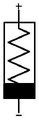
图2是本发明所采用忆阻器的电路符号。Fig. 2 is the circuit symbol of the memristor used in the present invention.
图3是本发明所采用阈值型忆阻器模型的电流-电压曲线图。FIG. 3 is a current-voltage curve diagram of a threshold-type memristor model adopted in the present invention.
图4是本发明的具体电路结构图。FIG. 4 is a specific circuit structure diagram of the present invention.
具体实施方式Detailed ways
为了使本发明的目的、技术方案及优点更加清楚明白,以下结合附图及发明实例,对本发明进一步说明。In order to make the objectives, technical solutions and advantages of the present invention clearer, the present invention will be further described below with reference to the accompanying drawings and examples of the invention.
图1是本发明的电路结构框图,整个电路包括SR忆阻锁存模块和忆阻异步置位复位模块,其中SR忆阻锁存模块由忆阻器与CMOS晶体管混合构成,电路结构简单,器件数较传统SR锁存器得到较大减少且功能齐全。忆阻异步置位复位模块由忆阻器构成的与门和或门构建而成,实现电路异步置位和复位功能。整个电路使用的器件数量小,功能齐全,且具有非易失性Figure 1 is a block diagram of the circuit structure of the present invention. The entire circuit includes an SR memristive latch module and a memristive asynchronous reset module. The SR memristive latch module is composed of a mixture of memristors and CMOS transistors. The circuit structure is simple and the device Compared with the traditional SR latch, the number of pieces is greatly reduced and the function is complete. The memristor asynchronous set and reset module is composed of an AND gate and an OR gate composed of a memristor to realize the asynchronous set and reset functions of the circuit. The entire circuit uses a small number of devices, is fully functional, and is non-volatile
图2是本发明采用Biolek提出的阈值型忆阻器模型的电路符号,假设有黑色线段一端为负端,另一端为正端。图3为Biolek阈值型忆阻器在外加正弦激励信号下的电流-电压波形。图3可以看出,该忆阻器模型具有滞回特性和阈值特性,正负电压下都各具有1个阈值:+Vt和-Vt。当忆阻器外加的正向激励电压大于正向阈值+Vt时忆阻器转换为高阻值;当反向激励电压大于负向阈值-Vt时忆阻器转换为低阻值,且在上述变化后若电压不变或者变化范围小于阈值电压,则忆阻器将会保持之前的阻值,直到忆阻器两端所加的激励电压差大于阈值,本发明中SR忆阻锁存器模块中的忆阻器利用上述的特性实现非易失特性。FIG. 2 is a circuit symbol of the present invention using the threshold-type memristor model proposed by Biolek. It is assumed that one end of a black line segment is a negative end and the other end is a positive end. Figure 3 shows the current-voltage waveform of the Biolek threshold memristor under the addition of a sinusoidal excitation signal. As can be seen from Figure 3, the memristor model has hysteresis characteristics and threshold characteristics, and each has a threshold value under positive and negative voltages: +V t and -V t . When the forward excitation voltage applied to the memristor is greater than the forward threshold +V t , the memristor switches to high resistance; when the reverse excitation voltage is greater than the negative threshold -V t , the memristor switches to low resistance, and After the above changes, if the voltage does not change or the variation range is smaller than the threshold voltage, the memristor will maintain the previous resistance value until the excitation voltage difference between the two ends of the memristor is greater than the threshold value. In the present invention, the SR memristor latches The memristor in the memory module utilizes the properties described above to achieve non-volatile properties.
图4是本发明带异步置位复位功能的CMOS混合型SR忆阻锁存器具体电路图,其中V1和V2为直流工作电源。如图4所示,该混合型SR忆阻锁存器包括第一忆阻器M1、第二忆阻器M2、第三忆阻器M3,第四忆阻器M4、第五忆阻器M5;5个NMOS晶体管:第一MOS管T1、第二MOS管T2、第三MOS管T3、第四MOS管T4、第六MOS管T6;1个PMOS晶体管:第五MOS管T5;M1、M2、M3、M4、M5均为Biolek阈值型忆阻器。第一MOS管T1、第三MOS管T3、第五MOS管T5、第六MOS管T6的栅极连接控制端CP,CP为整个电路的控制端;输入端S与第一MOS管T1的漏极相连,第一MOS管T1的源极连接第二MOS管T2的栅极;第二MOS管T2的漏极连接直流电压V1,第二MOS管T2的源极连接第四MOS管T4的漏极、第一忆阻器M1的负端、第一电阻R1的一端、第一反相器N1的输入端以及第二反相器N2的输出端;输入端R与第三MOS管T3的漏极相连,第三MOS管T3的源极连接第四MOS管T4的栅极;第四MOS管T4的源极连接至地端;第五MOS管T5的源极连接直流电压V2,第五MOS管T5的漏极连接第一忆阻器M1的正端以及第六MOS管T6的源极;第六MOS管T6的漏极连接第一反相器N1的输出端和第二反相器N2的输入端;第二忆阻器M2的负端连接第二反相器N2的输出端,第二忆阻器M2的正端连接第三忆阻器M3的正端以及第四忆阻器M4的正端;第三忆阻器M3的负端连接异步置位端SET,第五忆阻器M5的正端连接第三反相器N3的输出端,第五忆阻器M5的负端与第四忆阻器M4的负端相连,输出作为整个电路的输出端Q;整个电路的异步复位端RESET与第三反相器N3的输入端相连。结合电路结构对本发明的SR忆阻锁存器工作原理进行解析:FIG. 4 is a specific circuit diagram of the CMOS hybrid SR memristive latch with asynchronous reset function of the present invention, wherein V 1 and V 2 are DC working power supplies. As shown in FIG. 4 , the hybrid SR memristor latch includes a first memristor M 1 , a second memristor M 2 , a third memristor M 3 , a fourth memristor M 4 , and a
1、当异步置位复位端SET以及RESET均为低电平也即逻辑0,且CP为高电平时:1. When the asynchronous reset terminal SET and RESET are both low level, that is,
(1)若SR锁存器S=1,R=0时,CP=1使得第一MOS管T1、第二MOS管T2、第三MOS管T3、第六MOS管T6导通,第四MOS管T4、第五MOS管T5截止,直流电压V1经第二MOS管T2加到第一忆阻器M1的负端和第一反相器N1的输入端,此时第一忆阻器M1负端为高电平且大小近似为V1,该电压经过第一反相器N1转变为低电平,通过第六MOS管T6加到第一忆阻器M1的正端,由于阈值型忆阻器的特型,此时负端与正端电压差大于阈值的绝对值大小,导致第一忆阻器M1阻值发生变化,由初始阻值变为低阻值Ron并且保持当前阻值,第一反相器N1输入端的高电平经过第一反相器N1及第二反相器N2输入到输出端Q1,此时SR忆阻锁存器模块的输出Q1=1。第二忆阻器M2以及第三忆阻器M3构成忆阻或门,第四忆阻器M4以及第五忆阻器M5构成忆阻与门,由于异步置位复位端均为逻辑0,所以最终输出
(2)当S=0,R=1时,CP=1使得第一MOS管T1、第三MOS管T3、第四MOS管T4、第六MOS管T6导通,第二MOS管T2、第五MOS管T5截止。由于第二MOS管T2截止和第四MOS管T4导通,第一忆阻器M1负端以及第一反相器N1的输入端通过第四MOS管T4接地,此时该端为低电平,该电平在第一反相器N1的作用下转变为高电平通过第六MOS管T6加到第一忆阻器M1的正端,此时忆阻器阻值发生变换,变为高阻值Roff并且保持当前阻值,第一反相器N1输入端的低电平经过第一反相器N1和第二反相器N2输入到Q1端,此时SR忆阻锁存器模块的输出Q1=0,又由于异步置位复位端SET/RESET均为逻辑0,所以最终输出
(3)当S=0,R=0时,CP=1使得第一MOS管T1、第三MOS管T3、第六MOS管T6导通,第二MOS管T2、第四MOS管T4、第五MOS管T5截止,由于第二MOS管T2以及第四MOS管T4的截止且第一反相器N1的输入端和第二反相器N2的输出端Q1连接在一起构成锁存回路,导致此时第一忆阻器M1的负端以及第一反相器N1的输入端电压没有发生变化,因此输出端Q1输出先前的状态,第一忆阻器M1也根据锁存状态发生对应阻值的变化(若S与R变化为S=0,R=0前的时刻Q1输出为逻辑1则此时输出端Q1输出逻辑1且第一忆阻器M1阻值变化同(1),变为Ron;若变化前的时刻输出为逻辑0,则此时输。出端Q1输出逻辑0且第一忆阻器M1阻值变化同(2),变为Roff),由于异步置位复位端均为逻辑0,所以最终输出
上述(1)、(2)、(3)三种情况分别实现了SR锁存器的置1,置0,保持功能。其区别其他类似发明特点在于:利用忆阻器的记忆及阈值特性存储对应的电阻值,简化电路工作步骤,降低功耗,输出稳定,且在系统发生断电时,忆阻器中存储的电阻值保持不变从而起到断电保持的能力。The above three cases (1), (2) and (3) respectively realize the function of setting 1, setting 0, and holding the SR latch. It is different from other similar inventions in that: the memory and threshold characteristics of the memristor are used to store the corresponding resistance value, the circuit working steps are simplified, the power consumption is reduced, the output is stable, and when the system is powered off, the resistance stored in the memristor is stored. The value remains unchanged so as to have the ability to keep the power off.
2、当异步置位复位端SET/RESET均为逻辑0,且CP为低电平时:2. When the asynchronous reset terminal SET/RESET is
(1)若CP由1转变为0的时刻输出端Q1输出高电平:(1) If CP changes from 1 to 0, the output terminal Q 1 outputs a high level:
CP=0导致第一MOS管T1、第二MOS管T2、第三MOS管T3、第四MOS管T4、第六MOS管T6均截止,第五MOS管T5导通,由于V2电压略小于V1的值,再假设V2还略小于忆阻器的阈值电压,此时V2电压无法使第一忆阻器M1阻值发生变化,且由于前一时刻输出端Q1输出高电平致第一忆阻器M1负端为高电平,正端为低电平满足忆阻器阻值转变条件,阻值转变为Ron,此时根据分压原理忆阻器负端处的电压为:

(2)若CP由1转变为0的时刻输出端Q1输出低电平:(2) If CP changes from 1 to 0, the output terminal Q 1 outputs a low level:
CP=0导致第一MOS管T1、第二MOS管T2、第三MOS管T3、第四MOS管T4、第六MOS管T6均截止,第五MOS管T5导通,由于V2电压略小于V1的值,再假设V2还略小于忆阻器的阈值电压,此时V2电压无法使第一忆阻器M1阻值发生变化,且由于前一时刻输出端Q1输出低电平致第一忆阻器M1负端为低电平,正端为高电平满足忆阻器阻值转变条件,阻值转变为Roff,此时根据分压原理忆阻器负端处的电压为:

上述2种情况实现了CP为逻辑0时,输出端根据先前的输出状态保持对应状态的功能,其特点在于:利用先前忆阻器存储的阻值大小利用分压原理输出对应的逻辑电平,利用这种方法最大化简化电路结构,且工作原理不复杂,易于仿真和调整The above two cases realize that when CP is
3、异步置位复位端SET为逻辑1,RESET为逻辑0时:3. When the reset terminal SET is set asynchronously to logic 1 and RESET is logic 0:
只要SET=1,无论SR锁存器模块的输出端Q1为何值,由第二忆阻器M2和第三忆阻器M3构成的或门输出为逻辑1,此时整个电路的输出
4、异步置位复位端SET为逻辑0,RESET为逻辑1时:4. When the asynchronous reset terminal SET is
只要RESET=1,由第四忆阻器M4和第无忆阻器M5构成的与门不受前面电路的影响,输出为逻辑0即最终输出
在本发明中,电压V1、V2为直流电压,直流电压V1大小为SR锁存器输入端S和R的最高电压大小;直流电压V2的值略小于V1的值。In the present invention, the voltages V 1 and V 2 are DC voltages, and the magnitude of the DC voltage V 1 is the maximum voltage of the input terminals S and R of the SR latch; the value of the DC voltage V 2 is slightly smaller than the value of V 1 .
在本发明中,第一电阻R1的阻值需满足:Ron<<R1<<Roff(Ron为忆阻器M1的低阻值,Roff为忆阻器M1的高阻值)。In the present invention, the resistance value of the first resistor R 1 needs to satisfy: R on <<R 1 <<R off (R on is the low resistance value of the memristor M 1 , and R off is the high resistance value of the memristor M 1 resistance).
在本发明中,置位端S和复位端R以及异步置位端SET和异步复位端RESET不能同时为高电平,且上述端口在电路中均为高电平有效。In the present invention, the set terminal S and reset terminal R and the asynchronous set terminal SET and the asynchronous reset terminal RESET cannot be high level at the same time, and the above ports are all active high level in the circuit.
在本发明中,第二忆阻器M2与第三忆阻器M3构成忆阻或门,第四忆阻器M4与第五忆阻器M5构成忆阻与门,忆阻器M1、M2、M3、M4及M5的初始阻值需设定忆阻器的最小阻值Ron与最大阻值Roff之间。此后的阻值根据忆阻器两端电压差大小进行变化。In the present invention, the second memristor M 2 and the third memristor M 3 constitute a memristor OR gate, the fourth memristor M 4 and the fifth memristor M 5 constitute a memristor AND gate, and the
在本发明中,第六MOS管T6晶体管的作用在于,在CP为逻辑1时将会影响忆阻器两端电压,使得忆阻器阻值变化,在CP为逻辑0时,第六MOS管T6晶体管截止,对忆阻器状态没有影响。In the present invention, the function of the sixth MOS transistor T6 is that when CP is logic 1, it will affect the voltage across the memristor, so that the resistance value of the memristor changes. When CP is
在本发明中,对比其他类似发明,其优势在于:In the present invention, compared with other similar inventions, its advantages are:
①结构新颖且简单,所需元器件少进而一些功耗大等问题得到解决;①The structure is novel and simple, the required components are few and some problems such as high power consumption are solved;
②以本发明为基础可进一步设计其他数字逻辑电路(边沿触发器,计数器等);② On the basis of the present invention, other digital logic circuits (edge triggers, counters, etc.) can be further designed;
③在实现基本逻辑功前提下,且能实现传统SR锁存器所没有的额外的逻辑功能(异步置位复位);③Under the premise of realizing basic logic functions, it can realize additional logic functions that traditional SR latches do not have (asynchronous set reset);
本发明所提供的一种带异步置位复位功能的CMOS混合型SR忆阻锁存器,电路性能稳定,具有非易失性,电路具有异步置位和复位功能,且电路仿真测试效果良好。可根据具本发明具体电路图进行实际样品的制作。The CMOS hybrid SR memristive latch with asynchronous reset function provided by the invention has stable circuit performance, non-volatility, asynchronous set and reset functions, and good circuit simulation test effect. The actual sample can be produced according to the specific circuit diagram of the present invention.
本领域的技术人员容易理解,以上所述仅为本发明的较佳实施例,并不用以限制本发明,凡在本发明的精神和原则之内,所做的任何修改、替换和改进等,均应包含在本发明的保护范围内。Those skilled in the art can easily understand that the above are only preferred embodiments of the present invention and are not intended to limit the present invention. Any modifications, substitutions and improvements made within the spirit and principles of the present invention, etc., All should be included in the protection scope of the present invention.
Claims (6)
Priority Applications (1)
| Application Number | Priority Date | Filing Date | Title |
|---|---|---|---|
| CN202110390108.6A CN112953498B (en) | 2021-04-12 | 2021-04-12 | A CMOS Hybrid SR Memristive Latch Circuit with Asynchronous Set-Reset |
Applications Claiming Priority (1)
| Application Number | Priority Date | Filing Date | Title |
|---|---|---|---|
| CN202110390108.6A CN112953498B (en) | 2021-04-12 | 2021-04-12 | A CMOS Hybrid SR Memristive Latch Circuit with Asynchronous Set-Reset |
Publications (2)
| Publication Number | Publication Date |
|---|---|
| CN112953498A CN112953498A (en) | 2021-06-11 |
| CN112953498B true CN112953498B (en) | 2022-05-03 |
Family
ID=76231902
Family Applications (1)
| Application Number | Title | Priority Date | Filing Date |
|---|---|---|---|
| CN202110390108.6A Active CN112953498B (en) | 2021-04-12 | 2021-04-12 | A CMOS Hybrid SR Memristive Latch Circuit with Asynchronous Set-Reset |
Country Status (1)
| Country | Link |
|---|---|
| CN (1) | CN112953498B (en) |
Families Citing this family (1)
| Publication number | Priority date | Publication date | Assignee | Title |
|---|---|---|---|---|
| CN114244349A (en) * | 2021-12-06 | 2022-03-25 | 国网辽宁省电力有限公司信息通信分公司 | One-bit binary adder circuit based on memristor |
Citations (5)
| Publication number | Priority date | Publication date | Assignee | Title |
|---|---|---|---|---|
| US5051610A (en) * | 1989-02-21 | 1991-09-24 | Mitsubishi Denki Kabushiki Kaisha | SR latch circuit |
| EP1865601A1 (en) * | 2006-06-08 | 2007-12-12 | STMicroelectronics S.r.l. | Asynchronous RS flip-flop having a test mode |
| CN105741870A (en) * | 2016-01-27 | 2016-07-06 | 华中科技大学 | Nonvolatile D flip-flop circuit based on memristor |
| CN205407762U (en) * | 2016-01-27 | 2016-07-27 | 华中科技大学 | Non -volatile SR flip -flop circuit based on recall and hinder ware |
| CN112332813A (en) * | 2020-11-17 | 2021-02-05 | 杭州电子科技大学 | CMOS mixed type edge memristor D trigger circuit with asynchronous setting and resetting |
Family Cites Families (1)
| Publication number | Priority date | Publication date | Assignee | Title |
|---|---|---|---|---|
| US9628055B1 (en) * | 2015-09-24 | 2017-04-18 | Inphi Corporation | SR latch circuit with single gate delay |
-
2021
- 2021-04-12 CN CN202110390108.6A patent/CN112953498B/en active Active
Patent Citations (5)
| Publication number | Priority date | Publication date | Assignee | Title |
|---|---|---|---|---|
| US5051610A (en) * | 1989-02-21 | 1991-09-24 | Mitsubishi Denki Kabushiki Kaisha | SR latch circuit |
| EP1865601A1 (en) * | 2006-06-08 | 2007-12-12 | STMicroelectronics S.r.l. | Asynchronous RS flip-flop having a test mode |
| CN105741870A (en) * | 2016-01-27 | 2016-07-06 | 华中科技大学 | Nonvolatile D flip-flop circuit based on memristor |
| CN205407762U (en) * | 2016-01-27 | 2016-07-27 | 华中科技大学 | Non -volatile SR flip -flop circuit based on recall and hinder ware |
| CN112332813A (en) * | 2020-11-17 | 2021-02-05 | 杭州电子科技大学 | CMOS mixed type edge memristor D trigger circuit with asynchronous setting and resetting |
Non-Patent Citations (1)
| Title |
|---|
| Design and Analysis of Nonvolatile Memristor-based S-R Latch;Khaoula Mbarek;《2020 IEEE International Conference on Design & Test of Integrated Micro & Nano-Systems》;20200915;全文 * |
Also Published As
| Publication number | Publication date |
|---|---|
| CN112953498A (en) | 2021-06-11 |
Similar Documents
| Publication | Publication Date | Title |
|---|---|---|
| JP5964267B2 (en) | Nonvolatile state retention latch | |
| US8406064B2 (en) | Latching circuit | |
| TWI451698B (en) | High speed level shifter with low input voltage to wide-range high output voltage | |
| CN103051307B (en) | Memristor-based non-volatile D trigger | |
| US20170040982A1 (en) | Latch and D Flip-Flop | |
| US20180278244A1 (en) | Flip-Flop | |
| US6781411B2 (en) | Flip flop with reduced leakage current | |
| US10033356B2 (en) | Reduced power set-reset latch based flip-flop | |
| CN112953498B (en) | A CMOS Hybrid SR Memristive Latch Circuit with Asynchronous Set-Reset | |
| JP2016535487A (en) | Latch comparator circuit and method | |
| CN112332813B (en) | CMOS hybrid type edge memristor D trigger circuit with asynchronous setting and resetting | |
| US12113529B2 (en) | Electronic device and memristor-based logic gate circuit thereof | |
| US11575366B2 (en) | Low power flip-flop | |
| US12087344B2 (en) | Ferroelectric FET nonvolatile sense-amplifier-based flip-flop | |
| Sushma et al. | Low power high speed D flip flop design using improved SVL technique | |
| CN111585546B (en) | Nonvolatile latch circuit based on resistive random access memory and operation method | |
| Basford et al. | The impact of analog computational error on an analog boolean satisfiability solver | |
| JP4862161B2 (en) | Semiconductor memory circuit | |
| CN222690378U (en) | Data storage structure, chip and electronic equipment | |
| Current | Design of a quaternary latch circuit using a binary CMOS RS latch | |
| TWI858442B (en) | A register | |
| CN117674785A (en) | Low-power master-slave D flip-flop based on threshold switching memristor | |
| Nataraj et al. | Design methodology for area and energy efficient OxRAM-based non-volatile flip-flop | |
| Arundeepakvel et al. | Realization of Memristor based D-Latch | |
| Bandi et al. | Explicit pulse triggered flip flop design based on a signal feed-through scheme |
Legal Events
| Date | Code | Title | Description |
|---|---|---|---|
| PB01 | Publication | ||
| PB01 | Publication | ||
| SE01 | Entry into force of request for substantive examination | ||
| SE01 | Entry into force of request for substantive examination | ||
| GR01 | Patent grant | ||
| GR01 | Patent grant |