CN112147828B - Electronic equipment, housing assemblies, cover assemblies, and electrochromic modules - Google Patents
Electronic equipment, housing assemblies, cover assemblies, and electrochromic modules Download PDFInfo
- Publication number
- CN112147828B CN112147828B CN202010924410.0A CN202010924410A CN112147828B CN 112147828 B CN112147828 B CN 112147828B CN 202010924410 A CN202010924410 A CN 202010924410A CN 112147828 B CN112147828 B CN 112147828B
- Authority
- CN
- China
- Prior art keywords
- electrochromic module
- plastic frame
- layer
- substrate
- color
- Prior art date
- Legal status (The legal status is an assumption and is not a legal conclusion. Google has not performed a legal analysis and makes no representation as to the accuracy of the status listed.)
- Active
Links
Images


Classifications
-
- G—PHYSICS
- G02—OPTICS
- G02F—OPTICAL DEVICES OR ARRANGEMENTS FOR THE CONTROL OF LIGHT BY MODIFICATION OF THE OPTICAL PROPERTIES OF THE MEDIA OF THE ELEMENTS INVOLVED THEREIN; NON-LINEAR OPTICS; FREQUENCY-CHANGING OF LIGHT; OPTICAL LOGIC ELEMENTS; OPTICAL ANALOGUE/DIGITAL CONVERTERS
- G02F1/00—Devices or arrangements for the control of the intensity, colour, phase, polarisation or direction of light arriving from an independent light source, e.g. switching, gating or modulating; Non-linear optics
- G02F1/01—Devices or arrangements for the control of the intensity, colour, phase, polarisation or direction of light arriving from an independent light source, e.g. switching, gating or modulating; Non-linear optics for the control of the intensity, phase, polarisation or colour
- G02F1/15—Devices or arrangements for the control of the intensity, colour, phase, polarisation or direction of light arriving from an independent light source, e.g. switching, gating or modulating; Non-linear optics for the control of the intensity, phase, polarisation or colour based on an electrochromic effect
- G02F1/153—Constructional details
- G02F1/161—Gaskets; Spacers; Sealing of cells; Filling or closing of cells
-
- G—PHYSICS
- G02—OPTICS
- G02F—OPTICAL DEVICES OR ARRANGEMENTS FOR THE CONTROL OF LIGHT BY MODIFICATION OF THE OPTICAL PROPERTIES OF THE MEDIA OF THE ELEMENTS INVOLVED THEREIN; NON-LINEAR OPTICS; FREQUENCY-CHANGING OF LIGHT; OPTICAL LOGIC ELEMENTS; OPTICAL ANALOGUE/DIGITAL CONVERTERS
- G02F1/00—Devices or arrangements for the control of the intensity, colour, phase, polarisation or direction of light arriving from an independent light source, e.g. switching, gating or modulating; Non-linear optics
- G02F1/01—Devices or arrangements for the control of the intensity, colour, phase, polarisation or direction of light arriving from an independent light source, e.g. switching, gating or modulating; Non-linear optics for the control of the intensity, phase, polarisation or colour
- G02F1/15—Devices or arrangements for the control of the intensity, colour, phase, polarisation or direction of light arriving from an independent light source, e.g. switching, gating or modulating; Non-linear optics for the control of the intensity, phase, polarisation or colour based on an electrochromic effect
- G02F1/153—Constructional details
- G02F1/1533—Constructional details structural features not otherwise provided for
-
- H—ELECTRICITY
- H05—ELECTRIC TECHNIQUES NOT OTHERWISE PROVIDED FOR
- H05K—PRINTED CIRCUITS; CASINGS OR CONSTRUCTIONAL DETAILS OF ELECTRIC APPARATUS; MANUFACTURE OF ASSEMBLAGES OF ELECTRICAL COMPONENTS
- H05K5/00—Casings, cabinets or drawers for electric apparatus
- H05K5/02—Details
- H05K5/0217—Mechanical details of casings
- H05K5/0243—Mechanical details of casings for decorative purposes
-
- H—ELECTRICITY
- H05—ELECTRIC TECHNIQUES NOT OTHERWISE PROVIDED FOR
- H05K—PRINTED CIRCUITS; CASINGS OR CONSTRUCTIONAL DETAILS OF ELECTRIC APPARATUS; MANUFACTURE OF ASSEMBLAGES OF ELECTRICAL COMPONENTS
- H05K5/00—Casings, cabinets or drawers for electric apparatus
- H05K5/02—Details
- H05K5/03—Covers
Landscapes
- Physics & Mathematics (AREA)
- Nonlinear Science (AREA)
- General Physics & Mathematics (AREA)
- Optics & Photonics (AREA)
- Engineering & Computer Science (AREA)
- Microelectronics & Electronic Packaging (AREA)
- Electrochromic Elements, Electrophoresis, Or Variable Reflection Or Absorption Elements (AREA)
Abstract
Description
技术领域technical field
本发明涉及具有变色功能的电子设备的技术领域,具体是涉及一种电子设备、壳体组件、盖板组件以及电致变色模组。The invention relates to the technical field of electronic equipment with a color-changing function, in particular to an electronic equipment, a casing assembly, a cover plate assembly and an electrochromic module.
背景技术Background technique
电致变色膜片是一种常用在建筑物外玻璃以及汽车后视镜等位置的变色遮挡膜材,常规技术中的电致变色膜片的结构一般整体厚度较大。电致变色膜片内的变色材料对水氧的敏感性较高,如果对变色材料的封装不牢靠,会导致变色材料变质导致电致变色膜片的寿命降低。The electrochromic diaphragm is a kind of color-changing shielding film commonly used in the exterior glass of buildings and automobile rearview mirrors. The structure of the electrochromic diaphragm in conventional technology generally has a relatively large overall thickness. The color-changing material in the electrochromic diaphragm is highly sensitive to water and oxygen. If the packaging of the color-changing material is not reliable, the color-changing material will deteriorate and the life of the electrochromic diaphragm will be reduced.
发明内容Contents of the invention
本申请实施例第一方面提供了一种电致变色模组,所述电致变色模组包括第一基板、第一导电层、变色材料层、第二导电层、第二基板以及胶框;其中,所述第一基板、所述第一导电层、所述变色材料层、所述第二导电层以及所述第二基板依次层叠设置;所述胶框围设于所述变色材料层的侧边环周,实现对所述变色材料层的环周密封;所述胶框的水汽透过率不大于20g/m2/天。The first aspect of the embodiment of the present application provides an electrochromic module, the electrochromic module includes a first substrate, a first conductive layer, a color-changing material layer, a second conductive layer, a second substrate, and a plastic frame; Wherein, the first substrate, the first conductive layer, the color-changing material layer, the second conductive layer and the second substrate are sequentially stacked; the plastic frame surrounds the color-changing material layer The circumference of the sides realizes the circumference sealing of the color-changing material layer; the water vapor transmission rate of the plastic frame is not greater than 20g/m2/day.
第二方面,本申请实施例提供一种电致变色模组,所述电致变色模组包括第一基板、第一导电层、变色材料层、第二导电层、第二基板以及胶框;其中,所述第一基板、所述第一导电层、所述变色材料层、所述第二导电层以及所述第二基板依次层叠设置;所述胶框均围设于所述变色材料层的侧边环周,实现对所述变色材料层的环周密封;所述胶框为环氧系胶水或者丙烯酸系胶水凝固形成。In the second aspect, the embodiment of the present application provides an electrochromic module, the electrochromic module includes a first substrate, a first conductive layer, a color-changing material layer, a second conductive layer, a second substrate, and a plastic frame; Wherein, the first substrate, the first conductive layer, the color-changing material layer, the second conductive layer and the second substrate are sequentially stacked; the plastic frames are all surrounded by the color-changing material layer The circumference of the side edge is realized to seal the circumference of the color-changing material layer; the plastic frame is formed by solidification of epoxy-based glue or acrylic-based glue.
第三方面,本申请实施例提供一种电致变色模组,所述电致变色模组包括第一基板、第一导电层、变色材料层、第二导电层、第二基板以及胶框;其中,所述第一基板、所述第一导电层、所述变色材料层、所述第二导电层以及所述第二基板依次层叠设置;所述胶框均围设于所述变色材料层的侧边环周,实现对所述变色材料层的环周密封;所述胶框的宽度大于1mm,所述胶框为环氧系胶水或者丙烯酸系胶水凝固形成。In a third aspect, an embodiment of the present application provides an electrochromic module, the electrochromic module includes a first substrate, a first conductive layer, a color-changing material layer, a second conductive layer, a second substrate, and a plastic frame; Wherein, the first substrate, the first conductive layer, the color-changing material layer, the second conductive layer and the second substrate are sequentially stacked; the plastic frames are all surrounded by the color-changing material layer The circumference of the side of the color-changing material layer is realized; the width of the glue frame is greater than 1 mm, and the glue frame is formed by solidification of epoxy glue or acrylic glue.
第四方面,本申请实施例提供一种电致变色模组,所述电致变色模组包括第一基板、第一导电层、变色材料层、第二导电层、第二基板以及胶框;其中,所述第一基板、所述第一导电层、所述变色材料层、所述第二导电层以及所述第二基板依次层叠设置;所述胶框均围设于所述变色材料层的侧边环周,实现对所述变色材料层的环周密封;所述胶框内掺杂有水汽阻隔剂。In a fourth aspect, an embodiment of the present application provides an electrochromic module, the electrochromic module includes a first substrate, a first conductive layer, a color-changing material layer, a second conductive layer, a second substrate, and a plastic frame; Wherein, the first substrate, the first conductive layer, the color-changing material layer, the second conductive layer and the second substrate are sequentially stacked; the plastic frames are all surrounded by the color-changing material layer The circumference of the side edge realizes the circumference sealing of the color-changing material layer; the water vapor barrier agent is doped in the plastic frame.
第五方面,本申请实施例提供一种电致变色模组,所述电致变色模组包括第一基板、第一导电层、变色材料层、第二导电层、第二基板以及胶框;In the fifth aspect, the embodiment of the present application provides an electrochromic module, the electrochromic module includes a first substrate, a first conductive layer, a color-changing material layer, a second conductive layer, a second substrate, and a plastic frame;
其中,所述第一基板、所述第一导电层、所述变色材料层、所述第二导电层以及所述第二基板依次层叠设置;Wherein, the first substrate, the first conductive layer, the color-changing material layer, the second conductive layer and the second substrate are sequentially stacked;
所述胶框包括第一胶框和第二胶框,所述第一胶框围设于所述变色材料层的侧边环周,实现对所述变色材料层的环周密封;所述第二胶框围设于第一胶框的外周。The plastic frame includes a first plastic frame and a second plastic frame, and the first plastic frame surrounds the side circumference of the color-changing material layer to realize the circumferential sealing of the color-changing material layer; the second rubber frame The second plastic frame surrounds the outer periphery of the first plastic frame.
第六方面,本申请实施例提供一种盖板组件,所述盖板组件包括透明盖板以及上述实施例中任一项所述的电致变色模组,所述透明盖板与所述电致变色模组的第一基板贴合。In the sixth aspect, the embodiment of the present application provides a cover assembly, the cover assembly includes a transparent cover and the electrochromic module described in any one of the above embodiments, the transparent cover and the electrochromic module Bonding of the first substrate of the chromic module.
第七方面,本申请实施例提供一种壳体组件,所述壳体组件包括中框以及上述实施例中任一项所述的盖板组件;所述电致变色模组相背两侧分别与所述透明盖板以及所述中框粘接。In the seventh aspect, the embodiment of the present application provides a casing assembly, the casing assembly includes a middle frame and the cover assembly described in any one of the above embodiments; the opposite sides of the electrochromic module are respectively Bond with the transparent cover plate and the middle frame.
第八方面,本申请实施例提供一种电子设备,所述电子设备包括显示屏模组以及上述实施例中任一项所述的壳体组件;所述显示屏模组与所述盖板组件分别设于所述中框的相对两侧。In an eighth aspect, an embodiment of the present application provides an electronic device, the electronic device includes a display screen module and the housing assembly described in any one of the above embodiments; the display screen module and the cover assembly They are respectively arranged on opposite sides of the middle frame.
第九方面,本申请实施例提供一种电子设备,所述电子设备包括控制电路以及上述实施例中任一项所述的壳体组件,所述控制电路与所述壳体组件的电致变色模组耦合连接,所述控制电路用于接收控制指令,所述控制指令用于控制所述电致变色模组变色。In the ninth aspect, the embodiment of the present application provides an electronic device, the electronic device includes a control circuit and the casing assembly according to any one of the above embodiments, the control circuit and the electrochromic component of the casing assembly The modules are coupled and connected, and the control circuit is used to receive control instructions, and the control instructions are used to control the electrochromic module to change color.
本申请实施例提供的电致变色模组,通过设计和选取胶框的结构以及材质,进而保证电致变色模组整体结构具有良好的防水性能,进而稳定电致变色模组的变色性能,延长使用寿命。The electrochromic module provided in the embodiment of this application, by designing and selecting the structure and material of the plastic frame, ensures that the overall structure of the electrochromic module has good waterproof performance, thereby stabilizing the discoloration performance of the electrochromic module and prolonging the life of the electrochromic module. service life.
附图说明Description of drawings
为了更清楚地说明本发明实施例中的技术方案,下面将对实施例描述中所需要使用的附图作简单地介绍,显而易见地,下面描述中的附图仅仅是本发明的一些实施例,对于本领域普通技术人员来讲,在不付出创造性劳动的前提下,还可以根据这些附图获得其他的附图。In order to more clearly illustrate the technical solutions in the embodiments of the present invention, the drawings that need to be used in the description of the embodiments will be briefly introduced below. Obviously, the drawings in the following description are only some embodiments of the present invention. For those skilled in the art, other drawings can also be obtained based on these drawings without creative effort.
图1是本申请电致变色模组一实施例的结构断面示意图;Fig. 1 is a schematic cross-sectional view of an embodiment of the electrochromic module of the present application;
图2是电致变色模组一种实施方式的部分结构层叠示意图;Fig. 2 is a partial structural stacked schematic diagram of an embodiment of an electrochromic module;
图3是本申请电致变色模组另一实施例的结构断面示意图;Fig. 3 is a schematic cross-sectional view of another embodiment of the electrochromic module of the present application;
图4是本申请电致变色模组另一实施例的结构断面示意图;Fig. 4 is a schematic cross-sectional view of another embodiment of the electrochromic module of the present application;
图5是本申请电致变色模组又一实施例的结构断面示意图;Fig. 5 is a schematic cross-sectional view of another embodiment of the electrochromic module of the present application;
图6是本申请电致变色模组还一实施例的结构断面示意图;Fig. 6 is a schematic cross-sectional view of another embodiment of the electrochromic module of the present application;
图7是本申请电致变色模组再一实施例的结构断面示意图;Fig. 7 is a schematic cross-sectional view of another embodiment of the electrochromic module of the present application;
图8是本申请电致变色模组又一实施例的结构断面示意图;Fig. 8 is a schematic cross-sectional view of another embodiment of the electrochromic module of the present application;
图9是本申请电致变色模组还一实施例的结构断面示意图;Fig. 9 is a schematic cross-sectional view of another embodiment of the electrochromic module of the present application;
图10是本申请电致变色模组又一实施例的结构断面示意图;Fig. 10 is a schematic cross-sectional view of another embodiment of the electrochromic module of the present application;
图11是图10中电致变色模组的结构俯视示意图;Fig. 11 is a schematic top view of the structure of the electrochromic module in Fig. 10;
图12是本申请电致变色模组还一实施例的结构拆分示意图;Fig. 12 is a schematic disassembly diagram of another embodiment of the electrochromic module of the present application;
图13是图12中的绑定位置处的局部结构剖面示意图;Fig. 13 is a schematic cross-sectional view of a local structure at the binding position in Fig. 12;
图14是本申请电致变色模组另一种柔性电路板与走线绑定结构的示意图;Fig. 14 is a schematic diagram of another flexible circuit board and wiring binding structure of the electrochromic module of the present application;
图15是本申请电致变色模组又一种柔性电路板与走线绑定结构的示意图;Fig. 15 is a schematic diagram of another flexible circuit board and wiring binding structure of the electrochromic module of the present application;
图16是图15中电致变色模组的结构拆分示意图;Fig. 16 is a schematic disassembly diagram of the structure of the electrochromic module in Fig. 15;
图17是图15中A处的局部结构放大示意图;Fig. 17 is an enlarged schematic diagram of the local structure at A in Fig. 15;
图18是图15中B-B处的局部结构剖视示意图;Fig. 18 is a schematic cross-sectional view of a partial structure at B-B in Fig. 15;
图19是本申请电致变色模组又一实施例的结构断面示意图;Fig. 19 is a schematic cross-sectional view of another embodiment of the electrochromic module of the present application;
图20是本申请电致变色模组另一实施例的局部结构断面示意图;Fig. 20 is a schematic cross-sectional view of a partial structure of another embodiment of the electrochromic module of the present application;
图21是本申请电致变色模组还一实施例的局部结构断面示意图;Fig. 21 is a schematic cross-sectional view of a partial structure of another embodiment of the electrochromic module of the present application;
图22是本申请电致变色模组又一实施例的局部结构断面示意图;Fig. 22 is a schematic cross-sectional view of a partial structure of another embodiment of the electrochromic module of the present application;
图23是本申请电致变色模组封装方法一实施例的流程示意图;Fig. 23 is a schematic flow chart of an embodiment of an electrochromic module packaging method of the present application;
图24是电致变色模组层叠结构(半成品)的结构层叠示意图;Fig. 24 is a structural stacking diagram of the stacked structure (semi-finished product) of the electrochromic module;
图25是在电致变色模组半成品上形成环槽后的结构层叠示意图;Fig. 25 is a schematic diagram of structural lamination after ring grooves are formed on the semi-finished electrochromic module;
图26是图25的结构俯视示意图;Fig. 26 is a schematic top view of the structure of Fig. 25;
图27是在电致变色模组半成品的环槽内填充密封胶后的结构示意图;Fig. 27 is a schematic diagram of the structure after filling the sealant in the ring groove of the semi-finished electrochromic module;
图28是本申请电致变色模组封装方法另一实施例的流程示意图;Fig. 28 is a schematic flow chart of another embodiment of the electrochromic module packaging method of the present application;
图29是本申请电致变色模组封装方法又一实施例的流程示意图;Fig. 29 is a schematic flow chart of another embodiment of the electrochromic module packaging method of the present application;
图30是在电致变色模组半成品上形成两圈环槽后的结构层叠示意图;Fig. 30 is a schematic diagram of the structural lamination after forming two ring grooves on the semi-finished electrochromic module;
图31是图30的结构俯视示意图;Figure 31 is a schematic top view of the structure of Figure 30;
图32是电致变色模组另一种双胶框的结构示意图;Fig. 32 is a schematic structural diagram of another double glue frame of the electrochromic module;
图33是本申请盖板组件一实施例的结构示意图;Fig. 33 is a schematic structural view of an embodiment of the cover assembly of the present application;
图34是本申请盖板组件另一实施例的结构示意图;Fig. 34 is a schematic structural view of another embodiment of the cover assembly of the present application;
图35是本申请盖板组件又一实施例的结构示意图;Fig. 35 is a schematic structural view of another embodiment of the cover assembly of the present application;
图36是盖板组件单侧引线绑定的结构示意图;Fig. 36 is a structural schematic diagram of one-side lead wire binding of the cover plate assembly;
图37是本申请盖板组件另一实施例的结构断面示意图;Fig. 37 is a schematic cross-sectional view of another embodiment of the cover assembly of the present application;
图38是本申请盖板组件再一实施例的结构断面示意图;Fig. 38 is a schematic cross-sectional view of another embodiment of the cover assembly of the present application;
图39是图38实施例中盖板组件装配方法一实施例的流程示意图;Fig. 39 is a schematic flowchart of an embodiment of the method for assembling the cover assembly in the embodiment of Fig. 38;
图40是电致变色模组与透明盖板贴合后并点胶的结构示意图;Fig. 40 is a schematic diagram of the structure of the electrochromic module and the transparent cover after bonding and dispensing glue;
图41是常规技术中电子设备的后盖板与中框粘接的结构示意图;Fig. 41 is a schematic structural diagram of bonding the back cover and the middle frame of the electronic device in the conventional technology;
图42是本申请壳体组件一实施例的结构剖面示意图;Fig. 42 is a schematic cross-sectional view of an embodiment of the shell assembly of the present application;
图43是图42中壳体组件的结构正视示意图;Fig. 43 is a schematic front view of the structure of the housing assembly in Fig. 42;
图44是本申请电子设备一实施方式的局部结构组成框图;Fig. 44 is a block diagram of a partial structure composition of an embodiment of the electronic device of the present application;
图45是本申请电子设备另一实施方式的结构组成框图;Fig. 45 is a structural composition block diagram of another embodiment of the electronic device of the present application;
图46是本申请电子设备还一实施方式的结构组成框图;Fig. 46 is a structural block diagram of another embodiment of the electronic device of the present application;
图47是电子设备一实施方式的结构示意图;Fig. 47 is a schematic structural diagram of an embodiment of an electronic device;
图48是电子设备的一种操作状态的示意图;Fig. 48 is a schematic diagram of an operating state of an electronic device;
图49是电子设备的另一种操作状态的示意图;Fig. 49 is a schematic diagram of another operating state of the electronic device;
图50是是电致变色模组失效情况下出现反向着色色块的结构示意图;Fig. 50 is a structural schematic diagram of a reversely colored color block in the case of failure of the electrochromic module;
图51是当电致变色模组胶框的断裂伸长率不足导致粘接不到位的示意图。Fig. 51 is a schematic diagram of insufficient bonding of the plastic frame of the electrochromic module due to insufficient elongation at break.
具体实施方式Detailed ways
下面结合附图和实施例,对本发明作进一步的详细描述。特别指出的是,以下实施例仅用于说明本发明,但不对本发明的范围进行限定。同样的,以下实施例仅为本发明的部分实施例而非全部实施例,本领域普通技术人员在没有做出创造性劳动前提下所获得的所有其它实施例,都属于本发明保护的范围。The present invention will be described in further detail below in conjunction with the accompanying drawings and embodiments. In particular, the following examples are only used to illustrate the present invention, but not to limit the scope of the present invention. Likewise, the following embodiments are only some but not all of the embodiments of the present invention, and all other embodiments obtained by persons of ordinary skill in the art without creative efforts fall within the protection scope of the present invention.
本发明中的术语“第一”、“第二”、“第三”仅用于描述目的,而不能理解为指示或暗示相对重要性或者隐含指明所指示的技术特征的数量。由此,限定有“第一”、“第二”、“第三”的特征可以明示或者隐含地包括至少一个该特征。本发明的描述中,“多个”的含义是至少两个,例如两个,三个等,除非另有明确具体的限定。本发明实施例中所有方向性指示(诸如上、下、左、右、前、后……)仅用于解释在某一特定姿态(如附图所示)下各部件之间的相对位置关系、运动情况等,如果该特定姿态发生改变时,则该方向性指示也相应地随之改变。本申请实施例中的术语“包括”和“具有”以及它们任何变形,意图在于覆盖不排他的包含。例如包含了一系列步骤或单元的过程、方法、系统、产品或设备没有限定于已列出的步骤或单元,而是可选地还包括没有列出的步骤或单元,或可选地还包括对于这些过程、方法、产品或设备固有的其它步骤或组件。The terms "first", "second", and "third" in the present invention are only used for descriptive purposes, and cannot be understood as indicating or implying relative importance or implicitly specifying the quantity of indicated technical features. Thus, features defined as "first", "second", and "third" may explicitly or implicitly include at least one of these features. In the description of the present invention, "plurality" means at least two, such as two, three, etc., unless otherwise specifically defined. All directional indications (such as up, down, left, right, front, back...) in the embodiments of the present invention are only used to explain the relative positional relationship between the components in a certain posture (as shown in the accompanying drawings) , sports conditions, etc., if the specific posture changes, the directional indication also changes accordingly. The terms "comprising" and "having" and any variations thereof in the embodiments of the present application are intended to cover non-exclusive inclusion. For example, a process, method, system, product or device comprising a series of steps or units is not limited to the listed steps or units, but optionally also includes unlisted steps or units, or optionally further includes For other steps or components inherent in those processes, methods, products, or devices.
在本文中提及“实施例”意味着,结合实施例描述的特定特征、结构或特性可以包含在本发明的至少一个实施例中。在说明书中的各个位置出现该短语并不一定均是指相同的实施例,也不是与其它实施例互斥的独立的或备选的实施例。本领域技术人员显式地和隐式地理解的是,本文所描述的实施例可以与其它实施例相结合。Reference herein to an "embodiment" means that a particular feature, structure, or characteristic described in connection with the embodiment can be included in at least one embodiment of the present invention. The occurrences of this phrase in various places in the specification are not necessarily all referring to the same embodiment, nor are separate or alternative embodiments mutually exclusive of other embodiments. It is understood explicitly and implicitly by those skilled in the art that the embodiments described herein can be combined with other embodiments.
作为在此使用的“电子设备”(或简称为“终端”)包括,但不限于被设置成经由有线线路连接(如经由公共交换电话网络(PSTN)、数字用户线路(DSL)、数字电缆、直接电缆连接,以及/或另一数据连接/网络)和/或经由(例如,针对蜂窝网络、无线局域网(WLAN)、诸如DVB-H网络的数字电视网络、卫星网络、AM-FM广播发送器,以及/或另一通信终端的)无线接口接收/发送通信信号的装置。被设置成通过无线接口通信的通信终端可以被称为“无线通信终端”、“无线终端”或“移动终端”。移动终端的示例包括,但不限于卫星或蜂窝电话;可以组合蜂窝无线电电话与数据处理、传真以及数据通信能力的个人通信系统(PCS)终端;可以包括无线电电话、寻呼机、因特网/内联网接入、Web浏览器、记事簿、日历以及/或全球定位系统(GPS)接收器的PDA;以及常规膝上型和/或掌上型接收器或包括无线电电话收发器的其它电子装置。手机即为配置有蜂窝通信模块的电子设备。"Electronic equipment" (or simply "terminal") as used herein includes, but is not limited to, configured to direct cable connection, and/or another data connection/network) and/or via (for example, for cellular networks, wireless local area networks (WLAN), digital television networks such as DVB-H networks, satellite networks, AM-FM broadcast transmitters , and/or a device for receiving/sending communication signals via a wireless interface of another communication terminal. A communication terminal arranged to communicate over a wireless interface may be referred to as a "wireless communication terminal", "wireless terminal" or "mobile terminal". Examples of mobile terminals include, but are not limited to, satellite or cellular telephones; Personal Communications Systems (PCS) terminals that may combine cellular radiotelephones with data processing, facsimile, and data communication capabilities; may include radiotelephones, pagers, Internet/Intranet access , a PDA with a web browser, organizer, calendar, and/or Global Positioning System (GPS) receiver; and a conventional laptop and/or palm-type receiver or other electronic device including a radiotelephone transceiver. A mobile phone is an electronic device equipped with a cellular communication module.
本申请实施例首先是提出了一种基于电致变色技术的电致变色模组的结构。该电致变色模组中的电致变色材料基于有机聚合物,譬如包括聚苯胺、聚噻吩等。The embodiment of the present application first proposes a structure of an electrochromic module based on electrochromic technology. The electrochromic material in the electrochromic module is based on organic polymers, such as polyaniline and polythiophene.
电致变色材料因为是基于电化学反应而产生的变色效应,电化学反应对水氧要求非常严格,一旦有少量的水氧侵入,材料中发生电解水反应,产生高活性的氧气,将对材料的变色性能不可逆的破坏,导致材料氧化发黄甚至完全失效的问题。因此对电致变色材料的密封状况成为了电致变色模组结构的关键所在。Electrochromic materials are based on the color-changing effect produced by electrochemical reactions. Electrochemical reactions have very strict requirements on water and oxygen. Once a small amount of water and oxygen invades, electrolysis of water will occur in the material to generate highly active oxygen, which will damage the material. The irreversible damage to the discoloration performance of the material will lead to the problem of oxidative yellowing or even complete failure of the material. Therefore, the sealing condition of the electrochromic material becomes the key to the structure of the electrochromic module.
请参阅图1,图1是本申请电致变色模组一实施例的结构断面示意图;本实施例中的电致变色模组100包括第一基板110、第一导电层120、变色材料层130、第二导电层140、第二基板150以及胶框160。Please refer to FIG. 1. FIG. 1 is a schematic cross-sectional view of an embodiment of the electrochromic module of the present application; the
具体而言,所述第一基板110、所述第一导电层120、所述变色材料层130、所述第二导电层140以及所述第二基板150依次层叠设置;在本实施例中,所述胶框160围设于所述变色材料层130设置,胶框160的两端分别与所述第一导电层120以及所述第二导电层140的表面粘接。Specifically, the
可选地,在本实施例中,第一基板110和第二基板150的材质为柔性透明树脂材料,进而使得电致变色模组100整体结构为柔性可弯曲的结构形式。第一基板110和第二基板150起到支撑和保护内部结构的作用。在一些实施例中,第一基板110和第二基板150的材质可以为PET(Polyethylene terephthalate简称PET或PEIT,俗称涤纶树脂,对苯二甲酸与乙二醇的缩聚物)、PMMA(聚甲基丙烯酸甲酯(poly(methyl methacrylate)),简称PMMA),又称做压克力、亚克力(英文Acrylic)或有机玻璃)、PC(Polycarbonate,聚碳酸酯(英文简称PC)是分子链中含有碳酸酯基的高分子聚合物)、PI(聚酰亚胺(Polyimide))等。关于第一基板110和第二基板150的更多材料类型,在本领域技术人员的理解范围内,此处不再一一列举并详述。其中,第一导电层120和第二导电层140的形成方法则可以是物理气相沉积(PVD,Physical Vapor Deposition),具体包括真空蒸发、溅射、离子镀(空心阴极离子镀、热阴极离子镀、电弧离子镀、活性反应离子镀、射频离子镀、直流放电离子镀)等。Optionally, in this embodiment, the material of the
其中,第一导电层120以及第二导电层140的厚度可是分别在100nm-300nm之间,具体可以为100nm、120nm、150nm、200nm、280nm以及300nm等。第一导电层120和第二导电层140的材质由透明导电材料制成。透明导电材料可以为铟锡氧化物(ITO)、锌铝氧化物(AZO)氧化锡掺氟(FTO)或者石墨烯薄膜等。Wherein, the thickness of the first
请参阅图2,图2是电致变色模组一种实施方式的部分结构层叠示意图,其中,变色材料层130还包括亚层结构,如图2中所示,变色材料层130包括夹设于第一导电层120和第二导电层140之间且依次层叠设置的电致变色层(也即EC层)131,电介质层132,以及离子储存层(也即IC层)133。可选地,电致变色层131的材料可以选自有机聚合物(包括聚苯胺、聚噻吩等)、无机材料(普鲁士蓝、过渡金属氧化物,如三氧化钨)以及有机小分子(紫罗精)等。本申请实施例中以电致变色层131为有机聚合物为例进行说明,电致变色层131具体可以为固态或者凝胶态材料。可选地,该离子储存层133和电介质层132可以是通过PVD的方式形成,电致变色层131(其中,该电致变色层131即为前文所述的有机聚合物或者无机材料)可以是通过刮涂或者滴灌等方式形成,关于这部分详细的技术特征,在本领域技术人员的理解范围内,此处亦不再详述。Please refer to FIG. 2. FIG. 2 is a schematic diagram of partial structural lamination of an embodiment of an electrochromic module, wherein the color-changing
另外,电致变色层131还可以以有机小分子为电解质材料。而电致变色层131为有机小分子时,具体的形成方式可以是在第一导电层120和第二导电层140之间通过真空灌装工艺形成,此处亦不再详细介绍。In addition, the
请参阅图3,图3是本申请电致变色模组另一实施例的结构断面示意图;与前述实施例不同的是,在本实施例中的电致变色模组是一种大小片的结构。具体而言,所述胶框160围设于所述第一导电层120、所述变色材料层130、所述第二导电层140以及所述第二基板150的侧边环周并与所述第一基板110朝向所述第一导电层120的表面粘接。Please refer to Figure 3, Figure 3 is a schematic cross-sectional view of another embodiment of the electrochromic module of the present application; different from the previous embodiment, the electrochromic module in this embodiment is a structure of large and small pieces . Specifically, the
可选地,请参阅图4,图4是本申请电致变色模组另一实施例的结构断面示意图;本实施例中的电致变色模组100同样包括第一基板110、第一导电层120、变色材料层130、第二导电层140、第二基板150以及胶框160;与前述实施例不同的是,本实施例中的电致变色模组100还包括水氧阻隔单元170。Optionally, please refer to FIG. 4. FIG. 4 is a schematic cross-sectional view of another embodiment of the electrochromic module of the present application; the
在一些实施例中,水氧阻隔单元170与所述第二基板150背离所述第二导电层140的表面贴合。所述水氧阻隔单元170的面积大于所述第二基板150的面积,所述水氧阻隔单元170与所述第二基板150背离所述第二导电层140的一侧表面以及所述胶框160远离所述第一基板110的端面粘接;即胶框160的相对两端分别与所述第一基板110以及所述水氧阻隔单元170粘接。水氧阻隔单元170可以是通过光学胶层1701(OCA(Optically ClearAdhesive))与第二基板150背粘接。具体地,第二基板150和水氧阻隔单元170之间可以采用UV或其他液态胶水进行封装。In some embodiments, the water and
可选地,该水氧阻隔单元170包括基材171以及镀设于所述基材171至少一侧表面的水氧阻隔层172。其中,所述基材171可以是采用柔性透明树脂材料制成,包括聚对苯二甲酸乙二醇酯PET、聚碳酸酯PC、聚酰亚胺PI等。所述水氧阻隔层172可以为为致密金属氧化物层或者无机非金属层或者有材料与无机材料叠加的复合层。譬如氧化铝、硅氧化物或者多种材料的叠层复合结构等。其中,本实施例中的水氧阻隔单元170为具有镀有水氧阻隔层172的柔性基材,其水汽透过率WVTR<1x10⁻²g/m2/day。其中,本申请实施例中水氧阻隔单元170的水汽透过方向为从水氧阻隔单元170的一侧表面在厚度方向上渗透经过水氧阻隔单元170达到相对另一侧表面的物理表征。Optionally, the water and
请继续参阅图4,在结构上,电致变色模组中第二基板150的尺寸小于第一基板110尺寸也小于水氧阻隔单元170的尺寸。如此,可以利用第一基板110和水氧阻隔单元170之间的胶框160,形成环形包围,将电致变色单元的核心层电致变色材料保护,防止水氧侵入。Please continue to refer to FIG. 4 , structurally, the size of the
请参阅图5,图5是本申请电致变色模组又一实施例的结构断面示意图;在本实施例中,第二基板150和水氧阻隔单元170之间,还有一层光学胶层1701粘结。光学胶层1701可以提高第二基板150和水氧阻隔单元170的粘结力,同时避免二者之间形成空气层,即避免胶框160之中密封进气体,因为密封的气体会在温度升高时膨胀,影响电致变色材料的可靠性。Please refer to Figure 5, Figure 5 is a schematic cross-sectional view of another embodiment of the electrochromic module of the present application; in this embodiment, there is an
可选地,在本实施例中,所述胶框160的水汽透过率不大于20g/m2/天。水蒸气透过率实际上包含了水蒸气透过量和水蒸气透过系数两个含义,这两个含义所表达的意思也有一定的区别,但都可以用来表示水蒸气透过某种材料的能力。水蒸气透过量表示在一定的时间,一定的温度和湿度条件下,水蒸气透过材料的重量。水蒸气透过率则是通过系数换算的水蒸气透过量的标准值,并对应标准单位,用于不同测试结果之间的比较。水蒸气透过量和水蒸气透过系数按照GB/T 1037-1988《塑料薄膜和片材透水蒸气性试验方法---杯式法》(对应美国试验与协会标准ASTM E96-1980)进行测定。具体的测定条件以及测定方式此处不做具体限定。其中,本申请实施例中胶框160的水汽透过方向为从胶框160的外侧表面在厚度T的方向上渗透经过胶框160达到与变色材料层130相邻一侧表面的物理表征。Optionally, in this embodiment, the water vapor transmission rate of the
可选地,胶框160可以采用环氧系胶水或者丙烯酸系胶水凝固形成。其中,环氧系胶水具有更好的防水性能,而丙烯酸系胶水的粘接力则更强。请参阅下表(表一),下表是胶框在不同的条件下的水汽透过率测试数据情况。Optionally, the
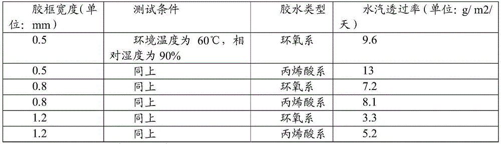
为保证防水的可靠性以及有效,本实施例中的胶框160的宽度T可以为大于1mm。具体可以为1.1mm、1.2mm、1.5mm、2mm、3mm等,具体数值不做具体限定,此处亦不再一一列举。需要说明的是,这里所说的胶框160的宽度T大于1mm也不是说越大越好,当满足水汽阻隔性能要求后,还需要考虑电致变色模组的整体黑边(不可变色区域宽度)的问题,一般来讲,胶框160的宽度T也会控制在10mm以内。In order to ensure the reliability and effectiveness of waterproofing, the width T of the
本实施例中的胶框要求:在环境温度为60℃,相对湿度为90%(指空气中水汽压与相同温度下饱和水汽压的百分比。或湿空气的绝对湿度与相同温度下可能达到的最大绝对湿度之比。也可表示为湿空气中水蒸气分压力与相同温度下水的饱和压力之比,相对湿度(Relative Humidity),用RH表示。表示空气中的绝对湿度与同温度和气压下的饱和绝对湿度的比值,得数是一个百分比。(也就是指某湿空气中所含水蒸气的质量与同温度和气压下饱和空气中所含水蒸气的质量之比,这个比值用百分数表示。例如,本申请实施例中的实验条件所说的湿度为90%,即指相对湿度。))的条件下:胶框160的水汽透过率为1-15g/m2/天。通过限定胶框160的水汽透过率可以保证变色材料不被污染,不会发生反向着色(具体什么是反向着色将在后文详细解释)的问题,进而稳定电致变色模组的变色性能,延长使用寿命。The plastic frame requirement in the present embodiment: be 60 ℃ at ambient temperature, and relative humidity is 90% (referring to the percentage of saturated water vapor pressure in the water vapor pressure in the air and the same temperature. Or the absolute humidity of wet air and the possible reach under the same temperature The ratio of the maximum absolute humidity. It can also be expressed as the ratio of the partial pressure of water vapor in humid air to the saturation pressure of water at the same temperature. The ratio of the saturated absolute humidity, the result is a percentage. (That is to say, the ratio of the mass of water vapor contained in a certain humid air to the mass of water vapor contained in the saturated air at the same temperature and pressure, this ratio is expressed in percentage For example, the humidity mentioned in the experimental conditions in the embodiments of the present application is 90%, which refers to the relative humidity.)) Under the conditions: the water vapor transmission rate of the
可选地,本实施例中胶框160的断裂伸长率(断裂伸长率一般用断裂时的相对伸长率,即胶框断裂时的伸长与其初始长度之比,以百分率表示。它是表征胶框柔软性能和弹性性能的指标。断裂伸长率越大表示其柔软性能和弹性越好。)为2-400%,或者模量<1Gpa(这里所说的模量指的是模量是指材料在受力状态下应力与应变之比。模量的倒数称为柔量。意义:弹性模量可视为衡量材料产生弹性变形难易程度的指标,其值越大,使材料发生一定弹性变形的应力也越大,即材料刚度越大,亦即在一定应力作用下,发生弹性变形越小)。本申请实施例中之所以对胶框160的断裂伸长率有要求,其目的是需要保证在电致变色模组柔性形变或者弯折过程中胶框具有稳定的结构状态,不会使胶框密封失效。Optionally, the elongation at break of the
可选地,胶框160与其他结构层之间的粘接界面可以做一定的处理,譬如粘接界面在图4实施例中胶框160的相对两端分别与第一基板110以及水氧阻隔单元170的粘接接触面;在图1实施例中为胶框160的相对两端分别与第一导电层120以及第二导电层140粘接接触面。粘接界面的具体处理方式包括等离子处理、粗化或者印刷油墨层等,目的都是提高胶框160与其他结构层之间的粘接强度,水汽侵入主要不是从粘接界面侵入,而是从胶框160的本体侵入。胶框160和下层(水氧阻隔膜)以及上层(PET/ITO膜)形成牢靠的粘接即可。而关于胶框160与其他结构层之间的具体的粘接力将在后文中介绍。Optionally, the adhesive interface between the
可选地,胶框160内还可以掺杂有水汽阻隔剂,具体可以是在胶框160的形成过程中的胶水中添加。水汽阻隔剂在所述胶框160中的质量分数为1-10%。具体可以为1%、3%、5%、8%、10%等,在不影响胶框160强度的情况下可以适当增加水汽阻隔剂的质量分数比例。具体地,可以是胶水内部可以加入一些spacer,质量分数1-10%左右比例,用于阻隔水汽的路径;或者加入一定量的分子筛,用来吸附水汽,延缓寿命。其中,Spacer主要成分是SiO2,微米级SiO2微米球。分子筛是化学中的一个常见概念,具体成分为水合硅铝酸盐(泡沸石)或天然沸石等。Spacer因为是SiO2微米球,可以阻挡水汽,分子筛可以吸收水汽。二者可以单独添加使用,也可以共同添加使用。Optionally, a moisture barrier agent may also be doped in the
请参阅图6,图6是本申请电致变色模组还一实施例的结构断面示意图;本实施例中的电致变色模组100同样包括依次层叠设置的第一基板110、第一导电层120、变色材料层130、第二导电层140、第二基板150以及水氧阻隔单元170;与前述实施例不同的是,本实施例中的胶框160包括第一胶框161和第二胶框162,所述第一胶框161围设于所述变色材料层130的侧边环周,所述第二胶框162围设于第一胶框161的外周。需要说明的是,本申请关于胶框的结构、材料以及性能的描述不限于图示实施例中的具体位置,因本文说明书篇幅限制,本申请实施例仅以一种或者几种胶框位置结构进行说明,这不应该造成对本申请范围造成限定,本领域技术人员可以在本申请实施例的技术思想(双胶框以及多胶框)之下做出一些结构的改进,均应在本申请的保护范围之内。本实施例中是在图4实施例的基础上做的双胶框或者多胶框结构的变形,当然,关于双胶框或者多胶框结构的思想,可以结合在图1实施例以及后续其他实施例结构中,此处作此说明。Please refer to FIG. 6. FIG. 6 is a schematic cross-sectional view of another embodiment of the electrochromic module of the present application; the
可选地,所述第一胶框161更加靠近变色材料层130,因此可以为第一胶框161的水汽透过率低于所述第二胶框162的水汽透过率。而所述第二胶框162的粘接性可以高于所述第一胶框161的粘接性。这里所说的粘接性指的是胶框与其他结构层的粘接界面(本图示实施例中具体为胶框与第一基板110以及水氧阻隔单元170之间的粘接界面)之间的粘接牢靠程度,也即不易剥离的程度。该性能反映胶框与其他结构层的粘接可靠性或者牢固性。Optionally, the
本实施例的技术方案中采用两层胶框的结构,对外侧的胶框162的要求其水氧阻隔性可以略低,具体可以为胶框162的水汽透过率不大于20g/m2/天;对外侧胶框162的粘接力要高一些,对其断裂伸长率有要求,需要满足断裂伸长率在2-400%;而内侧胶框161的水氧阻隔性要求高,具体要求内侧胶框161的水汽透过率不大于15g/m2/天,而对内侧胶框161的粘接力可以要求较低。可选地,内侧胶框161可以采用防水性高的环氧体系胶水,而外侧胶框162则可以采用粘接性比较好的丙烯酸体系胶水。In the technical solution of this embodiment, a two-layer plastic frame structure is adopted, and the water and oxygen barrier property of the outer
双胶框方案的背景是:在实际应用中,某些窄边框和3D曲面贴合的要求下,胶框变窄,很难寻找到阻隔水汽同时粘接力能满足3D贴合要求的胶水。例如如果仅仅使用环氧胶,环氧胶水汽透过率较好,但是环氧胶和PET以及水氧阻隔膜粘接力相对较弱,并且胶水较硬,不能很好的满足3D贴合的需求;如果仅仅使用丙烯酸体系胶水或者其他粘接力较好并且较软的胶水,这种胶水在胶框宽度一定的情况下(考虑黑边的问题),防水性能又不能很好的满足要求,本申请实施例的技术方案中,内侧采用防水性较好的环氧体系胶水+外侧粘结性较好的丙烯酸体系胶水的双胶框方案则很好的解决了上述问题。请参阅下表(表二),下表是双胶框方案与单胶框的测试实验对比数据。The background of the double glue frame solution is: in practical applications, under the requirements of certain narrow frames and 3D surface bonding, the glue frame becomes narrower, and it is difficult to find glue that can block moisture and meet the requirements of 3D bonding. For example, if only epoxy glue is used, the water vapor transmission rate of epoxy glue is better, but the adhesion between epoxy glue and PET and water oxygen barrier film is relatively weak, and the glue is hard, which cannot meet the requirements of 3D bonding. Requirements; if only acrylic glue or other glue with good adhesion and softness is used, the waterproof performance of this kind of glue cannot meet the requirements well when the width of the glue frame is fixed (considering the problem of black borders), In the technical solution of the embodiment of the present application, the double-frame solution of epoxy system glue with better water resistance + acrylic system glue with better adhesion on the outside can well solve the above problems. Please refer to the table below (Table 2). The table below shows the comparison data of the test experiment between the double glue frame scheme and the single glue frame scheme.

注:上表中的实验数据,双胶框的水汽透过率指的是水汽从外侧胶框(第二胶框162)的外表面渗透经过外侧胶框以及内侧胶框(第一胶框161)到达内胶框内侧表面的物理表征。Note: For the experimental data in the above table, the water vapor transmission rate of the double rubber frame refers to the water vapor permeating from the outer surface of the outer rubber frame (the second rubber frame 162) through the outer rubber frame and the inner rubber frame (the first rubber frame 161 ) to the physical characterization of the inner surface of the inner rubber frame.
从以上分析对比可知,双胶框方案中,当第一胶框161和第二胶框162的宽度(T1、T2)均为0.3mm时,可以满足胶框整体(第一胶框161和第二胶框162)的水汽透过率不大于20g/m2/天的要求。当双胶框的宽度均为0.5时,防水性能优于环氧系单胶框宽度为0.8的方案。From the above analysis and comparison, it can be seen that in the double-plastic frame scheme, when the widths (T1, T2) of the first
可选地,为了保证双胶框方案具备良好的防水以及粘接性能,本实施例中的所述第一胶框161的宽度T1和所述第二胶框162的宽度T2设计为均大于0.3mm。其中,第一胶框161和所述第二胶框162可以是间隔设置也可以是接触设置,关于胶框的形成方式将在后续实施例中具体描述。Optionally, in order to ensure that the double rubber frame solution has good waterproof and adhesive performance, the width T1 of the
请参阅图7,图7是本申请电致变色模组再一实施例的结构断面示意图;本实施例中的电致变色模组100同样包括依次层叠设置的第一基板110、第一导电层120、变色材料层130、第二导电层140、第二基板150以及水氧阻隔单元170;与前述实施例不同的是,本实施例中的胶框160包括第一胶框161、第二胶框162以及第三胶框163,所述第一胶框161围设于所述变色材料层130的侧边环周,所述第二胶框162围设于第一胶框161的外周,而所述第三胶框163设于所述第二胶框162的外周。Please refer to FIG. 7. FIG. 7 is a schematic cross-sectional view of another embodiment of the electrochromic module of the present application; the
本实施例的技术方案可以是在上一实施例的基础上增加第三胶框163,具体可以是如图7中所示在第二胶框162的外周设置第三胶框163,还可以是如图8中的结构,图8是本申请电致变色模组又一实施例的结构断面示意图;图8中的结构相当于在电致变色模组整体结构的外围增加了一层胶框(第三胶框163),本实施例中通过增加第三胶框163的结构,可以进一步加强电致变色模组整体的防水性能。其中,第三胶框163的材料可以是选取与第一胶框161相同的环氧系胶水凝固形成,还可以是纳米疏水材料,譬如聚四氟乙烯、氟化聚乙烯、氟碳蜡等。第三胶框163也可以是在第二胶框162外周贴设的防水泡棉等。其中,要求第三胶框163的水汽透过率不大5g/m2/天。请参阅下表(表三),下表是双胶框方案与三胶框方案的测试实验对比数据。The technical solution of this embodiment may be to add a third

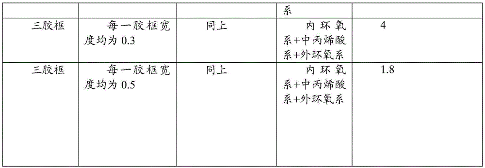
从以上实验数据可知,在胶框宽度均为0.3mm的情况下,三胶框的方案的防水性能明显优于双胶框的方案。在本实施例中,综合考虑粘接性以及防水性能,第三胶框163的宽度同样可以是大于0.3mm。具体可以为0.31mm、0.4mm、0.5mm、0.8mm、1mm等,此处不做具体限定。关于第三胶框163其他的性能参数可以参照前述实施例中的第一胶框161,此处不再赘述。From the above experimental data, it can be known that the waterproof performance of the solution with three rubber frames is obviously better than that of the solution with double rubber frames when the width of the plastic frames is all 0.3mm. In this embodiment, the width of the third
请参阅图9,图9是本申请电致变色模组还一实施例的结构断面示意图;与前述图4实施例不同的是,本实施例中的水氧阻隔单元170包括基材171、水氧阻隔层172以及外观膜层173。可选地,水氧阻隔层172和外观膜层173分别设于基材171的相对两侧。其中,外观膜层173用于实现不同的外观效果,具体可以包括纹理层(可以通过UV转印的方式形成)、色彩镀膜层(可以通过NCVM(Non conductive vacuum metalization的缩写,又称不连续镀膜技术或不导电电镀技术)的方式形成)、纳米压印层、色彩镀膜层、渐变色效果层、油墨层以及光油保护层等的一种或者多种的组合,此处不做具体限定。本实施例中电致变色模组的总体(第一基板110、第一导电层120、变色材料层130、第二导电层140、第二基板150以及水氧阻隔单元170层叠在一起)厚度可以为200-300um。Please refer to Figure 9, Figure 9 is a schematic cross-sectional view of another embodiment of the electrochromic module of the present application; different from the embodiment in Figure 4, the water and
请参阅图10,图10是本申请电致变色模组又一实施例的结构断面示意图;本实施例中的电致变色模组还包括金属走线180,金属走线180具体包括第一金属走线181以及第二金属走线182;所述第一金属走线181与所述第一导电层120连接,所述第二金属走线182与所述第二导电层140连接。其中,金属走线180包括但不限于银浆线、镀铜、镀铝、或者钼铝钼等多层走线结构。Please refer to FIG. 10. FIG. 10 is a schematic cross-sectional view of another embodiment of the electrochromic module of the present application; the electrochromic module in this embodiment also includes a
请一并参阅图11,图11是图10中电致变色模组的结构俯视示意图。所述第一金属走线181沿靠近所述第一导电层120表面的边沿位置设置,所述第二金属走线182沿靠近所述第二导电层150表面的边沿位置设置。其中,走线的具体结构有多种设计形式,如L形走线(本实施例中图示的情况)、环形走线等,此处不做具体限定。Please also refer to FIG. 11 . FIG. 11 is a schematic top view of the structure of the electrochromic module in FIG. 10 . The
为了使得电致变色模组具有更快的变色速度,第一导电层120和第二导电层140的方阻,方阻设置为40-150欧,譬如40欧、50欧、80欧、100欧、120欧、550欧等具体数值;而第一金属走线181和第二金属走线182的方阻可以为0.05-2欧,具体可以为0.05欧、0.06欧、0.1欧、1.2欧、1.5欧、2欧等数值,此处不做具体限定。电致变色模组的着色速度可以在10-20s之间,褪色速度8-12s之间,或者更快。In order to make the electrochromic module have a faster discoloration speed, the square resistance of the first
可选地,请继续参阅图11,本实施例中的电致变色模组100还包括柔性电路板183,所述柔性电路板183分别与所述第一金属走线181以及所述第二金属走线182连接。第一金属走线181以及所述第二金属走线182通过柔性电路板183与外部驱动电路(具体可以为电子设备的控制电路板或者自带芯片结构,图中未示,此处亦不做具体限定)连接,外部驱动电路为电致变色模组提供电源以及驱动电致变色材料变色。Optionally, please continue to refer to FIG. 11, the
请一并参阅图12和图13,图12是本申请电致变色模组还一实施例的结构拆分示意图;图13是图12中的绑定位置处的局部结构剖面示意图。在本实施例中,第一金属走线181和第二金属走线182为环形走线,柔性电路板183分别与位于两侧的第一金属走线181和第二金属走线182连接(具体为与第一金属走线181的第一走线引出端1811以及第二金属走线182的第二走线引出端1821连接),其中,柔性电路板183的形状并不限于本申请实施例中的Y型,还可以为T型结构,请参阅图14,图14是本申请电致变色模组另一种柔性电路板与走线绑定结构的示意图。图14中的柔性电路板183为T型结构。其中,图13和图14中的走线方式均为双面绑定,即第一金属走线181和第二金属走线182分别位于两侧的导电层上与柔性电路板183进行绑定,也即双面绑定。双面绑定的优势在于绑定的导通可靠,工艺难度低,整体结构紧凑。Please refer to FIG. 12 and FIG. 13 together. FIG. 12 is a schematic disassembly diagram of another embodiment of the electrochromic module of the present application; FIG. 13 is a schematic cross-sectional schematic diagram of a partial structure at the binding position in FIG. 12 . In this embodiment, the
以上介绍了双面绑定的技术方案,下面再介绍一下单面绑定的结构,即两侧的金属走线从一侧基板上与柔性电路板进行绑定。请一并参阅图15、图16以及图17,图15是本申请电致变色模组又一种柔性电路板与走线绑定结构的示意图,图16是图15中电致变色模组的结构拆分示意图,图17是图15中A处的局部结构放大示意图。第一金属走线181和第二金属走线182分别设有第一走线引出端1811以及第二走线引出端1821。所述第一基板110上还设有与所述第一金属走线181相邻且绝缘设置的走线连接端1801,该走线连接端1801可以是第一导电层120通过激光雕断或者黄光刻蚀的工艺在对应第二走线引出端1821处形成孤岛,走线连接端1801和第一基板110其他区域的第一导电层120通过隔断区域1802进行隔断。所述第二金属走线182与所述第一基板110上的走线连接端1801电性导通连接,所述柔性电路板183分别与位于第一基板110一侧的走线连接端1801以及所述第一金属走线181的第一走线引出端1811连接。进而实现了柔性电路板183从单侧基板同时与两侧金属走线导通的目的。The technical solution of double-sided bonding is introduced above, and the structure of single-sided bonding is introduced below, that is, the metal traces on both sides are bonded to the flexible circuit board from one side of the substrate. Please refer to Figure 15, Figure 16 and Figure 17 together. Figure 15 is a schematic diagram of another flexible circuit board and wiring binding structure of the electrochromic module of this application, and Figure 16 is a schematic diagram of the electrochromic module in Figure 15. Schematic diagram of structural disassembly, Fig. 17 is an enlarged schematic diagram of the partial structure at A in Fig. 15 . The
可选地,请一并参阅图18,图18是图15中B-B处的局部结构剖视示意图;其中,第二金属走线182与第一基板110上的走线连接端1801电性导通连接的方法可以是利用第一导电银浆1803实现,第一导电银浆1803可以是通过丝印或者点涂等方式形成,厚度一般为3-10um。Optionally, please also refer to FIG. 18 . FIG. 18 is a schematic cross-sectional view of a partial structure at B-B in FIG. The connection method can be realized by using the first
单面绑定的结构,可以使边缘位置的变色无效区更窄;柔性电路板由于是单侧绑定,因此其绑定过程更加简单。The one-sided binding structure can make the color-changing invalid area at the edge narrower; because the flexible circuit board is bound on one side, the binding process is simpler.
在图10图示的实施例中,第一金属走线181和第二金属走线182均设于变色材料层130内。请参阅图19,图19是本申请电致变色模组又一实施例的结构断面示意图;在本实施例中的结构与图10实施例中不同的是,在第一金属走线181和第二金属走线182的外周还设有绝缘保护层,具体地,在第一金属走线181和第二金属走线182的外周分别设置第一绝缘保护层1810以及第二绝缘保护层1820;所述第一绝缘保护层1810以及第二绝缘保护层1820用于阻隔所述第一金属走线181以及所述第二金属走线182与变色材料层130,以防止变色材料层130对第一金属走线181以及第二金属走线182腐蚀。其中,第一绝缘保护层1810以及第二绝缘保护层1820的材质可以是有机高分子聚合物,还可以是无机物,譬如硅氧化物等。In the embodiment shown in FIG. 10 , the
请结合参阅图18和图20,图20是本申请电致变色模组另一实施例的局部结构断面示意图,在单侧绑定的结构中,由于第一金属走线181以及第二金属走线182的外周设有绝缘保护层,因此第二金属走线182不方便直接通过端面与位于第一基板110一侧的走线连接端1801连接,或者考虑通过端面银浆连接方式的有效接触面积小,导通可靠性的问题,本实施例中的技术方案通过在第二导电层140对应所述第二金属走线182的位置设置通孔1401,然后利用第二导电银浆1804通过所述通孔1401实现走线连接端1801与第二金属走线182的导通连接。其中,通孔1401的数量可以为多个,此处不做具体限定。本实施例中通过打孔的方式,并利用银浆将走线连接端1801与第二金属走线182导通,具有导通可靠性高的特点,同时不需要破坏金属走线外周的绝缘保护层。Please refer to FIG. 18 and FIG. 20 in conjunction. FIG. 20 is a schematic cross-sectional view of another embodiment of the electrochromic module of the present application. The outer periphery of the
前述实施例中的电致变色模组结构为金属走线置于变色材料层130中,请一并参阅图21和图22,图21是本申请电致变色模组还一实施例的局部结构断面示意图,图22是本申请电致变色模组又一实施例的局部结构断面示意图;可选地,第一金属走线181和第二金属走线182中的至少一者埋设于胶框160中,埋设于所述胶框160中的金属走线与变色材料层实现隔离。其中,图21实施例中第一金属走线181和第二金属走线182均埋设于所述胶框160中,埋设于所述胶框160中的第一金属走线181和第二金属走线182与变色材料层130隔离。一方面可以防止第一金属走线181和第二金属走线182被变色材料层130腐蚀,另一方面金属走线嵌设于胶框160内,可以减小非变色区域S(黑边)的宽度。The structure of the electrochromic module in the foregoing embodiments is that metal wires are placed in the color-changing
可选地,在图22的实施例中,所述第一金属走线181埋设于所述胶框160中;所述第二金属走线182设于所述变色材料层130内,具体地,第二金属走线182可以是埋设于离子储存层(也即IC层)133中。Optionally, in the embodiment of FIG. 22 , the
下面介绍一下基于图3实施例中大小片单胶框结构电致变色模组的封装方法。请参阅图23,图23是本申请电致变色模组封装方法一实施例的流程示意图,该封装方法包括但不限于以下步骤。The encapsulation method of the electrochromic module based on the large and small single plastic frame structure in the embodiment shown in FIG. 3 is introduced below. Please refer to FIG. 23 . FIG. 23 is a schematic flowchart of an embodiment of an electrochromic module packaging method of the present application. The packaging method includes but is not limited to the following steps.
步骤M100,提供一电致变色模组的层叠结构。Step M100, providing a stacked structure of an electrochromic module.
请参阅图24,图24是电致变色模组层叠结构半成品的结构层叠示意图。在该步骤中,电致变色模组的层叠结构(下称半成品)包括依次层叠设置的第一基板110、第一导电层120、变色材料层130、第二导电层140以及第二基板150,即上述五层结构贴合后形成的半成品材料。Please refer to FIG. 24 . FIG. 24 is a schematic diagram of the stacked structure of the semi-finished product of the stacked structure of the electrochromic module. In this step, the stacked structure of the electrochromic module (hereinafter referred to as semi-finished product) includes the
步骤M200,在电致变色模组的层叠结构上形成环槽。Step M200, forming a ring groove on the stacked structure of the electrochromic module.
请一并参阅图25和图26,图25是在电致变色模组的层叠结构半成品上形成环槽后的结构层叠示意图,图26是图25的结构俯视示意图。其中,所述环槽1001至少贯穿所述第二基板150、所述第二导电层140、所述变色材料层130以及所述第一导电层120。其中,所述环槽1001的实现方式可以是激光切割、CNC切割等,而变色材料层130可以是通过擦除、提前在第一基板110对应环槽1001的位置预先印刷蓝胶保护等方式形成环槽,此处不做具体限定。其中,设置的蓝胶可以为丙烯酸UV固化体系胶水,具备耐溶剂性能,且不跟电致变色材料发生反应。直接剥离蓝胶即可露出第一基板110的粘接面。Please refer to FIG. 25 and FIG. 26 together. FIG. 25 is a schematic diagram of the stacked structure after ring grooves are formed on the semi-finished product of the stacked structure of the electrochromic module. FIG. 26 is a schematic top view of the structure of FIG. 25 . Wherein, the
步骤M300,在环槽内填充密封胶。Step M300, filling the ring groove with sealant.
请参阅图27,图27是在电致变色模组半成品的环槽内填充密封胶后的结构示意图,其中,密封胶1600凝固后即形成前述实施例中的胶框160结构。其中,在填充密封胶水之前,还可以在第一基板110对应环槽1001的底部粘接面位置进行提高粘接强度的处理,处理方式包括等离子处理、粗化或者印刷油墨层等,目的都是提高胶框160与第一基板110之间的粘接强度。Please refer to FIG. 27 . FIG. 27 is a schematic structural diagram of filling the sealant in the annular groove of the semi-finished electrochromic module, wherein the
本申请实施例提供的电致变色模组封装方法,解决了柔性电致变色模组的封装和模组设计的难题,该封装方法工艺上简便可行,封装可靠性高,并且和前段工艺柔性电致变色膜材(半成品)工艺兼容。该柔性电致变色模组完成以后,简单贴合到玻璃盖板上既可以实现功能性应用,并且可靠性很好,可以应用于在手机等电子产品上。The electrochromic module packaging method provided in the embodiment of the present application solves the difficult problems of flexible electrochromic module packaging and module design. The packaging method is simple and feasible in technology, and has high packaging reliability. The color-changing film material (semi-finished product) is compatible with the process. After the completion of the flexible electrochromic module, it can be simply pasted on the glass cover to realize functional application, and the reliability is very good, so it can be applied to electronic products such as mobile phones.
请参阅图28,图28是本申请电致变色模组封装方法另一实施例的流程示意图,该封装方法与前述实施例不同的是,还包括:Please refer to Fig. 28, Fig. 28 is a schematic flow chart of another embodiment of the electrochromic module packaging method of the present application. The packaging method is different from the previous embodiment in that it also includes:
步骤M400,待环槽内密封胶固定形成胶框后,沿胶框外周切除余料。Step M400, after the sealant in the ring groove is fixed to form a rubber frame, the remaining material is cut along the periphery of the rubber frame.
请继续参阅图27,在该步骤中,是将图27中虚线两侧的部分切除,进而形成如前述实施例的图3中的结构。Please continue to refer to FIG. 27 , in this step, the parts on both sides of the dotted line in FIG. 27 are cut off to form the structure in FIG. 3 of the previous embodiment.
请参阅图29,图29是本申请电致变色模组封装方法又一实施例的流程示意图,该封装方法与图28实施例不同的是,本实施例中还包括步骤M500,在第二基板背离第二导电层的表面贴合水氧阻隔单元。Please refer to FIG. 29. FIG. 29 is a schematic flow chart of another embodiment of the electrochromic module packaging method of the present application. The difference between this packaging method and the embodiment in FIG. 28 is that this embodiment also includes step M500. A water and oxygen barrier unit is attached to the surface away from the second conductive layer.
在该步骤中,水氧阻隔单元170可以是通过光学胶层1701与第二基板150背离第二导电层140的表面粘接,形成前述实施例图4中的结构。最后通过柔性电路板绑定即形成电致变色模组。关于柔性电路板的绑定结构请参阅前述实施例的相关描述,此处亦不再重复。In this step, the water and
需要说明的是,前述实施例的方法都是基于单胶框的封装方法,当是双胶框的结构时,可以是在形成两圈环槽(第一环槽10011和第二环槽10012),请一并参阅图30和图31,图30是在电致变色模组半成品上形成两圈环槽后的结构层叠示意图;图31是图30的结构俯视示意图,其中,第二环槽10012套设于第一环槽10011的外周,然后在第一环槽10011和第二环槽10012内分别填充胶水,进而形成双胶框的电致变色模组封装结构,关于两个环槽内胶水的选择,请参阅前述实施例中的相关描述,此处亦不再赘述。It should be noted that the methods in the foregoing embodiments are all based on the packaging method of a single plastic frame. When the structure of the double plastic frame is used, two ring grooves (the
另外,双胶框的方案还可以是在如图4中形成单胶框结构的基础上再在第一胶框161的外周点涂一层胶水,进而形成第二胶框162。请参阅32,图32是电致变色模组另一种双胶框的结构示意图。在图32的实施例中,第一胶框161和第二胶框162之间可以是相接触的结构。而关于三胶框或者多胶框的封装方法可以与双胶框的相类似,此处亦不再赘述。In addition, the solution of the double glue frame can also be to apply a layer of glue on the outer periphery of the
可选地,本申请实施例还提供一种盖板组件,请参阅图33,图33是本申请盖板组件一实施例的结构示意图,该盖板组件10(也可以称为壳体)包括电致变色模组100以及透明盖板200。其中,透明盖板200与所述电致变色模组100的第一基板110贴合,具体可以为通过光学胶层1101粘接。其中,透明盖板200的材质可以为玻璃或者透明树脂。本申请实施例中透明盖板200一般指的是电子设备的后盖,也即电池盖。需要说明的是,本实施例中的电致变色模组100的结构可以是前述实施例中任何一种,图33中仅以一种图示结构来进行说明。本实施例中的透明盖板200为平面结构。透明盖板200和水氧阻隔单元170分别从两侧面进行水汽阻隔,侧边环周则是通过胶框160进行水汽阻隔。请参阅图34,图34是本申请盖板组件另一实施例的结构示意图,与上一实施例不同的是,本实施例中透明盖板200的边沿位置设有遮挡层201,所述遮挡层201对应所述电致变色模组100的胶框160以及金属走线(第一金属走线181和第二金属走线182)设置,用以实现在电致变色模组100的厚度方向(图中箭头方向)上对所述电致变色模组的胶框160以及金属走线的遮挡。其中,本实施例图示中遮挡层201对同时遮挡胶框160以及金属走线,在一些其他实施例中,遮挡层201可以设计为只遮挡其中的一者。Optionally, the embodiment of the present application also provides a cover plate assembly, please refer to FIG. 33 , which is a schematic structural diagram of an embodiment of the cover plate assembly of the present application. The cover plate assembly 10 (also called a housing) includes The
可选地,遮挡层201包括油墨层、黄光处理层、哑光渐变层中的任意一种,此处不做具体限定。其中,遮挡层201的颜色与电致变色模组100显色状态的颜色相同或者相近,进而达到遮挡层201与电致变色模组100显色状态下浑然一体的视觉效果。Optionally, the
可选地,遮挡层201的颜色还可以做成与电致变色模组100的非显色状态的颜色相同或者相近,进而遮挡层201在电致变色模组100非显色状态下,使电致变色模组100与边框或者中框等结构形成过渡色彩区域以达到电子设备整机浑然一体的视觉效果。Optionally, the color of the
可选地,请参阅图35,图35是本申请盖板组件又一实施例的结构示意图,与前述实施例不同的是,本实施例中的透明盖板200包括底壁210以及与所述底壁210一体结构的侧壁220,所述侧壁220相对于所述底壁210弯折设置,所述电致变色模组100与所述底壁210以及所述侧壁220粘接。在本实施例中,根据侧壁220的设置位置(侧壁220设置在底壁210的相对两侧,在行业内一般称为2.5D,侧壁220设置在底壁210的四侧,在行业内一般称为3D)不同,电致变色模组100胶框与其他膜层结构之间粘接力要求也不一样。可选地,侧壁220与所述底壁210之间的弯折角a大于30度时,要求胶框160与第一基板110或第二基板150的粘接力大于20N/inch,所述胶框160与水氧阻隔单元170的粘接力大于20N/inch。可选地,本申请实施例中,胶框160与第一基板110以及水氧阻隔单元170的粘接力是28N/inch左右,尤其是要考虑需要贴合3D玻璃盖板的情况下,胶框的部分会被折弯,而且我们的粘接面需要作为结构支撑,所以粘接力需要较高,如果不作为结构支撑,仅仅从器件防水的角度来讲(也就是说不考虑弯折的情况,如图34实施例中的情况),胶框与其他结构层之间的粘接力只需要1N/inch左右即可,且对胶框断裂伸长率的要求同样也可以降低。如果粘接力不够,则容易发生开胶。Optionally, please refer to FIG. 35 . FIG. 35 is a schematic structural view of another embodiment of the cover plate assembly of the present application. The difference from the previous embodiments is that the
可选地,本申请实施例中胶框160的断裂伸长率取值在17%-200%之间。如果胶框160的断裂伸长率不足,或者说太低的话,就会出现粘接不牢靠或者不到位的问题,尤其是3D透明盖板的弯折区域位置,请参阅图51,图51是当电致变色模组胶框的断裂伸长率不足导致粘接不到位的示意图。图中实线表示电致变色模组100与透明盖板200弯折位置粘接到位的结构示意图,虚线则表示由于胶框160的断裂伸长率不足导致电致变色模组100结构过硬而无法粘接到位的结构示意图。在电致变色模组100与透明盖板200容易产生间隙102a,进而产生气泡,影响贴合效果和显示效果。图中1101表示为光学胶层。Optionally, the elongation at break of the
请参阅图36,图36是盖板组件单侧引线绑定的结构示意图,其中电致变色模组的需要通过柔性电路板183与控制电路板(图中未示)连接。从上第一基板110一侧上第一导电层120处结合一小部分金属引线(具体为第一金属走线181或者设于第一基板110上的走线连接端1801,结合参阅图17),从而与柔性电路板进行绑定。可选地,绑定工艺可以是采用ACF胶(异方性导电胶膜(Anisotropic Conductive Film,ACF))进行高温压合绑定工艺。可选地,压合温度:120℃-140℃,压力:20-30N;压合时间:5-15秒。Please refer to FIG. 36 . FIG. 36 is a schematic structural diagram of one-side lead wire binding of the cover assembly, where the electrochromic module needs to be connected to the control circuit board (not shown) through the
可选地,本申请实施例中盖板组件的装配方法可以为:电致变色模组100(包括水氧阻隔单元170)作为一个整体先贴合用于粘接透明盖板200的光学胶;然后将贴合了光学胶的电致变色模组100进行绑定柔性电路板183,然后将绑定有柔性电路板183的电致变色模组100与透明盖板200贴合。Optionally, the assembly method of the cover plate assembly in the embodiment of the present application may be as follows: the electrochromic module 100 (including the water and oxygen barrier unit 170 ) is attached as a whole with optical glue for bonding the
可选地,盖板组件的装配方法还可以为:先将电致变色模组100和柔性电路板183进行绑定;绑定完柔性电路板183后再贴合光学胶;最后贴到透明盖板200上。相较于上一中绑定工艺,该方案可以解决光学胶对ACF绑定工艺的影响,按照正常40N的压力绑定即可,减少了因此产生的压合导通不良。Optionally, the assembly method of the cover plate assembly can also be: first bind the
可选地,为了防止后续的水汽侵入,导致ACF导通失效,在柔性电路板183和金属线的绑定部分增加一小块保护胶1808。该保护胶1808可以为液态UV胶水,采用点胶形式覆盖在该位置。可以有效保护柔性电路板183免受水汽和因此产生的盐混合物的腐蚀。Optionally, in order to prevent subsequent moisture intrusion from causing ACF conduction failure, a small piece of
可选地,请参阅图37,图37是本申请盖板组件另一实施例的结构断面示意图;与前述图33的大小片结构电致变色模组结构不同的是,本实施例中的电致变色模组100为错片结构。具体而言,在本实施例中,所述第一导电层120和所述第二导电层140的在厚度方向上的相对投影部分重叠,所述变色材料层130夹设于所述第一导电层120和所述第二导电层140的投影重叠区之间,所述第一金属走线181和所述第二金属走线182分别与所述第一导电层120和所述第二导电层140的投影非重叠区连接;所述第一金属走线181和所述第二金属走线182均埋设于胶框160中。电致变色模组100的四周通过透明盖板200、胶框160以及水氧阻隔单元170实现水汽阻隔。Optionally, please refer to Figure 37. Figure 37 is a schematic cross-sectional view of another embodiment of the cover plate assembly of the present application; different from the structure of the electrochromic module with a large and small sheet structure in Figure 33, the electrochromic module in this embodiment The
本实施例中提供的错片式结构,降低了金属走线易短路的风险、降低了了金属走线的工艺难度(可通过点胶机点银浆、或者丝印轻易实现走线,不会对电致变色模组100的其他结构层造成影响)。并且,封装方案与电致变色模组100的其他结构层生产工艺独立进行,最小封装单元(单个电致变色模组100的结构)可以灵活设计不影响电致变色功能,可适应多应用场景的设计需求。The staggered-piece structure provided in this embodiment reduces the risk of short-circuiting of the metal wiring and reduces the difficulty of the metal wiring process (the wiring can be easily realized by dispensing silver paste with a dispenser or silk screen printing, and will not cause damage to the metal wiring. other structural layers of the electrochromic module 100). Moreover, the packaging scheme is carried out independently of other structural layer production processes of the
请参阅图38,图38是本申请盖板组件再一实施例的结构断面示意图;本实施例中的盖板组件的特点在于胶框的封装位置。在本实施例中,电致变色模组100的各层叠结构夹设于所述透明盖板200和所述水氧阻隔单元170之间,胶框160围设于所述电致变色模组100的侧边环周,并与所述透明盖板200以及所述水氧阻隔单元170共同实现对所述电致变色模组100的密封。Please refer to FIG. 38 . FIG. 38 is a schematic cross-sectional view of another embodiment of the cover assembly of the present application; the feature of the cover assembly in this embodiment lies in the packaging position of the plastic frame. In this embodiment, each stacked structure of the
本实施例中盖板组件的特点在于电致变色模组100的上平面、下平面以及四周,分别通过透明盖板200、水氧阻隔单元170以及胶框形成密封,可以很好的阻止水汽侵入。水氧阻隔单元170的水氧阻隔性能良好,并且水氧阻隔单元170以及透明盖板200(具体可以为玻璃盖板)分别与封装胶框的粘接良好,阻止水氧从边缘界面侵入。该中结构的封装可靠性高,器件整体比较轻薄,封装边框较窄,可以满足手机等电子产品应用条件。The cover plate assembly in this embodiment is characterized in that the upper plane, lower plane and surrounding areas of the
可选地,请参阅图39,图39是图38实施例中盖板组件装配方法一实施例的流程示意图;该装配方法包括以下步骤。Optionally, please refer to FIG. 39 . FIG. 39 is a schematic flowchart of an embodiment of the method for assembling the cover assembly in the embodiment of FIG. 38 ; the method for assembling includes the following steps.
步骤M3901,将电致变色模组贴设于透明盖板。Step M3901, attaching the electrochromic module to the transparent cover.
在该步骤中,电致变色模组的制备方式一般包括以下步骤。首先是制备带金属走线的导电基板。在上下两片PET/ITO薄膜(分别是第一基板110上形成有第一导电层120以及第二基板上形成有第二导电层140)上采用丝网印刷Ag或镀金属膜再刻蚀等工艺方式做金属走线(第一金属走线181和所述第二金属走线182)。为了防止金属线路腐蚀,在金属线路表面再制备一层绝缘保护层(1810、1820)。绝缘保护层的制备方式有丝网印刷绝缘光油、涂布绝缘光油后曝光显影或沉积无机绝缘保护层(如SiO2)等等。然后在上下片PET/ITO薄膜上分别涂布电致变色层(也即EC层)131,电介质层132,以及离子储存层(也即IC层)133(详见图2),然后上下片进行对位贴合。最后是按照设计形状进行激光切割,除去边缘多余部分材料,同时上下片PET/ITO薄膜边缘平齐,再进行柔性电路板的绑定,关于这部分的详细结构特征请参阅前述实施例的相关描述。In this step, the preparation method of the electrochromic module generally includes the following steps. The first step is to prepare a conductive substrate with metal traces. On the upper and lower PET/ITO films (respectively, the first
步骤M3902,在电致变色模组环周点胶以形成胶框。Step M3902, dispensing glue around the electrochromic module to form a glue frame.
在该步骤之后,形成的如图40所述的中间成品结构,请参阅图40,图40是电致变色模组与透明盖板贴合后并点胶的结构示意图。After this step, an intermediate finished structure as shown in FIG. 40 is formed. Please refer to FIG. 40 . FIG. 40 is a schematic diagram of the structure of the electrochromic module and the transparent cover after bonding and dispensing glue.
步骤M3903,将水氧阻隔单元贴设于电致变色模组背离透明盖板的一侧表面。Step M3903, affixing the water and oxygen barrier unit on the surface of the electrochromic module facing away from the transparent cover.
在该步骤中,具体可以是利用光学胶(如前述实施例中的1701)将水氧阻隔单元170与电致变色模组背离透明盖板的一侧表面(本实施例中具体为第二基板150的外表面)粘接。In this step, optical glue (such as 1701 in the previous embodiment) can be used to bond the water-
本实施例中提供的盖板组件装配方法,具有工艺简单,形成的盖板组件防水性能好的特点。The assembly method of the cover plate assembly provided in this embodiment has the characteristics of simple process and good waterproof performance of the formed cover plate assembly.
请参阅图41,图41是常规技术中电子设备的后盖板与中框粘接的结构示意图。在常规技术中,手机等电子设备的后盖板200a一般是与中框20a直接通过点胶2002粘接,图中55表示电子设备内部的电池、电路板等结构,2001表示为后盖板200a上外观膜层结构。该种后盖板200a与中框20a的粘接方式由于二者粘接过于紧密,不方便拆卸后盖板200a,在维修过程中需要使用热风枪以及拉拔吸附装置才能将后盖板200a拆下,另一方面后盖板200a与中框20a之间的减振效果差,当电子设备跌落时,后盖板200a振动强烈,很容易将贴附在后盖板200a上的器件被振动脱落,甚至振动错位。Please refer to FIG. 41 . FIG. 41 is a schematic structural view of bonding the rear cover and the middle frame of an electronic device in the conventional technology. In conventional technology, the
有鉴于上述问题,本申请实施例提供一种壳体组件,请一并参阅图42和图43,图42是本申请壳体组件一实施例的结构剖面示意图,图43是图42中壳体组件的结构正视示意图;该壳体组件(也可以称为壳体)包括中框20以及盖板组件10;其中,盖板组件10可以为前述实施例中的盖板组件结构,本实施例仅以一种结构为例进行示意性说明。在本实施例中,电致变色模组100的相背两侧分别与透明盖板200以及所述中框20粘接,取消透明盖板200与中框20之间的粘接,使透明盖板200与中框20间隔设置,形成有缓冲间隙202。可选地,电致变色模组100的水氧阻隔单元170与中框20之间可以是通过泡棉胶1702粘接,具体可以为水氧阻隔单元170的外观膜层173与中框20之间通过泡棉胶1702粘接。泡棉胶1702一方面可以起到粘接的作用,另一方面起到缓冲的作用。In view of the above problems, the embodiment of the present application provides a housing assembly. Please refer to Figure 42 and Figure 43 together. A schematic front view of the structure of the assembly; the housing assembly (also referred to as the housing) includes a
可选地,电致变色模组100相对透明盖板200边缘内缩距离D1为0.3-0.6mm,泡棉胶1702贴合于电致变色模组100下方,其宽度D2可以为2-4mm,其中,泡棉胶1702的宽度D2可以设计为大于胶框160的宽度T,以确保粘接的可靠性,泡棉胶1702的厚度可以为0.2-0.4mm,此处不做具体限定。可选地,泡棉胶1702在透明盖板200上的投影与所述胶框160在透明盖板200上的投影至少部分重叠。该种设计的目的一方面是保证泡棉胶1702对电致变色模组100的粘接力作用位置靠近胶框160,因为的前面的实施例已经描述了胶框160与基板和水氧阻隔单元170的粘接力一般会强于变色材料层130的各亚层结构之间的粘接力(变色材料层130之间的拉拔力一般小于20N);另一方面为了使得黑边(图示实施例中的黑边宽度为D1+T)尽可能小,如果泡棉胶1702与所述胶框160在透明盖板200上的投影完全重合或者一者完全覆盖另一者,则其中一者的宽度即为黑边的宽度,否则黑边的宽度是二者的宽度之和或者宽度之和减去投影重叠的宽度。从图43中可以看出,壳体组件从透明盖板200一侧来看,大致可以分为摄像头预留区域X,变色区域Y以及黑边区域Z。Optionally, the retraction distance D1 of the
本实施例中的壳体组件粘接结构形式,可以先将电致变色模组100粘接于透明盖板200上形成盖板组件,然后将盖板组件便捷的组装到中框上;在同等黑边条件设计下电致变色模组封装层宽度设计可以更厚,有利于电致变色模组的保护;相较于透明盖板点胶和中框组装的方案,电池盖(盖板组件)可以返修重复利用率高、返修成本低。In the bonding structure of the shell assembly in this embodiment, the
进一步地,本申请实施方式还提供一种电子设备,请参阅图44,图44是本申请电子设备一实施方式的局部结构组成框图,本实施例中的电子设备包括显示屏模组30以及壳体组件;其中,所述显示屏模组30与所述盖板组件10分别设于所述中框20的相对两侧,也即本实施例中的盖板组件10为电子设备的后盖结构。关于电子设备其他部分结构的详细技术特征在本领域技术人员的理解范围内,此处亦不再赘述。Further, the embodiment of the present application also provides an electronic device, please refer to FIG. 44 , which is a block diagram of a partial structure of an embodiment of the electronic device of the present application. The electronic device in this embodiment includes a
请结合参阅图42和图44,当图42中的壳体组件应用于电子设备中时,需要对其可靠性进行试验,试验的结构以图42中的壳体组件结构(包括层叠设置的透明盖板、电致变色模组,水氧阻隔单元)应用于电子设备进行说明。具体的试样数据请参见下表(表四)。其中,可靠性测试条件:温度65度,湿度95%。Please refer to Fig. 42 and Fig. 44 in conjunction, when the housing assembly in Fig. 42 is applied in electronic equipment, its reliability needs to be tested, and the structure of the test is based on the housing assembly structure in Fig. 42 (including the transparent Cover plate, electrochromic module, water and oxygen barrier unit) are applied to electronic equipment for illustration. Please refer to the following table (Table 4) for specific sample data. Among them, reliability test conditions: temperature 65 degrees, humidity 95%.
从以上分析可以看出,只有当胶框水汽透过率大于20g/m2/天的情况下,才可以保证电致变色模组可靠稳定的长时间工作。From the above analysis, it can be seen that only when the water vapor transmission rate of the plastic frame is greater than 20g/m2/day, can the electrochromic module work reliably and stably for a long time.
当电致变色模组失效的情况下,会出现反向着色的问题,所谓的反向着色就是失效区域(被水汽腐蚀的区域,一般靠近边沿,也即靠近胶框的位置)需要着色时无法着色,而不需要着色时会出现着色状态,表现为出现变色不一致的色块区域。请参阅图50,图50是电致变色模组失效情况下出现反向着色色块的结构示意图,图中标注888的位置表示为反向色块区域。When the electrochromic module fails, there will be a problem of reverse coloring. The so-called reverse coloring is the failure area (the area corroded by water vapor, generally close to the edge, that is, the position close to the plastic frame) that cannot be colored when it needs to be colored. Shading, where shading occurs when shading is not required, manifests itself as patchy areas with inconsistent discoloration. Please refer to FIG. 50 . FIG. 50 is a schematic structural diagram of a reversely colored color block when the electrochromic module fails. The position marked 888 in the figure represents the reversed color block area.
另外,还请一并参阅如下表(表五),下表为电子设备测试实验的数据表。测试条件为电子设备(本实施例以手机为例进行测试)领域常规测试条件,用于测试电子设备上电致变色模组的工作可靠性。In addition, please also refer to the following table (Table 5), which is the data table of the electronic equipment test experiment. The test conditions are conventional test conditions in the field of electronic equipment (the mobile phone is used as an example for testing in this embodiment), and are used to test the working reliability of the electrochromic module on the electronic equipment.
从以上测试结果可以看出,本申请实施例中的电致变色模组封装结构同样可以满足电子产品高温高湿等测试,满足电子产品的应用条件。It can be seen from the above test results that the packaging structure of the electrochromic module in the embodiment of the present application can also meet the high temperature and high humidity tests of electronic products, and meet the application conditions of electronic products.
可选地,本申请实施方式还提供一种电子设备,请参阅图45,图45是本申请电子设备另一实施方式的结构组成框图,该电子设备包括控制电路40以及盖板组件10。具体地,控制电路40与所述盖板组件10的电致变色模组100耦合连接,所述控制电路40用于接收控制指令,所述控制指令用于控制电致变色模组100变色。Optionally, the embodiment of the present application also provides an electronic device, please refer to FIG. 45 , which is a structural block diagram of another embodiment of the electronic device of the present application. The electronic device includes a
可选地,请参阅图46,图46是本申请电子设备还一实施方式的结构组成框图,与上一实施方式不同的是,本实施方式中的电子设备还包括信号输入装置50,其中,信号输入装置50与控制电路40耦合连接。Optionally, please refer to FIG. 46. FIG. 46 is a structural block diagram of another embodiment of the electronic device of the present application. The difference from the previous embodiment is that the electronic device in this embodiment also includes a
具体而言,所述控制电路40用于接收通过信号输入装置50输入的控制指令,并根据所述控制指令控制所述电致变色模组100的工作状态;其中,所述电致变色模组100的工作状态包括控制改变其电压或者电流信号状态来达到控制电致变色模组100变色状态的目的。其中,信号输入装置50可以包括触控显示屏、操作按键、触发传感器等,详细结构以及信号输入方式如下。Specifically, the
可选地,请参阅图47,图47是电子设备一实施方式的结构示意图,其中,信号输入装置50可以为触控显示屏51,所述信号输入装置50输入的控制指令可以为触控显示屏51接收到的触控操作,包括滑动、点击以及长按中的至少一种,请参阅图48和图49,图48是电子设备的一种操作状态的示意图;图49是电子设备的另一种操作状态的示意图。其中,图48中可以表示为操作者(图中标注005可以表示为操作者的手)通过触控显示屏51滑动来输入控制指令;而图45中的状态则可以表示操作者通过点击或者长按触控显示屏51上的图表或者特定位置来进行控制指令的输入过程。Optionally, please refer to FIG. 47. FIG. 47 is a schematic structural diagram of an embodiment of an electronic device, wherein the
进一步地,请继续参阅图47,信号输入装置50可以为操作键52,所述控制指令还可以为所述操作键52的触发指令,其中,操作键52可以是单独的按键,也可以是与电子设备的其他功能按键,譬如电源键、音量键等的复用,根据不同的按键触发方式定义为控制电路40接收的不同控制指令,进而控制电路40可以实现对电致变色模组100进行不同的信号控制。Further, please continue to refer to FIG. 47 , the
可选地,控制指令为需要电子设备进行变色的使用场景,具体可以包括图像采集需求、闪光灯开启需求、自动定时变色需求以及其他功能组件需求中的至少一种。具体来讲,图像采集需求可以是应用在使用者有拍摄需求,譬如拍照、摄像、视频通话等场景、电子设备解锁需求、支付、加密、接听来电或者其他的确认需求等场景。而闪光灯开启需求则可以是在使用者有对闪光灯开启有需要的情况,具体为控制电路40控制电致变色模组100改变透明状态,还可以结合外观膜片以及衬底颜色层等结构,使电子设备可以呈现出变色的外观效果。Optionally, the control instruction is a usage scenario that requires the electronic device to change color, and specifically may include at least one of image acquisition requirements, flashlight turn-on requirements, automatic timing color changing requirements, and other functional component requirements. Specifically, the image acquisition requirement can be applied when the user has shooting requirements, such as taking pictures, video recording, video calls and other scenarios, electronic device unlocking requirements, payment, encryption, answering calls, or other confirmation requirements. The demand for turning on the flashlight can be when the user has a need to turn on the flashlight. Specifically, the
进一步地,请继续参阅图47,信号输入装置50可以为触发传感器53,其中,触发传感器53可以为接近传感器、温度传感器、环境光传感器等,触发传感器53采集电子设备的周边信号,并通过控制电路40控制壳体组件改变外观颜色。即,壳体组件外观颜色的改变可以使使用者主动进行操作式的控制,类似通过触摸屏以及操作按键的控制方式;还可以为本实施方式中的通过触发传感器自行检测环境信号,自动控制壳体组件改变其外观颜色的方式。Further, please continue to refer to FIG. 47 , the
本申请实施方式提供的电子设备,具有变色显示的外观效果,具有非常好的外观美感。The electronic device provided by the embodiments of the present application has the appearance effect of color-changing display, and has a very good appearance aesthetic feeling.
以上所述仅为本发明的部分实施例,并非因此限制本发明的保护范围,凡是利用本发明说明书及附图内容所作的等效装置或等效流程变换,或直接或间接运用在其他相关的技术领域,均同理包括在本发明的专利保护范围内。The above descriptions are only part of the embodiments of the present invention, and are not intended to limit the protection scope of the present invention. Any equivalent device or equivalent process conversion made by using the description of the present invention and the contents of the accompanying drawings, or directly or indirectly used in other related All technical fields are equally included in the scope of patent protection of the present invention.
Claims (40)
Priority Applications (2)
| Application Number | Priority Date | Filing Date | Title |
|---|---|---|---|
| CN202010924410.0A CN112147828B (en) | 2020-09-04 | 2020-09-04 | Electronic equipment, housing assemblies, cover assemblies, and electrochromic modules |
| PCT/CN2021/103718 WO2022048291A1 (en) | 2020-09-04 | 2021-06-30 | Electronic device, housing assembly, cover plate assembly and electrochromic module |
Applications Claiming Priority (1)
| Application Number | Priority Date | Filing Date | Title |
|---|---|---|---|
| CN202010924410.0A CN112147828B (en) | 2020-09-04 | 2020-09-04 | Electronic equipment, housing assemblies, cover assemblies, and electrochromic modules |
Publications (2)
| Publication Number | Publication Date |
|---|---|
| CN112147828A CN112147828A (en) | 2020-12-29 |
| CN112147828B true CN112147828B (en) | 2023-06-30 |
Family
ID=73889760
Family Applications (1)
| Application Number | Title | Priority Date | Filing Date |
|---|---|---|---|
| CN202010924410.0A Active CN112147828B (en) | 2020-09-04 | 2020-09-04 | Electronic equipment, housing assemblies, cover assemblies, and electrochromic modules |
Country Status (2)
| Country | Link |
|---|---|
| CN (1) | CN112147828B (en) |
| WO (1) | WO2022048291A1 (en) |
Families Citing this family (16)
| Publication number | Priority date | Publication date | Assignee | Title |
|---|---|---|---|---|
| CN113805396A (en) * | 2020-06-12 | 2021-12-17 | Oppo广东移动通信有限公司 | Electrochromic component and preparation method, electronic device |
| CN112147828B (en) * | 2020-09-04 | 2023-06-30 | Oppo广东移动通信有限公司 | Electronic equipment, housing assemblies, cover assemblies, and electrochromic modules |
| CN114827316A (en) * | 2021-01-28 | 2022-07-29 | 北京小米移动软件有限公司 | Mobile terminal and rear cover |
| CN112954093A (en) * | 2021-02-10 | 2021-06-11 | 东莞市聚龙高科电子技术有限公司 | Mobile phone rear cover with gradually changed colors and preparation method thereof |
| CN114979319B (en) * | 2021-02-24 | 2023-04-14 | Oppo广东移动通信有限公司 | Electronic equipment and housing components thereof |
| CN113311627B (en) * | 2021-05-31 | 2023-04-14 | Oppo广东移动通信有限公司 | Electronic equipment, shell assembly, electrochromic module and manufacturing method thereof |
| CN113391495A (en) * | 2021-06-28 | 2021-09-14 | Oppo广东移动通信有限公司 | Electronic equipment, shell assembly and electrochromic module |
| CN113433755B (en) * | 2021-06-29 | 2023-03-28 | Oppo广东移动通信有限公司 | Electronic equipment, shell assembly, electrochromic module and preparation method thereof |
| CN115734528B (en) | 2021-08-28 | 2025-11-14 | 荣耀终端股份有限公司 | Back cover and its processing method and electronic equipment |
| CN115793338A (en) * | 2021-09-10 | 2023-03-14 | 光羿智能科技(苏州)有限公司 | Electrochromic device and edge sealing method thereof |
| CN113899458A (en) * | 2021-09-22 | 2022-01-07 | Oppo广东移动通信有限公司 | Optical sensors and electronic equipment |
| CN117275365A (en) * | 2022-06-13 | 2023-12-22 | 北京小米移动软件有限公司 | Displays and terminal equipment |
| CN115482737A (en) * | 2022-09-21 | 2022-12-16 | 京东方科技集团股份有限公司 | Display device |
| CN120166774A (en) * | 2023-12-15 | 2025-06-17 | 天合光能股份有限公司 | Photovoltaic module, photovoltaic system and method for manufacturing photovoltaic module |
| CN120928615A (en) * | 2024-05-10 | 2025-11-11 | 光羿智能科技(苏州)有限公司 | Electrochromic device, preparation method thereof, color changing device and end product |
| CN119418604B (en) * | 2024-11-08 | 2025-10-17 | 武汉华星光电半导体显示技术有限公司 | Display module, bonding method thereof and display device |
Family Cites Families (10)
| Publication number | Priority date | Publication date | Assignee | Title |
|---|---|---|---|---|
| FR2690536B1 (en) * | 1992-04-28 | 1994-06-17 | Saint Gobain Vitrage Int | ELECTROCHROME GLAZING. |
| US6373618B1 (en) * | 2000-05-04 | 2002-04-16 | Schott-Donnelly, Llc | Chromogenic glazing for automobiles and display filters |
| JP2013218796A (en) * | 2012-04-04 | 2013-10-24 | Sumitomo Chemical Co Ltd | Electronic devices |
| CN109188818A (en) * | 2018-10-16 | 2019-01-11 | Oppo广东移动通信有限公司 | Electrochromic device and preparation method, housing, electronic device |
| CN109581777A (en) * | 2019-01-12 | 2019-04-05 | Oppo广东移动通信有限公司 | Electronic equipment, housing unit, electrochromism mould group and preparation method thereof |
| CN110308602B (en) * | 2019-05-30 | 2022-06-07 | Oppo广东移动通信有限公司 | Electronic equipment, shell assembly, electrochromic device and electrochromic medium material thereof |
| CN110928096B (en) * | 2019-12-30 | 2022-09-02 | Oppo广东移动通信有限公司 | Electrochromic device, housing, and electronic apparatus |
| CN111443545B (en) * | 2020-05-12 | 2025-09-05 | 深圳市光羿科技有限公司 | Edge-sealed conductive substrate and electrochromic device |
| CN112147828B (en) * | 2020-09-04 | 2023-06-30 | Oppo广东移动通信有限公司 | Electronic equipment, housing assemblies, cover assemblies, and electrochromic modules |
| CN112147827B (en) * | 2020-09-04 | 2022-12-13 | Oppo广东移动通信有限公司 | Electronic equipment, shell, electrochromic module and packaging method thereof |
-
2020
- 2020-09-04 CN CN202010924410.0A patent/CN112147828B/en active Active
-
2021
- 2021-06-30 WO PCT/CN2021/103718 patent/WO2022048291A1/en not_active Ceased
Also Published As
| Publication number | Publication date |
|---|---|
| WO2022048291A1 (en) | 2022-03-10 |
| CN112147828A (en) | 2020-12-29 |
Similar Documents
| Publication | Publication Date | Title |
|---|---|---|
| CN112147828B (en) | Electronic equipment, housing assemblies, cover assemblies, and electrochromic modules | |
| CN112147827B (en) | Electronic equipment, shell, electrochromic module and packaging method thereof | |
| CN112162442A (en) | Electronic equipment, shell and manufacturing method thereof | |
| US8514587B2 (en) | Conductive structure | |
| CN212851364U (en) | Electronic equipment and its casing | |
| CN213814212U (en) | Electronic devices, housing assemblies, and electrochromic modules | |
| US8508701B2 (en) | Display device | |
| CN113311627B (en) | Electronic equipment, shell assembly, electrochromic module and manufacturing method thereof | |
| CN112153837A (en) | Electronic equipment and housing assemblies thereof | |
| CN112165803A (en) | Electronic equipment and shell assembly thereof | |
| CN113406836A (en) | Electronic device, case assembly, and film material | |
| WO2022252764A1 (en) | Electronic device, housing assembly, and color-changing diaphragm | |
| WO2022052610A1 (en) | Electrochromic module, cover plate assembly, and electronic device | |
| CN113966113B (en) | Electronic equipment, shell assembly, membrane material and preparation method of membrane material | |
| US20200379308A1 (en) | Electronic Apparatus and Electrochromic Device | |
| CN213814209U (en) | Electronic devices, housing assemblies, and electrochromic assemblies | |
| CN113391495A (en) | Electronic equipment, shell assembly and electrochromic module | |
| CN114690502A (en) | Electronic equipment, electrochromic module and manufacturing method thereof | |
| CN215340640U (en) | Electronic equipment, shell assembly, electrochromic module and membrane material thereof | |
| CN113433755B (en) | Electronic equipment, shell assembly, electrochromic module and preparation method thereof | |
| CN112147829B (en) | Preparation method of electronic equipment, cover assembly and electrochromic module | |
| CN212851363U (en) | Electronic equipment and housing assemblies thereof | |
| CN214409526U (en) | Electronic equipment, shell assembly and electrochromic module | |
| CN213814211U (en) | Electronic equipment and its electrochromic module | |
| CN215067619U (en) | Electronic equipment, housing assemblies, display devices, and PDLC modules |
Legal Events
| Date | Code | Title | Description |
|---|---|---|---|
| PB01 | Publication | ||
| PB01 | Publication | ||
| SE01 | Entry into force of request for substantive examination | ||
| SE01 | Entry into force of request for substantive examination | ||
| GR01 | Patent grant | ||
| GR01 | Patent grant |