CN111933521A - Method for manufacturing semiconductor device - Google Patents
Method for manufacturing semiconductor device Download PDFInfo
- Publication number
- CN111933521A CN111933521A CN202010938519.XA CN202010938519A CN111933521A CN 111933521 A CN111933521 A CN 111933521A CN 202010938519 A CN202010938519 A CN 202010938519A CN 111933521 A CN111933521 A CN 111933521A
- Authority
- CN
- China
- Prior art keywords
- crystalline silicon
- region
- opening
- layer
- photoresist
- Prior art date
- Legal status (The legal status is an assumption and is not a legal conclusion. Google has not performed a legal analysis and makes no representation as to the accuracy of the status listed.)
- Granted
Links
Images


Classifications
-
- H10P30/22—
Landscapes
- Electrodes Of Semiconductors (AREA)
- Internal Circuitry In Semiconductor Integrated Circuit Devices (AREA)
Abstract
本发明提供一种半导体器件制造方法,包括:提供一基底,该基底包括第一区域和第二区域,第一区域中包括至少一个第一待注入区;在基底上形成晶体硅层;在晶体硅层中对应于第一区域的部分形成至少一个第一晶体硅开口,同时在晶体硅层中对应于第二区域的部分形成至少一个第二晶体硅开口;在晶体硅层上形成第一光刻胶层;图案化第一光刻胶层,以在第一光刻胶层中对应于第一区域的部分形成至少一个第一光刻胶开口,以图案化后的第一光刻胶层为掩膜刻蚀晶体硅层,在晶体硅层中形成至少一个第三晶体硅开口;以剩余的第一光刻胶层和晶体硅层为掩膜执行离子注入工艺。采用本发明提供的半导体器件制造方法能确保最终制成的半导体器件的良率,且效率高。
The present invention provides a method for manufacturing a semiconductor device, comprising: providing a substrate, the substrate including a first region and a second region, the first region including at least one first region to be implanted; forming a crystalline silicon layer on the substrate; At least one first crystalline silicon opening is formed in a part of the silicon layer corresponding to the first region, while at least one second crystalline silicon opening is formed in a part of the crystalline silicon layer corresponding to the second region; a first light is formed on the crystalline silicon layer A photoresist layer; patterning the first photoresist layer to form at least one first photoresist opening in a portion of the first photoresist layer corresponding to the first region, to form the patterned first photoresist layer For mask etching of the crystalline silicon layer, at least one third crystalline silicon opening is formed in the crystalline silicon layer; and an ion implantation process is performed using the remaining first photoresist layer and the crystalline silicon layer as masks. Using the semiconductor device manufacturing method provided by the present invention can ensure the yield of the finally fabricated semiconductor device, and has high efficiency.
Description
技术领域technical field
本发明涉及集成电路制造技术领域,特别涉及一种半导体器件制造方法。The present invention relates to the technical field of integrated circuit manufacturing, in particular to a method for manufacturing a semiconductor device.
背景技术Background technique
随着半导体制造技术的飞速发展,半导体器件朝着更高的元件密度,以及更高集成度的方向发展,半导体器件中膜层的厚度也越来越薄,当以某些膜层(例如多晶硅层)作为掩膜层执行离子注入工艺时,该掩膜层较易被离子击穿,会使得离子被注入至非离子注入区。例如图1为执行完离子注入工艺之后的半导体结构的示意图;参考图1,当掩膜层3a的厚度较薄时,在执行离子注入工艺之后,离子会击穿掩膜层3a而被注入至非离子注入区a中,从而影响最终制成的半导体结构的电性能。因此,当执行离子注入工艺之前,通常需要在掩膜层3a上方覆盖光刻胶层,以光刻胶层和掩膜层3a共同作为离子注入掩膜层。With the rapid development of semiconductor manufacturing technology, semiconductor devices are developing in the direction of higher component density and higher integration, and the thickness of the film layers in semiconductor devices is also getting thinner and thinner. When the ion implantation process is performed as a mask layer, the mask layer is more likely to be broken down by ions, so that ions are implanted into the non-ion implantation region. For example, FIG. 1 is a schematic diagram of the semiconductor structure after the ion implantation process is performed. Referring to FIG. 1, when the thickness of the
详细的,图2-图5为相关技术中形成离子注入掩膜层的过程中半导体结构的示意图。如图2所示,首先提供一基底1,所述基底1上形成有介质层2和多晶硅层3。参考图3,刻蚀所述基底上的介质层2和多晶硅层3以形成图案化的介质层2a和图案化的多晶硅层3a并暴露出离子注入区,其中,具体可以通过在所述多晶硅层3a上形成光刻胶层一(图中未示出),再利用曝光显影工艺图案化所述光刻胶层一,并以图案化后的光刻胶层一为掩膜刻蚀所述多晶硅层3和介质层2,再去除所述光刻胶层一以得到图案化的多晶硅层3a图案化的介质层2a。之后,再参考图4,在基底1上形成光刻胶层4。进一步,参考图5,利用曝光和显影工艺图形化所述光刻胶层4得到图案化的光刻胶层4a,并将所述图案化的多晶硅层3a和所述图案化的光刻胶层4a共同作为离子注入掩膜层,以确保离子注入掩膜层可以具备足够厚度,防止离子击穿掩膜层的现象发生。In detail, FIGS. 2-5 are schematic diagrams of semiconductor structures in the process of forming an ion implantation mask layer in the related art. As shown in FIG. 2 , a substrate 1 is provided first, and a
但是,在形成图案化的光刻胶层4a时,很难确保曝光所述光刻胶层4时的掩膜板的位置与曝光所述光刻胶层一时的掩膜板的位置相同,从而很难确保图案化的光刻胶层4a与图案化的多晶硅层3a完全对准,则会使得图案化的多晶硅层3a的部分区域无法被光刻胶覆盖(例如图5中多晶硅层3a的A1区域和A2区域),以及使得基底1的部分待注入区域被光刻胶覆盖(例如图5中基底的B1区域和B2区域)。此时,当以图5所示的图案化的光刻胶层4a和图案化的多晶硅层3a共同作为离子注入掩膜层执行离子注入工艺时,会使得基底1中部分非离子注入区(例如基底中对应于A1区域和A2区域的部分)被注入了离子,以及使得基底1的部分离子待注入区(例如基底的B1区域和B2区域)无法被注入离子,具体的,图6为对图5所示的结构执行了离子注入工艺之后的半导体结构的示意图,参考图6所示,最终会使得制成的半导体结构中的离子注入区的形貌不理想,则会影响到最终制成的半导体器件的电性能。However, when the patterned
发明内容SUMMARY OF THE INVENTION
本发明的目的在于提供一种半导体器件制造方法,以解决现有技术中离子注入区的形貌不理想,而影响最终制成的半导体器件的电性能,导致半导体器件的良率较低的技术问题。The purpose of the present invention is to provide a method for manufacturing a semiconductor device, so as to solve the problem that the morphology of the ion implantation region in the prior art is not ideal, which affects the electrical properties of the final semiconductor device, resulting in a low yield of the semiconductor device. question.
为解决上述技术问题,本发明提供一种半导体器件制造方法,所述方法包括:In order to solve the above technical problems, the present invention provides a method for manufacturing a semiconductor device, the method comprising:
提供一基底,所述基底包括第一区域和第二区域,所述第一区域中包括至少一个第一待注入区;providing a substrate, the substrate includes a first region and a second region, the first region includes at least one first region to be implanted;
在所述基底上形成晶体硅层,所述晶体硅层覆盖所述第一区域和所述第二区域;forming a crystalline silicon layer on the substrate, the crystalline silicon layer covering the first region and the second region;
执行第一次刻蚀工艺刻蚀所述晶体硅层,以在所述晶体硅层中对应于所述第一区域的部分形成至少一个第一晶体硅开口,并在所述晶体硅层中对应于所述第二区域的部分形成至少一个第二晶体硅开口;其中,所述第一晶体硅开口与所述第一待注入区一一对应,所述第一晶体硅开口在垂直于所述基底表面方向上的投影落入至对应的第一待注入区中,且所述第一晶体硅开口的开口尺寸小于对应的第一待注入区的宽度尺寸;performing a first etching process to etch the crystalline silicon layer to form at least one first crystalline silicon opening in a portion of the crystalline silicon layer corresponding to the first region, and corresponding to the crystalline silicon layer At least one second crystalline silicon opening is formed in a part of the second region; wherein, the first crystalline silicon opening corresponds to the first to-be-implanted region one-to-one, and the first crystalline silicon opening is perpendicular to the The projection in the direction of the substrate surface falls into the corresponding first to-be-implanted region, and the opening size of the first crystalline silicon opening is smaller than the corresponding width of the first to-be-implanted region;
在所述晶体硅层上形成第一光刻胶层,所述第一光刻胶层填充所述至少一个第一晶体硅开口和所述至少一个第二晶体硅开口;forming a first photoresist layer on the crystalline silicon layer, the first photoresist layer filling the at least one first crystalline silicon opening and the at least one second crystalline silicon opening;
图案化所述第一光刻胶层,以在所述第一光刻胶层中对应于所述第一区域的部分形成至少一个第一光刻胶开口,所述第一光刻胶开口与所述第一待注入区一一对应,且所述第一光刻胶开口的边沿与对应的第一待注入区的边缘对齐;patterning the first photoresist layer to form at least one first photoresist opening in a portion of the first photoresist layer corresponding to the first region, the first photoresist opening and The first to-be-implanted regions are in one-to-one correspondence, and the edges of the first photoresist openings are aligned with the corresponding edges of the first to-be-implanted regions;
执行第二次刻蚀工艺,以图案化后的第一光刻胶层为掩膜刻蚀所述晶体硅层,以在所述晶体硅层中形成至少一个第三晶体硅开口;performing a second etching process to etch the crystalline silicon layer using the patterned first photoresist layer as a mask to form at least one third crystalline silicon opening in the crystalline silicon layer;
执行离子注入工艺以向所述第一待注入区中注入离子。An ion implantation process is performed to implant ions into the first region to be implanted.
可选的,执行完所述第二次刻蚀工艺之后,所述第一光刻胶层和所述晶体硅层的厚度之和大于或等于0.4微米。Optionally, after the second etching process is performed, the sum of the thicknesses of the first photoresist layer and the crystalline silicon layer is greater than or equal to 0.4 μm.
可选的,所述第二区域包括至少一个第二待注入区,所述第二晶体硅开口与所述第二待注入区一一对应,且所述第二晶体硅开口的边沿与对应的第二待注入区的边缘对齐。Optionally, the second region includes at least one second region to be implanted, the second crystalline silicon opening corresponds to the second region to be implanted, and the edge of the second crystalline silicon opening corresponds to the corresponding region. The edges of the second to-be-implanted region are aligned.
可选的,在所述晶体硅层中对应于所述第一区域的部分形成至少一个第一晶体硅开口,以及在所述晶体硅层中对应于所述第二区域的部分形成至少一个第二晶体硅开口的方法包括:Optionally, at least one first crystalline silicon opening is formed in a portion of the crystalline silicon layer corresponding to the first region, and at least one first crystalline silicon opening is formed in a portion of the crystalline silicon layer corresponding to the second region. The method of opening the two crystal silicon includes:
在所述晶体硅层上形成第二光刻胶层,所述第二光刻胶层覆盖所述第一区域和所述第二区域;forming a second photoresist layer on the crystalline silicon layer, the second photoresist layer covering the first region and the second region;
图案化所述第二光刻胶层,以在所述第二光刻胶层中对应于所述第一区域的部分形成至少一个第二光刻胶开口,以及在所述第二光刻胶层中对应于所述第二区域的部分形成至少一个第三光刻胶开口;其中,所述第二光刻胶开口与所述第一待注入区一一对应,所述第二光刻胶开口在垂直于所述基底表面方向上的投影落入至对应的第一待注入区中,且所述第二光刻胶开口的开口尺寸小于对应的第一待注入区的宽度尺寸;所述第三光刻胶开口与所述第二待注入区一一对应,且所述第三光刻胶开口的边沿与对应的第二待注入区的边缘对齐;patterning the second photoresist layer to form at least one second photoresist opening in a portion of the second photoresist layer corresponding to the first region, and forming at least one second photoresist opening in the second photoresist layer A portion of the layer corresponding to the second region forms at least one third photoresist opening; wherein the second photoresist opening corresponds to the first to-be-implanted region one-to-one, and the second photoresist opening corresponds to the first to-be-implanted region. The projection of the opening in the direction perpendicular to the surface of the substrate falls into the corresponding first to-be-implanted region, and the opening size of the second photoresist opening is smaller than the width of the corresponding first to-be-implanted region; the The third photoresist openings correspond to the second to-be-implanted regions one-to-one, and the edges of the third photoresist openings are aligned with the corresponding edges of the second to-be-implanted regions;
以图案化后的第二光刻胶层为掩膜刻蚀所述晶体硅层,以在所述晶体硅层中形成所述至少一个第一晶体硅开口和所述至少一个第二晶体硅开口。etching the crystalline silicon layer using the patterned second photoresist layer as a mask to form the at least one first crystalline silicon opening and the at least one second crystalline silicon opening in the crystalline silicon layer .
可选的,所述第一区域在平行于所述基底表面方向上的宽度尺寸大于所述第二区域在平行于所述基底表面方向上的宽度尺寸;Optionally, a width dimension of the first region in a direction parallel to the substrate surface is greater than a width dimension of the second region in a direction parallel to the substrate surface;
以及,所述第一光刻胶层的厚度大于所述第二光刻胶层的厚度。And, the thickness of the first photoresist layer is greater than the thickness of the second photoresist layer.
可选的,所述第一区域包括两个第一待注入区,所述第二区域包括两个第二待注入区。Optionally, the first region includes two first regions to be implanted, and the second region includes two regions to be implanted.
可选的,所述晶体硅层的材质包括多晶硅。Optionally, the material of the crystalline silicon layer includes polysilicon.
可选的,在所述基底上形成晶体硅层之前,所述方法还包括:在所述基底上形成一介质层,所述介质层覆盖所述第一区域和所述第二区域。Optionally, before forming the crystalline silicon layer on the substrate, the method further includes: forming a dielectric layer on the substrate, the dielectric layer covering the first region and the second region.
可选的,所述第一次刻蚀工艺还包括:刻蚀所述介质层中对应于所述第一晶体硅开口和所述第二晶体硅开口的部分。Optionally, the first etching process further includes: etching a portion of the dielectric layer corresponding to the first crystalline silicon opening and the second crystalline silicon opening.
可选的,在以图案化后的第一光刻胶层为掩膜刻蚀所述晶体硅层之后以及在执行离子注入工艺之前,所述方法还包括:Optionally, after etching the crystalline silicon layer using the patterned first photoresist layer as a mask and before performing the ion implantation process, the method further includes:
以所述图案化后的第一光刻胶层为掩膜刻蚀所述介质层。The dielectric layer is etched using the patterned first photoresist layer as a mask.
可选的,在执行完所述离子注入工艺之后,所述方法还包括:Optionally, after performing the ion implantation process, the method further includes:
去除剩余的第一光刻胶层。The remaining first photoresist layer is removed.
综上所述,本发明提供的半导体器件制造方法中,在对基底上的晶体硅层执行了第一次刻蚀工艺后,会在晶体硅层中对应于所述第一区域的部分形成至少一个第一晶体硅开口,其中,第一晶体硅开口在垂直于基底表面方向上的投影落入至对应的所述第一待注入区中,且所述第一晶体硅开口的开口尺寸小于对应的所述第一待注入区的宽度尺寸。之后,会在所述晶体硅层上形成第一光刻胶层,并会图案化所述第一光刻胶层以在所述第一光刻胶层中对应于第一区域的部分形成至少一个第一光刻胶开口,再以图案化后的第一光刻胶层为掩膜刻蚀晶体硅层,以在所述晶体硅层中形成至少一个第三晶体硅开口,所述第三晶体硅层开口的边沿与所述第一待注入区的边缘对齐,最后,再以剩余的第一光刻胶层和剩余的晶体硅层共同作为离子注入掩膜层以向所述第一待注入区注入离子。To sum up, in the semiconductor device manufacturing method provided by the present invention, after the first etching process is performed on the crystalline silicon layer on the substrate, at least a portion of the crystalline silicon layer corresponding to the first region is formed at least A first crystalline silicon opening, wherein the projection of the first crystalline silicon opening in the direction perpendicular to the surface of the substrate falls into the corresponding first to-be-implanted region, and the opening size of the first crystalline silicon opening is smaller than the corresponding The width dimension of the first to-be-implanted region. After that, a first photoresist layer is formed on the crystalline silicon layer, and the first photoresist layer is patterned to form at least a portion of the first photoresist layer corresponding to the first region. A first photoresist opening, and then using the patterned first photoresist layer as a mask to etch the crystalline silicon layer to form at least one third crystalline silicon opening in the crystalline silicon layer, the third The edge of the opening of the crystalline silicon layer is aligned with the edge of the first to-be-implanted region, and finally, the remaining first photoresist layer and the remaining crystalline silicon layer are used together as an ion implantation mask layer to inject into the first to-be-implanted region. The implantation region implants ions.
其中,基于所述第三晶体硅开口是以图案化后的光刻胶层为掩膜刻蚀形成的,则会使得第一光刻胶开口和第三晶体硅开口相互对齐,实现自对准的效果,从而不会出现第一光刻胶开口与第三晶体硅开口相互错开的现象。由此,当后续执行离子注入工艺时,能够使得所述离子准确的注入至所述第一待注入区,确保离子注入工艺的准确执行,并形成形貌理想的离子注入区,进而可以确保最终制造的半导体器件的电性能,提高了半导体器件的制造良率。Wherein, based on the fact that the third crystalline silicon opening is formed by etching the patterned photoresist layer as a mask, the first photoresist opening and the third crystalline silicon opening are aligned with each other to achieve self-alignment Therefore, the phenomenon that the first photoresist opening and the third crystalline silicon opening are staggered will not occur. Therefore, when the ion implantation process is subsequently performed, the ions can be accurately implanted into the first to-be-implanted region, so as to ensure the accurate execution of the ion implantation process, and to form an ion implantation region with an ideal morphology, thereby ensuring the final The electrical properties of the fabricated semiconductor device improve the fabrication yield of the semiconductor device.
此外,本发明中在刻蚀形成所述至少一个第一晶体硅开口时,还会同步刻蚀所述晶体硅层中对应于第二区域的部分,以在晶体硅层中对应于第二区域的部分形成至少一个第二晶体硅开口,所述第二晶体硅开口会暴露出所述第二区域的第二待注入区,以便后续对所述第二待注入区进行离子注入。由此,本发明还可以节省工艺步骤,简化工艺流程,提高效率。In addition, in the present invention, when the at least one first crystalline silicon opening is formed by etching, a portion of the crystalline silicon layer corresponding to the second region is also etched simultaneously, so as to correspond to the second region in the crystalline silicon layer At least one second crystalline silicon opening is formed on the part of the second crystalline silicon opening, and the second crystalline silicon opening will expose the second to-be-implanted region of the second region, so as to subsequently perform ion implantation on the second to-be-implanted region. Therefore, the present invention can also save process steps, simplify the process flow, and improve efficiency.
附图说明Description of drawings
图1为相关技术中执行完离子注入工艺之后的半导体结构的示意图;1 is a schematic diagram of a semiconductor structure after an ion implantation process is performed in the related art;
图2-图5为相关技术中形成离子注入掩膜层的过程中半导体结构的示意图;2-5 are schematic diagrams of semiconductor structures in the process of forming an ion implantation mask layer in the related art;
图6为对图5所示的结构执行了离子注入工艺之后的半导体结构的示意图;6 is a schematic diagram of a semiconductor structure after an ion implantation process is performed on the structure shown in FIG. 5;
图7为本发明实施例提供的一种半导体器件制造方法的流程示意图;7 is a schematic flowchart of a method for manufacturing a semiconductor device according to an embodiment of the present invention;
图8为本发明实施例提供的一种基底的结构示意图;8 is a schematic structural diagram of a substrate provided by an embodiment of the present invention;
图9为本发明实施例提供的一种在图8所示的结构上形成了晶体硅层之后的半导体结构的示意图;FIG. 9 is a schematic diagram of a semiconductor structure after a crystalline silicon layer is formed on the structure shown in FIG. 8 according to an embodiment of the present invention;
图10为本发明实施例提供的一种在图9所示的结构上形成了第二光刻胶层之后的半导体结构的示意图;10 is a schematic diagram of a semiconductor structure after a second photoresist layer is formed on the structure shown in FIG. 9 according to an embodiment of the present invention;
图11为本发明实施例提供的一种在图10所示的结构上形成了至少一个第二光刻胶开口和至少一个第三光刻胶开口之后的半导体结构的示意图;11 is a schematic diagram of a semiconductor structure after at least one second photoresist opening and at least one third photoresist opening are formed on the structure shown in FIG. 10 according to an embodiment of the present invention;
图12为本发明实施例提供的一种图11所示的结构的俯视图;FIG. 12 is a top view of the structure shown in FIG. 11 according to an embodiment of the present invention;
图13为本发明实施例提供的一种在图11所示的结构上形成了至少一个第一晶体硅开口和至少一个第二晶体硅开口之后的半导体结构的示意图;13 is a schematic diagram of a semiconductor structure after at least one first crystalline silicon opening and at least one second crystalline silicon opening are formed on the structure shown in FIG. 11 according to an embodiment of the present invention;
图14为本发明实施例提供的一种在图13所示的结构中去除了剩余的第二光刻胶层之后的半导体结构的示意图;14 is a schematic diagram of a semiconductor structure after removing the remaining second photoresist layer in the structure shown in FIG. 13 according to an embodiment of the present invention;
图15为本发明实施例提供的一种在图14所示的结构上形成第一光刻胶层之后的半导体结构的示意图;15 is a schematic diagram of a semiconductor structure after forming a first photoresist layer on the structure shown in FIG. 14 according to an embodiment of the present invention;
图16为本发明实施例提供的一种在图15所示的结构中形成至少一个第一光刻胶开口之后的半导体结构的示意图;16 is a schematic diagram of a semiconductor structure after at least one first photoresist opening is formed in the structure shown in FIG. 15 according to an embodiment of the present invention;
图17为本发明实施例提供的一种在图16所示的结构中形成至少一个第三晶体硅开口之后的半导体结构的示意图;17 is a schematic diagram of a semiconductor structure after at least one third crystalline silicon opening is formed in the structure shown in FIG. 16 according to an embodiment of the present invention;
图18为本发明实施例提供的一种对图17所示的结构执行了离子注入工艺之后的半导体结构的示意图。FIG. 18 is a schematic diagram of a semiconductor structure after an ion implantation process is performed on the structure shown in FIG. 17 according to an embodiment of the present invention.
附图标记:Reference number:
背景技术中所提到的附图1-6的附图标记:a-非离子注入区;1-基底;2-介质层;2a-图案化的介质层;3-多晶硅层;3a-图案化的多晶硅层;4-光刻胶层;4a-图案化的光刻胶层;A1、A2-图案化的多晶硅层3a中未被光刻胶覆盖的区域;B1、B2-基底的待注入区域中被光刻胶覆盖的区域。1-6 mentioned in the background art: a-non-ion implanted region; 1-substrate; 2-dielectric layer; 2a-patterned dielectric layer; 3-polysilicon layer; 3a-patterned 4 - photoresist layer; 4a - patterned photoresist layer; A1, A2 - the area not covered by photoresist in the patterned
本发明实施例中的附图7-18的附图标记:10-基底;20-介质层;C-第一区域;C1-第一待注入区;C2-第一离子注入区;D-第二区域;D1-第二待注入区;30-晶体硅层;31a-第一晶体硅开口;31b -第二晶体硅开口;31c-第三晶体硅开口;40-第二光刻胶层;41a-第二光刻胶开口;41b-第三光刻胶开口;N-第二光刻胶开口在平行于基底表面方向的开口尺寸;M-第一待注入区在平行于基底表面方向的宽度尺寸;50-第一光刻胶层;51-第一光刻胶开口。7-18 in the embodiments of the present invention: 10-substrate; 20-dielectric layer; C-first region; C1-first region to be implanted; C2-first ion implantation region; D-th two regions; D1-the second region to be implanted; 30-crystalline silicon layer; 31a-the first crystalline silicon opening; 31b-the second crystalline silicon opening; 31c-the third crystalline silicon opening; 40-the second photoresist layer; 41a—the second photoresist opening; 41b—the third photoresist opening; N—the opening size of the second photoresist opening in the direction parallel to the substrate surface; M—the first area to be implanted in the direction parallel to the substrate surface Width dimension; 50-first photoresist layer; 51-first photoresist opening.
具体实施方式Detailed ways
以下结合附图和具体实施例对本发明提出的半导体器件制造方法作进一步详细说明。根据下面说明书,本发明的优点和特征将更清楚。需说明的是,附图均采用非常简化的形式且均使用非精准的比例,仅用以方便、明晰地辅助说明本发明实施例的目的。The manufacturing method of the semiconductor device proposed by the present invention will be further described in detail below with reference to the accompanying drawings and specific embodiments. The advantages and features of the present invention will become more apparent from the following description. It should be noted that, the accompanying drawings are all in a very simplified form and in inaccurate scales, and are only used to facilitate and clearly assist the purpose of explaining the embodiments of the present invention.
图7为本发明实施例提供的一种半导体器件制造方法的流程示意图,如图7所示,所述方法可以包括:FIG. 7 is a schematic flowchart of a method for manufacturing a semiconductor device according to an embodiment of the present invention. As shown in FIG. 7 , the method may include:
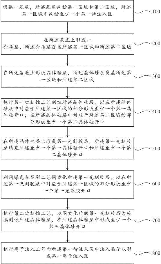
步骤100、提供一基底,所述基底包括第一区域和第二区域,所述第一区域中包括至少一个第一待注入区。
其中,图8为本发明实施例提供的一种基底的结构示意图。如图8所示,所述基底10包括第一区域C和第二区域D,其中,所述第一区域C可以为中压区域或者高压区域,所述第一区域C中可以包括至少一个第一待注入区C1,例如可以包括两个第一待注入区C1,所述两个第一待注入区C1可以分别用于形成源极和轻掺杂漏区(LDD区)。以及,所述第二区域D可以为低压区域,所述第二区域D中也可以包括至少一个第二待注入区D1,例如可以包括两个第二待注入区D1,所述两个第二待注入区D1可以分别用于形成源漏极。8 is a schematic structural diagram of a substrate provided by an embodiment of the present invention. As shown in FIG. 8 , the
本实施例中,所述第一区域C在平行于基底表面方向上的宽度尺寸远远大于所述第二区域D在平行于基底表面方向上的宽度尺寸,具体的,所述第一区域C在平行于基底表面方向上的宽度尺寸可以为所述第二区域D在平行于基底表面方向上的宽度尺寸的8~12倍(例如可以为10倍)。In this embodiment, the width dimension of the first region C in the direction parallel to the substrate surface is much larger than the width dimension of the second region D in the direction parallel to the substrate surface. Specifically, the first region C The width dimension in the direction parallel to the substrate surface may be 8 to 12 times (for example, 10 times) the width dimension of the second region D in the direction parallel to the substrate surface.
以及,本实施例中,所述第一待注入区C1和所述第二待注入区D1的截面的形状可以为矩形,且第一待注入区C1和所述第二待注入区D1在平行于基底10表面方向上的宽度尺寸可以相等。And, in this embodiment, the shape of the cross section of the first to-be-implanted region C1 and the second to-be-implanted region D1 may be rectangular, and the first to-be-implanted region C1 and the second to-be-implanted region D1 are parallel to each other. The width dimension in the direction of the surface of the
步骤200、在所述基底上形成一介质层,所述介质层覆盖所述第一区域C和所述第二区域D。
其中,参考图8所示,所述基底10上形成有覆盖所述第一区域C和所述第二区域D的介质层20,所述介质层20的材质例如可以为氧化硅或氮氧化硅,其可采用化学气相沉积(CVD)工艺形成。8 , a
步骤300、在所述基底上形成晶体硅层,所述晶体硅层覆盖所述第一区域和所述第二区域。
图9为本发明实施例提供的一种在图8所示的结构上形成了晶体硅层之后的半导体结构的示意图。如图9所示,所述基底10上形成有晶体硅层30,所述晶体硅层30覆盖所述第一区域C和所述第二区域D。其中,所述晶体硅层30的材质可以包括多晶硅,以及,可以采用外延生长的方法在所述介质层上生长出晶体硅层。FIG. 9 is a schematic diagram of a semiconductor structure after a crystalline silicon layer is formed on the structure shown in FIG. 8 according to an embodiment of the present invention. As shown in FIG. 9 , a
本实施例的方法尤其适合应用在晶体硅层的厚度较小的情况下,例如,当所述晶体硅层的厚度小于等于1500埃(例如为1000埃)时,采用本发明实施例所提供的半导体器件制造方法效果更佳。当然,即便所述晶体硅层的厚度大于1500埃时,也可以应用本实施例的方法。The method of this embodiment is especially suitable for application in the case where the thickness of the crystalline silicon layer is small. For example, when the thickness of the crystalline silicon layer is less than or equal to 1500 angstroms (for example, 1000 angstroms), the method provided by the embodiments of the present invention is adopted. The semiconductor device manufacturing method is more effective. Of course, even when the thickness of the crystalline silicon layer is greater than 1500 angstroms, the method of this embodiment can also be applied.
步骤400、执行第一次刻蚀工艺刻蚀所述晶体硅层,以在所述晶体硅层中对应于所述第一区域的部分形成至少一个第一晶体硅开口,在所述晶体硅层中对应于所述第二区域的部分形成至少一个第二晶体硅开口。Step 400: Perform a first etching process to etch the crystalline silicon layer, so as to form at least one first crystalline silicon opening in a portion of the crystalline silicon layer corresponding to the first region, and in the crystalline silicon layer At least one second crystalline silicon opening is formed in a portion corresponding to the second region.
其中,本实施例中,所述第一次刻蚀工艺的方法具体可以包括以下步骤:Wherein, in this embodiment, the method for the first etching process may specifically include the following steps:
第一步:在所述晶体硅层30上形成第二光刻胶层,所述第二光刻胶层覆盖所述第一区域C和所述第二区域D。The first step: forming a second photoresist layer on the
其中,图10为本发明实施例提供的一种在图9所示的结构上形成了第二光刻胶层之后的半导体结构的示意图。如图10所示,所述晶体硅层30上形成有第二光刻胶层40,所述第二光刻胶层40覆盖所述第一区域C和所述第二区域D。所述第二光刻胶层40例如是通过旋涂工艺形成。10 is a schematic diagram of a semiconductor structure after a second photoresist layer is formed on the structure shown in FIG. 9 according to an embodiment of the present invention. As shown in FIG. 10 , a
第二步:图案化所述第二光刻胶层40,以在所述第二光刻胶层40中对应于所述第一区域C的部分形成至少一个第二光刻胶开口,在所述第二光刻胶层40中对应于第二区域D的部分形成至少一个第三光刻胶开口。具体实施时,可通过曝光以及显影工艺图案化所述第二光刻胶层40。The second step: patterning the
其中,图11为本发明实施例提供的一种在图10所示的结构上形成了至少一个第二光刻胶开口和至少一个第三光刻胶开口之后的半导体结构的示意图(图中以形成两个第二光刻胶开口和两个第三光刻胶开口为例进行说明),图12为本发明实施例提供的图11的俯视图。11 is a schematic diagram of a semiconductor structure provided by an embodiment of the present invention after at least one second photoresist opening and at least one third photoresist opening are formed on the structure shown in FIG. The formation of two second photoresist openings and two third photoresist openings is described as an example), FIG. 12 is a top view of FIG. 11 according to an embodiment of the present invention.
如图11所示,在图案化所述晶体硅层30之后,所述图案化后的第二光刻胶层40中对应于第一区域C的部分形成有两个第二光刻胶开口41a,在对应于第二区域D的部分中形成有两个第三光刻胶开口41b。其中,参考图11,本实施例中的所述第二光刻胶开口41a和所述第三光刻胶开口41b的开口形状可以为矩形。As shown in FIG. 11 , after the
以及,需要说明的是,所述至少一个第二光刻胶开口41a和所述第一待注入区C1一一对应,具体可以包括为:第二光刻胶开口41a的数量与第一待注入区C1的数量相同,且每一个所述第二光刻胶开口41a在垂直于基底平面方向上的投影均对应落入至一个第一待注入区C1中,以及,所述第二光刻胶开口41a在平行于基底10表面方向的开口尺寸N(参考图11)小于对应的第一待注入区C1在平行于基底10表面方向的宽度尺寸M。And, it should be noted that the at least one
以及,所述第三光刻胶开口41b和所述第二待注入区D1一一对应,具体可以包括为:所述第三光刻胶开口41b的数量与所述第二待注入区D1的数量对应,且所述第三光刻胶开口41b的边沿与所述第二待注入区D1的边缘对齐,即:每一个所述第三光刻胶开口41b在垂直于基底平面方向上的投影均对应落入至一个第二待注入区D1中,且第三光刻胶开口41b在平行于基底10表面方向的开口尺寸等于第二待注入区D1在平行于基底10表面方向的宽度尺寸。And, the
第三步:以所述图案化后的第二光刻胶层40为掩膜刻蚀所述晶体硅层30,以形成至少一个第一晶体硅开口和至少一个第二晶体硅开口。例如可采用干法刻蚀工艺刻蚀所述晶体硅层30。The third step: etching the
其中,图13为本发明实施例提供的一种在图11所示的结构上形成了至少一个第一晶体硅开口和至少一个第二晶体硅开口之后的半导体结构的示意图。如图13所示,所述半导体结构中形成有至少一个第一晶体硅开口31a和至少一个第二晶体硅开口31b。其中,所述第一晶体硅开口31a与所述第二光刻胶开口41a相互连通,且所述第一晶体硅开口31a的开口形状与所述第二光刻胶开口41a的开口形状一致,可以均为矩形,以及,所述第一晶体硅开口31a的宽度尺寸与所述第二光刻胶开口41a的宽度尺寸也相等。以及,每个第一晶体硅开口31a在垂直于基底表面方向上的投影也均会对应落入至一个第一待注入区C1中,且所述第一晶体硅开口31a的开口尺寸小于对应的所述第一待注入区C1的宽度尺寸。13 is a schematic diagram of a semiconductor structure after at least one first crystalline silicon opening and at least one second crystalline silicon opening are formed on the structure shown in FIG. 11 according to an embodiment of the present invention. As shown in FIG. 13 , at least one first crystalline silicon opening 31 a and at least one second
所述第二晶体硅开口31b与所述第三光刻胶开口41b连通,所述第二晶体硅开口31b的开口形状与所述第三光刻胶开口41b的开口形状一致,可以均为矩形。以及,所述第二晶体硅开口31b与所述第二待注入区D1也一一对应,且所述第二晶体硅开口31b的边沿与所述第二待注入区D1的边缘对齐,具体包括为:第二晶体硅开口31b与所述第二待注入区D1的数量相等,每个第二晶体硅开口31b在垂直于基底表面方向上的投影均会对应落入至一个第二待注入区D1中,且所述第二晶体硅开口31b的开口尺寸等于对应的所述第二待注入区D1的宽度尺寸。The second
其中,需要说明的是,本实施例中,在执行第一次刻蚀工艺刻蚀所述晶体硅层30时,还会同步刻蚀介质层20中对应于所述第一晶体硅开口31a和所述第二晶体硅开口31b的部分,以暴露出所述基底10。It should be noted that, in this embodiment, when performing the first etching process to etch the
第四步:去除剩余的第二光刻胶层。例如,可采用氧气等离子体灰化工艺去除剩余的第二光刻胶层。Step 4: Remove the remaining second photoresist layer. For example, the remaining second photoresist layer may be removed using an oxygen plasma ashing process.
其中,图14为本发明实施例提供的一种在图13所示的结构中去除了剩余的第二光刻胶层之后的半导体结构的示意图。如图14所示,在去除了剩余的第二光刻胶层后,剩余的晶体硅层30在所述第一区域C中限定出了至少一个第一晶体硅开口31a,在所述第二区域D中限定出了至少一个第二晶体硅开口31b(图中均以两个为例进行说明)。其中,第一晶体硅开口31a暴露出部分所述第一待注入区C1。以及,所述第二晶体硅开口31b完全暴露出所述第二待注入区D1。14 is a schematic diagram of a semiconductor structure after removing the remaining second photoresist layer in the structure shown in FIG. 13 according to an embodiment of the present invention. As shown in FIG. 14, after the remaining second photoresist layer is removed, the remaining
此外,需要说明的是,本步骤中400中需要对晶体硅层30中对应于第二区域D的部分进行刻蚀,以形成完全暴露出所述第二待注入区D1的第二晶体硅开口31b。其中,鉴于所述第二区域D在平行于基底表面方向的宽度尺寸较小,则需要使得所述第二光刻胶层40的厚度较小,从而防止由于第二光刻胶层40的厚度较大,而导致在刻蚀第二区域D上的晶体硅层30时出现脱胶的现象。其中,第二光刻胶层40的厚度可以为所述基底10中第二区域D在平行于基底表面方向的宽度尺寸的3~5倍(例如可以为5倍),举例而言,若所述第二区域在平行于基底表面方向的宽度尺寸为60nm,所述第二光刻胶层40的厚度可以为300nm。In addition, it should be noted that in this
步骤500、在所述晶体硅层上形成第一光刻胶层,所述第一光刻胶层填充所述至少一个第一晶体硅开口和所述至少一个第二晶体硅开口。所述第一光刻胶层例如是通过旋涂工艺形成。Step 500: A first photoresist layer is formed on the crystalline silicon layer, and the first photoresist layer fills the at least one first crystalline silicon opening and the at least one second crystalline silicon opening. The first photoresist layer is formed by, for example, a spin coating process.
图15为本发明实施例提供的一种在图14所示的结构上形成第一光刻胶层之后的半导体结构的示意图,如图15所示,所述基底10上形成有第一光刻胶层50,所述第一光刻胶层50填充所述至少一个第一晶体硅开口31a和所述至少一个第二晶体硅开口31b。15 is a schematic diagram of a semiconductor structure after forming a first photoresist layer on the structure shown in FIG. 14 according to an embodiment of the present invention. As shown in FIG. 15 , a first photoresist layer is formed on the substrate 10
步骤600、利用曝光和显影工艺图案化所述第一光刻胶层50,以在所述第一光刻胶层50中对应于所述第一区域C的部分形成至少一个第一光刻胶开口,所述第一光刻胶开口与所述第一待注入区C1一一对应,且所述第一光刻胶开口的边沿与所述第一待注入区C1的边缘对齐。
其中,图16为本发明实施例提供的一种在图15所示的结构中形成至少一个第一光刻胶开口之后的半导体结构的示意图,如图16所示,在对所述第一光刻胶层50进行图案化后,图案化后的第一光刻胶层50在所述第一区域C中限定出至少一个第一光刻胶开口51(图中以两个第一光刻胶开口51为例进行说明),并且,所述第一光刻胶开口51与所述第一待注入区C1一一对应,且所述第一光刻胶开口51的边沿与所述第一待注入区C1的边缘对齐,具体包括为:所述第一光刻胶开口51与所述第一待注入区C1的数量相同,每个所述第一光刻胶开口51在垂直于所述基底表面方向上的投影均对应落入至一个第一待注入区C1中,且第一光刻胶开口51在平行于基底表面方向的开口尺寸与对应的所述第一待注入区C1在平行于基底表面方向的宽度尺寸相等。16 is a schematic diagram of a semiconductor structure after at least one first photoresist opening is formed in the structure shown in FIG. 15 according to an embodiment of the present invention, as shown in FIG. After the
步骤700、执行第二次刻蚀工艺,以图案化后的第一光刻胶层50为掩膜刻蚀所述晶体硅层30,在所述晶体硅层30中形成至少一个第三晶体硅开口。
图17为本发明实施例提供的一种在图16所示的结构中形成至少一个第三晶体硅开口之后的半导体结构的示意图,如图17所示,在以图案化后的第一光刻胶层50为掩膜刻蚀了所述晶体硅层30之后,在所述晶体硅层30中会形成至少一个第三晶体硅开口31c(图中以两个第三晶体硅开口31c为例进行说明)。其中,由于本实施例中,是以所述图案化后的第一光刻胶层50为掩膜刻蚀所述晶体硅层30的,则所述晶体硅层30在第二次刻蚀工艺中被刻蚀的部分应当为所述晶体硅层30中对应于所述第一光刻胶开口51的部分,基于此,形成在所述晶体硅层30中的第三晶体硅开口31c应当与所述第一光刻胶开口51是对齐的。FIG. 17 is a schematic diagram of a semiconductor structure after at least one third crystalline silicon opening is formed in the structure shown in FIG. 16 according to an embodiment of the present invention. As shown in FIG. 17 , after the patterned first photolithography After the
以及进一步地,本实施例中在以图案化后的第一光刻胶层50刻蚀所述晶体硅层30时,还会消耗掉部分第一光刻胶层50,则会使得第一光刻胶层50的厚度降低,其中,消耗掉的第一光刻胶层50的厚度与所要刻蚀的所述晶体硅层30的厚度比例关系为1:1。And further, in this embodiment, when the
但是,需要强调的是,本实施例中,应确保在执行完第二次刻蚀工艺之后,剩余的第二光刻胶层50的厚度较厚,例如大于等于0.3微米,从而使得最终剩余的第二光刻胶层50与剩余的晶体硅层30的总厚度较厚,例如大于等于0.4微米,以便后续在执行离子注入工艺,将剩余的第一光刻胶层和剩余的晶体硅层共同作为离子注入掩膜层时,可以确保离子注入掩膜层能够具备足够的厚度,防止出现离子击穿的现象。由此,本实施例中在步骤500中所形成的第一光刻胶层50的厚度应当较厚,应当至少大于晶体硅层30的厚度与0.3微米之和,例如步骤500中所形成的第一光刻胶层50的厚度可以为0.5微米。However, it should be emphasized that in this embodiment, it should be ensured that after the second etching process is performed, the thickness of the remaining
此外,需要说明的是,本步骤中在形成第三晶体硅开口31c之后,还会以所述图案化后的第一光刻胶层50为掩膜刻蚀所述介质层20以暴露出所述基底10。In addition, it should be noted that in this step, after the third
步骤800、执行离子注入工艺向所述第一待注入区中注入离子以形成第一离子注入区。
其中,由上述步骤600中的内容可知,最终所剩余的所述第一光刻胶层和剩余的所述晶体硅层是对齐的,且会完全暴露出第一待注入区C1,不会出现如相关技术中所出现的两者相互错开而使得部分晶体硅层未被第一光刻胶层覆盖而暴露在外界以及部分待注入区被第一光刻胶层覆盖的现象(例如可以对比图5和图17)。基于此,当执行离子注入工艺时,不会出现离子击穿暴露的晶体硅层而误注入至非待注入区或者由于第一光刻胶层的阻挡而使得离子无法注入至第一待注入区的现象发生,则可以确保离子能够被准确的注入至第一待注入区C1,从而可以形成准确的离子注入形貌,并且,基于剩余的第一光刻胶层和剩余的所述晶体硅层具备足够的厚度,则在执行离子注入工艺时同样可以防止离子击穿离子注入掩膜层这一现象的发生,可以进一步确保形成准确且理想的离子注入形貌。Wherein, it can be known from the content in the
其中,图18为本发明实施例提供的一种对图17所示的结构执行了离子注入工艺之后的半导体结构的示意图,对比图6和图18所示,采用本实施例所提供的半导体的制造方法所制造的半导体结构中,离子能够被准确的注入至第一待注入区C1中,形成形貌准确的第一离子注入区C2。18 is a schematic diagram of a semiconductor structure after an ion implantation process is performed on the structure shown in FIG. 17 according to an embodiment of the present invention. Compared with FIG. 6 and FIG. In the semiconductor structure manufactured by the manufacturing method, ions can be accurately implanted into the first to-be-implanted region C1 to form the first ion-implanted region C2 with accurate topography.
在本实施例中,执行完步骤700之后,所述方法还可以包括:去除剩余的第一光刻胶层,以进行后续步骤。In this embodiment, after
以及,需要说明的是,本实施例中的半导体器件的制造方法主要用于制造包括有LDD区的半导体器件(例如可以为液晶驱动器)。And, it should be noted that the manufacturing method of the semiconductor device in this embodiment is mainly used to manufacture a semiconductor device including an LDD region (for example, a liquid crystal driver).
综上所述,采用本发明提供的半导体器件制造方法,可以形成形貌准确的离子注入区,从而确保了最终制成的半导体器件的电性能和良率。To sum up, by using the semiconductor device manufacturing method provided by the present invention, an ion implantation region with accurate topography can be formed, thereby ensuring the electrical performance and yield of the finally fabricated semiconductor device.
以及,需要说明的是,本发明中在刻蚀形成所述至少一个第一晶体硅开口的时,还会同步刻蚀所述晶体硅层中对应于第二区域的部分,以在晶体硅层中对应于第二区域的部分形成至少一个第二晶体硅开口,所述第二晶体硅开口会暴露出所述第二区域的第二待注入区,以便后续对所述第二待注入区进行离子注入。由此,本发明还可以节省工艺步骤,简化工艺流程,提高效率。And, it should be noted that, in the present invention, when the at least one first crystalline silicon opening is formed by etching, the part corresponding to the second region in the crystalline silicon layer is also etched synchronously, so that the crystalline silicon layer is etched simultaneously. At least one second crystalline silicon opening is formed in the part corresponding to the second region, and the second crystalline silicon opening will expose the second to-be-implanted region of the second region, so that the second to-be-implanted region can be subsequently implanted. Ion Implantation. Therefore, the present invention can also save process steps, simplify the process flow, and improve efficiency.
本说明书中各个实施例采用递进的方式描述,每个实施例重点说明的都是与其他实施例的不同之处,各个实施例之间相同相似部分互相参见即可。对于实施例公开的系统而言,由于与实施例公开的方法相对应,所以描述的比较简单,相关之处参见方法部分说明即可。The various embodiments in this specification are described in a progressive manner, and each embodiment focuses on the differences from other embodiments, and the same and similar parts between the various embodiments can be referred to each other. For the system disclosed in the embodiment, since it corresponds to the method disclosed in the embodiment, the description is relatively simple, and the relevant part can be referred to the description of the method.
上述描述仅是对本发明较佳实施例的描述,并非对本发明范围的任何限定,本发明领域的普通技术人员根据上述揭示内容做的任何变更、修饰,均属于权利要求书的保护范围。The above description is only a description of the preferred embodiments of the present invention, and is not intended to limit the scope of the present invention. Any changes and modifications made by those of ordinary skill in the field of the present invention based on the above disclosure all belong to the protection scope of the claims.
Claims (11)
Priority Applications (1)
| Application Number | Priority Date | Filing Date | Title |
|---|---|---|---|
| CN202010938519.XA CN111933521B (en) | 2020-09-09 | 2020-09-09 | Method for manufacturing semiconductor device |
Applications Claiming Priority (1)
| Application Number | Priority Date | Filing Date | Title |
|---|---|---|---|
| CN202010938519.XA CN111933521B (en) | 2020-09-09 | 2020-09-09 | Method for manufacturing semiconductor device |
Publications (2)
| Publication Number | Publication Date |
|---|---|
| CN111933521A true CN111933521A (en) | 2020-11-13 |
| CN111933521B CN111933521B (en) | 2021-01-01 |
Family
ID=73309880
Family Applications (1)
| Application Number | Title | Priority Date | Filing Date |
|---|---|---|---|
| CN202010938519.XA Active CN111933521B (en) | 2020-09-09 | 2020-09-09 | Method for manufacturing semiconductor device |
Country Status (1)
| Country | Link |
|---|---|
| CN (1) | CN111933521B (en) |
Citations (5)
| Publication number | Priority date | Publication date | Assignee | Title |
|---|---|---|---|---|
| CN101064280A (en) * | 2006-04-28 | 2007-10-31 | 富士通株式会社 | Method of manufacturing semiconductor device |
| JP2014096465A (en) * | 2012-11-09 | 2014-05-22 | Fuji Electric Co Ltd | Silicon carbide mos semiconductor device manufacturing method |
| CN104167391A (en) * | 2014-08-11 | 2014-11-26 | 矽力杰半导体技术(杭州)有限公司 | Method for manufacturing CMOS structure |
| CN104867829A (en) * | 2014-02-20 | 2015-08-26 | 北大方正集团有限公司 | Metal-oxide semiconductor device manufacturing method and metal-oxide semiconductor device |
| CN108878275A (en) * | 2017-05-10 | 2018-11-23 | 中芯国际集成电路制造(上海)有限公司 | The preparation method of semiconductor devices |
-
2020
- 2020-09-09 CN CN202010938519.XA patent/CN111933521B/en active Active
Patent Citations (5)
| Publication number | Priority date | Publication date | Assignee | Title |
|---|---|---|---|---|
| CN101064280A (en) * | 2006-04-28 | 2007-10-31 | 富士通株式会社 | Method of manufacturing semiconductor device |
| JP2014096465A (en) * | 2012-11-09 | 2014-05-22 | Fuji Electric Co Ltd | Silicon carbide mos semiconductor device manufacturing method |
| CN104867829A (en) * | 2014-02-20 | 2015-08-26 | 北大方正集团有限公司 | Metal-oxide semiconductor device manufacturing method and metal-oxide semiconductor device |
| CN104167391A (en) * | 2014-08-11 | 2014-11-26 | 矽力杰半导体技术(杭州)有限公司 | Method for manufacturing CMOS structure |
| CN108878275A (en) * | 2017-05-10 | 2018-11-23 | 中芯国际集成电路制造(上海)有限公司 | The preparation method of semiconductor devices |
Also Published As
| Publication number | Publication date |
|---|---|
| CN111933521B (en) | 2021-01-01 |
Similar Documents
| Publication | Publication Date | Title |
|---|---|---|
| CN101114571B (en) | Semiconductor device | |
| JP4046436B2 (en) | Contact formation method for semiconductor device | |
| US20090325106A1 (en) | Method for Implant Imaging with Spin-on Hard Masks | |
| KR100853796B1 (en) | Manufacturing Method of Semiconductor Device | |
| US7485523B2 (en) | Method for forming high voltage device and semiconductor device | |
| CN111933521A (en) | Method for manufacturing semiconductor device | |
| CN114420629A (en) | Semiconductor structure and manufacturing method thereof | |
| KR100753105B1 (en) | Method of manufacturing recess pattern of semiconductor device | |
| JP2003008017A (en) | Method for manufacturing semiconductor device | |
| KR100909162B1 (en) | Method of manufacturing semiconductor device | |
| JP2754202B2 (en) | Method for manufacturing semiconductor device | |
| KR100588779B1 (en) | Semiconductor device and manufacturing method | |
| KR0161727B1 (en) | Element isolation method of semiconductor device | |
| KR20030094940A (en) | Method of manufacturing a semiconductor device | |
| KR100778877B1 (en) | Manufacturing method of semiconductor device | |
| KR100677992B1 (en) | Manufacturing Method of Semiconductor Device | |
| KR100466025B1 (en) | Method manufacturing semiconductor device having sti structure | |
| KR100246784B1 (en) | Manufacturing Method of Flash Memory Cell | |
| KR100773242B1 (en) | Manufacturing Method of Semiconductor Device | |
| KR100298462B1 (en) | Method for Manufacturing of Semiconductor Device | |
| KR100770534B1 (en) | Manufacturing Method of Semiconductor Device | |
| KR100621451B1 (en) | Manufacturing Method of Semiconductor Device | |
| CN112701080A (en) | Through hole forming method | |
| KR20070036295A (en) | Manufacturing method of semiconductor device | |
| JPH04107819A (en) | Manufacture of semiconductor device |
Legal Events
| Date | Code | Title | Description |
|---|---|---|---|
| PB01 | Publication | ||
| PB01 | Publication | ||
| SE01 | Entry into force of request for substantive examination | ||
| SE01 | Entry into force of request for substantive examination | ||
| GR01 | Patent grant | ||
| GR01 | Patent grant | ||
| TR01 | Transfer of patent right | ||
| TR01 | Transfer of patent right |
Effective date of registration: 20240321 Address after: 230012 No.88, xifeihe Road, Hefei comprehensive free trade zone, Xinzhan District, Hefei City, Anhui Province Patentee after: Nexchip Semiconductor Corporation Country or region after: China Address before: No.18-h1105, Yinchun Road, science and technology R & D base, Maigaoqiao entrepreneurship Park, Qixia District, Nanjing, Jiangsu Province, 210046 Patentee before: Nanjing crystal drive integrated circuit Co.,Ltd. Country or region before: China |