CN111668190B - Hot electron effect characterization method based on compound material MISFET device - Google Patents
Hot electron effect characterization method based on compound material MISFET device Download PDFInfo
- Publication number
- CN111668190B CN111668190B CN201910173484.2A CN201910173484A CN111668190B CN 111668190 B CN111668190 B CN 111668190B CN 201910173484 A CN201910173484 A CN 201910173484A CN 111668190 B CN111668190 B CN 111668190B
- Authority
- CN
- China
- Prior art keywords
- voltage
- characteristic
- hot electron
- stress
- electrode
- Prior art date
- Legal status (The legal status is an assumption and is not a legal conclusion. Google has not performed a legal analysis and makes no representation as to the accuracy of the status listed.)
- Active
Links
Images


Classifications
-
- H10P74/277—
-
- G—PHYSICS
- G01—MEASURING; TESTING
- G01R—MEASURING ELECTRIC VARIABLES; MEASURING MAGNETIC VARIABLES
- G01R31/00—Arrangements for testing electric properties; Arrangements for locating electric faults; Arrangements for electrical testing characterised by what is being tested not provided for elsewhere
- G01R31/26—Testing of individual semiconductor devices
- G01R31/2601—Apparatus or methods therefor
-
- G—PHYSICS
- G01—MEASURING; TESTING
- G01R—MEASURING ELECTRIC VARIABLES; MEASURING MAGNETIC VARIABLES
- G01R31/00—Arrangements for testing electric properties; Arrangements for locating electric faults; Arrangements for electrical testing characterised by what is being tested not provided for elsewhere
- G01R31/26—Testing of individual semiconductor devices
- G01R31/2642—Testing semiconductor operation lifetime or reliability, e.g. by accelerated life tests
Landscapes
- Physics & Mathematics (AREA)
- General Physics & Mathematics (AREA)
- Testing Or Measuring Of Semiconductors Or The Like (AREA)
Abstract
本发明涉及一种基于MISFET器件热电子效应的测试结构,包括:衬底(1)、P型外延层(2)、绝缘层(3)、钝化层(4)、栅极(5)、第一N+掺杂区(6)、源极(7)、漏极(8)、P+掺杂区(9)、第二N+掺杂区(10)、电极A(11)和电极B(12)。本实施例提供了一种热电子注入数量与能量可控技术的异质结器件测试结构和热电子效应表征方法,通过调整电压Va和Vb来控制绝缘层中热电子的注入数量,并通过调整电压Va来控制绝缘层中热电子的注入能量,解决了器件热电子注入数量和注入能量的不可控,以及非均匀注入绝缘层等问题,有助于对异质结器件中的热电子效应进行深入分析。
The invention relates to a test structure based on thermionic effect of MISFET devices, comprising: a substrate (1), a P-type epitaxial layer (2), an insulating layer (3), a passivation layer (4), a gate (5), First N+ doped region (6), source (7), drain (8), P+ doped region (9), second N+ doped region (10), electrode A (11) and electrode B (12) ). This embodiment provides a test structure of a heterojunction device and a method for characterizing thermionic effect of a technology with controllable hot electron injection quantity and energy. The injection quantity of hot electrons in the insulating layer is controlled by adjusting the voltages Va and Vb. The voltage Va is used to control the injection energy of hot electrons in the insulating layer, which solves the problems of uncontrollable number and injection energy of hot electrons injected into the device, as well as non-uniform injection into the insulating layer, etc. In-depth analysis.
Description
技术领域technical field
本发明属于微电子可靠性表征技术领域,具体涉及一种基于化合物材料MISFET器件的热电子效应表征方法。The invention belongs to the technical field of microelectronic reliability characterization, and in particular relates to a method for characterizing thermionic effect of a compound material MISFET device.
背景技术Background technique
从以硅材料为代表的第一代半导体材料到以砷化镓材料为代表的第二代半导体材料,发展到以氮化镓为代表的第三代半导体材料,材料特性愈发优异,为更高性能半导体器件乃至集成电路提供了坚实的材料基础。尤其是第三代宽禁带半导体材料具有击穿场强高、热导率大、电子饱和漂移速度高等优良特点,基于其制作而成的半导体器件在大功率、高频率、高电压、高温和耐辐射等领域具有独特优势。From the first-generation semiconductor materials represented by silicon materials to the second-generation semiconductor materials represented by gallium arsenide materials, to the third-generation semiconductor materials represented by gallium nitride, the material properties are getting better and better. High-performance semiconductor devices and even integrated circuits provide a solid material foundation. In particular, the third-generation wide-bandgap semiconductor materials have the characteristics of high breakdown field strength, high thermal conductivity, and high electron saturation drift speed. Radiation resistance and other fields have unique advantages.
在实际应用中,金属-绝缘体-半导体场效应晶体管(MISFET,Metal InsulationSemiconductor Field Effect Transistor)在高压条件下工作时,其沟道中的电子在强电场加速作用下获得足够高的能量变成高能“热电子”。这些高能热电子会跃出导电沟道,注入到绝缘层材料中,导致器件性能发生退化,即热电子效应。目前,对于MISFET器件热电子效应的表征研究,一般采用对常规结构的MISFET施加热电子应力偏置,分析应力前后器件特性变化的方法。In practical applications, when a metal-insulator-semiconductor field effect transistor (MISFET) works under high voltage conditions, the electrons in its channel are accelerated by a strong electric field to obtain a sufficiently high energy to become high-energy "heat". electronic". These high-energy hot electrons will jump out of the conductive channel and be injected into the insulating layer material, resulting in the degradation of device performance, that is, the hot electron effect. At present, for the characterization research of thermionic effect of MISFET devices, the method of applying thermionic stress bias to the MISFET of conventional structure and analyzing the change of device characteristics before and after stress is generally adopted.
然而,针对常规结构的n沟道MISFET器件施加热电子应力时,由于从漏极到源极存在电势差,使得热电子在沟道内的分布并不均匀,而且沟道内载流子的数量和其加速电场强度均与所加栅源电压、栅漏电压偏置均同时相关。因此,仅对常规结构n沟道MISFET器件施加热电子应力时,不能实现对绝缘层均匀地注入热电子,也无法独立研究热电子注入数量和注入能量分别对器件性能退化的影响,从而对于热电子效应的机理缺乏深入的研究与表征。However, when the hot electron stress is applied to the n-channel MISFET device with a conventional structure, due to the potential difference from the drain to the source, the distribution of hot electrons in the channel is not uniform, and the number of carriers in the channel and its acceleration are not uniform. The electric field strength is related to the applied gate-source voltage and gate-drain voltage bias simultaneously. Therefore, when only applying hot electron stress to the conventional n-channel MISFET device, it is not possible to inject hot electrons uniformly into the insulating layer, and it is also impossible to independently study the effects of hot electron injection quantity and injection energy on the performance degradation of the device. The mechanism of electronic effect lacks in-depth research and characterization.
发明内容SUMMARY OF THE INVENTION
为了解决现有技术中存在的上述问题,本发明提供了一种基于化合物材料MISFET器件的热电子效应表征方法。本发明要解决的技术问题通过以下技术方案实现:In order to solve the above problems existing in the prior art, the present invention provides a method for characterizing thermionic effect of a compound material MISFET device. The technical problem to be solved by the present invention is realized by the following technical solutions:
本发明实施例提供了一种基于化合物材料MISFET器件的热电子效应测试结构,包括:衬底、P型外延层、绝缘层、钝化层、栅极、第一N+掺杂区、源极、漏极、P+掺杂区、第二N+掺杂区、电极A和电极B;其中,An embodiment of the present invention provides a thermionic effect test structure based on a compound material MISFET device, including: a substrate, a P-type epitaxial layer, an insulating layer, a passivation layer, a gate, a first N+ doped region, a source, drain, P+ doped region, second N+ doped region, electrode A and electrode B; wherein,
所述P型外延层位于所述衬底之上;the P-type epitaxial layer is located on the substrate;
所述绝缘层位于所述P型外延层之上;the insulating layer is located on the P-type epitaxial layer;
所述栅极位于所述绝缘层之上;the gate is located on the insulating layer;
两个所述第一N+掺杂区对应分布在所述P型外延层内;The two first N+ doped regions are correspondingly distributed in the P-type epitaxial layer;
所述源极和所述漏极分别位于两个所述第一N+掺杂区之上;the source electrode and the drain electrode are respectively located on the two first N+ doped regions;
所述P+掺杂区和所述第二N+掺杂区位于所述P型外延层内;其中,所述P+掺杂区分布在对应的所述第一N+掺杂区外侧,所述第二N+掺杂区分布在对应的所述P+掺杂区外侧;The P+ doping region and the second N+ doping region are located in the P-type epitaxial layer; wherein, the P+ doping region is distributed outside the corresponding first N+ doping region, and the second N+ doped regions are distributed outside the corresponding P+ doped regions;
所述电极A位于所述P+掺杂区之上;the electrode A is located above the P+ doped region;
所述电极B位于所述第二N+掺杂区之上;the electrode B is located above the second N+ doped region;
所述钝化层位于所述P型外延层之上,且所述钝化层位于所述绝缘层、所述源极、所述漏极、所述电极A和所述电极B四周。The passivation layer is located on the P-type epitaxial layer, and the passivation layer is located around the insulating layer, the source electrode, the drain electrode, the electrode A and the electrode B.
本发明的另一个实施例提供了一种基于化合物材料MISFET器件的热电子效应表征方法,应用于一种基于化合物材料MISFET器件的热电子效应测试结构,以对待测器件的热电子效应进行表征,该方法包括:Another embodiment of the present invention provides a method for characterizing thermionic effect of a compound material MISFET device, which is applied to a thermionic effect test structure based on a compound material MISFET device to characterize the thermionic effect of the device under test, The method includes:
通过热电子应力实验获取所述待测器件的第一特性和第二特性;Obtain the first characteristic and the second characteristic of the device under test through a hot electron stress experiment;
根据所述第一特性和所述第二特性,获取所述热电子应力实验对所述待测器件特性影响的结果;其中,所述热电子应力实验对所述待测器件特性影响的结果,包括获取热电子注入数量对所述待测器件特性影响的结果、热电子注入能量对所述待测器件特性影响的结果和栅极电压对热电子效应影响的结果。According to the first characteristic and the second characteristic, the result of the influence of the hot electron stress experiment on the characteristics of the device under test is obtained; wherein, the result of the influence of the hot electron stress experiment on the characteristics of the device under test, The method includes obtaining the result of the influence of the amount of hot electron injection on the characteristics of the device under test, the result of the influence of the hot electron injection energy on the characteristics of the device to be tested, and the result of the influence of the gate voltage on the hot electron effect.
在本发明的一个实施例中,所述第一特性和所述第二特性均包括:输出特性和转移特性。In an embodiment of the present invention, both the first characteristic and the second characteristic include: an output characteristic and a transfer characteristic.
在本发明的一个实施例中,通过热电子应力实验获取所述待测器件的第一特性和第二特性,包括:In an embodiment of the present invention, the first characteristic and the second characteristic of the device under test are obtained through a hot electron stress experiment, including:
获取所述待测器件的第一特性;obtaining the first characteristic of the device under test;
对所述电极A施加第一电压,对所述电极B施加第二电压,对所述栅极施加第三电压,并获取应力时间和栅极电流;其中,所述栅极电流为流过所述栅极的电流;A first voltage is applied to the electrode A, a second voltage is applied to the electrode B, and a third voltage is applied to the gate, and the stress time and gate current are obtained; the current of the gate;
撤去所述第一电压、所述第二电压和所述第三电压后,获取所述第二特性。After removing the first voltage, the second voltage and the third voltage, the second characteristic is obtained.
在本发明的一个实施例中,所述第一电压和所述第二电压满足以下公式:In an embodiment of the present invention, the first voltage and the second voltage satisfy the following formula:
Va-Vb>Von,Va-Vb>Von,
其中,所述Va为所述第一电压,所述Vb为所述第二电压,所述Von为所述P型外延层与所述第二N+掺杂区形成pn结的导通电压。Wherein, the Va is the first voltage, the Vb is the second voltage, and the Von is the turn-on voltage at which the P-type epitaxial layer and the second N+ doped region form a pn junction.
在本发明的一个实施例中,获取热电子注入数量对所述待测器件特性影响的结果,包括:In an embodiment of the present invention, obtaining a result of the influence of the number of hot electron injections on the characteristics of the device under test includes:
保持所述第一电压恒定不变,多次改变所述第二电压进行所述应力试验,并获取多组第一应力实验数据;其中,第一应力实验数据包括所述第一特性、所述第二特性、所述应力时间、所述栅极电流;Keeping the first voltage constant, changing the second voltage multiple times to perform the stress test, and acquiring multiple sets of first stress test data; wherein the first stress test data includes the first characteristic, the a second characteristic, the stress time, the gate current;
根据多组所述第一应力实验数据获取注入电子数量对所述待测器件特性影响的结果。The results of the influence of the quantity of injected electrons on the characteristics of the device under test are obtained according to the plurality of sets of experimental data of the first stress.
在本发明的一个实施例中,获取热电子注入能量对所述待测器件特性影响的结果,包括:In an embodiment of the present invention, obtaining the result of the influence of the hot electron injection energy on the characteristics of the device under test includes:
保持所述第一电压和所述第二电压的压差恒定,多次改变所述第一电压和所述第二电压进行所述应力试验,并获取多组第二应力实验数据,其中,每组第二应力实验数据包括所述第一特性、所述第二特性、所述应力时间和所述栅极电流;Keep the voltage difference between the first voltage and the second voltage constant, change the first voltage and the second voltage multiple times to carry out the stress test, and obtain multiple sets of second stress test data, wherein each a second set of stress experimental data including the first characteristic, the second characteristic, the stress time and the gate current;
根据多组所述第二应力实验数据获取注入电子能量对所述待测器件特性影响的结果。The results of the influence of the injected electron energy on the characteristics of the device under test are obtained according to the plurality of sets of the second stress experimental data.
在本发明的一个实施例中,获取栅极电压对热电子效应的影响的结果,包括:In one embodiment of the present invention, obtaining the results of the influence of the gate voltage on the thermionic effect includes:
保持所述第一电压和所述第二电压恒定不变;多次改变所述第三电压进行所述应力试验,并获取多组第三应力实验数据;其中,每组第三应力实验数据包括所述第一特性、所述第二特性、所述应力时间和所述栅极电流;Keep the first voltage and the second voltage constant; change the third voltage multiple times to carry out the stress test, and obtain multiple sets of third stress experimental data; wherein, each set of third stress experimental data includes the first characteristic, the second characteristic, the stress time, and the gate current;
根据多组所述第三应力实验数据获取栅极电压对热电子效应的影响的结果。The results of the effect of the gate voltage on the hot electron effect are obtained according to the plurality of sets of the third stress experiment data.
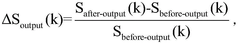
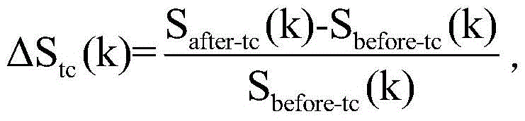
在本发明的一个实施例中,获取所述热电子应力实验对所述待测器件特性的影响的结果,包括:获取输出特性的相对退化量和转移特性的相对退化量。In an embodiment of the present invention, acquiring the result of the influence of the hot electron stress experiment on the characteristics of the device under test includes: acquiring the relative degradation amount of the output characteristic and the relative degradation amount of the transfer characteristic.
在本发明的一个实施例中,所述输出特性的相对退化量满足以下公式:In an embodiment of the present invention, the relative degradation amount of the output characteristic satisfies the following formula:

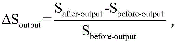
所述转移特性的相对退化量满足以下公式:The relative degradation amount of the transfer characteristic satisfies the following formula:
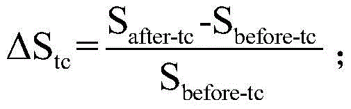
其中,ΔSoutput为所述输出特性的相对退化量,Safter-output为所述第二特性中的所述输出特性,Sbefore-output为所述第一特性中的所述输出特性,ΔStc为所述转移特性的相对退化量,Safter-tc为所述第二特性中的所述转移特性,Sbefore-tc为所述第一特性中的所述转移特性。Wherein, ΔS output is the relative degradation amount of the output characteristic, S after-output is the output characteristic in the second characteristic, S before-output is the output characteristic in the first characteristic, ΔS tc is the relative degradation amount of the transfer characteristic, S after-tc is the transfer characteristic in the second characteristic, and S before-tc is the transfer characteristic in the first characteristic.
与现有技术相比,本发明的有益效果:Compared with the prior art, the beneficial effects of the present invention:
1)本发明与传统热电子表征相比,其注入绝缘层中的热电子来源于第二N+掺杂区注入到外延层的电子,该电子数量由P/N+结上的偏压(Va-Vb)决定。因此,可调整偏置电压(Va-Vb)来控制绝缘层中热电子的注入数量;1) Compared with the traditional hot electron characterization of the present invention, the hot electrons injected into the insulating layer originate from the electrons injected into the epitaxial layer from the second N+ doped region, and the number of electrons is determined by the bias voltage (Va-) on the P/N+ junction. Vb) decision. Therefore, the bias voltage (Va-Vb) can be adjusted to control the injection quantity of hot electrons in the insulating layer;
2)本发明与传统热电子表征相比,其注入绝缘层中热电子的能量由P+掺杂区与沟道区之间的加速电场决定。由于源极S、漏极D极均接地,整个沟道区可视为0V等势区,则热电子的加速电场由Va决定。因此,可通过调整偏置电压Va来控制绝缘层中热电子的注入能量;2) Compared with the traditional hot electron characterization, the energy of the hot electron injected into the insulating layer is determined by the accelerating electric field between the P+ doped region and the channel region. Since both the source S and the drain D are grounded, the entire channel region can be regarded as a 0V equipotential region, and the accelerating electric field of hot electrons is determined by Va. Therefore, the injection energy of hot electrons in the insulating layer can be controlled by adjusting the bias voltage Va ;
3)本发明中,外延层电子在P+掺杂区与沟道区之间电场的加速作用下,部分成为热电子。由于源极S、漏极D接地,整个沟道区可视为0V等势区,靠近沟道下方的电场可视为匀强电场,且方向垂直沟道向下,故热电子会均匀地向器件绝缘层注入,有助于深入研究热电子效应;3) In the present invention, part of the electrons in the epitaxial layer become hot electrons under the acceleration of the electric field between the P+ doped region and the channel region. Since the source S and the drain D are grounded, the entire channel region can be regarded as a 0V equipotential region, and the electric field near the channel can be regarded as a uniform electric field, and the direction is vertical to the channel downward, so the hot electrons will be evenly distributed to the channel. Implantation of device insulating layer, which is helpful for in-depth study of hot electron effect;
4)本发明中,该器件在热电子应力实验过程中,源极和漏极接地,整个沟道区可视为0V等势区,而且栅极电压Vg>0,会在整个绝缘层中形成均匀的纵向电场,且方向为从栅极指向沟道。该纵向电场会促进热电子向绝缘层中注入,阻止外延层中的空穴向绝缘层注入。因此,热电子应力后,绝缘层的损伤仅由热电子注入引起,与空穴无关。4) In the present invention, during the hot electron stress experiment, the source and drain of the device are grounded, the entire channel region can be regarded as a 0V equipotential region, and the gate voltage Vg>0 will form in the entire insulating layer. Uniform longitudinal electric field, and the direction is from the gate to the channel. The longitudinal electric field promotes the injection of hot electrons into the insulating layer, and prevents the injection of holes in the epitaxial layer into the insulating layer. Therefore, after hot electron stress, the damage of the insulating layer is only caused by hot electron injection, and has nothing to do with holes.
附图说明Description of drawings
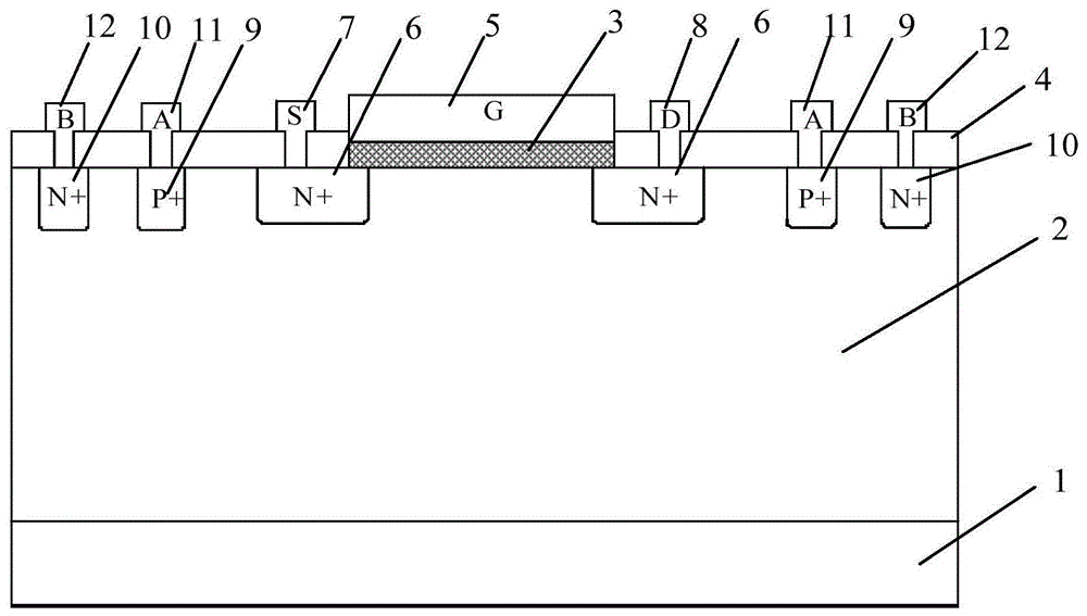
图1为本发明提供的一种基于化合物材料MISFET器件的热电子效应测试结构的结构示意图;1 is a schematic structural diagram of a thermionic effect test structure based on a compound material MISFET device provided by the present invention;
图2为本发明提供的一种基于化合物材料MISFET器件的结构示意图;2 is a schematic structural diagram of a compound material-based MISFET device provided by the present invention;
图3为本发明提供的一种基于化合物材料MISFET器件的热电子效应表征方法的流程示意图;3 is a schematic flowchart of a method for characterizing thermionic effect of a compound material MISFET device provided by the present invention;
图4为本发明提供的一种基于化合物材料MISFET器件的热电子效应表征方法的电路连接示意图;4 is a schematic diagram of circuit connection of a method for characterizing thermionic effect of a compound material MISFET device provided by the present invention;
图5为本发明提供的一种基于化合物材料MISFET器件的热电子效应表征方法的实现流程图;Fig. 5 is the realization flow chart of a kind of thermionic effect characterization method based on compound material MISFET device provided by the present invention;
图6a-6b为本发明提供待测器件输出特性与转移特性的退化量分别随不同热电子注入数量变化的曲线图;Figures 6a-6b are graphs showing the variation of the degradation amount of the output characteristic and the transfer characteristic of the device under test with different hot electron injection quantities according to the present invention;
图7a-7b为本发明提供待测器件输出特性与转移特性的退化量分别随不同热电子注入能量变化的曲线图;7a-7b are graphs showing the variation of the output characteristics and transfer characteristics of the device under test with different hot electron injection energies, respectively, according to the present invention;
图8a-8b为本发明提供待测器件输出特性与转移特性的退化量分别随不同栅极电压变化的曲线图。8a-8b are graphs showing the variation of the output characteristics and transfer characteristics of the device under test with different gate voltages, respectively, according to the present invention.
具体实施方式Detailed ways
下面结合具体实施例对本发明做进一步详细的描述,但本发明的实施方式不限于此。The present invention will be described in further detail below with reference to specific embodiments, but the embodiments of the present invention are not limited thereto.
实施例一:Example 1:
请参见图1和图2,图1为本发明提供的一种基于化合物材料MISFET器件的热电子效应测试结构的结构示意图;图2为本发明提供的一种基于化合物材料MISFET器件的结构示意图。本实施例以一种基于化合物材料MISFET器件为例,如图1所示。一种基于化合物材料MISFET器件的热电子效应测试结构,包括:衬底1、P型外延层2、绝缘层3、钝化层4、栅极5、第一N+掺杂区6、源极7、漏极8、P+掺杂区9、第二N+掺杂区10、电极A11和电极B12;其中,Please refer to FIG. 1 and FIG. 2. FIG. 1 is a schematic structural diagram of a thermal electron effect test structure based on a compound material MISFET device provided by the present invention; FIG. 2 is a structural schematic diagram of a compound material based MISFET device provided by the present invention. This embodiment takes a compound material-based MISFET device as an example, as shown in FIG. 1 . A thermionic effect test structure based on a compound material MISFET device, comprising: a substrate 1, a P-
所述P型外延层2位于所述衬底1之上;The P-
所述绝缘层3位于所述P型外延层2之上;The insulating layer 3 is located on the P-
所述栅极5位于所述绝缘层3之上;the
两个所述第一N+掺杂区6对应分布在所述P型外延层2内;The two first N+ doped
所述源极7和所述漏极8分别位于两个所述第一N+掺杂区6之上;The source electrode 7 and the drain electrode 8 are respectively located on the two first N+ doped
所述P+掺杂区9和所述第二N+掺杂区10位于所述P型外延层2内;其中,所述P+掺杂区9分布在对应的所述第一N+掺杂区6外侧,所述第二N+掺杂区10分布在对应的所述P+掺杂区9外侧;The P+ doped
所述电极A11位于所述P+掺杂区9之上;The electrode A11 is located above the P+ doped
所述电极B12位于所述第二N+掺杂区10之上;the electrode B12 is located on the second N+ doped
所述钝化层4位于所述P型外延层2之上,且所述钝化层4位于所述绝缘层3、所述源极7、所述漏极8、所述电极A11和所述电极B12四周。The passivation layer 4 is located on the P-
优选的,所述P型外延层2为P型掺杂外延层,所述第一N+掺杂区6为N+重掺杂区,所述P+掺杂区9为P+重掺杂区,所述第二N+掺杂区10为N+重掺杂区。Preferably, the P-
优选地,制作该器件时,首先选取基于化合物材料MISFET器件,如图2所示,包括:衬底21,P型外延层22、绝缘层23、钝化层24、栅极25、N+掺杂区26、源极27和漏极28;其中,P型外延层22位于衬底21之上,绝缘层23位于P型外延层22之上,钝化层24位于绝缘层23两侧,栅极25位于绝缘层23之上,两个N+掺杂区26对应分布在P型外延层22内,源极27和漏极28穿透钝化层24,且源极27和漏极28分别位于N+掺杂区26之上。Preferably, when making the device, first select a MISFET device based on compound materials, as shown in FIG. 2, including:
优选地,对该MISFET器件的源极27和漏极28两侧的绝缘层23分别进行刻蚀,刻蚀深度与绝缘层23厚度相同,即保留源极27与漏极28之间的P型外延层22,将源极27与漏极28两侧的绝缘层23刻蚀掉,暴露出P型外延层22。接着在源极27和漏极28两侧的P型外延层22表面,由内向外分别制作对称的P+、N+重掺杂区域,并分别在P+、N+重掺杂区域上制作欧姆电极A、B,完成基于MISFET器件的测试结构制备。Preferably, the insulating
本发明提供的一种基于化合物材料MISFET器件的热电子效应测试结构的结构,该测试结构针对沟道区域可提供均匀的热电子注入源,有助于对异质结器件中的热电子效应进行深入分析。The invention provides a structure of a thermionic effect test structure based on a compound material MISFET device, the test structure can provide a uniform hot electron injection source for the channel region, which is helpful for the detection of the thermionic effect in the heterojunction device. In-depth analysis.
实施例二:Embodiment 2:
请继续参见图1,并请参见图3和图4。图3为本发明提供的一种基于化合物材料MISFET器件的热电子效应表征方法流程示意图;图4为本发明提供的一种基于化合物材料MISFET器件的热电子效应表征方法的电路连接示意图。本实施例在上述实施例的基础上,重点对基于化合物材料MISFET器件的热电子效应表征方法进行详细描述,如图3所示。具体地,包括以下步骤:Continue to Figure 1, and see Figures 3 and 4. FIG. 3 is a schematic flowchart of a method for characterizing thermionic effect of a compound material MISFET device provided by the present invention; FIG. 4 is a schematic diagram of circuit connection of a method for characterizing thermionic effect of a compound material MISFET device provided by the present invention. In this embodiment, on the basis of the above-mentioned embodiments, the method for characterizing the thermionic effect of a compound material MISFET device is described in detail, as shown in FIG. 3 . Specifically, it includes the following steps:
通过热电子应力实验获取所述待测器件的第一特性和第二特性;Obtain the first characteristic and the second characteristic of the device under test through a hot electron stress experiment;
根据所述第一特性和所述第二特性,获取所述热电子应力实验对所述待测器件特性的影响的结果;其中,所述热电子应力实验对所述待测器件特性影响的结果,包括:获取热电子注入数量对所述待测器件特性影响的结果、热电子注入能量对所述待测器件特性影响的结果和栅极电压对热电子效应影响的结果。According to the first characteristic and the second characteristic, obtain the result of the influence of the hot electron stress experiment on the characteristics of the device under test; wherein, the result of the influence of the hot electron stress experiment on the characteristics of the device under test , including: obtaining the results of the influence of the number of hot electron injections on the characteristics of the device under test, the results of the influence of the hot electron injection energy on the characteristics of the device to be tested, and the results of the influence of the gate voltage on the hot electron effect.
优选的,所述第一特性和所述第二特性包括:输出特性和转移特性。Preferably, the first characteristic and the second characteristic include: output characteristic and transfer characteristic.
优选的,如图4所示,所述连接实验电路包括:将所述电极A连接第一电压源V1的一端,所述第一电压源V1另一端接地;将所述电极B连接第二电压源V2一端,所述第二电压源V2的另一端接地;将所述源极和所述漏极接地;所述栅极连接电流表的一端,所述电流表的另一端连接第三电压源V3的一端,所述第三电压源V3的另一端接地。Preferably, as shown in FIG. 4 , the connecting experimental circuit includes: connecting the electrode A to one end of a first voltage source V1, and connecting the other end of the first voltage source V1 to ground; connecting the electrode B to a second voltage One end of the source V2, the other end of the second voltage source V2 is grounded; the source and the drain are grounded; the gate is connected to one end of an ammeter, and the other end of the ammeter is connected to the third voltage source V3. One end, the other end of the third voltage source V3 is grounded.
优选地,电压应力是指一些超出普通工作电压偏置的大电压。在应力之前,初测器件特性时电压源上施加的是正常测试电压;接着进行应力实验,给器件施加一段时间高电压应力之后,要撤去高电压应力,再次测试应力后器件的特性,此时仍需给器件施加正常的测试电压。Preferably, voltage stress refers to some large voltage beyond the normal operating voltage bias. Before the stress, the normal test voltage is applied to the voltage source when the device characteristics are initially measured; then the stress experiment is carried out. After a period of high voltage stress is applied to the device, the high voltage stress is removed, and the device characteristics after stress are tested again. At this time Normal test voltages still need to be applied to the device.
优选地,所述热电子应力实验包括:获取所述待测器件的第一特性;对待测器件施加电压应力,即对所述电极A施加第一电压,对所述电极B施加第二电压,对所述栅极施加第三电压,进行应力实验,应力时长为t,并获取所述栅极电流;其中,所述栅极电流为应力过程中通过所述栅极的电流;撤去电压应力后,即撤去所述第一电压、所述第二电压和所述第三电压后,获取所述第二特性。Preferably, the thermionic stress experiment includes: acquiring a first characteristic of the device under test; applying a voltage stress to the device under test, that is, applying a first voltage to the electrode A and applying a second voltage to the electrode B, A third voltage is applied to the gate, a stress experiment is performed, the stress duration is t, and the gate current is obtained; wherein, the gate current is the current passing through the gate during the stress process; after the voltage stress is removed , that is, after removing the first voltage, the second voltage and the third voltage, the second characteristic is obtained.
优选的,设所述第一电压源V1的电压为Va,所述第二电压源V2的电压为Vb,所述第三电压源的电压为Vg,则Vg>0,Vb<Va<0,且Va和Vb满足以下公式:Preferably, if the voltage of the first voltage source V1 is Va, the voltage of the second voltage source V2 is Vb, and the voltage of the third voltage source is Vg, then Vg>0, Vb<Va<0, And Va and Vb satisfy the following formulas:
Va-Vb>Von,其中,P型外延层与N+重掺杂区所形成pn结(P/N+结)的正向导通电压。Va-Vb>Von, wherein, the forward conduction voltage of the pn junction (P/N+ junction) formed by the P-type epitaxial layer and the N+ heavily doped region.
优选地,获得注入电子数量对所述待测器件特性影响的结果,包括:保持所述第一电压恒定,多次改变所述第二电压进行所述应力试验,并获取多组第一应力实验数据;其中,每组第一应力实验数据包括所述第一特性、所述第二特性、所述应力时间和所述栅极电流;根据所述多组第一应力实验数据获取注入电子数量对所述待测器件特性影响的结果。Preferably, obtaining the result of the effect of the number of injected electrons on the characteristics of the device under test includes: keeping the first voltage constant, changing the second voltage multiple times to perform the stress test, and obtaining multiple sets of first stress tests data; wherein, each set of first stress experimental data includes the first characteristic, the second characteristic, the stress time and the gate current; according to the plurality of sets of first stress experimental data, the number of injected electron pairs is obtained The result of the influence of the characteristics of the device under test.
优选地,获取注入电子数量对所述待测器件特性影响的结果,包括:保持所述第一电压恒定,多次改变所述第二电压进行所述应力试验,并获取多组第二应力实验数据,其中,每组第二应力实验数据包括所述第一特性、所述第二特性、所述应力时间和所述栅极电流;根据所述多组第二应力实验数据获取注入电子数量对所述待测器件特性影响的结果。Preferably, obtaining the result of the effect of the number of injected electrons on the characteristics of the device under test includes: keeping the first voltage constant, changing the second voltage multiple times to perform the stress test, and obtaining multiple sets of second stress tests data, wherein each set of second stress experimental data includes the first characteristic, the second characteristic, the stress time and the gate current; and the number of injected electron pairs is obtained according to the plurality of sets of second stress experimental data The result of the influence of the characteristics of the device under test.
优选地,获取栅极电压对热电子效应的影响的结果,包括:多次改变所述第三电压进行所述应力试验,并获取多组第三应力实验数据;其中,每组第三应力实验数据包括所述第一特性、所述第二特性、所述应力时间和所述栅极电流;根据所述多组第三应力实验数据获取栅极电压对热电子效应的影响的结果。Preferably, obtaining the result of the influence of the gate voltage on the hot electron effect includes: changing the third voltage multiple times to perform the stress test, and obtaining multiple sets of third stress test data; wherein, each set of the third stress test The data includes the first characteristic, the second characteristic, the stress time and the gate current; and a result of the effect of the gate voltage on the thermionic effect is obtained according to the plurality of sets of third stress experiment data.
优选地,由于实验过程中,Vg>0,故栅压形成的电场垂直绝缘层,方向从栅极自上向下指向P型外延层。因此,该电场会阻止P型外延层的空穴向绝缘层注入,促进P型外延层加速形成的热电子向绝缘层注入,所以栅极电流IG可近似为注入绝缘层的热电子电流。Preferably, since Vg>0 during the experiment, the electric field formed by the gate voltage is perpendicular to the insulating layer, and the direction is from the gate to the P-type epitaxial layer from top to bottom. Therefore, the electric field will prevent the holes of the P-type epitaxial layer from being injected into the insulating layer, and promote the injection of hot electrons formed by the accelerated formation of the P-type epitaxial layer into the insulating layer, so the gate current IG can be approximated to the hot electron current injected into the insulating layer.
优选地,根据所述电流表的栅极电流和所述应力时间可以获取热电子注入数量的近似值,该近似值通过以下公式计算:Preferably, an approximate value of the number of hot electron injections can be obtained according to the gate current of the ammeter and the stress time, and the approximate value is calculated by the following formula:

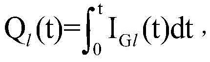
Q为注入的热电子数量,IG为第二电流表的稳定电流示数,t为应力时间。Q is the number of hot electrons injected, IG is the steady current indication of the second ammeter, and t is the stress time.
优选地,所述注入电子数量对所述待测器件特性影响的结果、注入电子能量对所述待测器件特性影响的结果和所述栅极电压对热电子效应的影响的结果,包括:输出特性的相对退化量和转移特性的相对退化量。Preferably, the result of the effect of the quantity of injected electrons on the characteristics of the device under test, the result of the effect of the energy of the injected electrons on the characteristics of the device under test, and the result of the effect of the gate voltage on the thermionic effect include: outputting The relative amount of degradation of the properties and the relative amount of degradation of the transfer properties.
优选的,所述输出特性的相对退化量满足以下公式:Preferably, the relative degradation amount of the output characteristic satisfies the following formula:
所述转移特性的相对退化量满足以下公式:The relative degradation amount of the transfer characteristic satisfies the following formula:
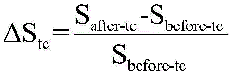
其中,ΔSoutput为所述输出特性的相对退化量,Safter-output为所述第二特性中的所述输出特性,Sbefore-output为所述第一特性中的所述输出特性,ΔStc为所述转移特性的相对退化量,Safter-tc为所述第二特性中的转移特性,Sbefore-tc为所述第一特性中的转移特性。Wherein, ΔS output is the relative degradation amount of the output characteristic, S after-output is the output characteristic in the second characteristic, S before-output is the output characteristic in the first characteristic, ΔS tc is the relative degradation amount of the transfer characteristic, S after-tc is the transfer characteristic in the second characteristic, and S before-tc is the transfer characteristic in the first characteristic.
优选地,该器件在热电子应力实验过程中,源极和漏极接地,整个沟道区可视为0V等势区,而且栅极电压Vg>0,会在整个绝缘层中形成均匀的纵向电场,且方向为从栅极指向沟道。该纵向电场会促进热电子向绝缘层中注入,阻止P型外延层中的空穴向绝缘层注入。因此,热电子应力后,绝缘层的损伤仅由热电子注入引起,与空穴无关。Preferably, during the hot electron stress experiment, the source and drain of the device are grounded, the entire channel region can be regarded as a 0V equipotential region, and the gate voltage Vg>0, which will form a uniform longitudinal direction in the entire insulating layer. Electric field, and the direction is from the gate to the channel. The longitudinal electric field promotes the injection of hot electrons into the insulating layer, and prevents the injection of holes in the P-type epitaxial layer into the insulating layer. Therefore, after hot electron stress, the damage of the insulating layer is only caused by hot electron injection, and has nothing to do with holes.
本发明提供的热电子效应表征方法,注入缓冲层的电子在P+重掺杂区与沟道区之间电场的加速作用下,部分成为热电子。由于源极S、漏极D接地,整个沟道区可视为0V等势区,靠近沟道下方的电场可视为匀强电场,且方向垂直沟道向下,故热电子会均匀地向器件绝缘层注入,有助于深入研究热电子效应。According to the method for characterizing thermionic effect provided by the invention, electrons injected into the buffer layer partially become hot electrons under the acceleration of the electric field between the P+ heavily doped region and the channel region. Since the source S and the drain D are grounded, the entire channel region can be regarded as a 0V equipotential region, and the electric field near the channel can be regarded as a uniform electric field, and the direction is vertical to the channel downward, so the hot electrons will be evenly distributed to the channel. Implantation into device insulating layers, which is helpful for in-depth study of thermionic effects.
实施例三:Embodiment three:
请继续参见图1、图2、图3和图4,并参见图5、图6a-6b和图7a-7b,图8a-8b,图5为本发明提供的一种基于化合物材料MISFET器件的热电子效应表征方法的实现流程图;图6a-6b为本发明提供待测器件输出特性与转移特性的退化量分别随不同热电子注入数量变化的曲线图;图7a-7b为本发明提供待测器件输出特性与转移特性的退化量分别随不同热电子注入能量变化的曲线图;图8a-8b为本发明提供待测器件输出特性与转移特性的退化量分别随不同栅极电压变化的曲线图。本实施例在上述实施例的基础上对该表征方法进行了详细的描述,如图5所示,本发明具体实施步骤如下:Please continue to refer to FIG. 1, FIG. 2, FIG. 3 and FIG. 4, and refer to FIG. 5, FIG. 6a-6b, FIG. 7a-7b, FIG. 8a-8b, FIG. The implementation flow chart of the hot electron effect characterization method; Figures 6a-6b are graphs of the degradation amount of the output characteristics and transfer characteristics of the device under test provided by the present invention with different hot electron injection quantities respectively; Figures 7a-7b are provided by the present invention. Figure 8a-8b is a graph of the degradation of the output characteristics and transfer characteristics of the device under test with different hot electron injection energies respectively; Figures 8a-8b are the curves of the degradation of the output characteristics and transfer characteristics of the device under test with different gate voltages respectively. picture. This embodiment describes the characterization method in detail on the basis of the above-mentioned embodiment. As shown in FIG. 5 , the specific implementation steps of the present invention are as follows:
步骤1,制作测试图形。Step 1, make a test pattern.
选取基于化合物材料MISFET器件,如图2所示,包括:衬底21,P型外延层22、绝缘层23、钝化层24、栅极25、N+掺杂区26、源极27和漏极28;其中,P型外延层22位于衬底21之上,绝缘层23位于P型外延层22之上,钝化层24位于绝缘层23两侧,栅极25位于绝缘层23之上,N+掺杂区26位于P型外延层22内,两个N+掺杂区26对应分布在P型外延层22内,源极27和漏极28穿透钝化层24,且源极27和漏极28分别位于位于N+掺杂区26之上。A MISFET device based on compound materials is selected, as shown in FIG. 2, including:
然后,对MISFET器件的源极27和漏极28两侧的绝缘层23分别进行刻蚀,刻蚀深度与绝缘层23厚度相同,即保留源极27与漏极28之间的P型外延层22,将源极27与漏极28两侧的绝缘层23刻蚀掉,暴露出P型外延层22。接着在源极27和漏极28两侧的P型外延层22表面,由内向外分别制作对称的P+、N+重掺杂区域,并分别在P+、N+重掺杂区域上制作欧姆电极A、B,完成基于MISFET器件的测试结构制备。Then, the insulating
步骤2,进行热电子应力实验。In
选取制作好的器件,即未施加过任何应力的器件,测试应力前器件的第一特性Sbefore。A fabricated device, that is, a device that has not been subjected to any stress, is selected, and the first characteristic S before of the device before stress is tested.
优选的,第一特性包括:输出特性Sbefore-output和转移特性Sbefore-tc。Preferably, the first characteristic includes: an output characteristic S before-output and a transition characteristic S before-tc .
如图3所示,将第一电压源的一端连接电极A,另一端接地;将第二电压源的一端与电极B连接,第二电压源另一端接地;将第三电压源V3的一端与电流表A、栅电极G连接,另一端接地;将源极S和漏极D接地,完成实验电路连接;As shown in Figure 3, one end of the first voltage source is connected to the electrode A, and the other end is grounded; one end of the second voltage source is connected to the electrode B, and the other end of the second voltage source is grounded; one end of the third voltage source V3 is connected to the electrode B. The ammeter A and the gate electrode G are connected, and the other end is grounded; the source S and the drain D are grounded to complete the experimental circuit connection;
优选的,设置第一电压源V1、第二电压源V2、第三电压源V3的电压分别为Va,Vb,Vg,并接通电路进行热电子应力实验,应力持续时间为t秒。Preferably, the voltages of the first voltage source V1, the second voltage source V2, and the third voltage source V3 are set as Va, Vb, and Vg, respectively, and the circuit is turned on to conduct the hot electron stress experiment, and the stress duration is t seconds.
优选的,Vg>0,Vb<Va<0,且Va-Vb>Von,其中,Von为P型外延层与第二N+掺杂区形成pn结的导通电压。Preferably, Vg>0, Vb<Va<0, and Va-Vb>Von, wherein Von is the turn-on voltage for forming a pn junction between the P-type epitaxial layer and the second N+ doped region.
步骤3,测量热电子注入数量对器件的影响。Step 3, measure the effect of the number of hot electron injections on the device.
优选的,如图4所示,当P型外延层内的P/N+结正向导通时,大量电子会从N+区注入P型外延层,故可通过控制P/N+结上所加偏置电压差Va-Vb的大小,来调整热电子注入的数量。同时,将源极S与漏极D悬空,则整个沟道区可视为0V等势区,当P+区施加电压Va-Vb时,会形成自沟道指向P+区的强电场,加速P型外延层中的电子,使之成为高能热电子,故可通过控制V1电压源来控制加速电场的强弱,进而控制热电子注入的能量Preferably, as shown in FIG. 4, when the P/N+ junction in the P-type epitaxial layer is conducting forward, a large number of electrons will be injected into the P-type epitaxial layer from the N+ region, so the bias applied on the P/N+ junction can be controlled by controlling The magnitude of the voltage difference Va-Vb to adjust the amount of hot electron injection. At the same time, if the source S and drain D are suspended, the entire channel region can be regarded as a 0V equipotential region. When the voltage Va-Vb is applied to the P+ region, a strong electric field will be formed from the channel to the P+ region, accelerating the P-type The electrons in the epitaxial layer become high-energy hot electrons, so the strength of the accelerating electric field can be controlled by controlling the V1 voltage source, and then the energy of hot electron injection can be controlled
优选地,由于实验过程中,Vg>0,故栅压形成的电场垂直绝缘层,方向从栅极自上向下指向P型外延层。因此,该电场会阻止P型外延层中的空穴向绝缘层注入,促进P型外延层加速形成的热电子向绝缘层注入,所以栅极电流IG可近似为注入绝缘层的热电子电流。Preferably, since Vg>0 during the experiment, the electric field formed by the gate voltage is perpendicular to the insulating layer, and the direction is from the gate to the P-type epitaxial layer from top to bottom. Therefore, the electric field will prevent the holes in the P-type epitaxial layer from being injected into the insulating layer, and promote the injection of hot electrons formed by the accelerated formation of the P-type epitaxial layer into the insulating layer, so the gate current IG can be approximated as the hot electron current injected into the insulating layer. .
优选的,保持Va值恒定不变,使P型外延层中的加速电场恒定,即保持热电子注入能量不变,通过多次改变(Va-Vb)的差值,来控制热电子的注入数量。其具体操作是:保持Va恒定为-3V,多次改变第二电压源上的电压为Vb(1)=-4V,Vb(2)=-5V,Vb(3)=-6V,则对应P/N+结上的偏压大小为Va-Vb(k),设置Vg=1V,应力持续时间为t秒,重复步骤2,对器件施加应力,分别记录热电子应力前后器件的第一特性Sbefore(k)和第二特性Safter(k),即分别记录应力前后输出特性Sbefore-output(k)和Safter-output(k),以及转移特性Sbefore-tc(k)和Safter-tc(k)。同时,在应力过程中,记录电流表A的稳定示数IGk(t)。Preferably, the value of Va is kept constant, the accelerating electric field in the P-type epitaxial layer is kept constant, that is, the injection energy of hot electrons is kept constant, and the number of hot electrons injected is controlled by changing the difference of (Va-Vb) multiple times. . The specific operation is: keeping Va constant at -3V, changing the voltage on the second voltage source several times to be Vb(1)=-4V, Vb(2)=-5V, Vb(3)=-6V, then the corresponding P The bias voltage on the /N+ junction is Va-Vb(k), set Vg=1V, the stress duration is t seconds,
根据以下公式计算,当热电子应力条件为Va=-3V,Vb(k)分别为-4V,-5V,-6V,Vg=1V时,热电子注入数量的近似值Qk(t):According to the following formula, when the hot electron stress condition is Va=-3V, Vb(k) is -4V, -5V, -6V, Vg=1V, the approximate value of hot electron injection quantity Q k (t):

上式中,t为热电子应力时长,k=1,2,3。In the above formula, t is the hot electron stress duration, k=1, 2, 3.
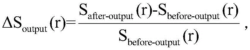
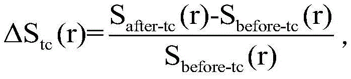
根据应力前后物理参数退化量的定义,可计算出当第二电压源V2上所施加的应力电压为Vb(k)时,待测器件输出特性与转移特性的相对退化量分别为:According to the definition of the degradation amount of physical parameters before and after stress, it can be calculated that when the stress voltage applied to the second voltage source V2 is Vb(k), the relative degradation amounts of the output characteristics and transfer characteristics of the device under test are:
其中,△Soutput(k)指应力电压为Va,Vb(k)时,待测器件在此应力前后输出特性的相对退化量;△Stc(k)指应力电压为Va,Vb(k)时,待测器件在此应力前后转移特性的相对退化量;本实例中k=1,2,3,即给待测器件分别施加了3组不同的电应力。如图6a和图6b所示,本实例通过分析器件在不同应力前后Soutput(k)与△Stc(k)的变化规律,研究热电子注入数量对器件特性的影响。Among them, △S output (k) refers to the relative degradation of the output characteristics of the device under test before and after the stress when the stress voltage is Va, Vb(k); △Stc(k) refers to when the stress voltage is Va, Vb(k) , the relative degradation amount of the transfer characteristic of the device under test before and after the stress; in this example, k=1, 2, 3, that is, three groups of different electrical stresses are applied to the device under test. As shown in Fig. 6a and Fig. 6b, this example studies the influence of the number of hot electron injection on the device characteristics by analyzing the variation law of S output (k) and ΔS tc (k) before and after different stresses.
步骤4、测量热电子注入能量对器件的影响:Step 4. Measure the effect of hot electron injection energy on the device:
保持Va-Vb差值恒定,即保持热电子注入数量不变,通过多次改变Va的值,来调节P型外延层中电子的加速电场,从而控制不同的热电子注入能量。其具体操作是:保持Va(r)-Vb(r)差值恒定为1V,多次改变第一电压源V1上所施加的电压为Va(1)=-3V,Va(2)=-4V,Va(3)=-5V,和第二电压源V2上所施加的电压为Vb(1)=-4V,Vb(2)=-5V,Vb(3)=-6V,设置Vg=1V,应力持续时间为t秒,重复步骤2,对器件施加电应力,分别记录此应力前后器件特性的测试结果Sbefore(r)与Safter(r)。同时,在应力过程中,记录电流表A的稳定示数IGr(t)。Keeping the Va-Vb difference constant, that is, keeping the number of hot electron injections unchanged, and changing the value of Va for many times to adjust the accelerating electric field of electrons in the P-type epitaxial layer, thereby controlling different hot electron injection energies. The specific operation is: keeping the difference between Va(r)-Vb(r) constant at 1V, and changing the voltage applied on the first voltage source V1 to Va(1)=-3V, Va(2)=-4V for many times , Va(3)=-5V, and the voltage applied on the second voltage source V2 is Vb(1)=-4V, Vb(2)=-5V, Vb(3)=-6V, set Vg=1V, The stress duration is t seconds,
根据以下公式计算,当热电子应力条件为Va(r)为-3V,-4V,-5V,相应的Vb(r)分别为-4V,-5V,-6V,且Vg=1V时,热电子注入数量的近似值Qr(t):Calculated according to the following formula, when the hot electron stress condition is that Va(r) is -3V, -4V, -5V, the corresponding Vb(r) is -4V, -5V, -6V, and Vg=1V, the hot electron Approximation of injection quantity Q r (t):

上式中,t为热电子应力时长,r=1,2,3。In the above formula, t is the hot electron stress duration, and r=1, 2, 3.
根据应力前后物理参数退化量的定义,可计算出当第一电压源V1和第二电压源V2上分别施加电压Va(r)与Vb(r)时,待测器件输出特性与转移特性的相对退化量分别为:According to the definition of the degradation of physical parameters before and after stress, when the voltages Va(r) and Vb(r) are respectively applied to the first voltage source V1 and the second voltage source V2, the relative relationship between the output characteristics and the transfer characteristics of the device under test can be calculated. The degradation amounts are:
其中,△Soutput(r)指应力电压为Va(r),Vb(r)时,待测器件在此应力前后输出特性的相对退化量;△Stc(r)指应力电压为Va(r),Vb(r)时,待测器件在此应力前后转移特性参量的相对退化量。本实例中r=1,2,3,即给待测器件分别施加了3组不同的电应力。如图7a和图7b所示,本实例通过分析器件在不同应力前后,△Suotput(r)与△Stc(r)的变化规律,研究热电子注入能量对器件特性的影响。Among them, △S output (r) refers to the relative degradation of the output characteristics of the device under test before and after the stress when the stress voltage is Va(r) and Vb(r); △S tc (r) refers to the stress voltage of Va(r) ), Vb(r), the relative degradation of the transfer characteristic parameters of the device under test before and after the stress. In this example, r=1, 2, and 3, that is, three groups of different electrical stresses are respectively applied to the device under test. As shown in Figure 7a and Figure 7b, this example studies the influence of hot electron injection energy on device characteristics by analyzing the variation law of ΔSuotput (r) and ΔS tc (r) before and after different stresses.
步骤5、测量栅极电压对热电子效应的影响:
保持Va值恒定不变,使P型外延层中的加速电场恒定,即保持热电子注入能量不变。同时保持Va-Vb的差值不变,来控制一定的热电子注入数量,通过多次改变栅压Vg来调控注入绝缘层中热电子的加速电场。其具体操作是:多次改变第三电压源V3上所施加的电压为Vg(1)=1V,Vg(2)=2V,Vg(3)=3V,设置Va=-3V,Vb=-4V,应力持续时间为t秒,重复步骤2,对器件施加电应力,分别记录此应力前后器件特性的测试结果Sbefore(l)与Safter(l)。同时,在应力过程中,记录电流表A的稳定示数IGl(t)。Keeping the value of Va constant, the accelerating electric field in the P-type epitaxial layer is kept constant, that is, the injection energy of hot electrons is kept constant. At the same time, the difference between Va-Vb is kept unchanged to control a certain number of hot electrons injected, and the accelerating electric field of hot electrons injected into the insulating layer is regulated by changing the gate voltage Vg multiple times. The specific operation is: changing the voltage applied on the third voltage source V3 to Vg(1)=1V, Vg(2)=2V, Vg(3)=3V many times, setting Va=-3V, Vb=-4V , the stress duration is t seconds,
根据以下公式计算,当热电子应力条件为Va=-3V,Vb=-4V,Vg(l)分别为1V,2V,3V时,热电子注入数量的近似值Ql(t):Calculated according to the following formula, when the hot electron stress conditions are Va=-3V, Vb=-4V, and Vg(l) are 1V, 2V, 3V, respectively, the approximate value of hot electron injection quantity Q l (t):
上式中,t为热电子应力时长,l=1,2,3。In the above formula, t is the hot electron stress duration, and l=1, 2, 3.
根据应力前后物理参数退化量的定义,可计算出当第三电压源V3上分别施加电压Vg(l)时,待测器件输出特性与转移特性的相对退化量分别为:According to the definition of the degradation amount of physical parameters before and after stress, when the voltage Vg(l) is applied to the third voltage source V3 respectively, the relative degradation amounts of the output characteristics and transfer characteristics of the device under test can be calculated as:


其中,ΔSoutput(l)指栅极电压为Vg(l)时,待测器件在此应力前后输出特性的相对退化量;ΔStc(l)指栅极电压为Vg(l)时,待测器件在此应力前后转移特性参量的相对退化量。本实例中l=1,2,3,即给待测器件分别施加了3组不同的栅极电压应力。如图8a和图8b所示,本实例通过分析器件在不同应力前后,ΔSoutput(l)与ΔStc(l)的变化规律,研究栅极电压对器件热电子效应的影响。Among them, ΔS output (l) refers to the relative degradation of the output characteristics of the device under test before and after the stress when the gate voltage is Vg(l); The relative amount of degradation in the transfer characteristic parameters of the device before and after this stress. In this example, l=1, 2, and 3, that is, three groups of different gate voltage stresses are applied to the device under test. As shown in Figure 8a and Figure 8b, this example studies the influence of gate voltage on the hot electron effect of the device by analyzing the variation law of ΔS output (l) and ΔS tc (l) before and after different stresses.
优选地,本发明所涉及的被测器件为化合物材料MISFET器件,该化合物半导体材料包括但不限于砷化镓(GaAs)、氮化镓(GaN)、氧化镓(GaO)、磷化铟(InP)和碳化硅(SiC)等,本实例的被测器件为GaN基MISFET器件。Preferably, the device under test involved in the present invention is a compound material MISFET device, and the compound semiconductor material includes but is not limited to gallium arsenide (GaAs), gallium nitride (GaN), gallium oxide (GaO), indium phosphide (InP) ) and silicon carbide (SiC), etc., the device under test in this example is a GaN-based MISFET device.
本实施例提供了一种热电子注入数量与能量可控技术的化合物材料MISFET器件的表征方法,通过调整电压Va和Vb来控制绝缘层中热电子的注入数量,并通过调整电压Va来控制绝缘层中热电子的注入能量,解决了器件热电子注入数量和注入能量的不可控,以及非均匀注入绝缘层等问题,有助于对化合物材料MISFET器件中的热电子效应进行深入分析。This embodiment provides a method for characterizing a compound material MISFET device with controllable thermionic injection quantity and energy. The injection quantity of hot electrons in the insulating layer is controlled by adjusting the voltages Va and Vb, and the insulation is controlled by adjusting the voltage Va. The injection energy of hot electrons in the layer solves the problems of uncontrollable hot electron injection quantity and injection energy, as well as non-uniform injection into the insulating layer, which is helpful for in-depth analysis of the hot electron effect in compound material MISFET devices.
以上内容是结合具体的优选实施方式对本发明所作的进一步详细说明,不能认定本发明的具体实施只局限于这些说明。对于本发明所属技术领域的普通技术人员来说,在不脱离本发明构思的前提下,还可以做出若干简单推演或替换,都应当视为属于本发明的保护范围。The above content is a further detailed description of the present invention in combination with specific preferred embodiments, and it cannot be considered that the specific implementation of the present invention is limited to these descriptions. For those of ordinary skill in the technical field of the present invention, without departing from the concept of the present invention, some simple deductions or substitutions can be made, which should be regarded as belonging to the protection scope of the present invention.
Claims (10)


Priority Applications (1)
| Application Number | Priority Date | Filing Date | Title |
|---|---|---|---|
| CN201910173484.2A CN111668190B (en) | 2019-03-07 | 2019-03-07 | Hot electron effect characterization method based on compound material MISFET device |
Applications Claiming Priority (1)
| Application Number | Priority Date | Filing Date | Title |
|---|---|---|---|
| CN201910173484.2A CN111668190B (en) | 2019-03-07 | 2019-03-07 | Hot electron effect characterization method based on compound material MISFET device |
Publications (2)
| Publication Number | Publication Date |
|---|---|
| CN111668190A CN111668190A (en) | 2020-09-15 |
| CN111668190B true CN111668190B (en) | 2021-11-19 |
Family
ID=72382161
Family Applications (1)
| Application Number | Title | Priority Date | Filing Date |
|---|---|---|---|
| CN201910173484.2A Active CN111668190B (en) | 2019-03-07 | 2019-03-07 | Hot electron effect characterization method based on compound material MISFET device |
Country Status (1)
| Country | Link |
|---|---|
| CN (1) | CN111668190B (en) |
Citations (5)
| Publication number | Priority date | Publication date | Assignee | Title |
|---|---|---|---|---|
| US4382229A (en) * | 1980-11-28 | 1983-05-03 | International Business Machines Corporation | Channel hot electron monitor |
| US5533197A (en) * | 1994-10-21 | 1996-07-02 | International Business Machines Corporation | Method to assess electromigration and hot electron reliability for microprocessors |
| TW201027535A (en) * | 2009-01-13 | 2010-07-16 | Winbond Electronics Corp | Method for determining native threshold voltage of nonvolatile memory |
| CN103869230A (en) * | 2014-01-20 | 2014-06-18 | 南京大学 | Method for representing local distribution of interface state and oxide layer trap in small-sized CMOS device |
| CN106356313A (en) * | 2016-11-04 | 2017-01-25 | 东南大学 | Test method for lateral insulated gate bipolar transistor interface state and five-port device |
Family Cites Families (1)
| Publication number | Priority date | Publication date | Assignee | Title |
|---|---|---|---|---|
| JP3667676B2 (en) * | 2001-10-11 | 2005-07-06 | 株式会社東芝 | Semiconductor device, semiconductor device manufacturing method, and electrical characteristics evaluation system for semiconductor device |
-
2019
- 2019-03-07 CN CN201910173484.2A patent/CN111668190B/en active Active
Patent Citations (5)
| Publication number | Priority date | Publication date | Assignee | Title |
|---|---|---|---|---|
| US4382229A (en) * | 1980-11-28 | 1983-05-03 | International Business Machines Corporation | Channel hot electron monitor |
| US5533197A (en) * | 1994-10-21 | 1996-07-02 | International Business Machines Corporation | Method to assess electromigration and hot electron reliability for microprocessors |
| TW201027535A (en) * | 2009-01-13 | 2010-07-16 | Winbond Electronics Corp | Method for determining native threshold voltage of nonvolatile memory |
| CN103869230A (en) * | 2014-01-20 | 2014-06-18 | 南京大学 | Method for representing local distribution of interface state and oxide layer trap in small-sized CMOS device |
| CN106356313A (en) * | 2016-11-04 | 2017-01-25 | 东南大学 | Test method for lateral insulated gate bipolar transistor interface state and five-port device |
Non-Patent Citations (1)
| Title |
|---|
| GaAsPHEMT器件的退化特性及可靠性表征方法;刘红侠;《半导体学报》;20040108;第25卷(第1期);77-80页 * |
Also Published As
| Publication number | Publication date |
|---|---|
| CN111668190A (en) | 2020-09-15 |
Similar Documents
| Publication | Publication Date | Title |
|---|---|---|
| Zagni et al. | “Hole Redistribution” Model Explaining the Thermally Activated R ON Stress/Recovery Transients in Carbon-Doped AlGaN/GaN Power MIS-HEMTs | |
| US12112945B2 (en) | Semiconductor wafer, electronic device, method of performing inspection on semiconductor wafer, and method of manufacturing electronic device | |
| Chandrasekar et al. | Buffer-induced current collapse in GaN HEMTs on highly resistive Si substrates | |
| Modolo et al. | Cumulative hot-electron trapping in GaN-based power HEMTs observed by an ultrafast (10 V/Ns) on-wafer methodology | |
| Yu et al. | Dynamic characterizations of AlGaN/GaN HEMTs with field plates using a double-gate structure | |
| Barbato et al. | Fast System to measure the dynamic on‐resistance of on‐wafer 600 V normally off GaN HEMTs in hard‐switching application conditions | |
| Butej et al. | Method to distinguish between buffer and surface trapping in stressed normally-ON GaN GITs using the gate-voltage dependence of recovery time constants | |
| Zagni et al. | Mechanisms underlying the bidirectional V T shift after negative-bias temperature Instability stress in carbon-Doped fully recessed AlGaN/GaN MIS-HEMTs | |
| Hua et al. | Hole-Induced Degradation in ${E} $-Mode GaN MIS-FETs: Impact of Substrate Terminations | |
| Zhu et al. | Characterization and analysis on performance and avalanche reliability of SiC MOSFETs with varied JFET region width | |
| CN111668190B (en) | Hot electron effect characterization method based on compound material MISFET device | |
| Shi et al. | The chip-level and package-level degradation of cascode GaN device under repetitive power cycling stress | |
| CN111668189B (en) | Thermal electron effect test structure of MIS-HEMT device and characterization method thereof | |
| CN111668127B (en) | Hot electron effect test structure based on HEMT device and characterization method thereof | |
| Zhang et al. | Study on the Dynamic R on Degradation in GaN-based Power HEMT | |
| Feng et al. | Dynamic performance analysis of p-GaN HEMTs with floating substrates by substrate capacitance coupling model | |
| CN111668126B (en) | Test structure and characterization method of hot hole effect in a compound MISFET device | |
| CN107078153A (en) | The field-effect transistor and its manufacture method of mixing drain contact with optimization | |
| CN117928769B (en) | A method for determining channel carrier temperature of gallium nitride device | |
| CN102565660A (en) | An ultra-high-speed Id-Vg test method applied to MOSFETs devices | |
| Rrustemi et al. | Reliable method for low field temperature dependent mobility extraction at Al 2 O 3/GaN interface | |
| Mao et al. | Trapping and gate leakage currents effects in large signal modeling of microwave GaN HEMTs | |
| Kim et al. | Analysis on effect of hot-carrier-induced degradation of NPT-IGBT | |
| Franchi et al. | 1200 V SiC MOSFETs with Stable VTH under High Temperature Gate Bias Stress | |
| Suzuki et al. | Unique short-circuit failure mechanisms in 1.2-kV SiC planar MOSFETs |
Legal Events
| Date | Code | Title | Description |
|---|---|---|---|
| PB01 | Publication | ||
| PB01 | Publication | ||
| SE01 | Entry into force of request for substantive examination | ||
| SE01 | Entry into force of request for substantive examination | ||
| GR01 | Patent grant | ||
| GR01 | Patent grant |