CN111180454B - 3D memory device and method of manufacturing the same - Google Patents
3D memory device and method of manufacturing the same Download PDFInfo
- Publication number
- CN111180454B CN111180454B CN202010001944.6A CN202010001944A CN111180454B CN 111180454 B CN111180454 B CN 111180454B CN 202010001944 A CN202010001944 A CN 202010001944A CN 111180454 B CN111180454 B CN 111180454B
- Authority
- CN
- China
- Prior art keywords
- layer
- forming
- filling layer
- stacked
- dummy channel
- Prior art date
- Legal status (The legal status is an assumption and is not a legal conclusion. Google has not performed a legal analysis and makes no representation as to the accuracy of the status listed.)
- Active
Links
Images


Classifications
-
- H—ELECTRICITY
- H10—SEMICONDUCTOR DEVICES; ELECTRIC SOLID-STATE DEVICES NOT OTHERWISE PROVIDED FOR
- H10B—ELECTRONIC MEMORY DEVICES
- H10B41/00—Electrically erasable-and-programmable ROM [EEPROM] devices comprising floating gates
- H10B41/30—Electrically erasable-and-programmable ROM [EEPROM] devices comprising floating gates characterised by the memory core region
- H10B41/35—Electrically erasable-and-programmable ROM [EEPROM] devices comprising floating gates characterised by the memory core region with a cell select transistor, e.g. NAND
-
- H—ELECTRICITY
- H10—SEMICONDUCTOR DEVICES; ELECTRIC SOLID-STATE DEVICES NOT OTHERWISE PROVIDED FOR
- H10B—ELECTRONIC MEMORY DEVICES
- H10B41/00—Electrically erasable-and-programmable ROM [EEPROM] devices comprising floating gates
- H10B41/20—Electrically erasable-and-programmable ROM [EEPROM] devices comprising floating gates characterised by three-dimensional arrangements, e.g. with cells on different height levels
- H10B41/23—Electrically erasable-and-programmable ROM [EEPROM] devices comprising floating gates characterised by three-dimensional arrangements, e.g. with cells on different height levels with source and drain on different levels, e.g. with sloping channels
- H10B41/27—Electrically erasable-and-programmable ROM [EEPROM] devices comprising floating gates characterised by three-dimensional arrangements, e.g. with cells on different height levels with source and drain on different levels, e.g. with sloping channels the channels comprising vertical portions, e.g. U-shaped channels
-
- H—ELECTRICITY
- H10—SEMICONDUCTOR DEVICES; ELECTRIC SOLID-STATE DEVICES NOT OTHERWISE PROVIDED FOR
- H10B—ELECTRONIC MEMORY DEVICES
- H10B41/00—Electrically erasable-and-programmable ROM [EEPROM] devices comprising floating gates
- H10B41/40—Electrically erasable-and-programmable ROM [EEPROM] devices comprising floating gates characterised by the peripheral circuit region
- H10B41/41—Electrically erasable-and-programmable ROM [EEPROM] devices comprising floating gates characterised by the peripheral circuit region of a memory region comprising a cell select transistor, e.g. NAND
-
- H—ELECTRICITY
- H10—SEMICONDUCTOR DEVICES; ELECTRIC SOLID-STATE DEVICES NOT OTHERWISE PROVIDED FOR
- H10B—ELECTRONIC MEMORY DEVICES
- H10B41/00—Electrically erasable-and-programmable ROM [EEPROM] devices comprising floating gates
- H10B41/40—Electrically erasable-and-programmable ROM [EEPROM] devices comprising floating gates characterised by the peripheral circuit region
- H10B41/42—Simultaneous manufacture of periphery and memory cells
-
- H—ELECTRICITY
- H10—SEMICONDUCTOR DEVICES; ELECTRIC SOLID-STATE DEVICES NOT OTHERWISE PROVIDED FOR
- H10B—ELECTRONIC MEMORY DEVICES
- H10B43/00—EEPROM devices comprising charge-trapping gate insulators
- H10B43/20—EEPROM devices comprising charge-trapping gate insulators characterised by three-dimensional arrangements, e.g. with cells on different height levels
- H10B43/23—EEPROM devices comprising charge-trapping gate insulators characterised by three-dimensional arrangements, e.g. with cells on different height levels with source and drain on different levels, e.g. with sloping channels
- H10B43/27—EEPROM devices comprising charge-trapping gate insulators characterised by three-dimensional arrangements, e.g. with cells on different height levels with source and drain on different levels, e.g. with sloping channels the channels comprising vertical portions, e.g. U-shaped channels
-
- H—ELECTRICITY
- H10—SEMICONDUCTOR DEVICES; ELECTRIC SOLID-STATE DEVICES NOT OTHERWISE PROVIDED FOR
- H10B—ELECTRONIC MEMORY DEVICES
- H10B43/00—EEPROM devices comprising charge-trapping gate insulators
- H10B43/30—EEPROM devices comprising charge-trapping gate insulators characterised by the memory core region
- H10B43/35—EEPROM devices comprising charge-trapping gate insulators characterised by the memory core region with cell select transistors, e.g. NAND
-
- H—ELECTRICITY
- H10—SEMICONDUCTOR DEVICES; ELECTRIC SOLID-STATE DEVICES NOT OTHERWISE PROVIDED FOR
- H10B—ELECTRONIC MEMORY DEVICES
- H10B43/00—EEPROM devices comprising charge-trapping gate insulators
- H10B43/40—EEPROM devices comprising charge-trapping gate insulators characterised by the peripheral circuit region
Landscapes
- Engineering & Computer Science (AREA)
- Manufacturing & Machinery (AREA)
- Semiconductor Memories (AREA)
- Non-Volatile Memory (AREA)
Abstract
本申请公开了一种3D存储器件及其制造方法。该制造方法包括:在衬底上形成第一叠层结构,包括交替堆叠的多个层间绝缘层与栅极导体层,第一叠层结构具有第一台阶结构;形成覆盖第一台阶结构与衬底的第一填充层;形成覆盖第一叠层结构的第二叠层结构,包括交替堆叠的多个层间绝缘层与栅极导体层,第二叠层结构具有第二台阶结构;形成多个第一虚拟沟道柱,第一虚拟沟道柱的至少部分位于第二台阶结构中,至少一个第一虚拟沟道柱的顶面为第二台阶结构的台阶面。该制造方法通过将虚拟沟道柱的顶面与台阶结构的台阶面共面,解决了器件平整度差的问题。
The application discloses a 3D storage device and a manufacturing method thereof. The manufacturing method includes: forming a first stacked structure on a substrate, including a plurality of interlayer insulating layers and gate conductor layers stacked alternately, the first stacked structure has a first stepped structure; forming a layer covering the first stepped structure and The first filling layer of the substrate; forming a second stacked structure covering the first stacked structure, including a plurality of interlayer insulating layers and gate conductor layers stacked alternately, the second stacked structure has a second stepped structure; forming A plurality of first dummy channel pillars, at least part of the first dummy channel pillars are located in the second stepped structure, and the top surface of at least one first dummy channel pillar is the stepped surface of the second stepped structure. The manufacturing method solves the problem of poor flatness of the device by making the top surface of the dummy channel column coplanar with the step surface of the step structure.
Description
技术领域technical field
本发明涉及存储器技术,更具体地,涉及3D存储器件及其制造方法。The present invention relates to memory technology, and more particularly, to 3D memory devices and manufacturing methods thereof.
背景技术Background technique
半导体技术的发展方向是特征尺寸的减小和集成度的提高。对于存储器件而言,存储器件的存储密度的提高与半导体制造工艺的进步密切相关。随着半导体制造工艺的特征尺寸越来越小,存储器件的存储密度越来越高。The development direction of semiconductor technology is the reduction of feature size and the improvement of integration. For storage devices, the improvement of the storage density of the storage device is closely related to the progress of the semiconductor manufacturing process. As the feature size of the semiconductor manufacturing process becomes smaller and smaller, the storage density of the memory device becomes higher and higher.
为了进一步提高存储密度,已经开发出三维结构的存储器件(即,3D存储器件)。该3D存储器件包括沿着垂直方向堆叠的多个存储单元,在单位面积的晶片上可以成倍地提高集成度,并且可以降低成本。In order to further increase storage density, memory devices with a three-dimensional structure (ie, 3D memory devices) have been developed. The 3D storage device includes a plurality of storage units stacked along the vertical direction, the integration degree can be doubled on a unit area wafer, and the cost can be reduced.
在3D存储器件中,一般采用栅叠层结构以及沟道柱提供选择晶体管和存储晶体管,采用导电通道形成外围电路与存储单元的互联,随着栅叠层结构堆叠的层数不断增加,需要分别形成两个堆叠的栅叠层结构,并分别形成上下沟道孔,存在沟道孔对准效果不好以及器件的平整度差的问题。因此,希望进一步改进3D存储器件的制造工艺,从而提高3D存储器件的良率。In 3D memory devices, gate stack structures and channel pillars are generally used to provide selection transistors and storage transistors, and conductive channels are used to form the interconnection between peripheral circuits and memory cells. As the number of stacked layers in gate stack structures continues to increase, separate Two stacked gate stack structures are formed, and the upper and lower channel holes are formed respectively, which has the problems of poor alignment of the channel holes and poor flatness of the device. Therefore, it is desired to further improve the manufacturing process of the 3D memory device, so as to increase the yield of the 3D memory device.
发明内容Contents of the invention
本发明的目的是提供一种改进的3D存储器件及其制造方法,通过将虚拟沟道柱的顶面与台阶结构的台阶面共面,解决了器件平整度差的问题。The object of the present invention is to provide an improved 3D memory device and its manufacturing method, which solves the problem of poor flatness of the device by making the top surface of the dummy channel column coplanar with the step surface of the step structure.
根据本发明的一方面,提供了一种3D存储器件的制造方法,包括:在衬底上形成第一叠层结构,包括交替堆叠的多个层间绝缘层与栅极导体层,所述第一叠层结构具有第一台阶结构;形成覆盖所述第一台阶结构与所述衬底的第一填充层;形成覆盖所述第一叠层结构的第二叠层结构,包括交替堆叠的多个层间绝缘层与栅极导体层,所述第二叠层结构具有第二台阶结构;形成多个第一虚拟沟道柱,所述第一虚拟沟道柱的至少部分位于所述第二台阶结构中,至少一个所述第一虚拟沟道柱的顶面为所述第二台阶结构的台阶面。According to one aspect of the present invention, a method for manufacturing a 3D memory device is provided, including: forming a first stacked structure on a substrate, including a plurality of interlayer insulating layers and gate conductor layers stacked alternately, the first A laminated structure has a first stepped structure; forming a first filling layer covering the first stepped structure and the substrate; forming a second laminated structure covering the first laminated structure, including alternately stacked multiple an interlayer insulating layer and a gate conductor layer, the second stacked structure has a second stepped structure; a plurality of first dummy channel columns are formed, at least part of the first dummy channel columns are located in the second In the stepped structure, the top surface of at least one of the first dummy channel pillars is the stepped surface of the second stepped structure.
可选地,在形成所述第二台阶结构之前,形成所述第一虚拟沟道柱的方法包括:形成多个第一牺牲结构,所述多个第一牺牲结构自所述第一叠层结构表面向所述衬底方向延伸并穿过所述第一叠层结构,所述第二叠层结构覆盖所述多个第一牺牲结构;形成穿过所述第二叠层结构的多个第一虚拟沟道孔,以暴露对应的所述第一牺牲结构;经所述第一虚拟沟道孔去除所述第一牺牲结构以延伸所述第一虚拟沟道孔,使所述第一虚拟沟道孔依次穿过所述第二叠层结构与所述第一叠层结构;以及在所述第一虚拟沟道孔中形成第一虚拟沟道柱。Optionally, before forming the second stepped structure, the method for forming the first dummy channel pillar includes: forming a plurality of first sacrificial structures, the plurality of first sacrificial structures formed from the first stack The surface of the structure extends toward the substrate and passes through the first stacked structure, and the second stacked structure covers the plurality of first sacrificial structures; forming a plurality of sacrificial structures passing through the second stacked structure a first dummy channel hole to expose the corresponding first sacrificial structure; removing the first sacrificial structure through the first dummy channel hole to extend the first dummy channel hole so that the first A dummy channel hole passes through the second stacked structure and the first stacked structure in sequence; and a first dummy channel column is formed in the first dummy channel hole.
可选地,形成所述第二台阶结构的方法包括:在形成所述第一虚拟沟道柱之后,同时刻蚀所述第一虚拟沟道柱与所述第二叠层结构形成所述第二台阶结构。Optionally, the method for forming the second stepped structure includes: after forming the first dummy channel pillar, simultaneously etching the first dummy channel pillar and the second stacked structure to form the first dummy channel pillar. Two-step structure.
可选地,还包括形成多个第二虚拟沟道柱,至少一个所述第二虚拟沟道柱自所述第一填充层向所述衬底方向延伸,所述第二虚拟沟道柱的至少部分位于所述第一台阶结构中。Optionally, further comprising forming a plurality of second dummy channel pillars, at least one of the second dummy channel pillars extends from the first filling layer toward the substrate, and the second dummy channel pillars at least partly located in the first stepped structure.
可选地,在形成所述第二台阶结构之前,所述第二叠层结构还覆盖所述第一填充层,形成所述第二虚拟沟道柱的方法包括:形成多个第二牺牲结构,所述多个第二牺牲结构自第一填充层表面向所述衬底方向延伸并穿过所述第一填充层与所述第一台阶结构,所述第二叠层结构覆盖所述多个第二牺牲结构;形成穿过所述第二叠层结构的多个第二虚拟沟道孔,以暴露对应的所述第二牺牲结构;经所述第二虚拟沟道孔去除所述第二牺牲结构以延伸所述第二虚拟沟道孔,使所述第二虚拟沟道孔依次穿过所述第二叠层结构、所述第一填充层以及所述第一台阶结构;以及在所述第二虚拟沟道孔中形成第二虚拟沟道柱,其中,在形成所述第二台阶结构时,所述第一填充层上方的所述第二叠层结构与所述第二虚拟沟道柱被去除。Optionally, before forming the second stepped structure, the second stacked structure also covers the first filling layer, and the method for forming the second dummy channel pillar includes: forming a plurality of second sacrificial structures , the plurality of second sacrificial structures extend from the surface of the first filling layer toward the substrate and pass through the first filling layer and the first step structure, and the second stacked structure covers the multiple a second sacrificial structure; forming a plurality of second dummy channel holes through the second stacked structure to expose the corresponding second sacrificial structure; removing the first dummy channel holes through the second dummy channel holes two sacrificial structures to extend the second dummy channel hole so that the second dummy channel hole passes through the second stacked structure, the first filling layer and the first stepped structure in sequence; and A second dummy channel column is formed in the second dummy channel hole, wherein when the second stepped structure is formed, the second stacked structure above the first filling layer and the second dummy The channel posts are removed.
可选地,在形成所述第二台阶结构之前,所述制造方法还包括:在核心区形成多个存储沟道柱,穿过所述二叠层结构与所述第一叠层结构,所述核心区与所述第二台阶结构相邻;对所述存储沟道柱进行回刻蚀以形成多个接触孔;以及形成覆盖所述第二叠层结构的停止层,部分所述停止层填充在所述接触孔中作为插塞结构;以及去除部分停止层,并保留位于核心区的停止层,在形成所述第二填充层之后,所述制造方法还包括:研磨所述第二填充层以对所述第二填充层进行初次平坦化处理,其中,研磨在到达所述停止层时停止。Optionally, before forming the second stepped structure, the manufacturing method further includes: forming a plurality of storage channel pillars in the core region, passing through the second stacked structure and the first stacked structure, so The core region is adjacent to the second stepped structure; etching back the storage channel column to form a plurality of contact holes; and forming a stop layer covering the second stacked structure, part of the stop layer filling in the contact hole as a plug structure; and removing part of the stop layer, and retaining the stop layer located in the core area, after forming the second filling layer, the manufacturing method further includes: grinding the second filling layer layer to perform an initial planarization process on the second fill layer, wherein grinding is stopped upon reaching the stop layer.
可选地,在对所述第二填充层进行初步平坦化处理之后,所述制造方法还包括:去除所述停止层的一部分,并保留所述插塞结构;以及研磨所述第二填充层以对所述第二填充层进行二次平坦化处理,其中,研磨在到达所述插塞结构时停止。Optionally, after performing a preliminary planarization process on the second filling layer, the manufacturing method further includes: removing a part of the stop layer, and retaining the plug structure; and grinding the second filling layer A secondary planarization process is performed on the second filling layer, wherein grinding stops when reaching the plug structure.
可选地,所述去除部分停止层的步骤包括:在所述停止层上形成光刻掩模;以及采用刻蚀工艺将所述光刻掩模的图案转移至所述停止层上,其中,形成第二台阶结构的步骤包括:采用刻蚀工艺将所述光刻掩模的图案转移至靠近所述停止层的所述层间绝缘层与所述牺牲层上以形成所述第二台阶结构的顶部台阶。Optionally, the step of removing part of the stop layer includes: forming a photolithography mask on the stop layer; and transferring the pattern of the photolithography mask to the stop layer by an etching process, wherein, The step of forming the second stepped structure includes: using an etching process to transfer the pattern of the photolithography mask to the interlayer insulating layer and the sacrificial layer close to the stop layer to form the second stepped structure top steps.
可选地,所述停止层的材料包括多晶硅。Optionally, the material of the stop layer includes polysilicon.
可选地,所述第一台阶结构在平行于所述衬底的方向上突出于所述第二台阶结构。Optionally, the first stepped structure protrudes from the second stepped structure in a direction parallel to the substrate.
可选地,所述第一填充层与所述第二填充层的材料包括正硅酸乙酯。Optionally, materials of the first filling layer and the second filling layer include tetraethyl orthosilicate.
根据本发明的另一方面,提供了一种3D存储器件,包括:衬底;第一叠层结构,位于所述衬底上,包括交替堆叠的多个层间绝缘层与栅极导体层,所述第一叠层结构具有第一台阶结构;第一填充层,覆盖所述第一台阶结构及所述衬底;第二叠层结构,覆盖所述第一叠层结构,包括交替堆叠的多个层间绝缘层与栅极导体层,所述第二叠层结构具有第二台阶结构;第二填充层,覆盖所述第二台阶结构与所述第一填充层;以及若干第一虚拟沟道柱,所述第一虚拟沟道柱的至少部分位于所述第二台阶结构中,至少一个所述第一虚拟沟道柱的顶面为所述第二台阶结构的台阶面。According to another aspect of the present invention, a 3D memory device is provided, including: a substrate; a first stacked structure located on the substrate, including a plurality of interlayer insulating layers and gate conductor layers stacked alternately, The first stacked structure has a first stepped structure; the first filling layer covers the first stepped structure and the substrate; the second stacked structure covers the first stacked structure, including alternately stacked A plurality of interlayer insulating layers and gate conductor layers, the second stacked structure has a second stepped structure; a second filling layer covering the second stepped structure and the first filling layer; and several first dummy layers Channel pillars, at least part of the first dummy channel pillars are located in the second stepped structure, and the top surface of at least one of the first dummy channel pillars is a stepped surface of the second stepped structure.
可选地,还包括若干第二虚拟沟道柱,至少一个所述第二虚拟沟道柱自所述第一填充层向所述衬底方向延伸,所述第二虚拟沟道柱的至少部分位于所述第一台阶结构中。Optionally, it also includes several second dummy channel pillars, at least one of the second dummy channel pillars extends from the first filling layer toward the substrate, at least part of the second dummy channel pillars located in the first stepped structure.
可选地,所述第一台阶结构在平行于所述衬底的方向上突出于所述第二台阶结构。Optionally, the first stepped structure protrudes from the second stepped structure in a direction parallel to the substrate.
可选地,还包括:多个存储沟道柱,在核心区穿过所述第二叠层结构与所述第一叠层结构,所述核心区与所述第二台阶结构所在区域相邻;插塞结构,位于所述存储沟道柱上,其中,所述第二填充层的表面与所述插塞结构的表面平齐。Optionally, it further includes: a plurality of storage channel columns passing through the second stacked structure and the first stacked structure in the core area, and the core area is adjacent to the area where the second stepped structure is located a plug structure located on the storage channel pillar, wherein the surface of the second filling layer is flush with the surface of the plug structure.
可选地,所述插塞结构的材料包括多晶硅。Optionally, the material of the plug structure includes polysilicon.
可选地,所述第一填充层与所述第二填充层的材料包括正硅酸乙酯。Optionally, materials of the first filling layer and the second filling layer include tetraethyl orthosilicate.
根据本发明实施例提供的3D存储器件及其制造方法,通过将至少部分的第一虚拟沟道柱顶面作为第二台阶结构的台阶面,在覆盖第二台阶结构与第一填充结构形成第二填充层时,不会受到第一虚拟沟道柱的影响,使得第二填充层的结构完整,材料、应力分布均匀,从而提高了器件的平整度。According to the 3D memory device and its manufacturing method provided by the embodiments of the present invention, by using at least part of the top surface of the first dummy channel column as the step surface of the second step structure, the second step structure is formed covering the second step structure and the first filling structure. When the second filling layer is used, it will not be affected by the first virtual channel column, so that the structure of the second filling layer is complete, and the distribution of material and stress is uniform, thereby improving the flatness of the device.
进一步的,由于第二填充层的结构完整,材料、应力分布均匀,在后续研磨过程中,在台阶位置处仅需要对第二填充层进行研磨,更容易对研磨的相关工艺参数进行控制。Further, since the structure of the second filling layer is complete and the material and stress distribution are uniform, only the second filling layer needs to be ground at the step position during the subsequent grinding process, and it is easier to control the relevant process parameters of grinding.
进一步的,由于第二填充层在形成第二台阶结构之后形成,而第一虚拟沟道孔与第二虚拟沟道孔在形成第二台阶结构之前形成,因此在形成第一虚拟沟道孔与第二虚拟沟道孔时,仅需要贯穿第二叠层结构,并不会涉及第二填充层的刻蚀,由于第二叠层结构应力均匀,不需要在形成沟道孔之前进行退火,防止了由于退火造成第一叠层结构与第一填充层的形变问题,从而使得沟道孔与牺牲结构可以容易地对准。与此同时,由于不需要刻蚀除第二叠层结构以外的材料(例如常规工艺中台阶区的填充层),降低了刻蚀难度,节省了刻蚀成本。Further, since the second filling layer is formed after forming the second stepped structure, and the first dummy channel hole and the second dummy channel hole are formed before forming the second stepped structure, therefore, after forming the first dummy channel hole and the second dummy channel hole, For the second dummy channel hole, it only needs to penetrate the second stacked structure, and does not involve the etching of the second filling layer. Since the second stacked structure has uniform stress, it is not necessary to perform annealing before forming the channel hole, preventing The problem of deformation of the first stacked structure and the first filling layer due to annealing is solved, so that the channel hole and the sacrificial structure can be easily aligned. At the same time, since there is no need to etch materials other than the second stacked structure (for example, the filling layer of the step region in the conventional process), the etching difficulty is reduced and the etching cost is saved.
进一步的,通过覆盖第二叠层结构形成停止层,并将位于接触孔中的停止层复用作为每个沟道柱的插塞结构,在对第二填充层进行初步平坦化处理时,停止层的表面可以作为研磨的停止标记,在对第二填充层进行二次平坦化处理时,插塞结构的表面可以作为研磨的停止标记,由于在本实施中,已经通过同一停止层形成了两次研磨的停止标记,不再需要常规研磨工艺中的位于第二填充层表面的氮化硅停止层作为停止标记,节省了形成氮化硅停止层的工艺步骤,也避免了在常规工艺中光刻胶在氮化硅停止层上残留的问题。Further, the stop layer is formed by covering the second stacked structure, and the stop layer located in the contact hole is reused as the plug structure of each channel column. When the second filling layer is initially planarized, the stop layer The surface of the plug structure can be used as a stop mark for grinding. When the second filling layer is planarized, the surface of the plug structure can be used as a stop mark for grinding. The stop mark of the secondary grinding does not need the silicon nitride stop layer on the surface of the second filling layer in the conventional grinding process as the stop mark, which saves the process steps of forming the silicon nitride stop layer and avoids the need for light in the conventional process. The problem of resist residue on the silicon nitride stop layer.
进一步的,在去除位于台阶区的停止层时,通过将同一个光刻掩模的图案分别转移到停止层和靠近停止层的层间绝缘层与牺牲层上,不仅利用保留的停止层作为在对第二填充层进行初次平坦化处理时的研磨停止标记,同时通过刻蚀靠近停止层的层间绝缘层与牺牲层形成了顶部的第二台阶结构,从而省去了用于顶部的第二台阶结构的光刻修饰(trim)步骤。Further, when removing the stop layer located in the step region, by transferring the pattern of the same photolithography mask to the stop layer and the interlayer insulating layer and the sacrificial layer close to the stop layer, not only the remaining stop layer is used as the The grinding stop mark when the first planarization process is performed on the second filling layer, and at the same time, the second step structure at the top is formed by etching the interlayer insulating layer and the sacrificial layer close to the stop layer, thereby eliminating the need for the second step structure for the top. Photolithographic trimming (trim) step of the stepped structure.
因此,根据本发明实施例的半导体器件及其制造方法提高了产品良率和可靠性。Therefore, the semiconductor device and the manufacturing method thereof according to the embodiments of the present invention improve product yield and reliability.
附图说明Description of drawings
通过以下参照附图对本发明实施例的描述,本发明的上述以及其他目的、特征和优点将更为清楚。The above and other objects, features and advantages of the present invention will be more apparent through the following description of the embodiments of the present invention with reference to the accompanying drawings.
图1a和1b分别示出3D存储器件的存储单元串的电路图和结构示意图。1a and 1b respectively show a circuit diagram and a schematic structural diagram of a memory cell string of a 3D memory device.
图2示出3D存储器件的透视图。FIG. 2 shows a perspective view of a 3D memory device.
图3a至图3o示出根据本发明实施例的3D存储器件制造方法的各个阶段的结构图。3a to 3o show structural diagrams of various stages of a method for manufacturing a 3D memory device according to an embodiment of the present invention.
图4a与图4b示出了本发明实施例的效果分析示意图。Fig. 4a and Fig. 4b show a schematic diagram of the effect analysis of the embodiment of the present invention.
具体实施方式Detailed ways
以下将参照附图更详细地描述本发明。在各个附图中,相同的元件采用类似的附图标记来表示。为了清楚起见,附图中的各个部分没有按比例绘制。此外,可能未示出某些公知的部分。为了简明起见,可以在一幅图中描述经过数个步骤后获得的半导体结构。Hereinafter, the present invention will be described in more detail with reference to the accompanying drawings. In the various figures, identical elements are indicated with similar reference numerals. For the sake of clarity, various parts in the drawings have not been drawn to scale. Also, some well-known parts may not be shown. For the sake of simplicity, the semiconductor structure obtained after several steps can be described in one figure.
应当理解,在描述器件的结构时,当将一层、一个区域称为位于另一层、另一个区域“上面”或“上方”时,可以指直接位于另一层、另一个区域上面,或者在其与另一层、另一个区域之间还包含其它的层或区域。并且,如果将器件翻转,该一层、一个区域将位于另一层、另一个区域“下面”或“下方”。It should be understood that when describing the structure of a device, when a layer or a region is referred to as being "on" or "over" another layer or another region, it may mean being directly on another layer or another region, or Other layers or regions are also included between it and another layer or another region. And, if the device is turned over, the layer, one region, will be "below" or "beneath" the other layer, another region.
如果为了描述直接位于另一层、另一个区域上面的情形,本文将采用“直接在……上面”或“在……上面并与之邻接”的表述方式。If it is to describe the situation directly on another layer or another area, the expression "directly on" or "on and adjacent to" will be used herein.
在本申请中,术语“半导体结构”指在制造存储器件的各个步骤中形成的整个半导体结构的统称,包括已经形成的所有层或区域。在下文中描述了本发明的许多特定的细节,例如器件的结构、材料、尺寸、处理工艺和技术,以便更清楚地理解本发明。但正如本领域的技术人员能够理解的那样,可以不按照这些特定的细节来实现本发明。In the present application, the term "semiconductor structure" refers to a general designation of the entire semiconductor structure formed in various steps of manufacturing a memory device, including all layers or regions that have been formed. In the following, many specific details of the present invention are described, such as device structures, materials, dimensions, processing techniques and techniques, for a clearer understanding of the present invention. However, the invention may be practiced without these specific details, as will be understood by those skilled in the art.
本发明可以各种形式呈现,以下将描述其中一些示例。The invention can be embodied in various forms, some examples of which are described below.
图1a和1b分别示出3D存储器件的存储单元串的电路图和结构示意图。在该实施例中示出的存储单元串包括4个存储单元的情形。可以理解,本发明不限于此,存储单元串中的存储单元数量可以为任意多个,例如,32个或64个。1a and 1b respectively show a circuit diagram and a schematic structural diagram of a memory cell string of a 3D memory device. The memory cell string shown in this embodiment includes the case of 4 memory cells. It can be understood that the present invention is not limited thereto, and the number of storage units in the storage unit string can be any number, for example, 32 or 64.
如图1a所示,存储单元串100的第一端连接至位线(Bit-Line,BL),第二端连接至源极线(Source Line,SL)。存储单元串100包括在第一端和第二端之间串联连接的多个晶体管,包括:第一选择晶体管Q1、存储晶体管M1至M4以及第二选择晶体管Q2。第一选择晶体管Q1的栅极连接至串选择线(Selection Gate for Drain,SGD),第二选择晶体管Q2的栅极连接至地选择线(Selection Gate for Source,SGS)。存储晶体管M1至M4的栅极分别连接至字线(Word-Line)WL1至WL4的相应字线。As shown in FIG. 1a, a first end of the
如图1b所示,存储单元串100的选择晶体管Q1和Q2分别包括栅极导体层122和123,存储晶体管M1至M4分别包括栅极导体层121。栅极导体层121、122和123与存储单元串100中的晶体管的堆叠顺序一致,相邻的栅极导体层之间彼此采用层间绝缘层隔开,从而形成栅叠层结构。进一步地,存储单元串100包括沟道柱110。沟道柱110与栅叠层结构相邻或者贯穿栅叠层结构。在沟道柱110的中间部分,栅极导体层121与沟道层111之间夹有隧穿介质层112、电荷存储层113和栅介质层114,从而形成存储晶体管M1至M4。在沟道柱110的两端,栅极导体层122和123与沟道层111之间夹有栅介质层114,从而形成选择晶体管Q1和Q2。As shown in FIG. 1 b , the selection transistors Q1 and Q2 of the
在该实施例中,沟道层111例如由多晶硅组成,隧穿介质层112和栅介质层114分别由氧化物组成,例如氧化硅,电荷存储层113由包含量子点或者纳米晶体的绝缘层组成,例如包含金属或者半导体的微粒的氮化硅,栅极导体层121、122和123由金属组成,例如钨。沟道层111用于提供控选择晶体管和控制晶体管的沟道区,沟道层111的掺杂类型与选择晶体管和控制晶体管的类型相同。例如,对于N型的选择晶体管和控制晶体管,沟道层111可以是N型掺杂的多晶硅。In this embodiment, the channel layer 111 is composed of polysilicon, for example, the
在该实施例中,沟道柱110的芯部为沟道层111,隧穿介质层112、电荷存储层113和栅介质层114形成围绕芯部侧壁的叠层结构。在替代的实施例中,沟道柱110的芯部为附加的绝缘层,沟道层111、隧穿介质层112、电荷存储层113和栅介质层114形成围绕半导体层的叠层结构。In this embodiment, the core of the
在该实施例中,选择晶体管Q1和Q2、存储晶体管M1至M4使用公共的沟道层111和栅介质层114。在沟道柱110中,沟道层111提供多个晶体管的源漏区和沟道层。在替代的实施例中,可以采用彼此独立的步骤,分别形成选择晶体管Q1和Q2的半导体层和栅介质层以及存储晶体管M1至M4的半导体层和栅介质层。在沟道柱110中,选择晶体管Q1和Q2的半导体层与存储晶体管M1至M4的半导体层彼此电连接。In this embodiment, the selection transistors Q1 and Q2 and the storage transistors M1 to M4 use a common channel layer 111 and a
在写入操作中,存储单元串100利用FN隧穿效应将数据写入存储晶体管M1至M4中的选定存储晶体管。以存储晶体管M2为例,在源极线SL接地的同时,地选择线SGS偏置到大约零伏电压,使得对应于地选择线SGS的选择晶体管Q2断开,串选择线SGD偏置到高电压VDD,使得对应于串选择线SGD的选择晶体管Q1导通。进一步地,位线BL2接地,字线WL2偏置于编程电压VPG,例如20V左右,其余字线偏置于低电压VPS1。由于只有选定存储晶体管M2的字线电压高于隧穿电压,因此,该存储晶体管M2的沟道区的电子,经由隧穿介质层112到达电荷存储层113,从而将数据转变成电荷存储于存储晶体管M2的电荷存储层113中。In a write operation, the
在读取操作中,存储单元串100根据存储晶体管M1至M4中的选定存储晶体管的导通状态判断电荷存储层中的电荷量,从而获得该电荷量表征的数据。以存储晶体管M2为例,字线WL2偏置于读取电压VRD,其余字线偏置于高电压VPS2。存储晶体管M2的导通状态与其阈值电压相关,即与电荷存储层中的电荷量相关,从而根据存储晶体管M2的导通状态可以判断数据值。存储晶体管M1、M3和M4始终处于导通状态,因此,存储单元串100的导通状态取决于存储晶体管M2的导通状态。控制电路根据位线BL和源极线SL上检测的电信号判断存储晶体管M2的导通状态,从而获得存储晶体管M2中存储的数据。In a read operation, the
图2示出3D存储器件的透视图。为了清楚起见,在图2中未示出3D存储器件中的各个绝缘层。FIG. 2 shows a perspective view of a 3D memory device. For clarity, individual insulating layers in the 3D memory device are not shown in FIG. 2 .
在该实施例中示出的3D存储器件包括4*4共计16个存储单元串100,每个存储单元串100包括4个存储单元,从而形成4*4*4共计64个存储单元的存储器阵列。可以理解,本发明不限于此,3D存储器件可以包括任意多个存储单元串,例如,1024个,每个存储单元串中的存储单元数量可以为任意多个,例如,32个或64个。The 3D memory device shown in this embodiment includes a total of 16 memory cell strings 100 in 4*4, and each
在3D存储器件中,存储单元串分别包括各自的沟道柱110,以及公共的栅极导体层121、122和123。栅极导体层121、122和123与存储单元串100中的晶体管的堆叠顺序一致,相邻的栅极导体层之间彼此采用层间绝缘层隔开,从而形成栅叠层结构120。在图中未示出层间绝缘层。In a 3D memory device, memory cell strings respectively include
沟道柱110的内部结构如图1b所示,在此不再进行详细说明。在沟道柱110的中间部分,栅极导体层121与沟道柱110内部的沟道层111、隧穿介质层112、电荷存储层113和栅介质层114一起,形成存储晶体管M1至M4。在沟道柱110的两端,栅极导体层122和123与沟道柱110内部的沟道层111和栅介质层114一起,形成选择晶体管Q1和Q2。The internal structure of the
沟道柱110贯穿栅叠层结构120,并且排列成阵列,同一列的多个沟道柱110的第一端共同连接至同一条位线(即位线BL1至BL4之一),第二端共同连接至衬底101,第二端经由衬底100形成共源极连接。The
串选择晶体管Q1的栅极导体122由栅线缝隙(gate line slit)分割成不同的栅线。同一行的多个沟道柱110的栅线共同连接至同一条串选择线(即串选择线SGD1至SGD4之一)。The
存储晶体管M1和M4的栅极导体121按照不同的层面分别连接成一体。如果存储晶体管M1和M4的栅极导体121由栅线缝隙分割成不同的栅线,则同一层面的栅线经由各自的导电通道131到达互连层132,从而彼此互连,然后经由导电通道133连接至同一条字线(即字线WL1至WL4之一)。The
地选择晶体管Q2的栅极导体连接成一体。如果地选择晶体管Q2的栅极导体123由栅线缝隙分割成不同的栅线,则栅线经由各自的导电通道131到达互连层132,从而彼此互连,然后经由导电通道133连接至同一条地选择线SGS。The gate conductors of the ground selection transistor Q2 are integrally connected. If the
图3a至图3o示出根据本发明实施例的3D存储器件制造方法的各个阶段的结构图,其中的截面图可参照图2中的AA线截取。3a to 3o show structural diagrams of various stages of a method for manufacturing a 3D memory device according to an embodiment of the present invention, and the cross-sectional views thereof can be taken with reference to line AA in FIG. 2 .
该方法开始于已经形成多个阱区的半导体结构,如图3a所示。The method starts with a semiconductor structure in which multiple well regions have been formed, as shown in Figure 3a.
在衬底101上形成第一叠层结构150,包括交替堆叠牺牲层152和层间绝缘层151。刻蚀第一叠层结构150,在器件的台阶区20形成第一台阶结构153。其中,器件的台阶区20与器件的核心区10相邻。A
在本实施例中,第一台阶结构153包括多个台阶21,每个台阶21的台阶坡顶面与台阶坡底面统称为第一台阶结构153的台阶面。底部的台阶与相邻的台阶之间的层间绝缘层151的厚度较大,其余牺牲层152和层间绝缘层151的厚度均相同,每个第一台阶21均由相邻的牺牲层152与层间绝缘层151组成,例如每个台阶21均包括4组相邻的牺牲层152与层间绝缘层151。然而本发明实施例并不限于此,本领域技术人员可以根据需要对每个台阶21对应的牺牲层152与层间绝缘层151的数量以及厚度进行其他设置,为了图示简洁,本实施例的台阶结构仅示出对应一组相邻的牺牲层152与层间绝缘层151的情况。In this embodiment, the first stepped
在本实施例中,层间绝缘层151的材料与牺牲层152的材料具有相对较高的刻蚀选择比,如下文所述,牺牲层152将替换成栅极导体。在该实施例中,衬底101例如是单晶硅衬底,层间绝缘层151例如由氧化硅组成,牺牲层152例如由氮化硅组成。然而本发明实施例并不限于此,本领域技术人员可以根据需要对衬底101、层间绝缘层151以及牺牲层152的材料进行其他设置。In this embodiment, the material of the interlayer insulating
进一步地,覆盖第一台阶结构153与衬底101形成第一填充层102,如图3b-1所示。Further, a
在该步骤中,采例如采用化学气相沉积(Chemical Vapor Deposition,CVD)工艺、物理气相沉积(Physical Vapor Deposition,PVD)工艺在半导体结构上沉积第一填充层102,然后采用化学机械研磨(Chemical Mechanical Polishing,CMP)工艺研磨第一填充层102,并控制时间等工艺参数,使得研磨在到达第一叠层结构150表面时停止,从而提高了器件的平整度。在本实施例中,第一填充层102例如由正硅酸乙酯(TEOS)组成。然而本发明实施例并不限于此,本领域技术人员可以根据需要对第一填充层102的材料进行其他设置。In this step, for example, a chemical vapor deposition (Chemical Vapor Deposition, CVD) process, a physical vapor deposition (Physical Vapor Deposition, PVD) process is used to deposit the
在一些其他实施例中,第一台阶结构与第一填充层102之间还会形成介电层102’,如图3b-2所示,其中,介电层102’为高密度等离子体(High Density Plasma,HDP)材料,既具有良好间隙填充能力的任何电介质,例如为Si(OC2H5)4或旋涂电介质(Spin-onDielectric,SOD)。In some other embodiments, a dielectric layer 102' is formed between the first stepped structure and the
进一步地,例如在半导体结构的表面上形成光刻掩模,然后进行各向异性蚀刻,贯穿第一填充层102与第一叠层结构150形成多个通孔103,如图3c所示。Further, for example, a photolithography mask is formed on the surface of the semiconductor structure, and then anisotropic etching is performed to form a plurality of through
各向异性蚀刻可以采用干法蚀刻,如离子铣蚀刻、等离子蚀刻、反应离子蚀刻、激光烧蚀。例如,通过控制蚀刻时间,使得蚀刻在到达衬底101表面附近停止。在蚀刻之后通过在溶剂中溶解或灰化去除光刻掩模。Anisotropic etching can be performed by dry etching, such as ion milling etching, plasma etching, reactive ion etching, and laser ablation. For example, by controlling the etching time, the etching stops near the surface of the
在本实施例中,多个通孔103的位置对应后文中沟道柱的位置,其中,位于核心区10的存储沟道柱用于形成存储单元,位于台阶区20的沟道柱为第一、第二虚拟(dummy)沟道柱,用于提供机械支撑以及平衡器件的应力。在一些其他实施例中,对应第一、第二虚拟沟道柱的通孔103不一定需要贯穿第一叠层结构150,例如对应第一、第二虚拟沟道柱的部分通孔103的底面位于第一叠层结构150中。In this embodiment, the positions of the plurality of via
进一步地,在多个通孔中填充多晶硅,从而形成了多个第一牺牲结构104a、多个第二牺牲结构104b以及多个第三牺牲结构104c,如图3d所示。Further, polysilicon is filled in the plurality of through holes, thereby forming a plurality of first
在本实施例中,在台阶区20对应的位置,第一牺牲结构104a自第一叠层结构150表面向衬底101方向延伸并穿过第一叠层结构150,第二牺牲结构104b自第一填充层102表面向衬底101方向延伸并穿过第一填充层102与第一台阶结构。在核心区10对应的位置,第三牺牲结构104c自第一叠层结构150表面向衬底101方向延伸并穿过第一叠层结构150。其中,用于形成牺牲结构多晶硅至少覆盖通孔的底部与侧壁,并封闭通孔的顶部,牺牲结构的中部为中空结构(未填充实的部分),从而可以节省材料。In this embodiment, at the position corresponding to the
然而本发明实施例并不限于此,本领域技术人员可以根据需要对牺牲结构104的材料以及填充方式进行其他设置,例如可以将通孔填满或者仅封闭通孔的顶部,以防止通孔对后续形成其他功能层时的影响。However, the embodiment of the present invention is not limited thereto, and those skilled in the art can make other settings for the material and filling method of the sacrificial structure 104 according to needs, for example, the through hole can be filled or only the top of the through hole can be closed to prevent the through hole from being damaged. The impact of subsequent formation of other functional layers.
进一步的,覆盖第一叠层结构150与第一填充层102形成第二叠层结构250,包括交替堆叠的多个层间绝缘层251与牺牲层252,如图3e所示。Further, a
在该步骤中,位于核心区10与台阶区20的牺牲结构140a、140b、140c完全被第二叠层结构250覆盖,其中,第二叠层结构250中的层间绝缘层251、牺牲层252的材料与第一叠层结构150中的层间绝缘层151、牺牲层152相同,如下文所述,牺牲层252将替换成栅极导体。In this step, the sacrificial structures 140a, 140b, and 140c located in the
进一步的,例如在半导体结构的表面上形成光刻掩模,然后进行各向异性蚀刻,贯穿第二叠层结构250形成多个第一虚拟沟道孔1051、第二虚拟沟道孔1502以及存储沟道孔1503,如图3f所示。Further, for example, a photolithography mask is formed on the surface of the semiconductor structure, and then anisotropic etching is performed to form a plurality of first
在该步骤中,采用的掩模图案与描述图3c的步骤中用于形成通孔103的掩模图案相同,因此形成的多个沟道孔可以一一对准牺牲结构。具体的,第一虚拟沟道孔1051与第一牺牲结构104a对准,第二虚拟沟道孔1052与第二牺牲结构104b对准,存储沟道孔1053与第三牺牲结构104c对准。各向异性蚀刻可以采用干法蚀刻,如离子铣蚀刻、等离子蚀刻、反应离子蚀刻、激光烧蚀。例如,通过控制蚀刻时间,使得蚀刻在到达牺牲结构表面附近停止,以暴露对应的牺牲结构。在蚀刻之后通过在溶剂中溶解或灰化去除光刻掩模。In this step, the mask pattern used is the same as the mask pattern used to form the via
在该步骤中,仅需要刻蚀第二叠层结构150就可以形成相应沟道孔,而第二叠层结构150的应力均匀,可以省去在刻蚀形成沟道孔之前的退火步骤,防止了由于退火造成第一叠层结构150与第一填充层102的形变问题,防止了牺牲结构的位移,从而使得沟道孔与牺牲结构可以容易地对准。In this step, it is only necessary to etch the second
进一步的,分别经由第一虚拟沟道孔1051、第二虚拟沟道孔1502以及存储沟道孔1503去除相应的牺牲结构,将沟道孔与牺牲结构所在的通孔连通,以将第一虚拟沟道孔1051、第二虚拟沟道孔1502以及存储沟道孔1503延伸至衬底101,如图3g所示。Further, the corresponding sacrificial structures are respectively removed through the first
在该步骤中,由于沟道孔与牺牲结构的位置是对齐的,因此延伸后的沟道孔的侧壁是平整的。In this step, since the positions of the channel hole and the sacrificial structure are aligned, the sidewall of the extended channel hole is flat.
进一步的,在沟道孔中形成沟道柱,包括第一虚拟沟道柱110a、第二虚拟沟道柱110b以及存储沟道柱110c,如图3h所示。其中,沟道柱的结构与材料可以参照图1b中的描述,此处不再赘述。进一步的,在第二叠层结构250表面形成多个与沟道柱对应的接触孔106,如图3h所示。Further, a channel column is formed in the channel hole, including a first
在该步骤中,例如采用回刻蚀工艺刻蚀部分沟道柱,通过控制蚀刻时间,使得蚀刻在到达靠近第二叠层250表面的第二层牺牲层时停止。然而本发明实施例并不限于此,本领域技术人员可以根据需要对刻蚀的停止位置进行其他设置。In this step, for example, an etch-back process is used to etch part of the channel pillars, and the etching time is controlled so that the etching stops when it reaches the second sacrificial layer close to the surface of the
进一步的,形成覆盖第二叠层结构250的停止层210,如图3i所示。Further, a
在该步骤中,例如CVD工艺、PVD工艺沉积多晶硅材料形成停止层210,部分停止层210作为插塞结构211填充在接触孔中与沟道柱接触。In this step, polysilicon material is deposited by, for example, CVD process or PVD process to form the
进一步的,去除位于台阶区20的停止层,保留位于核心区10的停止层,如图3j所示。Further, the stop layer located in the
在该步骤中,例如在停止层210的表面上形成光刻掩模,然后进行各向异性蚀刻,将光刻掩模的图案转移至停止层210上。进一步的,采用刻蚀工艺将同一光刻掩模的图案转移至靠近停止层210的层间绝缘层251与牺牲层252上形成以第二台阶结构的顶部台阶22,如图3j所示。In this step, for example, a photomask is formed on the surface of the
在本实施例中,由于利用了同一个光刻掩模对停止层210以及靠近停止层210的层间绝缘层251与牺牲层252进行图案化,直接形成了第二台阶结构的顶部台阶22,从而省去了用于顶部台阶22的光刻修饰(trim)步骤。In this embodiment, since the
进一步的,去除部分第二叠层结构250、部分第一虚拟沟道柱110a以及部分第二虚拟沟道柱110b形成第二台阶结构253中其余的多个台阶22,如图3k所示。Further, part of the second
在该步骤中,例如分别采用多次修饰/刻蚀(trim/etch)工艺同步去除第二叠层结构250、第一虚拟沟道柱110a以及第二虚拟沟道柱110b的相应部分,最终形成了包括多个台阶22的第二台阶结构253。其中,每个台阶22的台阶坡顶面与台阶坡底面统称为第二台阶结构253的台阶面。In this step, the corresponding parts of the second
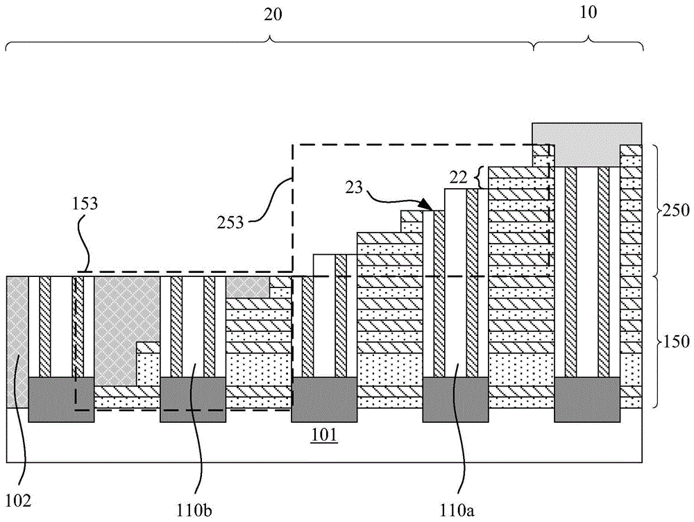
如图3k所示,在形成第二台阶结构253之后,最终的第一虚拟沟道柱110a的至少部分位于第二台阶结构253中,并且至少一个第一虚拟沟道柱110a的顶面23为第二台阶结构253的台阶面。其中,在一些情况下,第一虚拟沟道柱110a的顶面23是同一个台阶22的坡顶面或坡底面。在另一些情况下,第一虚拟沟道柱110a的顶面23部分作为台阶22的坡顶面,另一部分作为相同台阶22的坡底面,两个部分顶面23相连的侧面为相同台阶22的坡面。第一填充层102上方的第二叠层结构250与第二虚拟沟道柱110b均被去除,至少一个第二虚拟沟道柱110b自第一填充层102向衬底101方向延伸,最终的第二虚拟沟道柱110b的至少部分位于第一台阶结构153中,第一台阶结构153在平行于衬底101的方向上突出于第二台阶结构253。As shown in FIG. 3k, after forming the second stepped
进一步的,形成覆盖停止层210、第二叠层结构250以及第一填充结构102的第二填充层205,如图3l所示。在该步骤中,例如采用CVD工艺、PVD工艺沉积TEOS材料形成第二填充层205。进一步的,例如在第二填充层205的表面上形成光刻掩模,然后进行各向异性蚀刻,暴露位于核心区10的停止层210,如图3l所示。Further, a
各向异性蚀刻可以采用干法蚀刻,如离子铣蚀刻、等离子蚀刻、反应离子蚀刻、激光烧蚀。例如,通过控制蚀刻时间,使得蚀刻在到停止层210表面附近停止,以暴露对应的停止层210。在蚀刻之后通过在溶剂中溶解或灰化去除光刻掩模,其中,停止层210作为后续研磨步骤的停止标记。Anisotropic etching can be performed by dry etching, such as ion milling etching, plasma etching, reactive ion etching, and laser ablation. For example, by controlling the etching time, the etching stops near the surface of the
在该步骤中,与常规工艺的不同之处在于,省去了在第二填充层205的表面形成氮化硅停止层这一工艺步骤,也避免了在常规工艺中光刻胶在氮化硅停止层上残留的问题。In this step, the difference from the conventional process is that the process step of forming a silicon nitride stop layer on the surface of the
进一步的,对第二填充层205进行初次平坦化处理,如图3m所示。Further, a primary planarization treatment is performed on the
在该步骤中,例如采用CMP工艺研磨第二填充层205,通过控制时间,使得研磨在到达停止层210附近时停止。In this step, for example, the
进一步的,去除位于核心区10的停止层的一部分,并保留插塞结构211,如图3n所示。Further, a part of the stop layer located in the
在该步骤中,例如采用湿法或干法刻蚀去除插塞结构211上方的停止层,通过控制蚀刻时间,使得蚀刻在到达插塞结构211表面附近停止。In this step, for example, wet or dry etching is used to remove the stop layer above the
进一步的,对第二填充层205进行二次平坦化处理,如图3o所示。Further, a second planarization treatment is performed on the
在该步骤中,例如采用CMP的方法研磨第二填充层205,通过控制时间,使得研磨在到达插塞结构211表面时停止。In this step, for example, the
进一步的,将牺牲层替换为栅极导体层形成3D存储器件。Further, the sacrificial layer is replaced by a gate conductor layer to form a 3D memory device.
如图3a至图3o所示,该3D存储器件包括:衬底101、第一叠层结构150、第一填充层102、第二叠层结构250、第二填充层205以及多个第一虚拟沟道柱110a、多个第二虚拟沟道柱110b以及多个存储沟道柱110c。As shown in FIGS. 3a to 3o, the 3D memory device includes: a
第一叠层结构150位于衬底101上,包括交替堆叠的多个层间绝缘层与栅极导体层,第一叠层结构150具有第一台阶结构153。第一填充层102覆盖第一台阶结构153与衬底101。第二叠层结构250覆盖第一叠层结构150与第一填充层102,包括交替堆叠的多个层间绝缘层与栅极导体层,第二叠层结构250具有第二台阶结构253。第二填充层205覆盖第二台阶结构253与第一填充层102。位于核心区10的存储沟道柱110c贯穿第一叠层结构150与第二叠层结构250。位于台阶区20的第一虚拟沟道柱110a的至少部分位于第二台阶结构253中,至少一个第一虚拟沟道柱110a的顶面为第二台阶结构253的台阶面。位于台阶区20的第二虚拟沟道柱110b自第一填充层102向衬底101方向延伸,第二虚拟沟道柱110b的至少部分位于第一台阶结构153中。插塞结构211位于存储沟道柱110c上,第二填充层205的表面与插塞结构211的表面平齐。The first
在本实施例中,插塞结构211的材料包括多晶硅,第一填充层102与第二填充层205的材料包括正硅酸乙酯。In this embodiment, the material of the
图4a与图4b示出了本发明实施例的效果分析示意图,其中,图4a为用常规工艺制造的3D存储器件的顶视图,图4b示出了沿图4a的截面图。Fig. 4a and Fig. 4b are schematic diagrams showing the effect analysis of the embodiment of the present invention, wherein Fig. 4a is a top view of a 3D memory device manufactured by a conventional process, and Fig. 4b is a cross-sectional view along Fig. 4a.
如图4a与图4b所示,在常规的3D存储器件的制造工艺中,需要先刻蚀第二叠层结构420形成第二台阶结构,覆盖第二台阶结构形成TEOS填充层403,然后再刻蚀第二叠层结构420形成沟道孔,由于填充层403与第二叠层结构420的材料不同,需要在刻蚀沟道孔之前进行退火工艺释放应力,这样就会造成填充层403的形变,位于第一叠层结构320与第二叠层结构420接触部位401的沟道孔不能对准,在形成沟道柱时,会因刻蚀工艺损坏半导体层402,严重影响了器件的良率。As shown in Figure 4a and Figure 4b, in the conventional 3D memory device manufacturing process, it is necessary to etch the second
而本发明实施例在贯穿第二叠层结构形成沟道孔时,牺牲结构完全被第二叠层结构覆盖,仅需要刻蚀第二叠层结构就可以形成沟道孔,由于第二叠层结构应力均匀,不需要在形成沟道孔之前进行退火,防止了由于退火造成第一叠层结构与第一填充层的形变问题,从而使得沟道孔与牺牲结构可以容易地对准。However, in the embodiment of the present invention, when the channel hole is formed through the second stacked structure, the sacrificial structure is completely covered by the second stacked structure, and only the second stacked structure needs to be etched to form the channel hole. The structural stress is uniform, and annealing is not required before forming the channel hole, which prevents the deformation of the first stacked structure and the first filling layer due to annealing, so that the channel hole and the sacrificial structure can be easily aligned.
此外,由于牺牲结构完全被第二叠层结构覆盖,形成沟道孔时不需要刻蚀除第二叠层结构以外的材料(例如常规工艺中台阶区的填充层),降低了刻蚀难度,节省了刻蚀成本。In addition, since the sacrificial structure is completely covered by the second stacked structure, there is no need to etch materials other than the second stacked structure (such as the filling layer of the step region in the conventional process) when forming the channel hole, which reduces the difficulty of etching. The etching cost is saved.
进一步的,在形成第二台阶结构时,将对应部分的沟道柱的形貌制作成与第二台阶结构相同的,在覆盖第二台阶结构与第一填充结构形成第二填充层时,第二填充层中没有其他结构,使得第二填充层的结构完整,分布均匀,在后续研磨过程中,仅需要对第二填充层进行研磨,更容易对研磨的相关工艺参数进行控制。Further, when forming the second stepped structure, the shape of the corresponding part of the channel column is made to be the same as that of the second stepped structure, and when the second filled layer is formed covering the second stepped structure and the first filled structure, the second There is no other structure in the second filling layer, so that the structure of the second filling layer is complete and evenly distributed. In the subsequent grinding process, only the second filling layer needs to be ground, which makes it easier to control the relevant process parameters of grinding.
进一步的,通过覆盖第二叠层结构形成停止层,并将位于接触孔中的停止层复用作为每个沟道柱的插塞结构,在对第二填充层进行初步平坦化处理时,停止层的表面可以作为研磨的停止标记,在对第二填充层进行二次平坦化处理时,插塞结构的表面可以作为研磨的停止标记,由于在本实施中,已经通过同一停止层形成了两次研磨的停止标记,不再需要常规研磨工艺中的位于第二填充层表面的氮化硅停止层作为停止标记,节省了形成氮化硅停止层的工艺步骤,也避免了在常规工艺中光刻胶在氮化硅停止层上残留的问题。Further, the stop layer is formed by covering the second stacked structure, and the stop layer located in the contact hole is reused as the plug structure of each channel column. When the second filling layer is initially planarized, the stop layer The surface of the plug structure can be used as a grinding stop mark. When the second filling layer is planarized, the surface of the plug structure can be used as a grinding stop mark. The stop mark of the secondary grinding does not need the silicon nitride stop layer on the surface of the second filling layer in the conventional grinding process as the stop mark, which saves the process steps of forming the silicon nitride stop layer and also avoids the need for light in the conventional process. The problem of resist residue on the silicon nitride stop layer.
进一步的,在去除位于台阶区的停止层时,通过将同一个光刻掩模的图案分别转移到停止层和靠近停止层的层间绝缘层与牺牲层上,不仅利用保留的停止层作为在对第二填充层进行初次平坦化处理时的研磨停止标记,同时通过刻蚀靠近停止层的层间绝缘层与牺牲层形成了顶部的第二台阶结构,从而省去了用于顶部的第二台阶结构的光刻修饰(trim)步骤。Further, when removing the stop layer located in the step region, by transferring the pattern of the same photolithography mask to the stop layer and the interlayer insulating layer and the sacrificial layer near the stop layer, not only the remaining stop layer is used as the The grinding stop mark when performing the first planarization process on the second filling layer, and at the same time, the second step structure at the top is formed by etching the interlayer insulating layer and the sacrificial layer close to the stop layer, thereby eliminating the need for the second step structure for the top. Photolithographic trimming (trim) step of the stepped structure.
因此,根据本发明实施例的半导体器件及其制造方法提高了产品良率和可靠性。Therefore, the semiconductor device and the manufacturing method thereof according to the embodiments of the present invention improve product yield and reliability.
在以上的描述中,对于各层的构图、蚀刻等技术细节并没有做出详细的说明。但是本领域技术人员应当理解,可以通过各种技术手段,来形成所需形状的层、区域等。另外,为了形成同一结构,本领域技术人员还可以设计出与以上描述的方法并不完全相同的方法。另外,尽管在以上分别描述了各实施例,但是这并不意味着各个实施例中的措施不能有利地结合使用。In the above description, technical details such as patterning and etching of each layer are not described in detail. However, those skilled in the art should understand that various technical means can be used to form layers, regions, etc. of desired shapes. In addition, in order to form the same structure, those skilled in the art can also design a method that is not exactly the same as the method described above. In addition, although the various embodiments are described above separately, this does not mean that the measures in the various embodiments cannot be advantageously used in combination.
以上对本发明的实施例进行了描述。但是,这些实施例仅仅是为了说明的目的,而并非为了限制本发明的范围。本发明的范围由所附权利要求及其等价物限定。不脱离本发明的范围,本领域技术人员可以做出多种替代和修改,这些替代和修改都应落在本发明的范围之内。The embodiments of the present invention have been described above. However, these examples are for illustrative purposes only and are not intended to limit the scope of the present invention. The scope of the invention is defined by the appended claims and their equivalents. Those skilled in the art can make various substitutions and modifications without departing from the scope of the present invention, and these substitutions and modifications should all fall within the scope of the present invention.
Claims (17)
Priority Applications (1)
| Application Number | Priority Date | Filing Date | Title |
|---|---|---|---|
| CN202010001944.6A CN111180454B (en) | 2020-01-02 | 2020-01-02 | 3D memory device and method of manufacturing the same |
Applications Claiming Priority (1)
| Application Number | Priority Date | Filing Date | Title |
|---|---|---|---|
| CN202010001944.6A CN111180454B (en) | 2020-01-02 | 2020-01-02 | 3D memory device and method of manufacturing the same |
Publications (2)
| Publication Number | Publication Date |
|---|---|
| CN111180454A CN111180454A (en) | 2020-05-19 |
| CN111180454B true CN111180454B (en) | 2023-01-20 |
Family
ID=70649297
Family Applications (1)
| Application Number | Title | Priority Date | Filing Date |
|---|---|---|---|
| CN202010001944.6A Active CN111180454B (en) | 2020-01-02 | 2020-01-02 | 3D memory device and method of manufacturing the same |
Country Status (1)
| Country | Link |
|---|---|
| CN (1) | CN111180454B (en) |
Families Citing this family (7)
| Publication number | Priority date | Publication date | Assignee | Title |
|---|---|---|---|---|
| CN114424325B (en) * | 2019-08-07 | 2025-12-05 | 应用材料公司 | Modified stacking for 3D NAND |
| CN111799273A (en) * | 2020-06-11 | 2020-10-20 | 长江存储科技有限责任公司 | A kind of semiconductor device and its manufacturing method |
| CN111952317B (en) * | 2020-08-04 | 2024-04-09 | 长江存储科技有限责任公司 | Three-dimensional memory and preparation method thereof |
| CN112018122B (en) * | 2020-09-08 | 2024-06-11 | 长江存储科技有限责任公司 | Method for forming channel hole of three-dimensional memory device and three-dimensional memory device |
| CN112289804B (en) * | 2020-10-26 | 2021-11-16 | 长江存储科技有限责任公司 | Method for manufacturing 3D memory device |
| CN112951840B (en) * | 2021-02-23 | 2023-04-18 | 长江存储科技有限责任公司 | Three-dimensional memory and preparation method thereof |
| CN119095376B (en) * | 2023-05-29 | 2025-10-03 | 长鑫存储技术有限公司 | Semiconductor device and method for manufacturing the same |
Family Cites Families (3)
| Publication number | Priority date | Publication date | Assignee | Title |
|---|---|---|---|---|
| US9627403B2 (en) * | 2015-04-30 | 2017-04-18 | Sandisk Technologies Llc | Multilevel memory stack structure employing support pillar structures |
| CN106409769A (en) * | 2016-07-04 | 2017-02-15 | 武汉新芯集成电路制造有限公司 | Method for forming storage stack with trapezoidal structures |
| CN109148459B (en) * | 2018-08-07 | 2021-12-03 | 长江存储科技有限责任公司 | 3D memory device and method of manufacturing the same |
-
2020
- 2020-01-02 CN CN202010001944.6A patent/CN111180454B/en active Active
Also Published As
| Publication number | Publication date |
|---|---|
| CN111180454A (en) | 2020-05-19 |
Similar Documents
| Publication | Publication Date | Title |
|---|---|---|
| CN111180454B (en) | 3D memory device and method of manufacturing the same | |
| US9960181B1 (en) | Three-dimensional memory device having contact via structures in overlapped terrace region and method of making thereof | |
| US10269620B2 (en) | Multi-tier memory device with through-stack peripheral contact via structures and method of making thereof | |
| US8089120B2 (en) | Semiconductor memory device | |
| KR101834930B1 (en) | Vertical structure non-volatile memory device | |
| CN109037227B (en) | 3D memory device and method of manufacturing the same | |
| CN110233153B (en) | 3D memory device and method of manufacturing the same | |
| CN111199976B (en) | 3D memory device and manufacturing method thereof | |
| CN110349966B (en) | Manufacturing method of 3D memory device and 3D memory device | |
| US20170345843A1 (en) | Vertical memory devices | |
| CN109390348B (en) | 3D memory device and method of manufacturing the same | |
| TW202027261A (en) | Crenellated charge storage structures for 3d nand | |
| TWI750678B (en) | Semiconductor memory structure and manufacturing method thereof | |
| US7960844B2 (en) | 3-dimensional flash memory device, method of fabrication and method of operation | |
| CN111326526B (en) | 3D memory device and manufacturing method thereof | |
| CN111223870B (en) | 3D memory device and method of manufacturing the same | |
| US20150179575A1 (en) | 3-D IC Device with Enhanced Contact Area | |
| CN111211130B (en) | 3D memory device and method of manufacturing the same | |
| US20120205805A1 (en) | Semiconductor device and method of manufacturing the same | |
| CN111785728B (en) | Method for manufacturing bit line of 3D memory device | |
| CN108847413B (en) | 3D memory devices | |
| CN111211131B (en) | 3D memory device and manufacturing method thereof | |
| CN110277407A (en) | 3D memory device and its manufacturing method | |
| KR20190005574A (en) | Semiconductor devices | |
| CN111180458B (en) | 3D memory device and method of manufacturing the same |
Legal Events
| Date | Code | Title | Description |
|---|---|---|---|
| PB01 | Publication | ||
| PB01 | Publication | ||
| SE01 | Entry into force of request for substantive examination | ||
| SE01 | Entry into force of request for substantive examination | ||
| GR01 | Patent grant | ||
| GR01 | Patent grant |