CN110873910A - Metamaterial-based reflectors, optical cavity structures, and vertical-cavity surface-emitting lasers - Google Patents
Metamaterial-based reflectors, optical cavity structures, and vertical-cavity surface-emitting lasers Download PDFInfo
- Publication number
- CN110873910A CN110873910A CN201910643478.9A CN201910643478A CN110873910A CN 110873910 A CN110873910 A CN 110873910A CN 201910643478 A CN201910643478 A CN 201910643478A CN 110873910 A CN110873910 A CN 110873910A
- Authority
- CN
- China
- Prior art keywords
- metamaterial
- nanostructures
- layer
- reflector
- based reflector
- Prior art date
- Legal status (The legal status is an assumption and is not a legal conclusion. Google has not performed a legal analysis and makes no representation as to the accuracy of the status listed.)
- Granted
Links
Images


Classifications
-
- H—ELECTRICITY
- H01—ELECTRIC ELEMENTS
- H01S—DEVICES USING THE PROCESS OF LIGHT AMPLIFICATION BY STIMULATED EMISSION OF RADIATION [LASER] TO AMPLIFY OR GENERATE LIGHT; DEVICES USING STIMULATED EMISSION OF ELECTROMAGNETIC RADIATION IN WAVE RANGES OTHER THAN OPTICAL
- H01S5/00—Semiconductor lasers
- H01S5/10—Construction or shape of the optical resonator, e.g. extended or external cavity, coupled cavities, bent-guide, varying width, thickness or composition of the active region
- H01S5/18—Surface-emitting [SE] lasers, e.g. having both horizontal and vertical cavities
- H01S5/183—Surface-emitting [SE] lasers, e.g. having both horizontal and vertical cavities having only vertical cavities, e.g. vertical cavity surface-emitting lasers [VCSEL]
- H01S5/18361—Structure of the reflectors, e.g. hybrid mirrors
-
- G—PHYSICS
- G02—OPTICS
- G02B—OPTICAL ELEMENTS, SYSTEMS OR APPARATUS
- G02B5/00—Optical elements other than lenses
- G02B5/30—Polarising elements
- G02B5/3025—Polarisers, i.e. arrangements capable of producing a definite output polarisation state from an unpolarised input state
- G02B5/3058—Polarisers, i.e. arrangements capable of producing a definite output polarisation state from an unpolarised input state comprising electrically conductive elements, e.g. wire grids, conductive particles
-
- G—PHYSICS
- G02—OPTICS
- G02B—OPTICAL ELEMENTS, SYSTEMS OR APPARATUS
- G02B5/00—Optical elements other than lenses
- G02B5/08—Mirrors
-
- G—PHYSICS
- G02—OPTICS
- G02B—OPTICAL ELEMENTS, SYSTEMS OR APPARATUS
- G02B1/00—Optical elements characterised by the material of which they are made; Optical coatings for optical elements
- G02B1/002—Optical elements characterised by the material of which they are made; Optical coatings for optical elements made of materials engineered to provide properties not available in nature, e.g. metamaterials
-
- G—PHYSICS
- G02—OPTICS
- G02B—OPTICAL ELEMENTS, SYSTEMS OR APPARATUS
- G02B5/00—Optical elements other than lenses
- G02B5/18—Diffraction gratings
- G02B5/1809—Diffraction gratings with pitch less than or comparable to the wavelength
-
- H—ELECTRICITY
- H01—ELECTRIC ELEMENTS
- H01S—DEVICES USING THE PROCESS OF LIGHT AMPLIFICATION BY STIMULATED EMISSION OF RADIATION [LASER] TO AMPLIFY OR GENERATE LIGHT; DEVICES USING STIMULATED EMISSION OF ELECTROMAGNETIC RADIATION IN WAVE RANGES OTHER THAN OPTICAL
- H01S5/00—Semiconductor lasers
- H01S5/10—Construction or shape of the optical resonator, e.g. extended or external cavity, coupled cavities, bent-guide, varying width, thickness or composition of the active region
- H01S5/18—Surface-emitting [SE] lasers, e.g. having both horizontal and vertical cavities
- H01S5/183—Surface-emitting [SE] lasers, e.g. having both horizontal and vertical cavities having only vertical cavities, e.g. vertical cavity surface-emitting lasers [VCSEL]
- H01S5/18308—Surface-emitting [SE] lasers, e.g. having both horizontal and vertical cavities having only vertical cavities, e.g. vertical cavity surface-emitting lasers [VCSEL] having a special structure for lateral current or light confinement
- H01S5/18319—Surface-emitting [SE] lasers, e.g. having both horizontal and vertical cavities having only vertical cavities, e.g. vertical cavity surface-emitting lasers [VCSEL] having a special structure for lateral current or light confinement comprising a periodical structure in lateral directions
-
- H—ELECTRICITY
- H01—ELECTRIC ELEMENTS
- H01S—DEVICES USING THE PROCESS OF LIGHT AMPLIFICATION BY STIMULATED EMISSION OF RADIATION [LASER] TO AMPLIFY OR GENERATE LIGHT; DEVICES USING STIMULATED EMISSION OF ELECTROMAGNETIC RADIATION IN WAVE RANGES OTHER THAN OPTICAL
- H01S5/00—Semiconductor lasers
- H01S5/10—Construction or shape of the optical resonator, e.g. extended or external cavity, coupled cavities, bent-guide, varying width, thickness or composition of the active region
- H01S5/18—Surface-emitting [SE] lasers, e.g. having both horizontal and vertical cavities
- H01S5/183—Surface-emitting [SE] lasers, e.g. having both horizontal and vertical cavities having only vertical cavities, e.g. vertical cavity surface-emitting lasers [VCSEL]
- H01S5/18361—Structure of the reflectors, e.g. hybrid mirrors
- H01S5/18369—Structure of the reflectors, e.g. hybrid mirrors based on dielectric materials
-
- H—ELECTRICITY
- H01—ELECTRIC ELEMENTS
- H01S—DEVICES USING THE PROCESS OF LIGHT AMPLIFICATION BY STIMULATED EMISSION OF RADIATION [LASER] TO AMPLIFY OR GENERATE LIGHT; DEVICES USING STIMULATED EMISSION OF ELECTROMAGNETIC RADIATION IN WAVE RANGES OTHER THAN OPTICAL
- H01S5/00—Semiconductor lasers
- H01S5/10—Construction or shape of the optical resonator, e.g. extended or external cavity, coupled cavities, bent-guide, varying width, thickness or composition of the active region
- H01S5/18—Surface-emitting [SE] lasers, e.g. having both horizontal and vertical cavities
- H01S5/183—Surface-emitting [SE] lasers, e.g. having both horizontal and vertical cavities having only vertical cavities, e.g. vertical cavity surface-emitting lasers [VCSEL]
- H01S5/18361—Structure of the reflectors, e.g. hybrid mirrors
- H01S5/18375—Structure of the reflectors, e.g. hybrid mirrors based on metal reflectors
-
- H—ELECTRICITY
- H01—ELECTRIC ELEMENTS
- H01S—DEVICES USING THE PROCESS OF LIGHT AMPLIFICATION BY STIMULATED EMISSION OF RADIATION [LASER] TO AMPLIFY OR GENERATE LIGHT; DEVICES USING STIMULATED EMISSION OF ELECTROMAGNETIC RADIATION IN WAVE RANGES OTHER THAN OPTICAL
- H01S5/00—Semiconductor lasers
- H01S5/10—Construction or shape of the optical resonator, e.g. extended or external cavity, coupled cavities, bent-guide, varying width, thickness or composition of the active region
- H01S5/18—Surface-emitting [SE] lasers, e.g. having both horizontal and vertical cavities
- H01S5/183—Surface-emitting [SE] lasers, e.g. having both horizontal and vertical cavities having only vertical cavities, e.g. vertical cavity surface-emitting lasers [VCSEL]
- H01S5/18361—Structure of the reflectors, e.g. hybrid mirrors
- H01S5/18377—Structure of the reflectors, e.g. hybrid mirrors comprising layers of different kind of materials, e.g. combinations of semiconducting with dielectric or metallic layers
-
- H—ELECTRICITY
- H01—ELECTRIC ELEMENTS
- H01S—DEVICES USING THE PROCESS OF LIGHT AMPLIFICATION BY STIMULATED EMISSION OF RADIATION [LASER] TO AMPLIFY OR GENERATE LIGHT; DEVICES USING STIMULATED EMISSION OF ELECTROMAGNETIC RADIATION IN WAVE RANGES OTHER THAN OPTICAL
- H01S5/00—Semiconductor lasers
- H01S5/10—Construction or shape of the optical resonator, e.g. extended or external cavity, coupled cavities, bent-guide, varying width, thickness or composition of the active region
- H01S5/18—Surface-emitting [SE] lasers, e.g. having both horizontal and vertical cavities
- H01S5/183—Surface-emitting [SE] lasers, e.g. having both horizontal and vertical cavities having only vertical cavities, e.g. vertical cavity surface-emitting lasers [VCSEL]
- H01S5/18386—Details of the emission surface for influencing the near- or far-field, e.g. a grating on the surface
-
- H—ELECTRICITY
- H01—ELECTRIC ELEMENTS
- H01S—DEVICES USING THE PROCESS OF LIGHT AMPLIFICATION BY STIMULATED EMISSION OF RADIATION [LASER] TO AMPLIFY OR GENERATE LIGHT; DEVICES USING STIMULATED EMISSION OF ELECTROMAGNETIC RADIATION IN WAVE RANGES OTHER THAN OPTICAL
- H01S5/00—Semiconductor lasers
- H01S5/10—Construction or shape of the optical resonator, e.g. extended or external cavity, coupled cavities, bent-guide, varying width, thickness or composition of the active region
- H01S5/18—Surface-emitting [SE] lasers, e.g. having both horizontal and vertical cavities
- H01S5/185—Surface-emitting [SE] lasers, e.g. having both horizontal and vertical cavities having only horizontal cavities, e.g. horizontal cavity surface-emitting lasers [HCSEL]
- H01S5/187—Surface-emitting [SE] lasers, e.g. having both horizontal and vertical cavities having only horizontal cavities, e.g. horizontal cavity surface-emitting lasers [HCSEL] using Bragg reflection
-
- G—PHYSICS
- G02—OPTICS
- G02B—OPTICAL ELEMENTS, SYSTEMS OR APPARATUS
- G02B5/00—Optical elements other than lenses
- G02B5/30—Polarising elements
- G02B5/3083—Birefringent or phase retarding elements
-
- H—ELECTRICITY
- H01—ELECTRIC ELEMENTS
- H01S—DEVICES USING THE PROCESS OF LIGHT AMPLIFICATION BY STIMULATED EMISSION OF RADIATION [LASER] TO AMPLIFY OR GENERATE LIGHT; DEVICES USING STIMULATED EMISSION OF ELECTROMAGNETIC RADIATION IN WAVE RANGES OTHER THAN OPTICAL
- H01S5/00—Semiconductor lasers
- H01S5/10—Construction or shape of the optical resonator, e.g. extended or external cavity, coupled cavities, bent-guide, varying width, thickness or composition of the active region
- H01S5/18—Surface-emitting [SE] lasers, e.g. having both horizontal and vertical cavities
- H01S5/183—Surface-emitting [SE] lasers, e.g. having both horizontal and vertical cavities having only vertical cavities, e.g. vertical cavity surface-emitting lasers [VCSEL]
- H01S5/18308—Surface-emitting [SE] lasers, e.g. having both horizontal and vertical cavities having only vertical cavities, e.g. vertical cavity surface-emitting lasers [VCSEL] having a special structure for lateral current or light confinement
- H01S5/18311—Surface-emitting [SE] lasers, e.g. having both horizontal and vertical cavities having only vertical cavities, e.g. vertical cavity surface-emitting lasers [VCSEL] having a special structure for lateral current or light confinement using selective oxidation
-
- H—ELECTRICITY
- H01—ELECTRIC ELEMENTS
- H01S—DEVICES USING THE PROCESS OF LIGHT AMPLIFICATION BY STIMULATED EMISSION OF RADIATION [LASER] TO AMPLIFY OR GENERATE LIGHT; DEVICES USING STIMULATED EMISSION OF ELECTROMAGNETIC RADIATION IN WAVE RANGES OTHER THAN OPTICAL
- H01S5/00—Semiconductor lasers
- H01S5/10—Construction or shape of the optical resonator, e.g. extended or external cavity, coupled cavities, bent-guide, varying width, thickness or composition of the active region
- H01S5/18—Surface-emitting [SE] lasers, e.g. having both horizontal and vertical cavities
- H01S5/183—Surface-emitting [SE] lasers, e.g. having both horizontal and vertical cavities having only vertical cavities, e.g. vertical cavity surface-emitting lasers [VCSEL]
- H01S5/18341—Intra-cavity contacts
-
- H—ELECTRICITY
- H01—ELECTRIC ELEMENTS
- H01S—DEVICES USING THE PROCESS OF LIGHT AMPLIFICATION BY STIMULATED EMISSION OF RADIATION [LASER] TO AMPLIFY OR GENERATE LIGHT; DEVICES USING STIMULATED EMISSION OF ELECTROMAGNETIC RADIATION IN WAVE RANGES OTHER THAN OPTICAL
- H01S5/00—Semiconductor lasers
- H01S5/10—Construction or shape of the optical resonator, e.g. extended or external cavity, coupled cavities, bent-guide, varying width, thickness or composition of the active region
- H01S5/18—Surface-emitting [SE] lasers, e.g. having both horizontal and vertical cavities
- H01S5/183—Surface-emitting [SE] lasers, e.g. having both horizontal and vertical cavities having only vertical cavities, e.g. vertical cavity surface-emitting lasers [VCSEL]
- H01S5/18355—Surface-emitting [SE] lasers, e.g. having both horizontal and vertical cavities having only vertical cavities, e.g. vertical cavity surface-emitting lasers [VCSEL] having a defined polarisation
Landscapes
- Physics & Mathematics (AREA)
- General Physics & Mathematics (AREA)
- Optics & Photonics (AREA)
- Condensed Matter Physics & Semiconductors (AREA)
- Electromagnetism (AREA)
- Optical Elements Other Than Lenses (AREA)
Abstract
Description
相关申请的相交引用CROSS-REFERENCE TO RELATED APPLICATIONS
本申请要求于2018年9月4日向美国专利商标局提交的美国临时专利申请No.61/726,529的优先权,并且要求于2019年1月7日向韩国知识产权局提交的韩国专利申请No.10-2019-0001926的优先权,这两个申请的公开通过全文引用合并于此。This application claims priority to US Provisional Patent Application No. 61/726,529, filed with the United States Patent and Trademark Office on September 4, 2018, and claims Korean Patent Application No. 10, filed with the Korean Intellectual Property Office on January 7, 2019 - Priority to 2019-0001926, the disclosures of both applications are hereby incorporated by reference in their entirety.
技术领域technical field
本公开的示例实施例涉及一种反射器(反射镜)、包括反射器的光学腔结构以及垂直腔表面发射激光器。Example embodiments of the present disclosure relate to a reflector (mirror), an optical cavity structure including the reflector, and a vertical cavity surface emitting laser.
背景技术Background technique
垂直腔表面发射激光器(VCSEL)与边发射激光器(EEL)相比具有较短的光学增益长度,因此可以降低功耗。另外,VCSEL由于垂直发光可以制造成二维阵列,因此有利于高密度集成和大规模生产。虽然根据相关技术的EEL具有不对称的光输出,但是VCSEL提供圆形对称输出模式,使得它们能够高效地连接到光纤并且可以以低噪声进行稳定的高速调制。Vertical-cavity surface-emitting lasers (VCSELs) have shorter optical gain lengths than edge-emitting lasers (EELs), thus reducing power consumption. In addition, VCSELs can be fabricated into two-dimensional arrays due to vertical light emission, which is beneficial for high-density integration and mass production. While EELs according to the related art have asymmetrical light outputs, VCSELs provide circularly symmetric output modes so that they can be efficiently connected to optical fibers and can perform stable high-speed modulation with low noise.
VCSEL配备有:分布式布拉格反射器(DBR),具有约98%或更高的高反射率以构成激光谐振器。由具有不同折射率的两种材料组成的DBR通常需要数十对堆叠结构以便获得高反射率。另外,由于在两种材料之间的边界处发生声子散射,因此DBR具有低导热率(或高热阻)。需要一种能够在补偿DBR的缺点的同时改善光控制和发光特性的技术和方法。The VCSEL is equipped with: Distributed Bragg Reflector (DBR) with a high reflectivity of about 98% or more to constitute a laser resonator. DBRs composed of two materials with different refractive indices typically require dozens of pairs of stacked structures in order to obtain high reflectivity. Additionally, DBR has low thermal conductivity (or high thermal resistance) due to phonon scattering that occurs at the boundary between the two materials. There is a need for a technique and method that can improve light control and light emission characteristics while compensating for the shortcomings of DBR.
发明内容SUMMARY OF THE INVENTION
一个或多个示例实施例提供了一种使用纳米结构的阵列的基于超材料的反射器。One or more example embodiments provide a metamaterial-based reflector using an array of nanostructures.
此外,一个或多个示例实施例提供了一种基于超材料的反射器,其能够容易地控制诸如偏振和会聚/发散之类的光特性。Furthermore, one or more example embodiments provide a metamaterial-based reflector that can easily control light properties such as polarization and convergence/divergence.
此外,一个或多个示例实施例提供了一种应用基于超材料的反射器的光学腔结构和垂直腔表面发射激光器(VCSEL)。Furthermore, one or more example embodiments provide an optical cavity structure and a vertical cavity surface emitting laser (VCSEL) employing a metamaterial-based reflector.
附加方面部分地将在接下来的描述中阐述,且部分地将通过该描述而变得清楚明白,或者可以通过对示例实施例的实践来获知。Additional aspects will be set forth in the description that follows, and in part will be apparent from the description, or may be learned by practice of example embodiments.
根据示例实施例的一方面,提供了一种基于超材料的反射器,包括:第一超材料层,包括第一纳米结构的阵列;以及设置在所述第一超材料层上的第二超材料层,所述第二超材料层包括第二纳米结构的阵列,其中,所述第二纳米结构与所述第一纳米结构不同地布置。According to an aspect of example embodiments, there is provided a metamaterial-based reflector comprising: a first metamaterial layer including an array of first nanostructures; and a second metamaterial disposed on the first metamaterial layer A layer of material, the second metamaterial layer comprising an array of second nanostructures, wherein the second nanostructures are arranged differently from the first nanostructures.
所述第一纳米结构可以沿第一方向并以第一图案布置,并且所述第二纳米结构可以沿与所述第一方向不同的第二方向并且以与所述第一图案不同的第二图案布置。The first nanostructures may be arranged in a first direction and in a first pattern, and the second nanostructures may be arranged in a second direction different from the first direction and in a second direction different from the first pattern pattern arrangement.
所述第一纳米结构可以沿第一方向彼此平行布置,并且所述第二纳米结构可以基于所述第二超材料层的区域,沿与所述第一方向不同的第二方向或者沿与所述第一方向不同的多个方向布置。The first nanostructures may be arranged parallel to each other along a first direction, and the second nanostructures may be based on regions of the second metamaterial layer, along a second direction different from the first direction or along a different direction from the first direction. The first direction is different from a plurality of directions arranged.
所述第一超材料层可以包括透射式波片,所述第二超材料层可以包括反射式波片。The first metamaterial layer may include a transmissive waveplate, and the second metamaterial layer may include a reflective waveplate.
所述第一纳米结构可以沿第一方向彼此平行布置,并且所述第二纳米结构可以沿相对于所述第一方向旋转θ的第二方向彼此平行布置,θ小于90度。The first nanostructures may be arranged parallel to each other along a first direction, and the second nanostructures may be arranged parallel to each other along a second direction rotated with respect to the first direction by θ, where θ is less than 90 degrees.
所述第一纳米结构可以沿第一方向彼此平行布置,并且所述第二纳米结构可以沿相对于所述第一方向旋转的多个方向布置,并且所述第二纳米结构的旋转角度基于所述第二超材料层的区域而不同。The first nanostructures may be arranged parallel to each other in a first direction, and the second nanostructures may be arranged in a plurality of directions rotated with respect to the first direction, and the rotation angles of the second nanostructures are based on the The region of the second metamaterial layer is different.
所述基于超材料的反射器可以被配置为使透射通过所述基于超材料的反射器的光发生圆偏振。The metamaterial-based reflector may be configured to circularly polarize light transmitted through the metamaterial-based reflector.
所述第二纳米结构可以被布置为使得所述基于超材料的反射器操作为会聚镜或发散镜。The second nanostructures may be arranged such that the metamaterial-based reflector operates as a converging mirror or a diverging mirror.
所述第一超材料层可以包括第一透射式波片,所述第二超材料层包括第二透射式波片,并且所述基于超材料的反射器还可以包括与所述第一超材料层相对地设置在所述第二超材料层上的分布式布拉格反射器。The first metamaterial layer may include a first transmissive waveplate, the second metamaterial layer may include a second transmissive waveplate, and the metamaterial-based reflector may further include a combination with the first metamaterial. The layer is disposed opposite the distributed Bragg reflector on the second metamaterial layer.
所述第一纳米结构可以沿第一方向彼此平行布置,并且所述第二纳米结构可以沿相对于所述第一方向旋转θ的第二方向彼此平行布置,θ小于90度。The first nanostructures may be arranged parallel to each other along a first direction, and the second nanostructures may be arranged parallel to each other along a second direction rotated with respect to the first direction by θ, where θ is less than 90 degrees.
所述第一纳米结构可以沿第一方向彼此平行布置,并且所述第二纳米结构可以沿相对于所述第一方向旋转的多个方向布置,并且所述第二纳米结构的旋转角度基于所述第二超材料层的区域而不同。The first nanostructures may be arranged parallel to each other in a first direction, and the second nanostructures may be arranged in a plurality of directions rotated with respect to the first direction, and the rotation angles of the second nanostructures are based on the The region of the second metamaterial layer is different.
所述基于超材料的反射器可以被配置为使透射通过所述基于超材料的反射器的光发生线偏振。The metamaterial-based reflector may be configured to linearly polarize light transmitted through the metamaterial-based reflector.
所述第二纳米结构可以被布置为使得所述基于超材料的反射器被配置为操作为会聚镜或发散镜。The second nanostructure may be arranged such that the metamaterial-based reflector is configured to operate as a converging mirror or a diverging mirror.
根据示例实施例的另一方面,提供了一种光学器件,包括:至少一个基于超材料的反射器,其中,所述至少一个基于超材料的反射器包括第一超材料层,包括第一纳米结构的阵列;以及设置在所述第一超材料层上的第二超材料层,所述第二超材料层包括第二纳米结构的阵列,其中,所述第二纳米结构与所述第一纳米结构不同地布置。According to another aspect of example embodiments, there is provided an optical device comprising: at least one metamaterial-based reflector, wherein the at least one metamaterial-based reflector includes a first metamaterial layer including a first nanomaterial an array of structures; and a second metamaterial layer disposed on the first metamaterial layer, the second metamaterial layer comprising an array of second nanostructures, wherein the second nanostructures are associated with the first The nanostructures are arranged differently.
根据示例实施例的另一方面,提供了一种光学腔结构,包括:增益层,被配置为产生光;第一分布式布拉格反射器,设置在所述增益层的第一表面上;以及基于超材料的反射器,设置在所述增益层的与所述第一分布式布拉格反射器相对的第二表面上,其中,所述基于超材料的反射器包括:第一超材料层,包括第一纳米结构的阵列;以及设置在所述第一超材料层上的第二超材料层,所述第二超材料层包括第二纳米结构的阵列,其中,所述第二纳米结构与所述第一纳米结构不同地布置。According to another aspect of example embodiments, there is provided an optical cavity structure comprising: a gain layer configured to generate light; a first distributed Bragg reflector disposed on a first surface of the gain layer; and based on A metamaterial reflector disposed on a second surface of the gain layer opposite to the first distributed Bragg reflector, wherein the metamaterial-based reflector includes: a first metamaterial layer including a first metamaterial layer an array of nanostructures; and a second metamaterial layer disposed on the first metamaterial layer, the second metamaterial layer comprising an array of second nanostructures, wherein the second nanostructures and the The first nanostructures are arranged differently.
所述第一纳米结构可以沿第一方向彼此平行布置,并且所述第二纳米结构可以基于所述第二超材料层的区域沿与所述第一方向不同的第二方向彼此平行布置,或者沿从所述第一方向旋转的多个方向布置。The first nanostructures may be arranged parallel to each other along a first direction, and the second nanostructures may be arranged parallel to each other along a second direction different from the first direction based on regions of the second metamaterial layer, or Arranged in a plurality of directions rotated from the first direction.
所述第一纳米结构可以沿第一方向彼此平行布置,并且所述第二纳米结构可以沿相对于所述第一方向旋转θ的第二方向彼此平行布置,θ小于90度。The first nanostructures may be arranged parallel to each other along a first direction, and the second nanostructures may be arranged parallel to each other along a second direction rotated with respect to the first direction by θ, where θ is less than 90 degrees.
所述第一纳米结构可以沿第一方向彼此平行布置,并且所述第二纳米结构可以沿相对于所述第一方向旋转的多个方向布置,并且所述第二纳米结构的旋转角度基于所述第二超材料层的区域而不同。The first nanostructures may be arranged parallel to each other in a first direction, and the second nanostructures may be arranged in a plurality of directions rotated with respect to the first direction, and the rotation angles of the second nanostructures are based on the The region of the second metamaterial layer is different.
所述第一超材料层可以包括透射式波片,所述第二超材料层可以包括反射式波片。The first metamaterial layer may include a transmissive waveplate, and the second metamaterial layer may include a reflective waveplate.
所述第一超材料层可以包括第一透射式波片,所述第二超材料层可以包括第二透射式波片,并且所述基于超材料的反射器还可以包括与所述第一超材料层相对地设置在所述第二超材料层上的分布式布拉格反射器。The first metamaterial layer may include a first transmissive waveplate, the second metamaterial layer may include a second transmissive waveplate, and the metamaterial-based reflector may further include a The material layer is disposed opposite the distributed Bragg reflector on the second metamaterial layer.
所述基于超材料的反射器可以被配置为使透射通过所述基于超材料的反射器的光发生圆偏振。The metamaterial-based reflector may be configured to circularly polarize light transmitted through the metamaterial-based reflector.
所述基于超材料的反射器可以被配置为使透射通过所述基于超材料的反射器的光发生线偏振。The metamaterial-based reflector may be configured to linearly polarize light transmitted through the metamaterial-based reflector.
所述第二纳米结构可以被布置为使得所述基于超材料的反射器被配置为操作为会聚镜或发散镜。The second nanostructure may be arranged such that the metamaterial-based reflector is configured to operate as a converging mirror or a diverging mirror.
根据示例实施例的另一方面,提供了一种包括光学腔结构的垂直腔表面发射激光器,所述光学腔结构包括:增益层,被配置为产生光;分布式布拉格反射器,设置在所述增益层的第一表面上;以及基于超材料的反射器,设置在所述增益层的与所述分布式布拉格反射器相对的第二表面上,其中,所述基于超材料的反射器包括:第一超材料层,包括第一纳米结构的阵列;以及设置在所述第一超材料层上的第二超材料层,所述第二超材料层包括第二纳米结构的阵列,其中,所述第二纳米结构与所述第一纳米结构不同地设置。According to another aspect of example embodiments, there is provided a vertical cavity surface emitting laser comprising an optical cavity structure, the optical cavity structure comprising: a gain layer configured to generate light; a distributed Bragg reflector disposed on the on a first surface of a gain layer; and a metamaterial-based reflector disposed on a second surface of the gain layer opposite the distributed Bragg reflector, wherein the metamaterial-based reflector comprises: a first metamaterial layer including an array of first nanostructures; and a second metamaterial layer disposed on the first metamaterial layer, the second metamaterial layer including an array of second nanostructures, wherein the The second nanostructures are arranged differently from the first nanostructures.
所述光学腔结构还可以包括设置在所述增益层和所述基于超材料的反射器之间的接触层。The optical cavity structure may also include a contact layer disposed between the gain layer and the metamaterial-based reflector.
所述光学腔结构还可以包括设置在所述增益层上的孔径层,所述孔径层被配置为调节光的大小和光的振荡中的至少一项。The optical cavity structure may further include an aperture layer disposed on the gain layer, the aperture layer configured to adjust at least one of the size of the light and the oscillation of the light.
所述光学腔结构还可以包括:第一电极,设置在所述增益层的所述第一表面上;第二电极,设置在所述增益层的所述第二表面上。The optical cavity structure may further include: a first electrode disposed on the first surface of the gain layer; and a second electrode disposed on the second surface of the gain layer.
附图说明Description of drawings
上述和/或其他方面将从结合附图对示例实施例的以下描述中变得清楚明白并且易于理解,其中:The above and/or other aspects will be apparent and readily understood from the following description of example embodiments, taken in conjunction with the accompanying drawings, wherein:
图1A和图1B是根据示例实施例的基于超材料的反射器的截面图;1A and 1B are cross-sectional views of metamaterial-based reflectors according to example embodiments;
图2A是图1A和图1B的第一超材料层中包括的多个第一纳米结构的阵列的平面图,图2B是图1A和图1B的第二超材料层中包括的多个第二纳米结构的阵列的平面图;2A is a plan view of an array of a plurality of first nanostructures included in the first metamaterial layer of FIGS. 1A and 1B , and FIG. 2B is a plurality of second nanostructures included in the second metamaterial layer of FIGS. 1A and 1B a plan view of an array of structures;
图3A和图3B是根据示例实施例的基于超材料的反射器的截面图;3A and 3B are cross-sectional views of metamaterial-based reflectors according to example embodiments;
图4A是图3A和图3B的第一超材料层中包括的多个第一纳米结构的阵列的平面图,图4B是图3A和图3B的第二超材料层中包括的多个第二纳米结构的阵列的平面图;4A is a plan view of an array of a plurality of first nanostructures included in the first metamaterial layer of FIGS. 3A and 3B , and FIG. 4B is a plurality of second nanostructures included in the second metamaterial layer of FIGS. 3A and 3B a plan view of an array of structures;
图5A和图5B是根据示例实施例的基于超材料的反射器的截面图;5A and 5B are cross-sectional views of metamaterial-based reflectors according to example embodiments;
图6A是图5A和图5B的第一超材料层中包括的多个第一纳米结构的阵列的平面图,图6B是图5A和图5B的第二超材料层中包括的多个第二纳米结构的阵列的平面图;6A is a plan view of an array of a plurality of first nanostructures included in the first metamaterial layer of FIGS. 5A and 5B , and FIG. 6B is a plurality of second nanostructures included in the second metamaterial layer of FIGS. 5A and 5B a plan view of an array of structures;
图7A和图7B是根据示例实施例的基于超材料的反射器的截面图;7A and 7B are cross-sectional views of metamaterial-based reflectors according to example embodiments;
图8A是图7A和图7B的第一超材料层中包括的多个第一纳米结构的阵列的平面图,图8B是图7A和图7B的第二超材料层中包括的多个第二纳米结构的阵列的平面图;8A is a plan view of an array of a plurality of first nanostructures included in the first metamaterial layer of FIGS. 7A and 7B , and FIG. 8B is a plurality of second nanostructures included in the second metamaterial layer of FIGS. 7A and 7B a plan view of an array of structures;
图9是根据示例实施例的应用了基于超材料的反射器的光学腔结构的截面图;9 is a cross-sectional view of an optical cavity structure to which a metamaterial-based reflector is applied, according to an example embodiment;
图10是根据示例实施例的应用了基于超材料的反射器的光学腔结构的截面图;10 is a cross-sectional view of an optical cavity structure to which a metamaterial-based reflector is applied, according to an example embodiment;
图11是根据示例实施例的应用了基于超材料的反射器的光学腔结构的截面图;11 is a cross-sectional view of an optical cavity structure to which a metamaterial-based reflector is applied, according to an example embodiment;
图12是根据示例实施例的应用了基于超材料的反射器的光学腔结构的截面图;12 is a cross-sectional view of an optical cavity structure to which a metamaterial-based reflector is applied, according to an example embodiment;
图13是根据示例实施例的包括使用基于超材料的反射器的光学腔结构的垂直腔表面发射激光器(VCSEL)的截面图;13 is a cross-sectional view of a vertical cavity surface emitting laser (VCSEL) including an optical cavity structure using a metamaterial-based reflector, according to an example embodiment;
图14是根据示例实施例的包括使用基于超材料的反射器的光学腔结构的VCSEL的截面图;14 is a cross-sectional view of a VCSEL including an optical cavity structure using a metamaterial-based reflector, according to an example embodiment;
图15A是根据示例实施例的包括使用基于超材料的反射器的光学腔结构的VCSEL的截面图;15A is a cross-sectional view of a VCSEL including an optical cavity structure using a metamaterial-based reflector, according to an example embodiment;
图15B是图15A的VCSEL的分解截面图;Figure 15B is an exploded cross-sectional view of the VCSEL of Figure 15A;
图15C是示出了图15B的超材料层中包括的多个纳米结构的阵列的平面图;Figure 15C is a plan view showing an array of a plurality of nanostructures included in the metamaterial layer of Figure 15B;
图16是示出了图15B的VCSEL的下部子结构的反射率变化和相位变化的图;FIG. 16 is a graph showing reflectivity change and phase change of the lower substructure of the VCSEL of FIG. 15B;
图17A和图17B是示出了图15B的VCSEL的上部结构的反射相位的图;以及Figures 17A and 17B are graphs showing the reflection phase of the upper structure of the VCSEL of Figure 15B; and
图18和图19是示出了根据示例实施例的可以应用于基于超材料的反射器的超材料层的纳米结构的阵列的图像。18 and 19 are images illustrating an array of nanostructures of a metamaterial layer that may be applied to a metamaterial based reflector, according to example embodiments.
具体实施方式Detailed ways
现在详细参考附图中所示的示例实施例,贯穿附图相同的附图标记指代相同的元件。在这点上,示例实施例可以具有不同形式,并且不应当被解释为受限于本文所阐明的描述。因此,下面仅通过参考附图描述示例实施例,以解释各个方面。如本文所用,术语“和/或”包括关联列出的项目中的一个或多个项目的任意和所有组合。诸如“......中的至少一个”之类的表述在元件列表之前时修饰整个元件列表,而不是修饰列表中的单独元件。例如,表述“a、b和c中的至少一个”应该理解为仅包括a、仅包括b、仅包括c、包括a和b两者、包括a和c两者、包括b和c二者、或包括a、b和c的全部。Reference will now be made in detail to example embodiments illustrated in the accompanying drawings, wherein like reference numerals refer to like elements throughout. In this regard, example embodiments may take different forms and should not be construed as limited to the descriptions set forth herein. Accordingly, example embodiments are merely described below, by referring to the figures, to explain various aspects. As used herein, the term "and/or" includes any and all combinations of one or more of the associated listed items. Expressions such as "at least one of" when preceding a list of elements modify the entire list of elements, rather than modifying individual elements of the list. For example, the expression "at least one of a, b and c" should be understood to include a only, b only, c only, both a and b, both a and c, both b and c, Or include all of a, b and c.
在下文中,将参照附图描述根据示例实施例的基于超材料的反射器和包括基于超材料的反射器的光学腔结构以及垂直腔表面发射激光器(VCSEL)。为了说明的清楚和描述的方便起见,附图中所示的层或区域的宽度和厚度可以被夸大。Hereinafter, a metamaterial-based reflector and an optical cavity structure including the metamaterial-based reflector and a vertical cavity surface emitting laser (VCSEL) according to example embodiments will be described with reference to the accompanying drawings. The widths and thicknesses of layers or regions shown in the drawings may be exaggerated for clarity of illustration and convenience of description.
图1A和图1B是根据示例实施例的基于超材料的反射器100A的截面图。图1A示出了入射光的透射特性,图1B示出了反射光的特性。基于超材料的反射器100A可以被称为超表面反射镜或基于纳米结构的反射镜。1A and 1B are cross-sectional views of a metamaterial-based
参照图1A和图1B,基于超材料的反射器100A可以包括第一超材料层M10和第二超材料层M20,第一超材料层M10包括多个第一纳米结构n10的阵列,第二超材料层M20位于第一超材料层M10上并且包括多个第二纳米结构n20的阵列。多个第二纳米结构n20可以与多个第一纳米结构n10不同地布置。多个第二纳米结构n20的布置方向和布置方案可以与多个第一纳米结构n10的布置方向和布置方案不同。例如,多个第一纳米结构n10可以沿第一方向彼此平行地布置,并且多个第二纳米结构n20可以沿与第一方向不同的方向布置。第一超材料层M10可以被称为第一纳米结构阵列层,第二超材料层M20可以被称为第二纳米结构阵列层。第一超材料层M10可以包括第一材料层m10,第二超材料层M20可以包括第二材料层m20。第一材料层m10的折射率可以小于第一纳米结构n10的折射率,并且第二材料层m20的折射率可以小于第二纳米结构n20的折射率。第一材料层m10和第二材料层m20可以分别与多个第一纳米结构n10和多个第二纳米结构n20接触,同时覆盖并包封多个第一纳米结构n10和多个第二纳米结构n20。亦即,第一超材料层M10可以包括多个第一纳米结构n10和覆盖并包封多个第一纳米结构n10的第一材料层m10,第二超材料层M20可以包括多个第二纳米结构n20和覆盖并包封多个第二纳米结构n20的第二材料层m20。第一材料层m10和第二材料层m20可以是电介质或绝缘体。Referring to FIGS. 1A and 1B, a metamaterial-based
在示例实施例中,第一超材料层M10可以是透射式波片,第二超材料层M20可以是反射式波片。例如,第一超材料层M10可以是透射式四分之一波片,第二超材料层M20可以是反射式半波片。在这种情况下,基于超材料的反射器100A可以用作诸如反射镜之类的反射器,而无需单独的反射镜构件。基于超材料的反射器100A可以是双层超表面反射镜。第二超材料层M20可以根据第二纳米结构n20的材料、形状、尺寸、图案间隔等被设计为反射型,并且可以用作反射式半波片。In example embodiments, the first metamaterial layer M10 may be a transmissive waveplate, and the second metamaterial layer M20 may be a reflective waveplate. For example, the first metamaterial layer M10 may be a transmissive quarter-wave plate, and the second metamaterial layer M20 may be a reflective half-wave plate. In this case, the metamaterial-based
参照图1A,基于超材料的反射器100A可以被配置为使得透射通过其的光(例如,透射光L30)发生圆偏振。当入射光L10相对于X轴线偏振+45度时,基于超材料的反射器100A可以使透射光L30发生圆偏振。1A, a metamaterial-based
参照图1B,被基于超材料的反射器100A反射的光(例如,反射光L20)可以保持图1A中的入射光L10的线偏振状态。即,反射光L20可以相对于X轴线偏振+45度。Referring to FIG. 1B , light (eg, reflected light L20 ) reflected by metamaterial-based
图2A是图1A和图1B的第一超材料层M10中包括的多个第一纳米结构n10的阵列的平面图,图2B是图1A和图1B的第二超材料层M20中包括的多个第二纳米结构n20的阵列的平面图。2A is a plan view of an array of a plurality of first nanostructures n10 included in the first metamaterial layer M10 of FIGS. 1A and 1B , and FIG. 2B is a plan view of a plurality of arrays of first nanostructures n10 included in the second metamaterial layer M20 of FIGS. 1A and 1B Plan view of the array of second nanostructures n20.
参照图2A,多个第一纳米结构n10可以沿第一方向(例如,X轴方向)彼此平行布置,并且可以二维布置。Referring to FIG. 2A , the plurality of first nanostructures n10 may be arranged parallel to each other along a first direction (eg, X-axis direction), and may be arranged two-dimensionally.
参照图2B,多个第二纳米结构n20可以沿相对于第一方向旋转θ的第二方向彼此平行布置。θ可以小于90度。Referring to FIG. 2B , a plurality of second nanostructures n20 may be arranged parallel to each other along a second direction rotated by θ with respect to the first direction. θ may be less than 90 degrees.
通过相对于多个第一纳米结构n10的布置方向改变多个第二纳米结构n20的布置方向,包括第一纳米结构n10和第二纳米结构n20的基于超材料的反射器100A可以具有如参考图1A和图1B所述的光学特性。By changing the arrangement direction of the plurality of second nanostructures n20 with respect to the arrangement direction of the plurality of first nanostructures n10, the metamaterial-based
图3A和图3B是根据示例实施例的基于超材料的反射器100B的截面图。图3A示出了入射光的透射特性,图3B示出了反射光的特性。3A and 3B are cross-sectional views of a metamaterial-based
参照图3A和图3B,基于超材料的反射器100B可以包括第一超材料层M11和第二超材料层M21,第一超材料层M11包括多个第一纳米结构n11的阵列,第二超材料层M21位于第一超材料层M11上并且包括多个第二纳米结构n21的阵列。多个第二纳米结构n21可以与多个第一纳米结构n11不同地布置。例如,多个第一纳米结构n11可以沿第一方向彼此平行布置,并且多个第二纳米结构n21的布置方向可以根据第二超材料层M21的区域而改变。第一超材料层M11可以包括第一材料层m11,第二超材料层M21可以包括第二材料层m21。即,第一超材料层M11可以包括多个第一纳米结构n11和覆盖并包封多个第一纳米结构n11的第一材料层m11,第二超材料层M21可以包括多个第二纳米结构n21和覆盖并包封多个第二纳米结构n21的第二材料层m21。3A and 3B, the metamaterial-based
在示例实施例中,第一超材料层M11可以是透射式波片,第二超材料层M21可以是反射式波片。例如,第一超材料层M11可以是透射式四分之一波片,第二超材料层M21可以是反射式半波片。In example embodiments, the first metamaterial layer M11 may be a transmissive waveplate, and the second metamaterial layer M21 may be a reflective waveplate. For example, the first metamaterial layer M11 may be a transmissive quarter-wave plate, and the second metamaterial layer M21 may be a reflective half-wave plate.
根据示例实施例的基于超材料的反射器100B可以用作会聚镜或发散镜。基于基于超材料的反射器100B是用作会聚镜还是发散镜,可以确定多个第二纳米结构n21的布置。The metamaterial-based
参照图3A,基于超材料的反射器100A可以被配置为使得透射通过其的光(例如,透射光L31)发生圆偏振。当入射光L11相对于X轴线偏振+45度时,基于超材料的反射器100B可以使透射光L31发生圆偏振。3A, the metamaterial-based
参照图3B,被基于超材料的反射器100B反射的光(例如,反射光L21)可以保持图3A中的入射光L11的线偏振状态。即,反射光L21可以相对于X轴线偏振+45度。基于超材料的反射器100B可以对于如图3A所示的线偏振+45度的入射光L11用作具有焦距f的会聚镜。为此,多个第二纳米结构n21的布置方向可以根据第二超材料层M21的区域而改变,如下面参考图4B所述。反射光L21可以具有焦距为f的会聚波前。基于超材料的反射器100B可以对于线偏振-45度的入射光用作具有负焦距-f的发散镜。Referring to FIG. 3B , light (eg, reflected light L21 ) reflected by the metamaterial-based
返回参照图3A,对于线偏振+45度的入射光L11,透射光L31可以是具有与焦距f对应的会聚波前的圆偏振光。Referring back to FIG. 3A , for the incident light L11 of linear polarization +45 degrees, the transmitted light L31 may be circularly polarized light having a converging wavefront corresponding to the focal length f.
图4A是图3A和图3B的第一超材料层M11中包括的多个第一纳米结构n11的阵列的平面图,图4B是图3A和图3B的第二超材料层M21中包括的多个第二纳米结构n21的阵列的平面图。4A is a plan view of an array of a plurality of first nanostructures n11 included in the first metamaterial layer M11 of FIGS. 3A and 3B , and FIG. 4B is a plurality of arrays included in the second metamaterial layer M21 of FIGS. 3A and 3B Plan view of the array of second nanostructures n21.
参照图4A,多个第一纳米结构n11可以沿第一方向(例如,X轴方向)彼此平行布置。Referring to FIG. 4A , the plurality of first nanostructures n11 may be arranged in parallel with each other along a first direction (eg, the X-axis direction).
参照图4B,多个第二纳米结构n21可以被布置为相对于第一方向旋转,并且第二纳米结构n21的旋转角度可以根据第二超材料层M21的区域而变化。第二纳米结构n21的旋转角度可以相对于预定点(例如,第二超材料层M21的中心)朝向第二超材料层M21的外周逐渐增大。以这种方式,通过相对于多个第一纳米结构n11的布置方向改变多个第二纳米结构n21的布置方向并且根据第二超材料层M21的区域改变旋转角度,包括第一纳米结构n11和第二纳米结构n21的基于超材料的反射器100B可以具有如参考图3A和图3B所述的光学特性。Referring to FIG. 4B , the plurality of second nanostructures n21 may be arranged to rotate with respect to the first direction, and the rotation angle of the second nanostructures n21 may vary according to the area of the second metamaterial layer M21. The rotation angle of the second nanostructure n21 may gradually increase toward the outer periphery of the second metamaterial layer M21 with respect to a predetermined point (eg, the center of the second metamaterial layer M21). In this way, by changing the arrangement direction of the plurality of second nanostructures n21 with respect to the arrangement direction of the plurality of first nanostructures n11 and changing the rotation angle according to the area of the second metamaterial layer M21, the first nanostructures n11 and The metamaterial-based
如在以上示例实施例中所述,第一超材料层M10和M11可以是透射式波片,第二超材料层M20和M21可以是反射式波片。然而,示例实施例不限于此。根据示例实施例,第一超材料层可以是第一透射式波片,第二超材料层可以是第二透射式波片。这样,当第一超材料层和第二超材料层是透射式波片时,还可以在第二超材料层上设置单独的反射镜构件,例如分布式布拉格反射器(DBR),如图5A至图8B所示。As described in the above example embodiments, the first metamaterial layers M10 and M11 may be transmissive waveplates, and the second metamaterial layers M20 and M21 may be reflective waveplates. However, example embodiments are not limited thereto. According to example embodiments, the first metamaterial layer may be a first transmissive waveplate, and the second metamaterial layer may be a second transmissive waveplate. In this way, when the first metamaterial layer and the second metamaterial layer are transmissive wave plates, a separate mirror member, such as a distributed Bragg reflector (DBR), can also be arranged on the second metamaterial layer, as shown in Figure 5A as shown in Figure 8B.
图5A和图5B是根据示例实施例的基于超材料的反射器100C的截面图。图5A示出了入射光的透射特性,图5B示出了反射光的特性。5A and 5B are cross-sectional views of a metamaterial-based
参照图5A和图5B,基于超材料的反射器100C可以包括第一超材料层M12和第二超材料层M22,第一超材料层M12包括多个第一纳米结构n12的阵列,第二超材料层M21位于第一超材料层M12上并且包括多个第二纳米结构n22的阵列。多个第二纳米结构n22可以与多个第一纳米结构n12不同地布置。例如,多个第一纳米结构n12可以沿第一方向彼此平行地布置,并且多个第二纳米结构n22可以沿与第一方向不同的方向布置。第一超材料层M12可以包括第一材料层m12,第二超材料层M22可以包括第二材料层m22。5A and 5B, the metamaterial-based
在示例实施例中,第一超材料层M12可以是第一透射式波片,第二超材料层M22可以是第二透射式波片。在该示例中,基于超材料的反射器100C还可以包括单独的反射镜构件,例如DBR R12,与第一超材料层M12相对地设置在第二超材料层M22上。第二超材料层M22可以是根据第二纳米结构n22的材料、形状、尺寸、图案间隔等的透射层,并且可以操作为透射式波片。DBR R12可以通过交替地且重复地堆叠具有不同折射率的两个材料层至谐振波长的约1/4的厚度来形成。DBR R12的反射率可以通过控制DBR R12的两个材料层的折射率之间的差异和一对两个材料层重复堆叠的次数来控制。DBR R12可以通过交替地堆叠例如非晶硅(a-Si)和氧化硅(SiO2)来形成。然而,DBR R12的材料不限于此。能够形成折射率差异的各种材料可以用作DBR R12的材料。In example embodiments, the first metamaterial layer M12 may be a first transmissive waveplate, and the second metamaterial layer M22 may be a second transmissive waveplate. In this example, the metamaterial based
参照图5A,基于超材料的反射器100C可以被配置为使得透射通过其的光(例如,透射光L32)线偏振。当入射光L12相对于X轴线偏振+45度时,基于超材料的反射器100C可以使透射光L32线偏振-45度。5A, the metamaterial-based
参照图5B,被基于超材料的反射器100C反射的光(例如,反射光L22)可以保持图5B中的入射光L12的线偏振状态。即,反射光L22可以相对于X轴线偏振+45度。Referring to FIG. 5B , light (eg, reflected light L22 ) reflected by the metamaterial-based
图6A是图5A和图5B的第一超材料层M12中包括的多个第一纳米结构n12的阵列的平面图,图6B是图5A和图5B的第二超材料层M22中包括的多个第二纳米结构n22的阵列的平面图。6A is a plan view of an array of a plurality of first nanostructures n12 included in the first metamaterial layer M12 of FIGS. 5A and 5B , and FIG. 6B is a plan view of a plurality of arrays of first nanostructures n12 included in the second metamaterial layer M22 of FIGS. 5A and 5B Plan view of the array of second nanostructures n22.
参照图6A,多个第一纳米结构n12可以沿第一方向(例如,X轴方向)彼此平行布置。Referring to FIG. 6A , the plurality of first nanostructures n12 may be arranged in parallel with each other along a first direction (eg, the X-axis direction).
参照图6B,多个第二纳米结构n22可以沿相对于第一方向旋转θ的第二方向彼此平行布置。θ可以小于90度。Referring to FIG. 6B , the plurality of second nanostructures n22 may be arranged parallel to each other along a second direction rotated by θ with respect to the first direction. θ may be less than 90 degrees.
通过相对于多个第一纳米结构n12的布置方向改变多个第二纳米结构n22的布置方向,包括第一纳米结构n12和第二纳米结构n22的基于超材料的反射器100C可以具有如参考图5A和图5B所述的光学特性。可以通过调整布置方向,例如相对于第一纳米结构n12的布置方向调整第二纳米结构n22的旋转角度,来控制图5B中的反射光L22的相位。By changing the arrangement direction of the plurality of second nanostructures n22 with respect to the arrangement direction of the plurality of first nanostructures n12, the metamaterial-based
当入射光根据基于超材料的反射器100C的偏振本征态中的任何偏振本征态而偏振时,入射光的偏振可以在入射光穿过第一超材料层M12时变为椭圆偏振。当椭圆偏振光穿过第二超材料层M22时,椭圆偏振光的偏振可以转换为线偏振。例如,当第一超材料层M12用作四分之一波片时,第一超材料层M12和第二超材料层M22之间的光的偏振状态可以是圆形的。When the incident light is polarized according to any of the polarization eigenstates of the metamaterial-based
图7A和图7B是根据示例实施例的基于超材料的反射器100D的截面图。图7A示出了入射光的透射特性,图7B示出了反射光的特性。7A and 7B are cross-sectional views of a metamaterial-based
参照图7A和图7B,基于超材料的反射器100D可以包括第一超材料层M13和第二超材料层M23,第一超材料层M13包括多个第一纳米结构n13的阵列,第二超材料层M23位于第一超材料层M13上并且包括多个第二纳米结构n23的阵列。多个第二纳米结构n23可以与多个第一纳米结构n13不同地布置。例如,多个第一纳米结构n13可以沿第一方向彼此平行布置,并且多个第二纳米结构n23的布置方向可以根据第二超材料层M23的区域而改变。第一超材料层M13可以包括第一材料层m13,第二超材料层M23可以包括第二材料层m23。7A and 7B, the metamaterial-based
在示例实施例中,第一超材料层M13可以是第一透射式波片,第二超材料层M23可以是第二透射式波片。在该示例中,基于超材料的反射器100D还可以包括单独的反射镜构件,例如DBR R13,设置在第二超材料层M23上。In example embodiments, the first metamaterial layer M13 may be a first transmissive waveplate, and the second metamaterial layer M23 may be a second transmissive waveplate. In this example, the metamaterial based
根据示例实施例的基于超材料的反射器100D可以用作会聚镜或发散镜。基于基于超材料的反射器100B是用作会聚镜还是发散镜,可以确定多个第二纳米结构n23的布置。The metamaterial-based
参照图7A,基于超材料的反射器100D可以被配置为使得透射通过其的光(例如,透射光L33)发生圆偏振。当入射光L13相对于X轴线偏振+45度时,透射光L33可以保持线偏振+45度的状态。7A, the metamaterial-based
参照图7B,被基于超材料的反射器100D反射的光(例如,反射光L23)可以保持图7A中的入射光L13的线偏振状态。即,反射光L23可以相对于X轴线偏振+45度。基于超材料的反射器100D可以对于如图7A所示的线偏振+45度的入射光L13用作具有焦距f的会聚镜、聚焦镜。为此,多个第二纳米结构n23的布置方向可以根据第二超材料层M23的区域而改变,如下面参考图8B所述。反射光L23可以具有焦距为f的会聚波前。基于超材料的反射器100D可以对于线偏振-45度的入射光用作具有负焦距-f的发散镜。Referring to FIG. 7B , light (eg, reflected light L23 ) reflected by the metamaterial-based
返回参照图7A,对于线偏振+45度的入射光L13,透射光L33可以是具有与半焦距(即,f/2)对应的会聚波前的线偏振光。Referring back to FIG. 7A , for incident light L13 of linear polarization +45 degrees, transmitted light L33 may be linearly polarized light having a converging wavefront corresponding to a half focal length (ie, f/2).
图8A是图7A和图7B的第一超材料层M13中包括的多个第一纳米结构n13的阵列的平面图,图8B是图7A和图7B的第二超材料层M23中包括的多个第二纳米结构n23的阵列的平面图。8A is a plan view of an array of a plurality of first nanostructures n13 included in the first metamaterial layer M13 of FIGS. 7A and 7B , and FIG. 8B is a plurality of arrays included in the second metamaterial layer M23 of FIGS. 7A and 7B Plan view of the array of second nanostructures n23.
参照图8A,多个第一纳米结构n13可以沿第一方向(例如,X轴方向)彼此平行布置。Referring to FIG. 8A , the plurality of first nanostructures n13 may be arranged in parallel with each other along a first direction (eg, the X-axis direction).
参照图8B,多个第二纳米结构n23可以被布置为相对于第一方向旋转,并且第二纳米结构n23的旋转角度可以根据第二超材料层M23的区域而变化。第二纳米结构n23的旋转角度可以相对于预定点(例如,第二超材料层M23的中心)朝向第二超材料层M23的外周逐渐增加。通过相对于多个第一纳米结构n13的布置方向改变多个第二纳米结构n23的布置方向并且根据第二超材料层M23的区域改变旋转角度,包括第一纳米结构n13和第二纳米结构n23的基于超材料的反射器100D可以具有如参考图7A和图7B所述的光学特性。Referring to FIG. 8B , the plurality of second nanostructures n23 may be arranged to rotate with respect to the first direction, and the rotation angle of the second nanostructures n23 may vary according to the area of the second metamaterial layer M23. The rotation angle of the second nanostructure n23 may gradually increase toward the outer periphery of the second metamaterial layer M23 with respect to a predetermined point (eg, the center of the second metamaterial layer M23). By changing the arrangement direction of the plurality of second nanostructures n23 with respect to the arrangement direction of the plurality of first nanostructures n13 and changing the rotation angle according to the area of the second metamaterial layer M23, the first nanostructure n13 and the second nanostructure n23 are included The metamaterial-based
示例实施例可以实现基于超材料的反射器,可以更容易地控制诸如偏振和会聚/发散之类的光特性。在包括两个超材料层的双层超表面反射镜中,双层超表面反射镜的反射相位可以通过相对于纳米结构(例如,两个超材料层中的一个的超原子)的布置方向旋转纳米结构(例如,两个超材料层中的另一个的超原子)的布置方向来改变。双层超表面反射镜可以用于形成法布里-珀罗谐振腔,并且法布里-珀罗谐振腔的谐振波长可以通过纳米结构(例如,两个超材料层中的一个的超原子)的旋转角度来调节。此外,通过根据区域相对于纳米结构(例如,两个超材料层中的一个的超原子)的布置方向改变纳米结构(例如,两个超材料层中的另一个的超原子)的旋转角度,可以产生会聚镜或发散镜。Example embodiments can implement metamaterial-based reflectors that can more easily control light properties such as polarization and convergence/divergence. In a bilayer metasurface mirror comprising two metamaterial layers, the reflection phase of the bilayer metasurface mirror can be rotated by the orientation of the arrangement relative to the nanostructure (e.g., the metaatoms of one of the two metamaterial layers) The orientation of the nanostructures (eg, the superatoms of the other of the two metamaterial layers) is changed. Two-layer metasurface mirrors can be used to form Fabry-Perot resonators, and the resonant wavelengths of the Fabry-Perot resonators can be passed through nanostructures (e.g., metaatoms in one of the two metamaterial layers) to adjust the rotation angle. Furthermore, by changing the rotation angle of the nanostructures (eg, the superatoms of the other of the two metamaterial layers) according to the orientation of the regions relative to the arrangement of the nanostructures (eg, the superatoms of the other of the two metamaterial layers), Converging or diverging mirrors can be created.
参考图5A至图6B描述的基于超材料的反射器100C中的第一超材料层M12和第二超材料层M22中的每个可以是透射型并且具有双折射特性,因此可以至少部分地用作诸如相位延迟器之类的波片。还可以在第二超材料层M22上设置单独的反射镜构件,例如DBR R12。当第二超材料层M20被设计为反射式时,如图1A至图2B的基于超材料的反射器100A的情况,可以不包括诸如DBR R12之类的单独的反射镜构件。Each of the first metamaterial layer M12 and the second metamaterial layer M22 in the metamaterial-based
当X轴是第一超材料层M12的快轴并且第一超材料层M12与第二超材料层M22的快轴之间的角度是θ时,整个层的琼斯矩阵由下面的方程1给出。When the X axis is the fast axis of the first metamaterial layer M12 and the angle between the fast axis of the first metamaterial layer M12 and the second metamaterial layer M22 is θ, the Jones matrix of the entire layer is given by
[方程1][Equation 1]
T=W(Γ1)R(θ)W(2Γ2)R(-θ)W(Γ1)T=W(Γ 1 )R(θ)W(2Γ 2 )R(-θ)W(Γ 1 )
在方程1中,Γ1表示由第一超材料层M12引起的延迟,Γ2表示由第二超材料层M22引起的延迟,W(Γ)表示具有相位延迟的波片的琼斯矩阵,并且R(θ)表示旋转矩阵。入射光可以依次穿过第一超材料层M12和第二超材料层M22,然后沿相反方向穿过第二超材料层M22,然后再次穿过第一超材料层M12。W(Γ)可以用下面的方程2表示。In
[方程2][Equation 2]
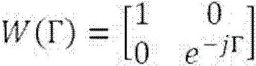
方程2是具有延迟Γ的波片的琼斯矩阵。另外,R(θ)可以用下面的方程3表示。
[方程3][Equation 3]

方程3是旋转矩阵。当第一超材料层M12和第二超材料层M22都用作四分之一波片时,即当Γ1=Γ2=π/2时,T矩阵可以用下面的方程4表示。
[方程4][Equation 4]
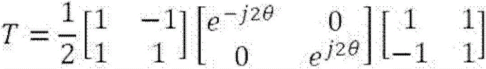
T的两个偏振本征态可以相对于X轴以+/-45度线偏振。这两个偏振的反射相位可以等于+/-2θ,并且可以通过相对于第一超材料层M12的光轴旋转第二超材料层M22的光轴来调整。当第一超材料层M12不是四分之一波片时,即当Γ1≠π/2时,偏振本征态可以是线偏振的,但是可以通过改变θ实现小于2π的相移。The two polarization eigenstates of T can be linearly polarized at +/- 45 degrees relative to the X axis. The reflection phases of these two polarizations can be equal to +/- 2Θ and can be adjusted by rotating the optical axis of the second metamaterial layer M22 relative to the optical axis of the first metamaterial layer M12. When the first metamaterial layer M12 is not a quarter-wave plate, that is, when Γ 1 ≠π/2, the polarization eigenstate can be linearly polarized, but a phase shift of less than 2π can be achieved by changing θ.
相对于图5A和图5B中的基于超材料的反射器100C的X轴线偏振+45度的入射光L12的反射系数可以是e-j2θ。例如,当入射光L12是1时,反射光L22可以是e-j2θ。另外,相对于基于超材料的反射器100C的X轴线偏振-45度的入射光的反射系数也可以是e-j2θ。相对于图1A和图1B中的基于超材料的反射器100A的X轴线偏振+45度或-45度的入射光L10的反射系数也可以是e-j2θ。The reflection coefficient of incident light L12 polarized at +45 degrees relative to the X-axis of the metamaterial-based
在以上示例实施例中,第一纳米结构n10至n13和第二纳米结构n20至n23中的每个可以具有亚波长形状尺寸。亚波长形状尺寸表示作为限定第一纳米结构n10至n13和第二纳米结构n20至n23的形状的尺寸的厚度或宽度小于基于超材料的反射器100A至100D的工作波长。基于超材料的反射器100A至100D的工作波长可以表示振荡波长或谐振波长。第一纳米结构n10至n13和第二纳米结构n20至n23中的每个的厚度、宽度和布置间隔(即,间距)中的至少一个可以小于或等于振荡波长或谐振波长的1/2。In the above example embodiments, each of the first nanostructures n10 to n13 and the second nanostructures n20 to n23 may have subwavelength shape dimensions. The subwavelength shape dimension means that the thickness or width, which is the dimension that defines the shape of the first nanostructures n10 to n13 and the second nanostructures n20 to n23, is less than the operating wavelength of the metamaterial based
第一纳米结构n10至n13和第二纳米结构n20至n23可以包括电介质材料或半导体材料。例如,第一纳米结构n10至n13和第二纳米结构n20至n23可以包括从单晶硅、多晶硅、非晶硅、氮化硅(Si3N4)、磷化镓(GaP)、氧化钛(TiO2)、锑化铝(AlSb)、砷化铝(AlAs)、砷化铝镓(AlGaAs)、磷化铝镓铟(AlGaInP)、磷化硼(BP)和磷化锌锗(ZnGeP2)中选择的任何一种。第一纳米结构n10至n13和第二纳米结构n20至n23可以包括导电材料。作为导电材料,可以采用能够引起表面等离子体激发的高导电金属材料。从铜(Cu)、铝(A1)、镍(Ni)、铁(Fe)、钴(Co)、锌(Zn)、钛(Ti)、钌(Ru)、铑(Rh)、钯(Pd)、铂(Pt)、银(Ag)、锇(Os)、铱(Ir)和金(Au)中选择的至少一种可以用作导电材料,或者包括它们中的任何一种的合金可以用作导电材料。此外,诸如石墨烯或导电氧化物之类的具有良好导电性的二维材料可以用作导电材料。第一纳米结构n10至n13和第二纳米结构n20至n23可以包括III-V族半导体化合物。根据示例实施例,第一纳米结构n10至n13和第二纳米结构n20至n23中的一些可以包括具有相对高折射率的电介质材料,并且第一纳米结构n10至n13和第二纳米结构n20至n23中的一些可以包括导电材料。The first nanostructures n10 to n13 and the second nanostructures n20 to n23 may include a dielectric material or a semiconductor material. For example, the first nanostructures n10 to n13 and the second nanostructures n20 to n23 may include single crystal silicon, polycrystalline silicon, amorphous silicon, silicon nitride (Si 3 N 4 ), gallium phosphide (GaP), titanium oxide ( TiO 2 ), aluminum antimonide (AlSb), aluminum arsenide (AlAs), aluminum gallium arsenide (AlGaAs), aluminum gallium indium phosphide (AlGaInP), boron phosphide (BP), and zinc germanium phosphide (ZnGeP 2 ) any of the options. The first nanostructures n10 to n13 and the second nanostructures n20 to n23 may include conductive materials. As the conductive material, a highly conductive metal material capable of causing surface plasmon excitation can be used. From Copper (Cu), Aluminum (A1), Nickel (Ni), Iron (Fe), Cobalt (Co), Zinc (Zn), Titanium (Ti), Ruthenium (Ru), Rhodium (Rh), Palladium (Pd) , at least one selected from platinum (Pt), silver (Ag), osmium (Os), iridium (Ir), and gold (Au) may be used as the conductive material, or an alloy including any of them may be used as conductive material. In addition, two-dimensional materials with good electrical conductivity such as graphene or conductive oxides can be used as conductive materials. The first nanostructures n10 to n13 and the second nanostructures n20 to n23 may include group III-V semiconductor compounds. According to example embodiments, some of the first nanostructures n10 to n13 and the second nanostructures n20 to n23 may include a dielectric material having a relatively high refractive index, and the first nanostructures n10 to n13 and the second nanostructures n20 to n23 Some of them may include conductive materials.
第一纳米结构n10至n13和第二纳米结构n20至n23可以是各向异性纳米元件或者可以包括各向异性纳米元件。第一纳米结构n10至n13和第二纳米结构n20至n23可以在XY平面上具有长轴和短轴。沿长轴方向的尺寸可以被称为长度(L),并且沿短轴方向的尺寸可以被称为宽度(W)。沿Z轴方向的尺寸可以被称为厚度(T)或高度(H)。长度(L)可以大于宽度(W),并且XY平面上的第一纳米结构n10至n13和The first nanostructures n10 to n13 and the second nanostructures n20 to n23 may be anisotropic nanoelements or may include anisotropic nanoelements. The first nanostructures n10 to n13 and the second nanostructures n20 to n23 may have long and short axes on the XY plane. The dimension along the major axis direction may be referred to as the length (L), and the dimension along the minor axis direction may be referred to as the width (W). The dimension along the Z-axis direction may be referred to as thickness (T) or height (H). The length (L) may be greater than the width (W), and the first nanostructures n10 to n13 on the XY plane and
第二纳米结构n20至n23可以具有矩形形状或类似形状。第一纳米结构n10至n13和第二纳米结构n20至n23可以具有带有倒圆边缘的大致矩形形状。然而,实施例不限于此。例如,第一纳米结构n10至n13和第二纳米结构n20至n23可以具有椭圆形状或类似形状。第一纳米结构n10至n13和第二纳米结构n20至n23可以具有十字形状或类似形状。The second nanostructures n20 to n23 may have a rectangular shape or the like. The first nanostructures n10 to n13 and the second nanostructures n20 to n23 may have substantially rectangular shapes with rounded edges. However, embodiments are not limited thereto. For example, the first nanostructures n10 to n13 and the second nanostructures n20 to n23 may have an elliptical shape or the like. The first nanostructures n10 to n13 and the second nanostructures n20 to n23 may have a cross shape or the like.
根据示例实施例的基于超材料的反射器可以应用于光学法布里-珀罗腔结构。具有不同波长和/或不同光束轮廓的多个法布里-珀罗腔结构可以布置在同一芯片上以形成光学窄带滤波器、激光腔或传感器。Metamaterial-based reflectors according to example embodiments may be applied to optical Fabry-Perot cavity structures. Multiple Fabry-Perot cavity structures with different wavelengths and/or different beam profiles can be arranged on the same chip to form optical narrowband filters, laser cavities or sensors.
图9是根据示例实施例的应用了基于超材料的反射器的光学腔结构的截面图。根据示例实施例的光学腔结构包括参考图1A和图1B描述的基于超材料的反射器100A。9 is a cross-sectional view of an optical cavity structure to which a metamaterial-based reflector is applied, according to an example embodiment. Optical cavity structures according to example embodiments include the metamaterial-based
参照图9,光学腔结构可以包括:有源层70;位于有源层70的第一表面(例如下表面)上的DBR 50;以及位于有源层70的第二表面(例如上表面)上的基于超材料的反射器100A。在该示例中,基于超材料的反射器100A可以与参考图1A和图1B描述的基于超材料的反射器100A相同。有源层70可以位于DBR 50与基于超材料的反射器100A之间。有源层70可以是包括增益介质的增益层,并且可以产生光。有源层70可以包括例如量子阱或量子点,并且可以具有单层或多层结构。9 , the optical cavity structure may include: an
基于超材料的反射器100A可以包括:第一超材料层M10,包括多个第一纳米结构n10的阵列;以及在第一超材料层M10上的第二超材料层M20,包括多个第二纳米结构n20的阵列。多个第二纳米结构n20可以与多个第一纳米结构n10不同地布置。图9中的基于超材料的反射器100A的结构和操作与参考图1A至图2B描述的相同。The metamaterial-based
图9中的有源层70中所示的箭头L10a和L20a指示在DBR50与超材料反射器100A之间谐振的光,并且在作为光学器件的光学腔结构上方示出的箭头L30a指示发射光,例如发射激光。在某些条件下,在DBR 50与基于超材料的反射器100A之间谐振并被放大的诸如激光之类的光可以发射到诸如光学腔结构之类的光学器件外部。发射光L30a可以是圆偏振光。光学腔结构的谐振波长可以通过多个第二纳米结构n20的布置相对于多个第一纳米结构n10的布置的旋转角度而改变。The arrows L10a and L20a shown in the
图10是根据示例实施例的应用基于超材料的反射器的光学腔结构的截面图。根据示例实施例的光学腔结构包括参考图3A和图3B描述的基于超材料的反射器100B。10 is a cross-sectional view of an optical cavity structure employing a metamaterial-based reflector, according to an example embodiment. Optical cavity structures according to example embodiments include the metamaterial-based
参照图10,光学腔结构可以包括:有源层70;位于有源层70的第一表面(例如下表面)上的DBR 50;以及位于有源层70的第二表面(例如上表面)上的基于超材料的反射器100B。在该示例中,基于超材料的反射器100B可以与参考图3A和图3B描述的基于超材料的反射器100B相同。10 , the optical cavity structure may include: an
基于超材料的反射器100B可以包括:第一超材料层M11,包括多个第一纳米结构n11的阵列;以及在第一超材料层M11上的第二超材料层M21,包括多个第二纳米结构n21的阵列。多个第二纳米结构n21可以与多个第一纳米结构n11不同地布置。图10中的基于超材料的反射器100B的结构和操作可以与参考图3A至图4B描述的相同。The metamaterial based
图10中的有源层70中所示的箭头L11a和L21a指示在DBR50与超材料反射器100B之间谐振的光,并且在作为光学器件的光学腔结构上方示出的箭头L31a指示发射光,例如激光。被基于超材料的反射器100B反射的反射光L21a可以具有会聚波前。发射光L31a可以是具有会聚波前的圆偏振光。The arrows L11a and L21a shown in the
图11是根据示例实施例的应用了基于超材料的反射器的光学腔结构的截面图。根据示例实施例的光学腔结构包括参考图5A和图5B描述的基于超材料的反射器100C。11 is a cross-sectional view of an optical cavity structure to which a metamaterial-based reflector is applied, according to example embodiments. Optical cavity structures according to example embodiments include the metamaterial-based
参照图11,光学腔结构可以包括DBR 50、有源层70和基于超材料的反射器100C。在该示例中,基于超材料的反射器100C可以与参考图5A和图5B描述的基于超材料的反射器100C相同。基于超材料的反射器100C可以包括:第一超材料层M12,包括多个第一纳米结构n12的阵列;以及在第一超材料层M12上的第二超材料层M22,包括多个第二纳米结构n22的阵列。另外,基于超材料的反射器100C还可以包括设置在第二超材料层M22上的DBR R12。图11中的基于超材料的反射器100C的结构和操作可以与参考图5A至图6B描述的相同。Referring to FIG. 11, the optical cavity structure may include a
图11中的有源层70中所示的箭头L12a和L22a指示在DBR50与超材料反射器100C之间谐振的光,并且在作为光学器件的光学腔结构上方示出的箭头L32a指示发射光,例如激光。发射光L32a可以是线偏振光。The arrows L12a and L22a shown in the
图12是根据示例实施例的应用了基于超材料的反射器的光学腔结构的截面图。根据示例实施例的光学腔结构包括参考图7A和图7B描述的基于超材料的反射器100D。12 is a cross-sectional view of an optical cavity structure to which a metamaterial-based reflector is applied, according to an example embodiment. Optical cavity structures according to example embodiments include the metamaterial-based
参照图12,光学腔结构可以包括DBR 50、有源层70和基于超材料的反射器100D。在该示例中,基于超材料的反射器100D可以与参考图7A和图7B描述的基于超材料的反射器100D相同。基于超材料的反射器100D可以包括:第一超材料层M13,其包括多个第一纳米结构n13的阵列;以及在第一超材料层M13上的第二超材料层M23,包括多个第二纳米结构n23的阵列。另外,基于超材料的反射器100D还可以包括设置在第二超材料层M23上的DBR R13。图12中的基于超材料的反射器100D的结构和操作可以与参考图7A至图8B描述的相同。12, the optical cavity structure may include the
图12中的有源层70中所示的箭头L13a和L23a指示在DBR 50与超材料反射器100D之间谐振的光,并且在作为光学器件的光学腔结构上方示出的箭头L33a指示发射光,例如激光。被基于超材料的反射器100D反射的反射光L23a可以具有会聚波前。发射光L33a可以是线偏振光并且可以具有平波前。由于光学腔结构中的谐振特性,发射光L33a可以具有平波前而不是会聚的波前。The arrows L13a and L23a shown in the
图9至图12示出了通过将DBR 50应用于腔结构的下部并且将基于超材料的反射器100A至100D应用于腔结构的上部来形成腔结构的情况。然而,实施例不限于此。根据示例实施例,可以通过将第一基于超材料的反射器应用于腔结构的下部并将第二基于超材料的反射器应用于腔结构的上部来形成腔结构。例如,可以通过在有源层70、基于超材料的反射器上方和下方布置基于超材料的反射器来形成腔结构。9 to 12 illustrate the case where the cavity structure is formed by applying the
图13是根据示例实施例的包括使用基于超材料的反射器的光学腔结构的垂直腔表面发射激光器(VCSEL)的截面图。13 is a cross-sectional view of a vertical cavity surface emitting laser (VCSEL) including an optical cavity structure using a metamaterial-based reflector, according to an example embodiment.
参考图13,VCSEL可以包括用于产生光的增益层270、位于增益层270下方的DBR250以及位于增益层270上的基于超材料的反射器150。Referring to FIG. 13 , a VCSEL may include a
增益层270可以包括包含半导体材料的有源层。有源层可以包括例如III-V半导体材料或II-VI半导体材料。作为具体示例,有源层可以包括多量子阱(MQW)结构,包括砷化铟镓(InGaAs)、砷化铝镓(AlGaAs)、氮化铝镓(AlGaN)、磷化铟镓砷(InGaAsP)、磷化铟镓(InGaP)或磷化铝镓铟(AlGaInP)。另外,有源层可以包括量子点。有源层的材料或配置不限于此,并且可以变化。增益层270还可以包括分别设置在有源层下方和上方的第一包层和第二包层。第一包层和第二包层可以各自包括n型、p型或本征半导体材料。第一包层和第二包层可以包括与有源层的半导体材料相同的半导体材料,并且还可以包括n型掺杂剂或p型掺杂剂。The
分别位于增益层270上方和下方的基于超材料的反射器150和DBR 250可以使在增益层270中产生的光振荡,以放大和输出特定波段的光。DBR 250和基于超材料的反射器150的反射率可以被设置为约90%或更高。DBR 250的反射率可以高于基于超材料的反射器150的反射率。例如,DBR 250的反射率可以等于或大于约98%,使得光通过基于超材料的反射器150被发射。在一些情况下,可以调节DBR 250和基于超材料的反射器150的反射率以反转光发射的方向。The metamaterial-based
可以通过交替地且重复地将具有不同折射率的第一材料层251和第二材料层252堆叠到期望的谐振波长的约1/4的厚度来形成DBR 250。DBR 250可以形成在半导体衬底200上。可以调整DBR 250的第一材料层251和第二材料层252的折射率之间的差异以及重复堆叠一对第一材料层251和第二材料层252的次数,以将DBR 250的反射率设置为期望值。DBR250可以包括与增益层270的半导体材料相同或相似的材料。例如,第一材料层251可以是AlxGa(1-x)As层,其中0≤x≤1,第二材料层252可以是AlyGa(1-y)As层,其中0≤y≤1(x≠y)。然而,第一材料层251和第二材料层252不限于此。DBR 250可以被n型掺杂或p型掺杂。DBR 250的材料不限于上述材料,并且能够形成折射率差异的各种材料可以用于第一材料层251和第二材料层252。The
VCSEL还可以包括孔径层275,用于调节振荡光的模式或调节光束尺寸。孔径层275可以包括某种氧化物。虽然孔径层275被示出为形成在增益层270上,但是实施例不限于此。例如,孔径层275可以位于DBR 250内。此外,孔径层275可以包括多个孔径层或者可以省略。还可以在孔径层275上设置与增益层270接触的接触层280。接触层280可以包括属于与增益层270的族相同或相似的族的半导体材料。接触层280可以掺杂有某些杂质。The VCSEL may also include an
VCSEL还可以包括彼此分开布置的第一电极210和第二电极290,在第一电极210和第二电极290之间具有增益层270,以便将电流注入增益层270。第一电极210可以电连接到增益层270的第一侧,第二电极290可以电连接到增益层270的第二侧。第一电极210可以位于向DBR 250侧面暴露的衬底200上。第二电极290可以位于接触层280的边缘部分上,并且可以通过接触层280电连接到增益层270。然而,第一电极210和第二电极290的布置不限于此。例如,第一电极210可以布置在DBR 250的下表面上或者布置在衬底200的下表面上。The VCSEL may further include a
基于超材料的反射器150可以包括第一超材料层M15和第二超材料层M25,第一超材料层M15包括多个第一纳米结构n15的阵列,第二超材料层M25位于第一超材料层M15上并且包括多个第二纳米结构n25的阵列。多个第二纳米结构n25可以与多个第一纳米结构n15不同地布置。基于超材料的反射器150的结构和操作可以与参考图1A至图2B描述的相同。基于超材料的反射器150可以用参考图3A至图4B描述的基于超材料的反射器100B代替。The metamaterial-based
图13中的增益层270中示出的箭头指示在DBR 250与基于超材料的反射器150之间谐振的光,并且在光学器件(VCSEL)上方示出的箭头指示发射光,例如激光。在DBR 250和基于超材料的反射器150之间谐振并被放大的诸如激光之类的光可以发射到光学器件外部。发射光可以是圆偏振光。The arrows shown in
图14是根据示例实施例的包括使用基于超材料的反射器170的光学腔结构的VCSEL的截面图。14 is a cross-sectional view of a VCSEL including an optical cavity structure using a metamaterial-based
参照图14,基于超材料的反射器170可以包括第一超材料层M17和第二超材料层M27,第一超材料层M17包括多个第一纳米结构n17的阵列,第二超材料层M27位于第一超材料层M17上并且包括多个第二纳米结构n27的阵列。另外,基于超材料的反射器170还可以包括设置在第二超材料层M17上的DBR R17。基于超材料的反射器150的结构和操作可以与参考图5A至图6B描述的相同。基于超材料的反射器170可以用参考图7A至图8B描述的基于超材料的反射器100D代替。除了基于超材料的反射器170之外的元件可以与参照图13描述的元件相同或相似。14, the metamaterial based
图14中的增益层270中示出的箭头指示在DBR 250与基于超材料的反射器170之间谐振的光,并且在光学器件(VCSEL)上方示出的箭头指示发射光,例如激光。发射光可以是线偏振的。The arrows shown in the
在以上示例实施例中,基于超材料的反射器包括两个超材料层。然而,基于超材料的反射器可以包括沿光的行进方向(竖直方向)布置的三个或更多个超材料层。根据示例实施例,基于超材料的反射器可以包括超材料层和反射镜构件(例如DBR)。这将参考图15A至图15C更详细地描述。In the above example embodiments, the metamaterial based reflector includes two metamaterial layers. However, a metamaterial-based reflector may include three or more metamaterial layers arranged in the direction of travel of light (vertical direction). According to example embodiments, a metamaterial-based reflector may include a metamaterial layer and a mirror member (eg, DBR). This will be described in more detail with reference to Figures 15A to 15C.
图15A是根据示例实施例的包括使用基于超材料的反射器190的光学腔结构的VCSEL的截面图。15A is a cross-sectional view of a VCSEL including an optical cavity structure using a metamaterial-based
参照图15A,基于超材料的反射器190可以包括:超材料层M19,包括多个第一纳米结构n19的阵列;以及设置在超材料层M19上的DBR R19。还可以将插入层N19设置在超材料层M19与接触层280之间以及超材料层M19与第二电极290之间。可以认为插入层N19包括在基于超材料的反射器190中。在一些情况下,可以不设置插入层N19。除了基于超材料的反射器190之外的元件可以与参照图13描述的元件相同或相似。基于超材料的反射器190包括一个超材料层M19和一般反射镜构件(例如DBR R19)。在该示例中,超材料层M19可以是透射式双折射超表面层。DBR R19可以具有其中例如交替地堆叠非晶硅(a-Si)层和SiO2层的结构,但是可以改变DBR R19的构成材料。15A, a metamaterial based
图15A中的增益层270中示出的箭头指示在DBR 250与基于超材料的反射器190之间谐振的光,并且在光学器件(VCSEL)上方示出的箭头指示发射光,例如激光。发射光可以是线偏振光。可以通过对基于超材料的反射器190的设计来调整发射光的波长。The arrows shown in the
图15B是图15A的VCSEL的分解截面图。15B is an exploded cross-sectional view of the VCSEL of FIG. 15A.
参考图15B,VCSEL可以具有其中DBR 250和基于超材料的反射器190被添加到核心的增益层270的结构。在该示例中,DBR 250可以具有与R1对应的反射率,并且基于超材料的反射器190可以具有与R2对应的反射率。反射率R1可以大于反射率R2。Referring to FIG. 15B, a VCSEL may have a structure in which a
图15C是示出了图15B的超材料层M19中包括的多个纳米结构n19的阵列的平面图。FIG. 15C is a plan view illustrating an array of a plurality of nanostructures n19 included in the metamaterial layer M19 of FIG. 15B .
参考图15C,可以沿某个方向布置多个纳米结构n19。多个纳米结构n19中的每一个可以具有矩形形状,沿X轴方向具有宽度Wx并且沿Y轴方向具有宽度Wy。例如,多个纳米结构n19中的每一个可以具有包括a-Si的列的形状。然而,多个纳米结构n19的构成材料和形状可以进行各种改变。例如,在多个纳米结构n19中的每一个中,XY平面上的平面结构可以形成为矩形或椭圆形结构等各向异性结构。Referring to FIG. 15C, a plurality of nanostructures n19 may be arranged in a certain direction. Each of the plurality of nanostructures n19 may have a rectangular shape with a width Wx in the X -axis direction and a width Wy in the Y -axis direction. For example, each of the plurality of nanostructures n19 may have the shape of a column including a-Si. However, the constituent materials and shapes of the plurality of nanostructures n19 can be variously changed. For example, in each of the plurality of nanostructures n19, the planar structure on the XY plane may be formed as an anisotropic structure such as a rectangular or elliptical structure.
图16是示出了图15B的VCSEL的下部子结构的反射率变化和相位变化的图。亦即,示出了由DBR 250引起的反射率变化和相位变化。参考图16,DBR 250在约900nm至约1000nm的波长范围内表现出高反射率。FIG. 16 is a graph showing reflectivity change and phase change of the lower substructure of the VCSEL of FIG. 15B. That is, reflectivity changes and phase changes caused by the
图17A和图17B是示出了图15B的VCSEL的上部结构(即,基于超材料的反射器190)的反射相位的图。图17A的图示出了X偏振光的结果,图17B的图示出了Y偏振光的结果。17A and 17B are graphs illustrating the reflection phase of the upper structure of the VCSEL of FIG. 15B (ie, the metamaterial-based reflector 190). The graph of FIG. 17A shows the results for X-polarized light, and the graph of FIG. 17B shows the results for Y-polarized light.
参照图17A和图17B,可以通过改变宽度Wx,在约900nm至约1000nm的波长处将X偏振光的反射相位改变2π或更多。因此,可以通过改变宽度Wx来调整基于超材料的反射器190对X偏振光的谐振波长。通过在感兴趣的波长范围内移除Y偏振谐振的条件下改变宽度Wx,可以将Y偏振光的反射相位改变为小于2弧度。在该示例中,纳米结构n19是a-Si纳米柱并且具有约420nm的高度,纳米结构n19的宽度Wy约为100nm,并且纳米结构n19的晶格常数是400nm。DBR R19具有4对a-Si/SiO2。17A and 17B , the reflection phase of X-polarized light can be changed by 2π or more at a wavelength of about 900 nm to about 1000 nm by changing the width W x . Therefore, the resonance wavelength of the metamaterial-based
图18和图19是示出了根据示例实施例的可以应用于基于超材料的反射器的超材料层的纳米结构的阵列的图像。18 and 19 are images illustrating an array of nanostructures of a metamaterial layer that may be applied to a metamaterial based reflector, according to example embodiments.
参照图18和图19,超材料层可以包括圆柱形纳米结构,例如具有高折射率的超原子。在该实施例中,诸如超原子之类的纳米结构可以具有矩形或椭圆形截面。图18和图19的超材料层可以是透射式双折射超表面层。Referring to FIGS. 18 and 19 , the metamaterial layer may include cylindrical nanostructures, such as superatoms having a high refractive index. In this embodiment, nanostructures such as superatoms may have rectangular or elliptical cross-sections. The metamaterial layers of Figures 18 and 19 may be transmissive birefringent metasurface layers.
应该理解的是,本文所述的示例实施例应该仅被认为是描述性的而不是为了限制的目的。本领域技术人员将理解,可以对参考图1A至图15C描述的基于超材料的反射器、光学腔结构、VCSEL和光学器件进行各种修改。例如,可以对第一超材料层和第二超材料层的阵列进行各种修改,可以组合三个或更多个超材料层,并且可以对VCSEL进行各种修改。It should be understood that the example embodiments described herein should be regarded as illustrative only and not for purposes of limitation. Those skilled in the art will appreciate that various modifications may be made to the metamaterial-based reflectors, optical cavity structures, VCSELs, and optics described with reference to FIGS. 1A-15C . For example, various modifications can be made to the array of the first metamaterial layer and the second metamaterial layer, three or more metamaterial layers can be combined, and various modifications can be made to the VCSEL.
尽管已参考附图描述了示例实施例,但本领域普通技术人员将理解,在不脱离由权利要求限定的精神和范围的情况下,可以进行形式和细节上的多种改变。Although example embodiments have been described with reference to the accompanying drawings, workers of ordinary skill in the art will understand that various changes in form and details may be made therein without departing from the spirit and scope as defined by the appended claims.
Claims (27)
Applications Claiming Priority (4)
| Application Number | Priority Date | Filing Date | Title |
|---|---|---|---|
| US201862726529P | 2018-09-04 | 2018-09-04 | |
| US62/726,529 | 2018-09-04 | ||
| KR1020190001926A KR102623516B1 (en) | 2018-09-04 | 2019-01-07 | Metamaterial-based reflector, optical cavity structure including the same and vertical cavity surface emitting laser |
| KR10-2019-0001926 | 2019-01-07 |
Publications (2)
| Publication Number | Publication Date |
|---|---|
| CN110873910A true CN110873910A (en) | 2020-03-10 |
| CN110873910B CN110873910B (en) | 2023-07-21 |
Family
ID=67220719
Family Applications (1)
| Application Number | Title | Priority Date | Filing Date |
|---|---|---|---|
| CN201910643478.9A Active CN110873910B (en) | 2018-09-04 | 2019-07-16 | Metamaterial-based reflectors, optical cavity structures, and vertical-cavity surface-emitting lasers |
Country Status (3)
| Country | Link |
|---|---|
| US (1) | US10777970B2 (en) |
| EP (1) | EP3620833A1 (en) |
| CN (1) | CN110873910B (en) |
Cited By (7)
| Publication number | Priority date | Publication date | Assignee | Title |
|---|---|---|---|---|
| CN111856622A (en) * | 2020-07-15 | 2020-10-30 | 华南师范大学 | A method for realizing high-efficiency broadband achromatic metalens based on fork structure |
| CN112130231A (en) * | 2020-09-11 | 2020-12-25 | 武汉大学 | Metasurface system and construction method for generating cylindrical vector beams with adjustable polarization order |
| CN113281918A (en) * | 2021-07-22 | 2021-08-20 | 武汉理工大学 | All-dielectric polarization regulator based on boron phosphide material and manufacturing method thereof |
| CN113381277A (en) * | 2021-05-27 | 2021-09-10 | 哈尔滨工程大学 | Circular polarization laser of chiral metamaterial |
| CN113533214A (en) * | 2021-07-14 | 2021-10-22 | 广东工业大学 | High-efficiency broadband circular polarization analyzer based on double-layer silicon rod array structure |
| CN114994809A (en) * | 2022-08-04 | 2022-09-02 | 中山大学 | Transmission-type dynamic super-structure surface device |
| CN116231329A (en) * | 2023-03-24 | 2023-06-06 | 南京信息工程大学 | A graphene tunable broadband terahertz polarization converter and its application |
Families Citing this family (11)
| Publication number | Priority date | Publication date | Assignee | Title |
|---|---|---|---|---|
| US12189219B2 (en) | 2020-04-23 | 2025-01-07 | Massachusetts Institute Of Technology | Optical devices with phase-change materials |
| WO2022036314A1 (en) * | 2020-08-14 | 2022-02-17 | The Board Of Trustees Of The Leland Stanford Junior University | Self-isolated nanoscale laser |
| KR20220032373A (en) | 2020-09-07 | 2022-03-15 | 삼성전자주식회사 | Polarized light emitting device and polarization analysis apparatus |
| US12362541B2 (en) * | 2021-04-30 | 2025-07-15 | Lumentum Operations Llc | Methods for incorporating a control structure within a vertical cavity surface emitting laser device cavity |
| RU2761318C1 (en) * | 2021-06-02 | 2021-12-07 | Самсунг Электроникс Ко., Лтд. | Emitting visible light semiconductor laser device and method for its manufacture |
| US12308612B2 (en) | 2021-06-02 | 2025-05-20 | Samsung Electronics Co., Ltd. | Visible light-emitting semiconductor laser device and method of manufacturing the same |
| CN114509838B (en) * | 2022-01-05 | 2023-11-14 | 中国科学院苏州纳米技术与纳米仿生研究所 | Gallium nitride-based laser and preparation method of gallium nitride nano-superstructure in gallium nitride-based laser |
| US12510688B2 (en) | 2022-11-10 | 2025-12-30 | Bae Systems Information And Electronic Systems Integration Inc. | Manufacturable metamaterials for active infrared systems |
| WO2024112939A2 (en) * | 2022-11-23 | 2024-05-30 | The Board Of Trustees Of The Leland Stanford Junior University | Apparatuses and methods involving metadevices and/or photonic-based biosensing |
| WO2024182628A1 (en) * | 2023-03-01 | 2024-09-06 | Metalenz, Inc. | Polarization-tuned metasurface device |
| WO2024202680A1 (en) * | 2023-03-29 | 2024-10-03 | ソニーグループ株式会社 | Surface-emitting laser |
Citations (16)
| Publication number | Priority date | Publication date | Assignee | Title |
|---|---|---|---|---|
| US20040047039A1 (en) * | 2002-06-17 | 2004-03-11 | Jian Wang | Wide angle optical device and method for making same |
| US20110116168A1 (en) * | 2009-11-13 | 2011-05-19 | Nikoobakht Babak | Nanoengineered devices based on electro-optical modulation of the electrical and optical properties of plasmonic nanoparticles |
| US20110181958A1 (en) * | 2010-01-27 | 2011-07-28 | Tien-Tsai Lin | Photon-alignment optical film |
| US20110261856A1 (en) * | 2010-04-26 | 2011-10-27 | Fattal David A | Vertical-cavity surface-emitting laser |
| JP2013065833A (en) * | 2011-08-24 | 2013-04-11 | Commissariat A L'energie Atomique & Aux Energies Alternatives | Method of manufacturing optical reflector with semiconductor nanocrystals |
| CN104253307A (en) * | 2014-08-22 | 2014-12-31 | 深圳光启创新技术有限公司 | Metamaterial composite structure and manufacturing method thereof |
| WO2015051722A1 (en) * | 2013-10-12 | 2015-04-16 | 中国科学院苏州纳米技术与纳米仿生研究所 | Spatial light modulator based on metamaterial structure and method of manufacturing same |
| CN104755909A (en) * | 2012-08-30 | 2015-07-01 | 科磊股份有限公司 | Wave front aberration metrology of optics of EUV mask inspection system |
| DE102017213172A1 (en) * | 2017-07-31 | 2017-09-14 | Carl Zeiss Smt Gmbh | Method for applying a cover layer and reflective optical element |
| CN107209436A (en) * | 2015-02-03 | 2017-09-26 | 三星电子株式会社 | Optical modulation device with grid structure |
| CN107238885A (en) * | 2017-08-01 | 2017-10-10 | 中国科学院半导体研究所 | Metal Meta Materials wave plate |
| WO2017176921A1 (en) * | 2016-04-05 | 2017-10-12 | President And Fellows Of Harvard College | Meta-lenses for sub-wavelength resolution imaging |
| CN107272216A (en) * | 2017-08-01 | 2017-10-20 | 中国科学院半导体研究所 | Transmission-type metal Meta Materials light beam polarization distribution transformation device |
| US20180054041A1 (en) * | 2015-03-02 | 2018-02-22 | Lancaster University Business Enterprises Limited | Vertical-Cavity Surface-Emitting Laser |
| CN107884865A (en) * | 2017-11-23 | 2018-04-06 | 武汉大学 | The circular polarization polarizer and preparation method based on silicon nano brick Meta Materials |
| CN107991768A (en) * | 2017-11-28 | 2018-05-04 | 中国科学院微电子研究所 | MEMS optical device, light-absorbing nanostructure and preparation method thereof |
Family Cites Families (8)
| Publication number | Priority date | Publication date | Assignee | Title |
|---|---|---|---|---|
| CN100550545C (en) * | 2004-11-29 | 2009-10-14 | 阿赖特光子有限公司 | Single-mode photonic crystal VCSEL |
| GB2434914A (en) | 2006-02-03 | 2007-08-08 | Univ College Cork Nat Univ Ie | Vertical cavity surface emitting laser device |
| WO2013126152A2 (en) * | 2012-01-04 | 2013-08-29 | Triton Systems, Inc. | Switchable optical elements |
| CN105161857B (en) * | 2015-08-03 | 2018-10-12 | 欧阳征标 | A kind of meta-material thin film of Left-hand circular polarization conversion |
| US9728930B2 (en) | 2015-09-14 | 2017-08-08 | The Regents Of The University Of California | Quantum cascade external cavity laser with metasurfaces |
| US20200067281A1 (en) | 2016-10-06 | 2020-02-27 | Christopher CURWEN | Inhomogeneous focusing and broadband metasurface quantum-cascade lasers |
| TWI649259B (en) | 2016-12-05 | 2019-02-01 | 中央研究院 | Broadband super-optical device |
| KR102050678B1 (en) * | 2018-05-14 | 2019-12-03 | 주식회사 에스오에스랩 | Lidar device |
-
2019
- 2019-06-14 US US16/441,661 patent/US10777970B2/en active Active
- 2019-07-09 EP EP19185188.0A patent/EP3620833A1/en not_active Ceased
- 2019-07-16 CN CN201910643478.9A patent/CN110873910B/en active Active
Patent Citations (16)
| Publication number | Priority date | Publication date | Assignee | Title |
|---|---|---|---|---|
| US20040047039A1 (en) * | 2002-06-17 | 2004-03-11 | Jian Wang | Wide angle optical device and method for making same |
| US20110116168A1 (en) * | 2009-11-13 | 2011-05-19 | Nikoobakht Babak | Nanoengineered devices based on electro-optical modulation of the electrical and optical properties of plasmonic nanoparticles |
| US20110181958A1 (en) * | 2010-01-27 | 2011-07-28 | Tien-Tsai Lin | Photon-alignment optical film |
| US20110261856A1 (en) * | 2010-04-26 | 2011-10-27 | Fattal David A | Vertical-cavity surface-emitting laser |
| JP2013065833A (en) * | 2011-08-24 | 2013-04-11 | Commissariat A L'energie Atomique & Aux Energies Alternatives | Method of manufacturing optical reflector with semiconductor nanocrystals |
| CN104755909A (en) * | 2012-08-30 | 2015-07-01 | 科磊股份有限公司 | Wave front aberration metrology of optics of EUV mask inspection system |
| WO2015051722A1 (en) * | 2013-10-12 | 2015-04-16 | 中国科学院苏州纳米技术与纳米仿生研究所 | Spatial light modulator based on metamaterial structure and method of manufacturing same |
| CN104253307A (en) * | 2014-08-22 | 2014-12-31 | 深圳光启创新技术有限公司 | Metamaterial composite structure and manufacturing method thereof |
| CN107209436A (en) * | 2015-02-03 | 2017-09-26 | 三星电子株式会社 | Optical modulation device with grid structure |
| US20180054041A1 (en) * | 2015-03-02 | 2018-02-22 | Lancaster University Business Enterprises Limited | Vertical-Cavity Surface-Emitting Laser |
| WO2017176921A1 (en) * | 2016-04-05 | 2017-10-12 | President And Fellows Of Harvard College | Meta-lenses for sub-wavelength resolution imaging |
| DE102017213172A1 (en) * | 2017-07-31 | 2017-09-14 | Carl Zeiss Smt Gmbh | Method for applying a cover layer and reflective optical element |
| CN107272216A (en) * | 2017-08-01 | 2017-10-20 | 中国科学院半导体研究所 | Transmission-type metal Meta Materials light beam polarization distribution transformation device |
| CN107238885A (en) * | 2017-08-01 | 2017-10-10 | 中国科学院半导体研究所 | Metal Meta Materials wave plate |
| CN107884865A (en) * | 2017-11-23 | 2018-04-06 | 武汉大学 | The circular polarization polarizer and preparation method based on silicon nano brick Meta Materials |
| CN107991768A (en) * | 2017-11-28 | 2018-05-04 | 中国科学院微电子研究所 | MEMS optical device, light-absorbing nanostructure and preparation method thereof |
Cited By (10)
| Publication number | Priority date | Publication date | Assignee | Title |
|---|---|---|---|---|
| CN111856622A (en) * | 2020-07-15 | 2020-10-30 | 华南师范大学 | A method for realizing high-efficiency broadband achromatic metalens based on fork structure |
| CN112130231A (en) * | 2020-09-11 | 2020-12-25 | 武汉大学 | Metasurface system and construction method for generating cylindrical vector beams with adjustable polarization order |
| CN112130231B (en) * | 2020-09-11 | 2022-03-04 | 武汉大学 | Metasurface system and construction method for generating cylindrical vector beams with adjustable polarization order |
| CN113381277A (en) * | 2021-05-27 | 2021-09-10 | 哈尔滨工程大学 | Circular polarization laser of chiral metamaterial |
| CN113533214A (en) * | 2021-07-14 | 2021-10-22 | 广东工业大学 | High-efficiency broadband circular polarization analyzer based on double-layer silicon rod array structure |
| CN113281918A (en) * | 2021-07-22 | 2021-08-20 | 武汉理工大学 | All-dielectric polarization regulator based on boron phosphide material and manufacturing method thereof |
| CN113281918B (en) * | 2021-07-22 | 2021-11-12 | 武汉理工大学 | All-dielectric polarization regulator based on boron phosphide material and manufacturing method thereof |
| CN114994809A (en) * | 2022-08-04 | 2022-09-02 | 中山大学 | Transmission-type dynamic super-structure surface device |
| CN114994809B (en) * | 2022-08-04 | 2022-10-28 | 中山大学 | Transmission-type dynamic super-structure surface device |
| CN116231329A (en) * | 2023-03-24 | 2023-06-06 | 南京信息工程大学 | A graphene tunable broadband terahertz polarization converter and its application |
Also Published As
| Publication number | Publication date |
|---|---|
| CN110873910B (en) | 2023-07-21 |
| US20200073029A1 (en) | 2020-03-05 |
| EP3620833A1 (en) | 2020-03-11 |
| US10777970B2 (en) | 2020-09-15 |
Similar Documents
| Publication | Publication Date | Title |
|---|---|---|
| CN110873910B (en) | Metamaterial-based reflectors, optical cavity structures, and vertical-cavity surface-emitting lasers | |
| US7697588B2 (en) | Structure having photonic crystal and surface-emitting laser using the same | |
| JP4582237B2 (en) | Surface emitting semiconductor laser | |
| US6625195B1 (en) | Vertical cavity surface emitting laser that uses intracavity degenerate four wave mixing to produce phase-conjugated and distortion free collimated laser light | |
| US11276987B2 (en) | Vertical cavity surface-emitting laser including nanostructure reflector and optical apparatus using the vertical cavity surface-emitting laser | |
| KR20090053720A (en) | Image forming apparatus including surface emitting laser, surface emitting laser array, and surface emitting laser | |
| WO2020170675A1 (en) | Vertical cavity light-emitting element | |
| JP2023024359A (en) | Vcsel reflector | |
| Wen et al. | Semiconductor lasers with integrated metasurfaces for direct output beam modulation, enabled by innovative fabrication methods | |
| JP2009164466A (en) | Surface emitting semiconductor laser and manufacturing method thereof | |
| US6577661B1 (en) | Semiconductor laser with lateral light confinement by polygonal surface optical grating resonator | |
| KR102623516B1 (en) | Metamaterial-based reflector, optical cavity structure including the same and vertical cavity surface emitting laser | |
| JPH11307882A (en) | Surface light-emitting semiconductor laser, laser array thereof, and manufacture thereof | |
| JP2007294789A (en) | Semiconductor laser element | |
| JP5941055B2 (en) | Polarization-stable surface-emitting laser diode | |
| JP2008124287A (en) | Wavelength conversion element | |
| US12388235B2 (en) | Tunable VCSEL polarization control with intracavity subwavelength grating | |
| JPH0567838A (en) | Surface emitting laser | |
| JP3800852B2 (en) | Surface emitting semiconductor laser and manufacturing method thereof | |
| JPH104240A (en) | Semiconductor optical device, wafer and method of manufacturing the same | |
| JP2007227861A (en) | Semiconductor light emitting device | |
| Jikutani et al. | 780nm-range VCSEL array for laser printer system and other applications at Ricoh | |
| JPH04263482A (en) | Planar type semiconductor laser and planar type laser type optical function element | |
| JP2000101146A (en) | Light emitting device module | |
| JP2009117408A (en) | Semiconductor light emitting device, method for manufacturing the same, and printing apparatus |
Legal Events
| Date | Code | Title | Description |
|---|---|---|---|
| PB01 | Publication | ||
| PB01 | Publication | ||
| SE01 | Entry into force of request for substantive examination | ||
| SE01 | Entry into force of request for substantive examination | ||
| GR01 | Patent grant | ||
| GR01 | Patent grant |