CN110190141B - A three-dimensional plasmonic nanocomposite structure and its preparation method and application - Google Patents
A three-dimensional plasmonic nanocomposite structure and its preparation method and application Download PDFInfo
- Publication number
- CN110190141B CN110190141B CN201910285735.6A CN201910285735A CN110190141B CN 110190141 B CN110190141 B CN 110190141B CN 201910285735 A CN201910285735 A CN 201910285735A CN 110190141 B CN110190141 B CN 110190141B
- Authority
- CN
- China
- Prior art keywords
- aluminum
- gold nano
- antenna
- alumina
- nanocomposite structure
- Prior art date
- Legal status (The legal status is an assumption and is not a legal conclusion. Google has not performed a legal analysis and makes no representation as to the accuracy of the status listed.)
- Expired - Fee Related
Links
Images


Classifications
-
- B—PERFORMING OPERATIONS; TRANSPORTING
- B82—NANOTECHNOLOGY
- B82Y—SPECIFIC USES OR APPLICATIONS OF NANOSTRUCTURES; MEASUREMENT OR ANALYSIS OF NANOSTRUCTURES; MANUFACTURE OR TREATMENT OF NANOSTRUCTURES
- B82Y30/00—Nanotechnology for materials or surface science, e.g. nanocomposites
-
- B—PERFORMING OPERATIONS; TRANSPORTING
- B82—NANOTECHNOLOGY
- B82Y—SPECIFIC USES OR APPLICATIONS OF NANOSTRUCTURES; MEASUREMENT OR ANALYSIS OF NANOSTRUCTURES; MANUFACTURE OR TREATMENT OF NANOSTRUCTURES
- B82Y40/00—Manufacture or treatment of nanostructures
-
- H—ELECTRICITY
- H10—SEMICONDUCTOR DEVICES; ELECTRIC SOLID-STATE DEVICES NOT OTHERWISE PROVIDED FOR
- H10F—INORGANIC SEMICONDUCTOR DEVICES SENSITIVE TO INFRARED RADIATION, LIGHT, ELECTROMAGNETIC RADIATION OF SHORTER WAVELENGTH OR CORPUSCULAR RADIATION
- H10F30/00—Individual radiation-sensitive semiconductor devices in which radiation controls the flow of current through the devices, e.g. photodetectors
-
- H—ELECTRICITY
- H10—SEMICONDUCTOR DEVICES; ELECTRIC SOLID-STATE DEVICES NOT OTHERWISE PROVIDED FOR
- H10F—INORGANIC SEMICONDUCTOR DEVICES SENSITIVE TO INFRARED RADIATION, LIGHT, ELECTROMAGNETIC RADIATION OF SHORTER WAVELENGTH OR CORPUSCULAR RADIATION
- H10F71/00—Manufacture or treatment of devices covered by this subclass
-
- H—ELECTRICITY
- H10—SEMICONDUCTOR DEVICES; ELECTRIC SOLID-STATE DEVICES NOT OTHERWISE PROVIDED FOR
- H10F—INORGANIC SEMICONDUCTOR DEVICES SENSITIVE TO INFRARED RADIATION, LIGHT, ELECTROMAGNETIC RADIATION OF SHORTER WAVELENGTH OR CORPUSCULAR RADIATION
- H10F77/00—Constructional details of devices covered by this subclass
- H10F77/40—Optical elements or arrangements
- H10F77/413—Optical elements or arrangements directly associated or integrated with the devices, e.g. back reflectors
-
- Y—GENERAL TAGGING OF NEW TECHNOLOGICAL DEVELOPMENTS; GENERAL TAGGING OF CROSS-SECTIONAL TECHNOLOGIES SPANNING OVER SEVERAL SECTIONS OF THE IPC; TECHNICAL SUBJECTS COVERED BY FORMER USPC CROSS-REFERENCE ART COLLECTIONS [XRACs] AND DIGESTS
- Y02—TECHNOLOGIES OR APPLICATIONS FOR MITIGATION OR ADAPTATION AGAINST CLIMATE CHANGE
- Y02P—CLIMATE CHANGE MITIGATION TECHNOLOGIES IN THE PRODUCTION OR PROCESSING OF GOODS
- Y02P70/00—Climate change mitigation technologies in the production process for final industrial or consumer products
- Y02P70/50—Manufacturing or production processes characterised by the final manufactured product
Landscapes
- Engineering & Computer Science (AREA)
- Chemical & Material Sciences (AREA)
- Nanotechnology (AREA)
- Physics & Mathematics (AREA)
- Condensed Matter Physics & Semiconductors (AREA)
- General Physics & Mathematics (AREA)
- Crystallography & Structural Chemistry (AREA)
- Manufacturing & Machinery (AREA)
- Composite Materials (AREA)
- Materials Engineering (AREA)
- Physical Vapour Deposition (AREA)
- Light Receiving Elements (AREA)
Abstract
The invention discloses a three-dimensional plasma nano composite structure and a preparation method and application thereof, wherein the structure comprises the following components: the aluminum reflection layer, the alumina array bracket and the gold nano antenna. The alumina array bracket is arranged on the aluminum reflecting layer; the gold nano antenna is arranged on the surface of one side of the alumina array bracket, which is opposite to the aluminum reflecting layer. In order to prevent the incident light from overflowing, the invention introduces the aluminum reflecting layer and the alumina array resonant cavity, combines the advantages of the aluminum reflecting layer and the alumina array resonant cavity with strong light interference effect and the self-assembled gold nano-antenna with strong surface plasma effect, and can clamp the light wave on the surface of the nano-composite structure effectively through the coupling action of the reflecting layer, the alumina array bracket and the gold nano-antenna, thereby realizing the recycling of the incident light wave, effectively improving the light utilization rate of the photosensitive layer and breaking through the limitation of the light absorption rate of the traditional light detection material.
Description
Technical Field
The invention belongs to the technical field of optical devices, and particularly relates to a three-dimensional plasma nano composite structure and a preparation method and application thereof.
Background
The photoelectric detection technology is a technology for realizing detection object identification by using a photosensitive material to respond to a characteristic waveband light wave radiated or reflected by a detected object to generate current. The method has the advantages of high response speed, high detection precision, large information capacity, non-contact, convenience for automation and integration and the like, and can be widely applied to the fields of military affairs, medicine, environmental monitoring and the like.
With the development of the semiconductor industry, the size, weight and power consumption of the photoelectric detection device are greatly reduced, and the size and carrying cost of the photoelectric detection device are greatly reduced due to the significant advantages of the photoelectric detection device in size, so that the photoelectric detection device is greatly favored by portable devices and weaponry. However, the effective response area of the photosensitive layer to incident light waves is limited, and most of the incident light waves are directly transmitted through the photosensitive layer, so that the photoelectric conversion efficiency is greatly limited. Therefore, how to clamp the incident light wave on the photoresponsive layer effectively becomes the key for preparing the high-performance photoelectric detection device.
Disclosure of Invention
The invention provides a three-dimensional plasma nano composite structure and a preparation method and application thereof, which are used for solving the technical problem of low photoelectric conversion efficiency caused by low light utilization rate of a photosensitive layer in the conventional photoelectric detection equipment.
The technical scheme for solving the technical problems is as follows: a three-dimensional plasma nanocomposite structure comprising: the aluminum reflection layer, the alumina array bracket and the gold nano antenna;
the aluminum oxide array bracket is arranged on the aluminum reflecting layer;
the gold nano antenna is arranged on the surface of one side of the aluminum oxide array support, which is opposite to the aluminum reflecting layer.
The invention has the beneficial effects that: at present, in the prior art, a single metal nano antenna is mostly adopted, and the surface plasmon resonance effect is utilized to clamp incident light waves, so that the light absorption rate of a light influence layer is enhanced. The metal nano antenna is influenced by the normal size, the optical coupling effect is limited, and the light transmission phenomenon is still serious. In order to prevent the overflow of incident light, the invention introduces an aluminum reflecting layer and an alumina array resonant cavity, and utilizes the strong light wave interference between a back reflecting Al layer and a periodic porous alumina array grown on the Al layer to realize the capture of the overflow light wave. The advantages of the aluminum reflecting layer and the alumina array resonant cavity with strong light interference effect and the self-assembled gold nano-antenna with strong surface plasma effect are combined, the light waves can be effectively clamped on the surface of the nano-composite structure through the coupling effect of the reflecting layer, the resonant cavity and the gold nano-antenna, the incident light waves are recycled, the light utilization rate of the light sensitive layer is effectively improved, and the limitation of the light absorption rate of the traditional light detection material is broken through.
On the basis of the technical scheme, the invention can be further improved as follows.
Further, the height of the alumina array bracket is smaller than the thickness of the aluminum reflecting layer, and the value is smaller than 5 μm.
The invention has the further beneficial effects that: the height of the porous alumina array support is far less than that of the high-purity aluminum foil, and the value is less than 5 microns so as to ensure that reflected light waves are not eliminated inside the array, and the light field distribution at the upper part of the alumina array support is enhanced through the interference of the backlight aluminum reflecting layer and the array support, so that the light utilization rate is improved.
Further, the aperture of each alumina pore in the alumina array bracket is 90-130 nm.
The invention has the further beneficial effects that: in the periodic porous alumina array support, the aperture of alumina pores is kept at 90-130nm, the optical coupling characteristic of the alumina array support can be directly regulated and controlled by the aperture change of the porous alumina array, and an overlarge aperture can cause the falling of an upper layer structure (a light sensitive layer in a photoelectric detector), so that the preparation of the detector is not facilitated, and the light utilization rate cannot be effectively improved due to the undersize.
Further, the purity of the aluminum reflecting layer is more than or equal to 97%.
The invention has the further beneficial effects that: the high-purity aluminum reflecting layer can emit light back to the photosensitive layer, so that the light utilization rate is improved.
The present invention also provides a method for preparing the three-dimensional plasma nanocomposite structure as described above, comprising:
and 2, preparing a gold nano antenna on the surface of one side of the alumina array bracket, which is opposite to the aluminum reflecting layer, and finishing the preparation of the three-dimensional plasma nano composite structure.
The invention has the beneficial effects that: according to the invention, the alumina array bracket is prepared on the aluminum foil and the gold nano-antenna is prepared on the alumina array bracket, so that the combination of the alumina array bracket and the gold nano-antenna is realized, and the light utilization rate of the light sensitive layer is improved.
Further, the step 1 comprises:
step 1.1, polishing the surface of an aluminum foil;
step 1.2, sequentially carrying out oxidation and etching treatment on the surface of the polished aluminum foil to form a plurality of precursor positioning gaps;
step 1.3, carrying out oxidation and etching treatment on each precursor positioning gap to form an initial alumina array bracket;
and 1.4, based on the required aperture, expanding the aperture of the alumina hole in the initial alumina array support to obtain an aluminum reflecting layer and an alumina array support positioned on the aluminum reflecting layer.
The invention has the further beneficial effects that: the periodic porous alumina array support is obtained by in-situ processing on a high-purity aluminum foil through a two-step anodic oxidation etching method, and after deep etching is carried out on the basis of the precursor positioning gap, if the pore size does not meet the requirement, hole expanding treatment can be carried out, so that the method is simple and convenient, and the controllability is strong.
Further, the step 2 comprises:
step 2.1, evaporating a gold nano-film on the surface of one side, opposite to the aluminum reflecting layer, of the aluminum oxide array bracket;
and 2.2, heating the gold nano film to enable gold atoms in the gold nano film to be self-assembled to form the gold nano antenna.
The invention has the further beneficial effects that: the gold nano antenna with controllable morphology is prepared on the surface of the alumina array bracket by means of a solid-phase self-crystallization method, self-assembly molding is carried out, and a firm chemical bond can be formed between a gold atom and a lower resonant cavity in a thermal crystallization process, so that the mechanical stability of the obtained material is improved, the problem that the metal nano antenna manufactured by the traditional photoetching method is easy to fall off is solved, and the process is simple and convenient and has strong mechanical property. The obtained structure is used in a photoelectric detector, so that the external quantum efficiency of the photoelectric detector can be obviously improved, and further the photocurrent and the responsivity are greatly improved.
Further, the step 2.2 comprises:
under vacuum degree of less than 1 × 10⁻⁵And Pa, heating to a preset temperature at a heating rate of more than 1 ℃/s, and keeping the preset temperature for a preset time to ensure that the gold atoms in the gold nano-film spontaneously migrate and crystallize to self-assemble to form the gold nano-antenna, wherein the preset temperature is 400-500 ℃.
The invention has the further beneficial effects that: in the process of preparing the self-assembled gold nano-antenna, the annealing process is 1 multiplied by 10-5The method is carried out under Pa, on one hand, the gold nano antenna can be prevented from being oxidized by air, and on the other hand, the surface migration capability of a near atom can be enhanced, and the method is more beneficial to crystal growth. And naturally cooling after the annealing is finished. Secondly, the temperature is increased to 500 ℃ at the speed of 1 ℃/s so as to ensure that the structure of the self-assembled gold nano antenna is uniform. In addition, the annealing temperature is ensured to be 400-500 ℃, so that the lower-layer alumina array resonant cavity is not melted, and enough energy can be provided for the surface migration and crystallization of gold atoms.
Further, the thickness of the gold nano-film is 6-15 nm.
The invention has the further beneficial effects that: the shape of the self-assembled gold nano antenna can be determined by the gold nano film subjected to thermal evaporation and the annealing temperature. The thickness of the gold nano-film subjected to thermal evaporation needs to be controlled to be 6-15nm, the excessively thick gold nano-film cannot be normally split and crystallized at 400-500 ℃, and the self-assembled gold nano-antenna formed by the excessively thin gold nano-film has too small size and cannot effectively clamp light waves.
The present invention also provides a photodetector comprising: electrode and the photosensitive layer that stacks gradually still include: the three-dimensional plasma nano composite structure is arranged on one side of the photosensitive layer opposite to the electrode in a laminated mode.
Drawings
FIG. 1 is a schematic structural diagram of a three-dimensional plasma nanocomposite structure according to an embodiment of the invention;
FIG. 2 is a block flow diagram of a method of making the three-dimensional plasma nanocomposite structure shown in FIG. 1;
FIG. 3 is a schematic diagram of a process for preparing an alumina array support according to another embodiment of the present invention;
fig. 4 is a schematic view of a gold nano-antenna processing flow according to another embodiment of the present invention;
fig. 5 is a schematic structural diagram of a photodetector according to another embodiment of the present invention;
FIG. 6 is a scanning electron microscope image of three-dimensional plasma nanocomposite structures corresponding to different alumina pore sizes;
FIG. 7 is a reflection absorption spectrum of a three-dimensional plasma nanocomposite structure formed by comparing different alumina pore sizes and deposition amounts of gold nano-films according to another embodiment of the present invention;
fig. 8 is an I-V curve and light response graph comparing three-dimensional plasma nanocomposite structures of gold nano-antennas of different morphologies according to another embodiment of the present invention.
The same reference numbers will be used throughout the drawings to refer to the same or like elements or structures, wherein:
110 is an aluminum reflective layer, 120 is an alumina array support, and 130 is a gold nano-antenna.
Detailed Description
In order to make the objects, technical solutions and advantages of the present invention more apparent, the present invention is described in further detail below with reference to the accompanying drawings and embodiments. It should be understood that the specific embodiments described herein are merely illustrative of the invention and are not intended to limit the invention. In addition, the technical features involved in the embodiments of the present invention described below may be combined with each other as long as they do not conflict with each other.
Example one
A three-dimensional plasma nanocomposite structure 100, as shown in fig. 1, comprising: an aluminum reflective layer 110, an alumina array support 120, and a gold nano-antenna 130. The alumina array bracket is arranged on the aluminum reflecting layer; the gold nano antenna is arranged on the surface of one side of the alumina array bracket, which is opposite to the aluminum reflecting layer.
At present, in the prior art, a single metal nano antenna is mostly adopted, and the surface plasmon resonance effect is utilized to clamp incident light waves, so that the light absorption rate of a light influence layer is enhanced. The metal nano antenna is influenced by the normal size, the optical coupling effect is limited, and the light transmission phenomenon is still serious. In order to prevent the overflow of incident light, the present embodiment introduces an aluminum reflective layer and an alumina array resonant cavity, and utilizes strong light wave interference between a back reflective Al layer and a periodic porous alumina array grown on the Al layer to capture the overflow light wave. The advantages of the aluminum reflecting layer and the alumina array resonant cavity with strong light interference effect and the self-assembled gold nano-antenna with strong surface plasma effect are combined, the light waves can be effectively clamped on the surface of the nano-composite structure through the coupling effect of the reflecting layer, the resonant cavity and the gold nano-antenna, the incident light waves are recycled, the light utilization rate of the light sensitive layer is effectively improved, and the limitation of the light absorption rate of the traditional light detection material is broken through.
In addition, the embodiment provides a plasma nano-structure, which is simple in structure, a three-dimensional composite structure is designed on a nano scale, incident light waves are effectively utilized, the light utilization rate of a light response layer is effectively improved, and meanwhile, the size expansion scale of the whole device is ensured.
Preferably, the height of the alumina array support is less than the thickness of the aluminum reflecting layer, and the value is less than 5 μm.
The height of the porous alumina array is much less than that of the high-purity aluminum foil, and preferably can be kept at 2 μm to ensure that reflected light waves are not eliminated inside the array, but the light field distribution at the upper part of the alumina array support is enhanced through the interference of a backlight reflection Al layer and the array, and the light utilization rate is improved.
Preferably, the pore diameter of each alumina pore in the alumina array scaffold is 90-130 nm.
The aperture of alumina pores in the periodic porous alumina array support is kept between 90 and 130nm, the optical coupling characteristic of the alumina array support can be directly regulated and controlled by the aperture change of the porous alumina array, and an overlarge aperture can cause the falling of an upper layer structure (a light sensitive layer in a photoelectric detector), so that the preparation of the detector is not facilitated.
Preferably, the purity of the aluminum reflecting layer is more than or equal to 97%, and the high-purity aluminum reflecting layer can emit light back to the photosensitive layer, so that the light utilization rate is improved.
Example two
A method 200 for preparing a three-dimensional plasmonic nanocomposite structure, as described in example one, and as shown in fig. 2, comprising:
The preparation method of the gold nano-antenna may be a chemical synthesis method, a photolithography method, or the like.
In the embodiment, the alumina array support is prepared on the aluminum foil, and the gold nano-antenna is prepared on the alumina array support, so that the alumina array support and the gold nano-antenna are combined, and the light utilization rate of the light sensitive layer is improved.
Preferably, step 210 includes:
step 211, polishing the surface of the aluminum foil;
step 212, sequentially oxidizing and etching the surface of the polished aluminum foil to form a plurality of precursor positioning gaps;
step 213, oxidizing and etching each precursor positioning gap to form an initial alumina array bracket;
and 214, based on the required aperture, expanding the aperture of the alumina hole in the initial alumina array support to obtain an aluminum reflecting layer and an alumina array support positioned on the aluminum reflecting layer.
The periodic porous alumina array (namely the alumina array bracket) is obtained by in-situ processing on a high-purity aluminum foil by a two-step anodic oxidation etching method. Specifically, for example, at 1X 1cm2The high-purity aluminum foil is firstly subjected to surface polishing in perchloric acid and high-purity alcohol in a volume ratio of 1:4 at a direct current voltage of 20V. As shown in FIG. 3, before etching, the polished high purity aluminum foil is soaked in the oxalic acid solution of 0.3mol/L at 60V for 15 min, and then etched in the mixed solution of 6% phosphoric acid and 1.8% chromic acid at 80 deg.C for 0.5h to form precursor positioning holes, as shown in FIG. 3 (b). Thereafter, as shown in FIG. 3(c), etching of porous alumina was performed under the same conditions to form a uniform 2 μm porous alumina array. As shown in fig. 3(d), the pore size of the porous alumina array can be controlled by the etching time at room temperature in 5% phosphoric acid solution.
The periodic porous alumina array support is obtained by in-situ processing on a high-purity aluminum foil through a two-step anodic oxidation etching method, and after deep etching is carried out on the basis of the precursor positioning gap, if the pore size does not meet the requirement, hole expanding treatment can be carried out, so that the method is simple and convenient, and the controllability is strong.
Preferably, step 220 includes:
step 221, evaporating a gold nano film on the surface of one side of the alumina array bracket, which is opposite to the aluminum reflecting layer;
step 222, heating the gold nano-film to enable gold atoms in the gold nano-film to be self-assembled to form the gold nano-antenna.
The embodiment provides a novel processing method for realizing a plasma composite nano structure, namely, the plasma composite nano structure is obtained by directly growing on the upper surface of an alumina array bracket prepared by a two-step anodic oxidation etching method through a solid-phase self-crystallization method.
The size and distribution of the self-assembled gold nano antenna are obtained by processing a gold nano film on the upper surface layer of the periodic porous alumina array support through a solid-phase self-crystallization method by means of thermal evaporation. After the self-assembled gold nano-antenna is excited by incident light, a near-surface electromagnetic field can be spontaneously formed, and further the incident light and the light wave reflected by the resonant cavity can be effectively clamped at the near-surface position. It should be noted that, after the gold nano-antenna is excited by the light wave, electrons of free vibration existing on the surface of the gold nano-antenna interact with photons to generate electromagnetic oscillation, and the electromagnetic surface wave is surface plasma.
The gold nano antenna with controllable morphology is prepared on the surface of an alumina array resonant cavity (support) by means of a solid-phase self-crystallization method, and self-assembly molding is carried out, so that a firm chemical bond can be formed between a gold atom and a lower resonant cavity in a thermal crystallization process, the mechanical stability of the obtained material is further improved, the problem that the metal nano antenna manufactured by a traditional photoetching method is easy to fall off is solved, and the process is simple and convenient and has strong mechanical property. The obtained structure is used in a photoelectric detector, so that the external quantum efficiency of the photoelectric detector can be obviously improved, and further the photocurrent and the responsivity are greatly improved.
Preferably, step 222 includes:
under vacuum degree of less than 1 × 10⁻⁵And Pa, heating to a preset temperature at a heating rate of more than 1 ℃/s, and keeping the preset temperature for a preset time to ensure that the gold atoms in the gold nano-film spontaneously migrate and crystallize to self-assemble to form the gold nano-antenna, wherein the preset temperature is 400-500 ℃.
Preferably, the thickness of the gold nano-film is 6-15 nm.
For example, the self-assembled gold nano-antenna is obtained by directly growing on the upper surface of an alumina array bracket by a solid-phase self-crystallization method. As shown in fig. 4, fig. 4(a) is a prepared alumina array support, fig. 4(b) is a prepared alumina array support, gold nano-thin films are formed on the alumina array support through evaporation, and in order to control the appearance of the self-assembled gold nano-antenna on the alumina array support shown in fig. 4(a), the gold nano-thin films with the thicknesses of 6nm, 10nm and 15nm are respectively arranged at 7 × 10⁻⁴And depositing the alumina on the surface of the alumina array bracket at the evaporation rate of 0.1nm/s under the vacuum degree of Pa. Subsequently, as shown in FIG. 4(c), the sample is heated to 500 ℃ at a speed of 1 ℃/s and is kept at the temperature for a time of more than 900s, so as to excite the spontaneous migration crystallization of gold atoms to form a self-assembled gold nano-antenna, and three-dimensional plasma nano-composite antennas are obtainedAnd (5) structure.
In the process of preparing the self-assembled gold nano-antenna, the annealing process is 1 multiplied by 10-5The method is carried out under Pa, on one hand, the gold nano antenna can be prevented from being oxidized by air, and on the other hand, the surface migration capability of a near atom can be enhanced, and the method is more beneficial to crystal growth. And naturally cooling after the annealing is finished. Secondly, the temperature is increased to 500 ℃ at the speed of 1 ℃/s so as to ensure that the structure of the self-assembled gold nano antenna is uniform. In addition, the annealing temperature is ensured to be 400-500 ℃, so that the lower-layer alumina array resonant cavity is not melted, and enough energy can be provided for the surface migration and crystallization of gold atoms. And naturally cooling after the annealing is finished.
The shape of the self-assembled gold nano antenna can be determined by the gold nano film subjected to thermal evaporation and the annealing temperature. The thickness of the gold nano-film subjected to thermal evaporation needs to be controlled to be 6-15nm, the excessively thick gold nano-film cannot be normally split and crystallized at 400-500 ℃, and the self-assembled gold nano-antenna formed by the excessively thin gold nano-film has too small size and cannot effectively clamp light waves.
EXAMPLE III
A photodetector 300, as shown in fig. 5, comprising: electrode and the photosensitive layer that stacks gradually still include: as described above, the three-dimensional plasmon nano-composite structure is laminated on the side of the photosensitive layer opposite to the electrode.
The aperture of the periodic porous alumina array is respectively selected to be 90nm and 130nm, and the total number of the samples is 6, and the samples correspond to different deposition thicknesses of the gold nano-film. As shown in fig. 6, the deposition thicknesses of the gold nano-thin film are respectively: FIGS. 6(a) - (b) are at 6nm, FIGS. 6(c) - (d) are at 10nm, and FIGS. 6(e) - (f) are at 15 nm; the pore diameters of the alumina are respectively as follows: FIG. 6(a), (c), (e) shows 90nm, and FIG. 6(b), (d), (f) shows 130 nm.
Under each aperture, with the gradual increase of the deposition amount, the self-assembled gold nano-antenna has obvious size extension and irregular shape. Under the same deposition amount, the coverage rate of the self-assembled gold nano-antenna on the surface of the periodic porous alumina support is increased due to the change of the surface potential energy caused by the change of the aperture size.
The porous alumina array support was prepared by the preparation method of example two, and its light reflection spectrum is shown in (a) of fig. 7. It is evident that for each sample, the reflection spectrum shows a distinct resonance ripple after the optical forbidden band, from which it can be confirmed that there is a strong optical wave coupling phenomenon inside the aperture of the porous alumina array support. Meanwhile, with the expansion of the aperture, the light wave reflection is gradually weakened, and the light wave scattering effect is enhanced.
As shown in fig. 7 (b), the light reflection effect of the 6 samples in fig. 6 is far lower than that of the porous alumina array support without the self-assembled gold nano-antenna (the vertical coordinate value corresponding to the point with the horizontal coordinate of zero in fig. 7b is the light reflection effect of the porous alumina array support without the self-assembled gold nano-antenna), which indicates that the self-assembled gold nano-antenna has an obvious clamping effect on light waves, and the prepared three-dimensional plasma nano-composite structure has strong light capture capability. Meanwhile, with the increase of the surface coverage degree of the gold nano antenna, light reflection slightly rises, which is mainly caused by the reflection effect of the gold nano antenna.
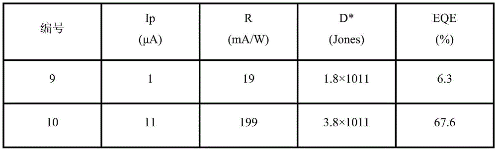
Based on fig. 6(b), (d) and (f), photo-sensitive layer ZnO quantum dots of the same thickness were respectively laid thereon to prepare three photodetectors, numbered 10, 11 and 12. For comparison, a photosensitive layer ZnO quantum dot of the same thickness was laid on a glass substrate and a photodetector was prepared, numbered 9. Wherein the electrode pitch of the photodetector is 200 μm, the electrode length is 4mm, the width is 400 μm, and the height is 90 nm.
As shown in FIG. 8 (a), the alumina pore size was 130 nm. Under different biases, the photocurrents of the photodetectors 10, 11 and 12 all show obvious improvement, and the significant contribution of the light waves captured by the three-dimensional plasma nano-composite structure to the photo-generated carriers is fully proved. In addition, the photodetector 11 obtains the highest photocurrent at each bias, which indicates that when the coverage area of the self-assembled gold nano-antenna is too large, the surface light wave tends to be reflected, thereby causing a certain reduction in the photoelectric effect, as shown by the photodetector 12.
As shown in (b) of fig. 8, at a bias voltage of 10V, each of the photodetectors 10, 11, and 12 exhibits a smooth photoelectric response without significant attenuation over time, indicating that the invention does not affect the stability of the photoresponsive layer.
The main performance parameters of the ZnO photoelectric detector with the three-dimensional plasma nano composite structure are shown in the following table 1, and compared with the photoelectric detector 9 without the three-dimensional plasma nano composite structure, the photoelectric current (Ip) can be maximally increased by 37 times from 1 muA to 37 muA. Accordingly, the responsivity (R) can be increased from 19mA/W to 661 mA/W. The normalized ratio detection rate (D) increased from 1.8 × 10¹¹Jone to 3.3 × 10¹¹ Jone. The External Quantum Efficiency (EQE) is increased from 6.3% to 225.1%, and the effect of the invention on the photoelectric coupling of the photoresponse layer is obvious.
TABLE 1 main performance parameters of ZnO photoelectric detector with three-dimensional plasma nano composite structure

It will be understood by those skilled in the art that the foregoing is only a preferred embodiment of the present invention, and is not intended to limit the invention, and that any modification, equivalent replacement, or improvement made within the spirit and principle of the present invention should be included in the scope of the present invention.
Claims (10)
Priority Applications (1)
| Application Number | Priority Date | Filing Date | Title |
|---|---|---|---|
| CN201910285735.6A CN110190141B (en) | 2019-04-10 | 2019-04-10 | A three-dimensional plasmonic nanocomposite structure and its preparation method and application |
Applications Claiming Priority (1)
| Application Number | Priority Date | Filing Date | Title |
|---|---|---|---|
| CN201910285735.6A CN110190141B (en) | 2019-04-10 | 2019-04-10 | A three-dimensional plasmonic nanocomposite structure and its preparation method and application |
Publications (2)
| Publication Number | Publication Date |
|---|---|
| CN110190141A CN110190141A (en) | 2019-08-30 |
| CN110190141B true CN110190141B (en) | 2021-10-08 |
Family
ID=67714087
Family Applications (1)
| Application Number | Title | Priority Date | Filing Date |
|---|---|---|---|
| CN201910285735.6A Expired - Fee Related CN110190141B (en) | 2019-04-10 | 2019-04-10 | A three-dimensional plasmonic nanocomposite structure and its preparation method and application |
Country Status (1)
| Country | Link |
|---|---|
| CN (1) | CN110190141B (en) |
Family Cites Families (8)
| Publication number | Priority date | Publication date | Assignee | Title |
|---|---|---|---|---|
| KR101244882B1 (en) * | 2012-03-19 | 2013-03-18 | 한국기계연구원 | Anti-reflecting double layer board and manufacturing method thereof |
| US20140175546A1 (en) * | 2012-11-06 | 2014-06-26 | The Regents Of The University Of California | Plasmonically enhanced electro-optic devices and methods of production |
| CN104764732A (en) * | 2015-04-09 | 2015-07-08 | 复旦大学 | Surface-enhanced raman scattering base on basis of special-material superabsorbers and preparation method thereof |
| US10315951B2 (en) * | 2015-06-17 | 2019-06-11 | The Board Of Trustees Of The University Of Illinois | Bowtie nanoantennas and methods of using the same |
| CN107275204B (en) * | 2017-06-20 | 2019-06-28 | 华中科技大学 | A kind of preparation method of nanometer optoelectronic device based on porous anodic alumina template |
| CN107732017B (en) * | 2017-10-10 | 2019-08-13 | 北京大学 | A kind of phasmon structured substrate and its preparation and application |
| CN109256435B (en) * | 2018-09-14 | 2020-07-07 | 闽江学院 | Method for enhancing near-infrared quantum cutting by utilizing silver nano-pillar array structure |
| CN109491002B (en) * | 2018-12-26 | 2020-01-31 | 浙江大学 | porous alumina-based color filter insensitive to incident angle and preparation method thereof |
-
2019
- 2019-04-10 CN CN201910285735.6A patent/CN110190141B/en not_active Expired - Fee Related
Also Published As
| Publication number | Publication date |
|---|---|
| CN110190141A (en) | 2019-08-30 |
Similar Documents
| Publication | Publication Date | Title |
|---|---|---|
| CN108023017B (en) | Single crystal film of organic-inorganic composite perovskite material and preparation method and application thereof | |
| US9490318B2 (en) | Three dimensional strained semiconductors | |
| CN109052470B (en) | A kind of inorganic non-lead cesium bismuth halogen Cs3Bi2X9 perovskite microdisk and its synthesis method | |
| CN114447231A (en) | Preparation method and application of patterned single crystal perovskite array film | |
| CN111525036B (en) | Self-driven perovskite photoelectric detector and preparation method thereof | |
| Zhang et al. | Application of porous silicon microcavity to enhance photoluminescence of ZnO/PS nanocomposites in UV light emission | |
| WO2023165243A1 (en) | Two-dimensional (pea)2pbx4 nanosheet, preparation method therefor, and use thereof in ultraviolet detector | |
| JP2005500702A (en) | Glass bead coating method | |
| Wu et al. | Advances in perovskite single crystal thin films: Synthesis methods and applications in photodetection | |
| CN110416333B (en) | A kind of ultraviolet photodetector and preparation method thereof | |
| CN107217303A (en) | The adjustable CH of diameter3NH3PbI3The synthetic method of perovskite micro wire | |
| CN110190141B (en) | A three-dimensional plasmonic nanocomposite structure and its preparation method and application | |
| Gong et al. | Synthesis and transparent conductivity of crack-free La: BaSnO 3 epitaxial flexible sheets | |
| CN118299445B (en) | Self-powered photoelectric detection device with wide spectral response and preparation method thereof | |
| CN112768610A (en) | Method for uniformly depositing and patterning thin film based on liquid-phase MXene material and large-scale preparation of photoelectric device | |
| US9261627B2 (en) | Zinc oxide anti-reflection layer having a syringe-like structure and method for fabricating the same | |
| US20140213044A1 (en) | Method for producing periodic crystalline silicon nanostructures | |
| CN1438168A (en) | Laser-inducing preparation of size-controllable high-density nano silicon quanta array of points | |
| CN119263196B (en) | Method for making mask plate using deep silicon etching technology and method for preparing halide perovskite array pattern using mask plate | |
| Sontheimer et al. | Light harvesting architectures for electron beam evaporated solid phase crystallized si thin film solar cells: Statistical and periodic approaches | |
| Ranjan et al. | Surface texturization of silicon wafers: A comparative experimental investigation for bulk, industrial application | |
| EP3519161B1 (en) | Process for the production of an organized network of nanowires on a metallic substrate | |
| Liu et al. | Ordered amorphous silicon nanoisland arrays and reflection spectral dependence on nanoisland geometrical parameters | |
| CN120659433B (en) | Crystalline silicon textured surface structure, cells and their fabrication methods, photovoltaic modules | |
| CN103117320B (en) | Based on optical waveguide fluorescence concentration structure and its preparation method of cesium triiodide tin |
Legal Events
| Date | Code | Title | Description |
|---|---|---|---|
| PB01 | Publication | ||
| PB01 | Publication | ||
| SE01 | Entry into force of request for substantive examination | ||
| SE01 | Entry into force of request for substantive examination | ||
| GR01 | Patent grant | ||
| GR01 | Patent grant | ||
| CF01 | Termination of patent right due to non-payment of annual fee | ||
| CF01 | Termination of patent right due to non-payment of annual fee |
Granted publication date: 20211008 |