CN110168891B - Synchronous converter - Google Patents
Synchronous converter Download PDFInfo
- Publication number
- CN110168891B CN110168891B CN201780078897.1A CN201780078897A CN110168891B CN 110168891 B CN110168891 B CN 110168891B CN 201780078897 A CN201780078897 A CN 201780078897A CN 110168891 B CN110168891 B CN 110168891B
- Authority
- CN
- China
- Prior art keywords
- switch
- current
- inductor
- synchronous converter
- control circuit
- Prior art date
- Legal status (The legal status is an assumption and is not a legal conclusion. Google has not performed a legal analysis and makes no representation as to the accuracy of the status listed.)
- Active
Links
Images


Classifications
-
- H—ELECTRICITY
- H02—GENERATION; CONVERSION OR DISTRIBUTION OF ELECTRIC POWER
- H02M—APPARATUS FOR CONVERSION BETWEEN AC AND AC, BETWEEN AC AND DC, OR BETWEEN DC AND DC, AND FOR USE WITH MAINS OR SIMILAR POWER SUPPLY SYSTEMS; CONVERSION OF DC OR AC INPUT POWER INTO SURGE OUTPUT POWER; CONTROL OR REGULATION THEREOF
- H02M3/00—Conversion of DC power input into DC power output
- H02M3/02—Conversion of DC power input into DC power output without intermediate conversion into AC
- H02M3/04—Conversion of DC power input into DC power output without intermediate conversion into AC by static converters
- H02M3/10—Conversion of DC power input into DC power output without intermediate conversion into AC by static converters using discharge tubes with control electrode or semiconductor devices with control electrode
- H02M3/145—Conversion of DC power input into DC power output without intermediate conversion into AC by static converters using discharge tubes with control electrode or semiconductor devices with control electrode using devices of a triode or transistor type requiring continuous application of a control signal
- H02M3/155—Conversion of DC power input into DC power output without intermediate conversion into AC by static converters using discharge tubes with control electrode or semiconductor devices with control electrode using devices of a triode or transistor type requiring continuous application of a control signal using semiconductor devices only
- H02M3/156—Conversion of DC power input into DC power output without intermediate conversion into AC by static converters using discharge tubes with control electrode or semiconductor devices with control electrode using devices of a triode or transistor type requiring continuous application of a control signal using semiconductor devices only with automatic control of output voltage or current, e.g. switching regulators
- H02M3/158—Conversion of DC power input into DC power output without intermediate conversion into AC by static converters using discharge tubes with control electrode or semiconductor devices with control electrode using devices of a triode or transistor type requiring continuous application of a control signal using semiconductor devices only with automatic control of output voltage or current, e.g. switching regulators including plural semiconductor devices as final control devices for a single load
- H02M3/1588—Conversion of DC power input into DC power output without intermediate conversion into AC by static converters using discharge tubes with control electrode or semiconductor devices with control electrode using devices of a triode or transistor type requiring continuous application of a control signal using semiconductor devices only with automatic control of output voltage or current, e.g. switching regulators including plural semiconductor devices as final control devices for a single load comprising at least one synchronous rectifier element
-
- H—ELECTRICITY
- H02—GENERATION; CONVERSION OR DISTRIBUTION OF ELECTRIC POWER
- H02M—APPARATUS FOR CONVERSION BETWEEN AC AND AC, BETWEEN AC AND DC, OR BETWEEN DC AND DC, AND FOR USE WITH MAINS OR SIMILAR POWER SUPPLY SYSTEMS; CONVERSION OF DC OR AC INPUT POWER INTO SURGE OUTPUT POWER; CONTROL OR REGULATION THEREOF
- H02M1/00—Details of apparatus for conversion
- H02M1/08—Circuits specially adapted for the generation of control voltages for semiconductor devices incorporated in static converters
- H02M1/083—Circuits specially adapted for the generation of control voltages for semiconductor devices incorporated in static converters for the ignition at the zero crossing of the voltage or the current
-
- H—ELECTRICITY
- H02—GENERATION; CONVERSION OR DISTRIBUTION OF ELECTRIC POWER
- H02M—APPARATUS FOR CONVERSION BETWEEN AC AND AC, BETWEEN AC AND DC, OR BETWEEN DC AND DC, AND FOR USE WITH MAINS OR SIMILAR POWER SUPPLY SYSTEMS; CONVERSION OF DC OR AC INPUT POWER INTO SURGE OUTPUT POWER; CONTROL OR REGULATION THEREOF
- H02M3/00—Conversion of DC power input into DC power output
- H02M3/02—Conversion of DC power input into DC power output without intermediate conversion into AC
- H02M3/04—Conversion of DC power input into DC power output without intermediate conversion into AC by static converters
- H02M3/10—Conversion of DC power input into DC power output without intermediate conversion into AC by static converters using discharge tubes with control electrode or semiconductor devices with control electrode
- H02M3/145—Conversion of DC power input into DC power output without intermediate conversion into AC by static converters using discharge tubes with control electrode or semiconductor devices with control electrode using devices of a triode or transistor type requiring continuous application of a control signal
- H02M3/155—Conversion of DC power input into DC power output without intermediate conversion into AC by static converters using discharge tubes with control electrode or semiconductor devices with control electrode using devices of a triode or transistor type requiring continuous application of a control signal using semiconductor devices only
- H02M3/156—Conversion of DC power input into DC power output without intermediate conversion into AC by static converters using discharge tubes with control electrode or semiconductor devices with control electrode using devices of a triode or transistor type requiring continuous application of a control signal using semiconductor devices only with automatic control of output voltage or current, e.g. switching regulators
- H02M3/158—Conversion of DC power input into DC power output without intermediate conversion into AC by static converters using discharge tubes with control electrode or semiconductor devices with control electrode using devices of a triode or transistor type requiring continuous application of a control signal using semiconductor devices only with automatic control of output voltage or current, e.g. switching regulators including plural semiconductor devices as final control devices for a single load
-
- H—ELECTRICITY
- H05—ELECTRIC TECHNIQUES NOT OTHERWISE PROVIDED FOR
- H05B—ELECTRIC HEATING; ELECTRIC LIGHT SOURCES NOT OTHERWISE PROVIDED FOR; CIRCUIT ARRANGEMENTS FOR ELECTRIC LIGHT SOURCES, IN GENERAL
- H05B45/00—Circuit arrangements for operating light-emitting diodes [LED]
- H05B45/30—Driver circuits
- H05B45/37—Converter circuits
- H05B45/3725—Switched mode power supply [SMPS]
-
- H—ELECTRICITY
- H02—GENERATION; CONVERSION OR DISTRIBUTION OF ELECTRIC POWER
- H02M—APPARATUS FOR CONVERSION BETWEEN AC AND AC, BETWEEN AC AND DC, OR BETWEEN DC AND DC, AND FOR USE WITH MAINS OR SIMILAR POWER SUPPLY SYSTEMS; CONVERSION OF DC OR AC INPUT POWER INTO SURGE OUTPUT POWER; CONTROL OR REGULATION THEREOF
- H02M1/00—Details of apparatus for conversion
- H02M1/0003—Details of control, feedback or regulation circuits
- H02M1/0009—Devices or circuits for detecting current in a converter
-
- H—ELECTRICITY
- H02—GENERATION; CONVERSION OR DISTRIBUTION OF ELECTRIC POWER
- H02M—APPARATUS FOR CONVERSION BETWEEN AC AND AC, BETWEEN AC AND DC, OR BETWEEN DC AND DC, AND FOR USE WITH MAINS OR SIMILAR POWER SUPPLY SYSTEMS; CONVERSION OF DC OR AC INPUT POWER INTO SURGE OUTPUT POWER; CONTROL OR REGULATION THEREOF
- H02M1/00—Details of apparatus for conversion
- H02M1/0048—Circuits or arrangements for reducing losses
- H02M1/0054—Transistor switching losses
- H02M1/0058—Transistor switching losses by employing soft switching techniques, i.e. commutation of transistors when applied voltage is zero or when current flow is zero
-
- H—ELECTRICITY
- H02—GENERATION; CONVERSION OR DISTRIBUTION OF ELECTRIC POWER
- H02M—APPARATUS FOR CONVERSION BETWEEN AC AND AC, BETWEEN AC AND DC, OR BETWEEN DC AND DC, AND FOR USE WITH MAINS OR SIMILAR POWER SUPPLY SYSTEMS; CONVERSION OF DC OR AC INPUT POWER INTO SURGE OUTPUT POWER; CONTROL OR REGULATION THEREOF
- H02M3/00—Conversion of DC power input into DC power output
- H02M3/02—Conversion of DC power input into DC power output without intermediate conversion into AC
- H02M3/04—Conversion of DC power input into DC power output without intermediate conversion into AC by static converters
- H02M3/10—Conversion of DC power input into DC power output without intermediate conversion into AC by static converters using discharge tubes with control electrode or semiconductor devices with control electrode
- H02M3/145—Conversion of DC power input into DC power output without intermediate conversion into AC by static converters using discharge tubes with control electrode or semiconductor devices with control electrode using devices of a triode or transistor type requiring continuous application of a control signal
- H02M3/155—Conversion of DC power input into DC power output without intermediate conversion into AC by static converters using discharge tubes with control electrode or semiconductor devices with control electrode using devices of a triode or transistor type requiring continuous application of a control signal using semiconductor devices only
- H02M3/156—Conversion of DC power input into DC power output without intermediate conversion into AC by static converters using discharge tubes with control electrode or semiconductor devices with control electrode using devices of a triode or transistor type requiring continuous application of a control signal using semiconductor devices only with automatic control of output voltage or current, e.g. switching regulators
- H02M3/157—Conversion of DC power input into DC power output without intermediate conversion into AC by static converters using discharge tubes with control electrode or semiconductor devices with control electrode using devices of a triode or transistor type requiring continuous application of a control signal using semiconductor devices only with automatic control of output voltage or current, e.g. switching regulators with digital control
-
- H—ELECTRICITY
- H05—ELECTRIC TECHNIQUES NOT OTHERWISE PROVIDED FOR
- H05B—ELECTRIC HEATING; ELECTRIC LIGHT SOURCES NOT OTHERWISE PROVIDED FOR; CIRCUIT ARRANGEMENTS FOR ELECTRIC LIGHT SOURCES, IN GENERAL
- H05B45/00—Circuit arrangements for operating light-emitting diodes [LED]
- H05B45/30—Driver circuits
- H05B45/37—Converter circuits
- H05B45/3725—Switched mode power supply [SMPS]
- H05B45/375—Switched mode power supply [SMPS] using buck topology
-
- H—ELECTRICITY
- H05—ELECTRIC TECHNIQUES NOT OTHERWISE PROVIDED FOR
- H05B—ELECTRIC HEATING; ELECTRIC LIGHT SOURCES NOT OTHERWISE PROVIDED FOR; CIRCUIT ARRANGEMENTS FOR ELECTRIC LIGHT SOURCES, IN GENERAL
- H05B45/00—Circuit arrangements for operating light-emitting diodes [LED]
- H05B45/30—Driver circuits
- H05B45/37—Converter circuits
- H05B45/3725—Switched mode power supply [SMPS]
- H05B45/38—Switched mode power supply [SMPS] using boost topology
-
- Y—GENERAL TAGGING OF NEW TECHNOLOGICAL DEVELOPMENTS; GENERAL TAGGING OF CROSS-SECTIONAL TECHNOLOGIES SPANNING OVER SEVERAL SECTIONS OF THE IPC; TECHNICAL SUBJECTS COVERED BY FORMER USPC CROSS-REFERENCE ART COLLECTIONS [XRACs] AND DIGESTS
- Y02—TECHNOLOGIES OR APPLICATIONS FOR MITIGATION OR ADAPTATION AGAINST CLIMATE CHANGE
- Y02B—CLIMATE CHANGE MITIGATION TECHNOLOGIES RELATED TO BUILDINGS, e.g. HOUSING, HOUSE APPLIANCES OR RELATED END-USER APPLICATIONS
- Y02B70/00—Technologies for an efficient end-user side electric power management and consumption
- Y02B70/10—Technologies improving the efficiency by using switched-mode power supplies [SMPS], i.e. efficient power electronics conversion e.g. power factor correction or reduction of losses in power supplies or efficient standby modes
Landscapes
- Engineering & Computer Science (AREA)
- Power Engineering (AREA)
- Dc-Dc Converters (AREA)
Abstract
A synchronous converter for driving a load (4), comprising: a first switch (M1) coupled in series with a second switch (M2) via a node (x); an inductor (L1) coupled to node (x); input terminals (10, 11) for receiving an input voltage (Vin) from a power supply; output terminals (12, 13) for supplying an output current and an output voltage to a load (4); a first mode in which the first switch (M1) is in an on state and the second switch (M2) is in an off state, and in which the first switch and the inductor (L1) form a series arrangement coupled between the input terminals (10, 11); a second mode in which the first switch (M1) is in an off state and the second switch (M2) is in an on state, and in which the second switch (M2) and the inductor (L1) form a series arrangement coupled between the output terminals (12, 13). The synchronous converter further comprises a control circuit (1), the control circuit (1) comprising: a threshold control circuit (2) for generating a threshold control signal (iq2) for switching off one of the first switch (M1) and the second switch (M2) when a current threshold of a current through the one switch is exceeded, wherein the threshold control circuit has an input for receiving a current signal indicative of the current through the one switch and a comparator for comparing the current signal with the current threshold to obtain the threshold control signal; and an on-time control circuit (3) comprising a calculation unit for directly calculating an on-time of the other of the first switch (M1) and the second switch (M2), wherein the on-time is proportional to the average output current (ILED) and inversely proportional to the output voltage (Vout), and for adjusting the negative peak current (Ineg) to obtain a substantially constant switching frequency of the synchronous converter when the synchronous converter is in the normal operation mode.
Description
Technical Field
The present invention relates to a synchronous converter for providing power to a load. The invention also relates to a method for providing power to a load.
Background
Light Emitting Diodes (LEDs) are used as a type of solid state light source. Its advantages are compactness, high efficiency, good colour, multiple and variable colours, etc. compared with conventional lighting such as incandescent or fluorescent lamps. LEDs are widely used for indoor lighting, decorative lighting, and outdoor lighting. Some of these applications require that the output light of the LED be adjusted to 1% to 100% of the maximum light output.
In the field of drivers, many different topologies of drivers are known. Some of the topologies (e.g., buck converter, boost converter, buck-boost converter) may be configured as synchronous topologies. This results in particular in an efficient driver.
In the field of LED drivers, synchronous converters are well known for driving LED loads. US 2016/0036312 discloses a synchronous buck converter comprising a first switch, a second switch and an inductor. At the beginning of a cycle, the first switch is turned on and the current in the inductor rises. At the end of the rise, the first switch is turned off and the second switch is continuously turned on, and the current in the inductor decays. The second switch may be turned off when the current returns to zero. Then, when a preset value associated with the resonance interval on the switching node exceeds a predefined value, the first switch is turned on again.
US2014/0070780 discloses a control circuit for controlling a switching transistor and a synchronous rectification transistor of a switching regulator, and comprises: a bottom detection comparator configured to assert a make signal; a timer circuit configured to generate a shutdown signal; a zero current detector configured to assert a zero current detection signal; and a drive circuit configured to receive the on signal, the off signal, and the zero-current detection signal, and to (i) turn on the switching transistor and turn off the synchronous rectification transistor when the on signal is asserted, (ii) turn off the switching transistor and turn on the synchronous rectification transistor when the off signal is asserted, and (iii) turn off the switching transistor and the synchronous rectification transistor when the zero-current detection signal is asserted.
US 6151233 discloses a switching power supply circuit in which a synchronous rectification system is employed, when a first switch is switched off, the current IL of the inductive element is maintained by a commutation diode, and the inductive element discharges the energy stored in the conduction period of the first switch. The second switch, which is connected in parallel with the commutation diode, is turned on so as not to overlap with the conduction period of the first switch. In the on period of the second switch, the current IL does not flow through the commutation diode, and the efficiency reduction caused by the forward voltage drop can be prevented. The sense element current detection circuit monitors the current IL and instructs the control circuit to switch off the second switch when the current IL reverses its direction. As a result, no reverse current flows through the inductive element even if the load is small, and thus a switching power supply circuit having high efficiency at all times is realized.
Disclosure of Invention
It is an object of the present invention to provide a synchronous converter and a corresponding conversion method for controlling a buck, boost or buck-boost synchronous converter with increased efficiency. According to a first aspect of the present invention, there is provided a synchronous converter for driving a load, the synchronous converter comprising:
a first switch coupled in series with a second switch via a node;
an inductor coupled to a node;
an input terminal for receiving input power from a power source;
an output terminal for supplying an output current and an output voltage to a load;
wherein the synchronous converter is arranged to operate in a first mode and a second mode,
wherein in the first mode the first switch is in an on-state and the second switch is in an off-state, and the first switch and the inductor form a series arrangement coupled between the input terminals; and
wherein in the second mode the first switch is in an off-state and the second switch is in an on-state, and the second switch and the inductor form a series arrangement coupled between the output terminals;
and wherein the synchronous converter further comprises a control circuit, the control circuit comprising:
a threshold control circuit for generating a threshold control signal for turning off one of the first switch and the second switch when a current threshold of a current through the one switch is exceeded, wherein the threshold control circuit has an input for receiving a current signal indicative of the current through the switch, and a comparator for comparing the current signal with the current threshold; and
on-time control circuit comprising a calculation unit for directly calculating an on-time of the other switch of the first switch and the second switch, wherein the on-time is proportional to the average output current and inversely proportional to the output voltage, and wherein the desired negative peak current (Ineg) is selected such that the switching frequency of the synchronous converter is kept substantially constant.
The synchronous power converter has improved efficiency by using an on-time control circuit to determine the on-time of the other of the first switch and the second switch. The use of an on-time controller allows a more accurate switching moment of the further switch, thereby reducing the peak current. With a lower peak current, the total peak-to-peak current can also be reduced to achieve the same average output current while improving efficiency. A certain negative current peak amplitude may be required to allow the synchronous converter to operate in a zero volt switching mode. If the negative current peak amplitude is too low, zero voltage switching is not possible. If the negative current peak amplitude is too large, additional losses are generated.
In one embodiment, the switching instant of the first switch is controlled by a threshold control circuit which continuously switches off the first switch and switches on the second switch when a threshold control signal is reached. The turn-off instant of the second switch is controlled by the turn-on time control circuit by turning off the second switch after a predetermined or calculated turn-on time of the second switch. The first switch is turned on immediately after or after the turn-off. By means of the on-time control, the negative current peak through the second switch is reduced and, consequently, the positive current peak through the first switch may also be reduced for achieving a desired average output current.
Alternatively, the switching instant of the first switch is controlled by an on-time control circuit, wherein the on-time control circuit successively turns off the first switch and turns on the second switch after the on-time of the first switch. The switching timing of the second switch is controlled by a threshold control circuit that continuously turns off the second switch and turns on the first switch when a threshold control signal is reached. In this way, the peak value of the positive current through the first switch is reduced and, therefore, the peak value of the negative current through the second switch may also be reduced for achieving the desired average output current.
In another embodiment, the synchronous converter comprises a resistor or a transformer for obtaining the current signal through the further switch.
In another embodiment, the on-time controller controls the second switch and the synchronous converter increases the on-time of the second switch when the desired output current should be low. This allows the converter to be synchronized to control the current through the load. If the load comprises an LED, dimming of the LED is obtained by reducing the average output current. During dimming of the load, the increase of the negative current peak amplitude allows a lower average output current without sharp changes of the switching frequency of the first and second switches, since both the positive and negative peak currents can be adjusted for reducing the average output current. Since the synchronous converter can now be operated using a smaller frequency band, the risk of audible noise is reduced.
In another embodiment, the synchronous converter is arranged to operate in only the first mode and the second mode when in the normal operating state.
In another embodiment, the synchronous converter is arranged to operate in a zero voltage switching mode. This improves the efficiency of the synchronous converter even further.
In another embodiment, a system includes a synchronous converter according to the present invention and a load. The load may be an LED load. The LED load may include a single LED or any number of LEDs arranged in any series or parallel arrangement, or any combination thereof.
The synchronous converter may operate in a continuous mode, a discontinuous mode or a critical conduction mode.
According to another embodiment of the invention, there is provided a method for driving a load, the method comprising steps for controlling a buck, boost or buck-boost synchronous power converter, comprising in sequence:
turning on a first switch for storing energy in an inductor;
turning off the first switch when a threshold of the energy stored in the inductor is reached;
switching on the second switch;
calculating an on-period of the second switch, the on-period being proportional to the output current and inversely proportional to the output voltage, an
The second switch is turned off for an on period.
By means of the synchronous converter and the method according to embodiments of the present invention, the LED load can be driven more efficiently.
These embodiments are alternative ways of implementing the switch controlled by the on-time control circuit. These alternatives may include a buck converter, a boost converter, or a buck-boost converter.
Drawings
Examples of the invention will now be described in detail with reference to the accompanying drawings, in which:
figure 1 shows a known synchronous buck converter for driving an LED load,
figure 2 shows a first detailed example of a synchronous buck converter in an embodiment in accordance with the invention,
figure 3 shows a waveform of the inductor current in an embodiment in accordance with the invention,
fig. 4 shows the waveform of the inductor current in an embodiment according to the invention when the output current is reduced,
figure 5 shows two synchronous buck converters in an embodiment in accordance with the invention,
fig. 6 shows a synchronous boost converter in an embodiment in accordance with the invention.
Detailed Description
There are many configurations of switched mode power supplies. The most common configurations are buck converters and boost converters. These converters may be controlled in a synchronous manner. This means that the converter diodes used in buck or boost converters are replaced by switches to reduce conduction losses in the converter. Several configurations of synchronous buck or boost converters will be described in more detail below.
Fig. 1 shows a known synchronous buck converter. The converter comprises input terminals 10, 11 for receiving an input voltage from a power supply and output terminals 12, 13 for supplying an average output current ILED and an output voltage VOUT to the load 4. The converter further comprises a first switch M1, wherein the main current path of the first switch M1 is connected in series with the main current path of the second switch M2 through node x. The not-yet-connected terminal of the main current path of the first switch M1 is also connected to one of the input terminals 10. The not yet connected terminal of the main current path of the second switch M2 is also connected to ground via a sense resistor R2. Inductor L1 is connected to node x on one side and to a pi filter (C-L-C filter) on the other side. The inductor L1 in this example is a transformer, the primary side of which acts as an inductive energy store, and the secondary side acts as a sense winding to sense the amount of current flowing through the primary side. The output of the pi-type filter is connected to one of the output terminals 12. The output terminal 13 which is not connected is connected to ground. The control circuit is connected to the control gates of the first switch M1 and the second switch M2. The controller receives signals from the sense resistor R2 and the secondary winding of the transformer.
The converter is controlled by a control circuit using threshold control of a first switch M1 and a second switch M2. Initially, the first switch M1 is turned on to allow the current through the inductor L1 to increase. When the current through the inductor L1 exceeds a first predetermined threshold, the first switch M1 is turned off. After a predetermined dead time, the second switch M2 is turned on and the current through the inductor begins to decrease. When the inductor current reaches a second predetermined threshold, the second switch M2 is turned off. After a predetermined dead time, the cycle will start over again.
Fig. 2 shows a first example of a synchronous converter for driving a load 4 in an embodiment in accordance with the invention. The synchronous converter may be a synchronous buck converter. The synchronous buck converter comprises input terminals 10, 11 for receiving an input voltage from a power supply, and output terminals 12, 13 for supplying an average output current ILED and an output voltage VOUT to the load 4. The converter further comprises a first switch M1 connected in series with a second switch M2 through node x. The first switch M1 is also connected to the input terminal 10. The second switch M2 is also connected to ground. The converter further comprises an inductor L1, the inductor L1 being connected at one end to node x and at the other end to a pi-filter (C-L-C filter). The inductor L1 in this example is a transformer, with the primary side acting as an inductive energy store and the secondary side acting as a sense winding to sense the amount of current flowing through the primary side. The output of the pi-type filter is connected to one of the output terminals 12. The other output terminal 13 is connected to ground. The control circuit 1 is used to control the first switch M1 and the second switch M2.
In one example, the control of the switches M1, M2 may be performed via a specific control algorithm provided by the control circuit 1. Initially, the first switch M1 is turned on. This allows the current through inductor L1 to increase. When the current exceeds a predefined threshold, the first switch M1 is turned off, and after a predetermined dead time, the second switch M2 is turned on. The current in inductor L1 begins to drop. After a predetermined on-time Ton the second switch M2 is turned off and after a predetermined dead time the cycle will start again.
The switches M1 and M2 are typically implemented as semiconductor bipolar transistors or MOSFETs.
The controller 1 determines a predefined threshold level for the first switch M1 to turn off, and an on-time Ton for the second switch M2 to remain on. To determine the turn-off instant of the first switch M1, the current through the first switch is sensed and converted into a control signal. The control signal is compared with a predefined reference value. When the sensed current exceeds a predefined reference value, the first switch M1 is turned off.
The controller may be an analog circuit that may include a comparator that compares the sensed current with a predefined reference value. The controller may also be a digital controller, such as a Field Programmable Gate Array (FPGA) microprocessor or microcontroller.
The sensed current may be sensed by using a resistor in the path where the current to be measured is required. The voltage drop across the resistor determines the current through the resistor. The current may also be used by using a transformer in the path where the desired measurement current flows. The transformer transforms a current sensed by the primary side into a secondary side signal representing the current flowing through the primary side. Converter inductor L1 may be used as the primary winding of the transformer.
The on-time of the second switch M2 may be selected based on experimental determinations. The on-time may be determined for predetermined L1, Iled, and Vout, for example, such that the desired negative peak current is not too large resulting in additional losses, but not too small resulting in zero-voltage-free switching.
The on-time of the second switch M2 as determined by the controller is preferably determined using the following equation:

in this equation, Ton is the determined on-time of the second switch M2, L1 is the inductance value of inductor L1, Iled is the average output current, Ineg is the desired negative peak current through inductor L1 when zero voltage switching is required, Vout is the output voltage, and Tdelay is the delay caused by the turn-off delay of the second switch M2. In this equation, the parameter Tdelay is a determined optimization of the on-time of the second switch M2. The on-time of the second switch M2 has been improved by using the following equation:

where Iled is the desired average output current determined by taking the average of Ipos (i.e., the desired inductance peak current) and Ineg (the absolute desired negative inductance peak current).
ΔI=Ineg+Ipos
Where Δ I is the peak-to-peak inductor current.

These equations are used to derive the final equation:

fig. 3 shows an example of a current waveform through inductor L1 that may be generated by the circuit shown in fig. 2. The positive peak may be the current peak amplitude determined by a reference threshold provided by the control circuit 1. The negative current peak amplitude may be determined by the determined on-time of the second switch M2.
The determination of the positive and negative current peaks may be reversed. The positive peak may be the peak magnitude of the current determined by the on-time of the first switch M1. The negative current peak may be determined by a determined reference threshold provided by the control circuit 1.
Fig. 4 shows another example of a current waveform flowing through the inductor L1. As can be observed in the figure, the amplitude may vary for positive and negative currents. This may be useful when the converter must be able to drive the load within a certain output voltage range. It is also beneficial to vary the current amplitude when dimming of the load is required.
In one embodiment, the controller 1 receives a dimming signal.
If the dimming signal results in a dimming level above 30% and the output voltage exceeds a predefined output voltage threshold level, the negative current peak amplitude may be set to the minimum amplitude and the positive current peak amplitude is also reduced.
If the dimming signal results in a dimming level above 30% and the output voltage does not exceed the predefined output voltage threshold level, the negative current peak amplitude is increased to guarantee zero voltage switching and the positive current peak amplitude will be decreased for dimming.
If the dimming signal results in a dimming level below 30% and the output voltage exceeds a predefined output voltage threshold level, the negative current peak amplitude is increased for dimming the load and the positive current peak amplitude is decreased.
If the dimming signal results in a dimming level below 30% and the output voltage does not exceed a predefined output voltage threshold level, the negative current peak amplitude is increased for dimming and zero voltage switching of the switch is enabled and the positive current peak amplitude is decreased for dimming.
Depending on the application, the value of the dimming level need not be limited to 30%, but may be selected to have a value suitable for the particular application.
Fig. 5a shows an example of a synchronous buck converter according to the present invention. The converter can operate using the same control algorithm according to the invention. The synchronous buck converter comprises input terminals 10, 11 for receiving an input voltage from a power supply, and output terminals 12, 13 for supplying an output current ILED and an output voltage VOUT to the load LED. The converter further comprises a first switch M1 and a second switch M2, the second switch M2 being connected in series with the first switch M1 via a node x. The first switch M1 is also connected to ground, and the second switch M2 is also connected to the input terminal 10 and the output terminal 12. The converter further comprises an inductor L1, inductor L1 having one end connected to node x and the other end connected to one of the output terminals 12.
Fig. 5b shows another example of a synchronous buck converter according to the present invention. The converter can operate using the same control algorithm according to the invention. The synchronous buck converter comprises input terminals 10, 11 for receiving an input voltage from a power supply, and output terminals 12, 13 for supplying an average output current ILED and an output voltage VOUT to the load 4. The converter further comprises a first switch M1 and a second switch M2, the second switch M2 being connected in series with the first switch M1 via a node x. The first switch M1 is also connected to the input terminal 10, and the second switch M2 is also connected to ground. The converter further comprises an inductor L1, inductor L1 having one end connected to node x and the other end connected to one of the output terminals 12. The other input terminal 11 is interconnected to the output terminal 13 and is connected to the ground level.
FIG. 6 shows one example of a synchronous boost converter using a control algorithm in accordance with the present invention. The synchronous boost converter comprises input terminals 10, 11 for receiving an input voltage from a power supply, and output terminals 12, 13 for supplying an average output current ILED and an output voltage VOUT to the load 4. The converter further comprises a first switch M1 and a second switch M2, the second switch M2 being connected in series with the first switch M1 via a node x. The first switch M1 is also connected to ground 11, and the second switch M2 is also connected to the output terminal 12. The converter further comprises an inductor L1, inductor L1 having one end connected to node x and the other end connected to one of the input terminals 10. The other input terminal 11 is interconnected to the output terminal 13 and is connected to the ground level.
In one example, the control of the switches may be performed via a specific control algorithm provided by the control circuit 1. Initially, the first switch M1 is turned on. This allows current to accumulate in inductor L1. When the current exceeds a predefined threshold, the first switch M1 is turned off, and after a predefined dead time, the second switch M2 is turned on. The current in inductor L1 begins to drop. After a predetermined on-time, the second switch M2 is turned off, and after a predetermined dead time, the cycle will start over.
The on-time of the second switch M2 may be selected based on experimental determinations.
The on-time of the second switch M2 as determined by the controller is preferably determined using the following equation.

In this equation, Ton is the determined on-time of the second switch M2, L1 is the inductance value of inductor L1, Iled is the average output current, Ineg is the desired negative peak current through inductor L1 when zero voltage switching is required, Vout is the output voltage, Vin is the input voltage, and Tdelay is the delay caused by at least the turn-off delay of the second switch M2, but may deviate by the embodiment applied.
In this equation, the parameter Tdelay is a determined optimization of the on-time of the second switch M2. The on-time of the second switch M2 has been improved by:

in the direct calculation of the switch-on duration, it is to be understood that the calculation is carried out before the second mode begins, so that the time period for the switch-on duration during the second mode is calculated. The calculated time period starts at the end of the first mode, immediately before the second mode.
The synchronous converter may be arranged to operate in normal operation only in the first mode and the second mode.
To obtain zero voltage switching of a synchronous converter operating in buck mode, the desired negative peak current can be calculated according to:
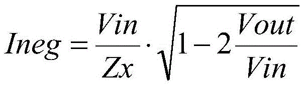
in this equation, Ineg is the desired negative peak current through the inductor (L1), Vin is the input voltage, Vout is the output voltage, and Zx is calculated by:

in this equation, Chb is an equivalent half-bridge capacitance. The capacitance is composed of a plurality of capacitors, which may be the output capacitance and parasitic layout capacitance of the first switch and the second switch.
Other variations to the disclosed embodiments can be understood and effected by those skilled in the art in practicing the claimed invention, from a study of the drawings, the disclosure, and the appended claims. In the claims, the word "comprising" does not exclude other elements or steps, and the indefinite article "a" or "an" does not exclude a plurality. The mere fact that certain measures are recited in mutually different dependent claims does not indicate that a combination of these measures cannot be used to advantage. Any reference signs in the claims shall not be construed as limiting the scope.
Claims (14)
1. A synchronous converter for driving a load (4), the synchronous converter comprising:
a first switch (M1) coupled in series with the second switch (M2) via a node (x);
an inductor (L1) coupled to the node (x);
input terminals (11, 12) for receiving an input voltage from a power supply;
output terminals (13, 14) for supplying an output current and an output voltage to the load (4);
wherein the synchronous converter is arranged to operate in a first mode and a second mode,
wherein in the first mode the first switch (M1) is in an on state and the second switch (M2) is in an off state, and the first switch (M1) and the inductor (L1) form a series arrangement coupled between the input terminals (11, 12); and
wherein in the second mode the first switch (M1) is in an off state and the second switch (M2) is in an on state, and the second switch (M2) and the inductor (L1) form a series arrangement coupled between the output terminals (13, 14);
and wherein the synchronous converter further comprises a control circuit (1), the control circuit (1) comprising:
a threshold control circuit (2) for generating a threshold control signal (Iq2) for switching off one of the first switch (M1) and the second switch (M2) when a current threshold of a current through said one switch is exceeded, wherein the threshold control circuit has an input for receiving a current signal indicative of a current through said one switch (M1, M2), and a comparator for comparing the current signal with the current threshold to obtain the threshold control signal (Iq 2); and
on-time control circuit (3) comprising a calculation unit for directly calculating an on-time of the other one of the first switch (M1) and the second switch (M2), wherein the on-time is proportional to an average output current (Iled) and inversely proportional to an output voltage (Vout), wherein the control circuit (1) is adapted to adjust a negative peak current (Ineg) and a positive peak current (Ipos) to obtain a substantially constant switching frequency of the synchronous converter during dimming of the load (4).
2. The synchronous converter of claim 1, further comprising a resistor or a transformer arranged to obtain a current signal through the one switch.
3. A synchronous converter according to any of the preceding claims, wherein the further switch is the second switch (M2), and wherein the on-time control circuit (3) is arranged for controlling the second switch (M2) and for increasing the on-time of the second switch (M2) to reduce the desired level of the output voltage.
4. A synchronous converter as claimed in any of claims 1-2, wherein the synchronous converter is arranged to operate in normal operation only in the first mode and the second mode.
5. The synchronous converter of claim 4, wherein the converter is configured in a buck configuration, wherein the first switch (M1) and the second switch (M2) are connected in series with the input terminals (11, 12), and the inductor is further connected to one of the output terminals (13, 14).
6. A synchronous converter as claimed in claim 5, wherein the further switch is the second switch, and the on-time control circuit (3) is arranged to calculate the on-time during normal operation as:

wherein Ton is the on-time of the second switch (M2), L1 is an inductance value of the inductor (L1), Iled is the average output current, Ineg is the negative peak current through the inductor (L1), Vout is the output voltage, and Tdelay is a delay caused by the second switch (M2) when turned off.
7. The synchronous converter of claim 4, wherein the converter is arranged in a boost configuration, wherein the first switch (M1) and the second switch (M2) are connected in series with the output terminals (13, 14), and the inductor is further connected to one of the input terminals (11, 12).
8. A synchronous converter as claimed in claim 7, wherein the further switch is the second switch and the on-time control circuit (3) is arranged to calculate the on-time during normal operation as:

wherein Ton is the on-time of the second switch (M2), L1 is an inductance value of the inductor (L1), Iled is the average output current, Ineg is the negative peak current through the inductor (L1), Vout is the output voltage, Vin is the input voltage, and Tdelay is a delay caused by the second switch (M2) when turned off.
9. A synchronous converter according to any of claims 1-2, 5-7 and 8, wherein the control circuit (1) is configured for operating the converter in a zero-voltage switching mode.
10. A synchronous converter according to claim 9 when dependent on claim 5, wherein the desired negative peak current (Ineg) is calculated by:

wherein Ineg is the negative peak current through the inductor (L1), Vin is the input voltage, Vout is the output voltage, and Zx is calculated by:

where L1 is the inductance of the inductor (L1), and Chb is the equivalent half-bridge capacitance.
11. The synchronous converter of claim 1, wherein in an abnormal operating state, the converter is further arranged to operate in a third mode, wherein in the third mode, both the first switch (M1) and the second switch (M2) are in an off state.
12. A system comprising a synchronous converter according to any of the preceding claims, wherein the system further comprises the load (3), and wherein the load (3) is connected to the output terminals (12, 13).
13. The system of claim 12, wherein the load (3) comprises an LED.
14. A method for controlling a synchronous converter according to any of claims 1 to 10, wherein the method comprises the following steps in sequence:
-turning on the first switch (M1) for storing energy in the inductor;
-turn off the first switch (M1) when a threshold value of the energy stored in the inductor is reached;
-turning on the second switch (M2);
-calculating a duration of an on-period of the second switch (M2), said duration being proportional to the average output current (Iled) and inversely proportional to the output voltage (Vout), and
-turning off the second switch at the end of the turn-on period,
wherein the desired negative peak current (Ineg) is selected such that the switching frequency of the synchronous converter remains substantially constant.
Applications Claiming Priority (3)
| Application Number | Priority Date | Filing Date | Title |
|---|---|---|---|
| EP16206154.3 | 2016-12-22 | ||
| EP16206154 | 2016-12-22 | ||
| PCT/EP2017/081510 WO2018114322A1 (en) | 2016-12-22 | 2017-12-05 | Synchronous converter |
Publications (2)
| Publication Number | Publication Date |
|---|---|
| CN110168891A CN110168891A (en) | 2019-08-23 |
| CN110168891B true CN110168891B (en) | 2021-11-19 |
Family
ID=57714429
Family Applications (1)
| Application Number | Title | Priority Date | Filing Date |
|---|---|---|---|
| CN201780078897.1A Active CN110168891B (en) | 2016-12-22 | 2017-12-05 | Synchronous converter |
Country Status (4)
| Country | Link |
|---|---|
| US (1) | US10622894B2 (en) |
| EP (1) | EP3560086B1 (en) |
| CN (1) | CN110168891B (en) |
| WO (1) | WO2018114322A1 (en) |
Families Citing this family (3)
| Publication number | Priority date | Publication date | Assignee | Title |
|---|---|---|---|---|
| EP3871327A1 (en) * | 2018-10-26 | 2021-09-01 | HELLA GmbH & Co. KGaA | Half-bridge with variable dead band control and zero-voltage switching |
| CN110536509B (en) * | 2019-08-09 | 2022-01-07 | 矽力杰半导体技术(杭州)有限公司 | Dimming control method and dimming control circuit and power converter applying same |
| CN114342235B (en) * | 2019-09-30 | 2024-05-28 | 三垦电气株式会社 | Power conversion device |
Citations (7)
| Publication number | Priority date | Publication date | Assignee | Title |
|---|---|---|---|---|
| US6151233A (en) * | 1998-02-10 | 2000-11-21 | Sharp Kabushiki Kaisha | Synchronous rectifier circuit |
| EP1081834A2 (en) * | 1999-08-26 | 2001-03-07 | Texas Instruments Deutschland Gmbh | Methods of operating step-up DC voltage converters and step-up DC voltage converters |
| CN101689805A (en) * | 2007-05-29 | 2010-03-31 | 凌特公司 | Improved Current Mode Control of Switching Regulators |
| CN103078501A (en) * | 2012-12-12 | 2013-05-01 | 青岛联盟电子仪器有限公司 | Dual peak current mode controlled switching power supply converter |
| CN103813587A (en) * | 2014-01-22 | 2014-05-21 | 长安大学 | LED drive circuit with digital-analog hybrid dimming function |
| CN104242644A (en) * | 2014-10-11 | 2014-12-24 | 成都芯源系统有限公司 | Control circuit and control method for switching converter |
| CN105720816A (en) * | 2016-04-14 | 2016-06-29 | 矽力杰半导体技术(杭州)有限公司 | Control circuit and control method of Boost-Buck converter and Boost-Buck converter employing same |
Family Cites Families (16)
| Publication number | Priority date | Publication date | Assignee | Title |
|---|---|---|---|---|
| US6486615B2 (en) * | 1998-10-13 | 2002-11-26 | City University Of Hong Kong | Dimming control of electronic ballasts |
| US8558470B2 (en) * | 2006-01-20 | 2013-10-15 | Point Somee Limited Liability Company | Adaptive current regulation for solid state lighting |
| US20090295300A1 (en) * | 2008-02-08 | 2009-12-03 | Purespectrum, Inc | Methods and apparatus for a dimmable ballast for use with led based light sources |
| US20130176004A1 (en) * | 2012-01-10 | 2013-07-11 | Monolithic Power Systems, Inc. | Switching mode power supply |
| US9559592B2 (en) | 2012-06-18 | 2017-01-31 | Nxp Usa, Inc. | Synchronous rectifier timer for discontinuous mode DC/DC converter |
| JP6106390B2 (en) | 2012-09-13 | 2017-03-29 | ローム株式会社 | Switching regulator, control circuit thereof, control method, and electronic device |
| CN104737626B (en) | 2012-10-18 | 2018-01-26 | 飞利浦照明控股有限公司 | Drive assembly and the driving method for driving load |
| WO2014060872A1 (en) | 2012-10-18 | 2014-04-24 | Koninklijke Philips N.V. | Driver device and driving method for driving a load, in particular an led unit, using a resonant converter |
| US9130457B2 (en) * | 2012-10-24 | 2015-09-08 | Qualcomm Incorporated | Control logic for switches coupled to an inductor |
| KR102016688B1 (en) * | 2012-12-10 | 2019-09-02 | 한국전자통신연구원 | Apparatus for converting energy |
| US9134744B2 (en) * | 2013-01-04 | 2015-09-15 | Linear Technology Corporation | Low current DC-DC converter with integrated low current Coulomb counter |
| US20140312868A1 (en) | 2013-04-23 | 2014-10-23 | Nvidia Corporation | Control of a soft-switched variable frequency multi-phase regulator |
| US10693371B2 (en) | 2014-07-31 | 2020-06-23 | Texas Instruments Incorporated | Method and apparatus for peak switching to reduce losses in high frequency DC-DC converters |
| EP2999107A1 (en) * | 2014-09-18 | 2016-03-23 | Stichting IMEC Nederland | Energy harvesting circuit and method |
| US9525351B2 (en) * | 2014-12-03 | 2016-12-20 | Linear Technology Corporation | Inductor current sensing in a buck converter using multiple filters |
| CN108418427B (en) * | 2018-02-13 | 2020-07-14 | 昂宝电子(上海)有限公司 | System and method for adjusting one or more thresholds in a power converter |
-
2017
- 2017-12-05 EP EP17818466.9A patent/EP3560086B1/en active Active
- 2017-12-05 CN CN201780078897.1A patent/CN110168891B/en active Active
- 2017-12-05 US US16/472,950 patent/US10622894B2/en active Active
- 2017-12-05 WO PCT/EP2017/081510 patent/WO2018114322A1/en unknown
Patent Citations (7)
| Publication number | Priority date | Publication date | Assignee | Title |
|---|---|---|---|---|
| US6151233A (en) * | 1998-02-10 | 2000-11-21 | Sharp Kabushiki Kaisha | Synchronous rectifier circuit |
| EP1081834A2 (en) * | 1999-08-26 | 2001-03-07 | Texas Instruments Deutschland Gmbh | Methods of operating step-up DC voltage converters and step-up DC voltage converters |
| CN101689805A (en) * | 2007-05-29 | 2010-03-31 | 凌特公司 | Improved Current Mode Control of Switching Regulators |
| CN103078501A (en) * | 2012-12-12 | 2013-05-01 | 青岛联盟电子仪器有限公司 | Dual peak current mode controlled switching power supply converter |
| CN103813587A (en) * | 2014-01-22 | 2014-05-21 | 长安大学 | LED drive circuit with digital-analog hybrid dimming function |
| CN104242644A (en) * | 2014-10-11 | 2014-12-24 | 成都芯源系统有限公司 | Control circuit and control method for switching converter |
| CN105720816A (en) * | 2016-04-14 | 2016-06-29 | 矽力杰半导体技术(杭州)有限公司 | Control circuit and control method of Boost-Buck converter and Boost-Buck converter employing same |
Also Published As
| Publication number | Publication date |
|---|---|
| EP3560086A1 (en) | 2019-10-30 |
| EP3560086B1 (en) | 2021-09-15 |
| CN110168891A (en) | 2019-08-23 |
| WO2018114322A1 (en) | 2018-06-28 |
| US20190372461A1 (en) | 2019-12-05 |
| US10622894B2 (en) | 2020-04-14 |
Similar Documents
| Publication | Publication Date | Title |
|---|---|---|
| US11540372B2 (en) | Power converter, LED driver and control method | |
| US9131563B2 (en) | Light-emitting diode driving apparatus and semiconductor device | |
| US8710757B2 (en) | Power converter for an LED assembly and lighting application | |
| EP2536013B1 (en) | A cascade boost and inverting buck converter | |
| US10638562B2 (en) | Power converter, LED driver and control method | |
| JP5693870B2 (en) | Switching power supply circuit | |
| US20130099686A1 (en) | Light emitting diode (led) dimming system | |
| CN107690835B (en) | Operating device, timed flyback converter circuit and method for controlling circuit | |
| EP3365967B1 (en) | Electronic converter and related method of operating an electronic converter | |
| CN110168891B (en) | Synchronous converter | |
| RU2697830C2 (en) | Driver circuit and excitation method | |
| KR101092218B1 (en) | LED Driving Circuit using Sumple Current Source | |
| US8773045B1 (en) | Light emitting diode driving device | |
| KR101942494B1 (en) | Hybrid control type ac direct driving led apparatus | |
| EP3829044B1 (en) | Mixed t_on - t_off modulation for a resonant converter | |
| Sekhar et al. | Input regulated soft switched ripple free current LED driver | |
| JP6245506B2 (en) | Lighting device | |
| JP2017107777A (en) | Lighting device and luminaire having the same | |
| WO2012144274A1 (en) | Led lighting device and led illuminating device | |
| JP2012195251A (en) | Led drive circuit |
Legal Events
| Date | Code | Title | Description |
|---|---|---|---|
| PB01 | Publication | ||
| PB01 | Publication | ||
| SE01 | Entry into force of request for substantive examination | ||
| SE01 | Entry into force of request for substantive examination | ||
| GR01 | Patent grant | ||
| GR01 | Patent grant |