CN109959980B - Hydrophobic mirror and automobile using same - Google Patents
Hydrophobic mirror and automobile using same Download PDFInfo
- Publication number
- CN109959980B CN109959980B CN201711435382.0A CN201711435382A CN109959980B CN 109959980 B CN109959980 B CN 109959980B CN 201711435382 A CN201711435382 A CN 201711435382A CN 109959980 B CN109959980 B CN 109959980B
- Authority
- CN
- China
- Prior art keywords
- hydrophobic
- carbon nanotube
- mirror
- electrode
- layer
- Prior art date
- Legal status (The legal status is an assumption and is not a legal conclusion. Google has not performed a legal analysis and makes no representation as to the accuracy of the status listed.)
- Active
Links
Images


Classifications
-
- B—PERFORMING OPERATIONS; TRANSPORTING
- B32—LAYERED PRODUCTS
- B32B—LAYERED PRODUCTS, i.e. PRODUCTS BUILT-UP OF STRATA OF FLAT OR NON-FLAT, e.g. CELLULAR OR HONEYCOMB, FORM
- B32B17/00—Layered products essentially comprising sheet glass, or glass, slag, or like fibres
- B32B17/06—Layered products essentially comprising sheet glass, or glass, slag, or like fibres comprising glass as the main or only constituent of a layer, next to another layer of a specific material
- B32B17/10—Layered products essentially comprising sheet glass, or glass, slag, or like fibres comprising glass as the main or only constituent of a layer, next to another layer of a specific material of synthetic resin
- B32B17/10005—Layered products essentially comprising sheet glass, or glass, slag, or like fibres comprising glass as the main or only constituent of a layer, next to another layer of a specific material of synthetic resin laminated safety glass or glazing
- B32B17/10009—Layered products essentially comprising sheet glass, or glass, slag, or like fibres comprising glass as the main or only constituent of a layer, next to another layer of a specific material of synthetic resin laminated safety glass or glazing characterized by the number, the constitution or treatment of glass sheets
- B32B17/10018—Layered products essentially comprising sheet glass, or glass, slag, or like fibres comprising glass as the main or only constituent of a layer, next to another layer of a specific material of synthetic resin laminated safety glass or glazing characterized by the number, the constitution or treatment of glass sheets comprising only one glass sheet
-
- B—PERFORMING OPERATIONS; TRANSPORTING
- B32—LAYERED PRODUCTS
- B32B—LAYERED PRODUCTS, i.e. PRODUCTS BUILT-UP OF STRATA OF FLAT OR NON-FLAT, e.g. CELLULAR OR HONEYCOMB, FORM
- B32B17/00—Layered products essentially comprising sheet glass, or glass, slag, or like fibres
- B32B17/06—Layered products essentially comprising sheet glass, or glass, slag, or like fibres comprising glass as the main or only constituent of a layer, next to another layer of a specific material
- B32B17/10—Layered products essentially comprising sheet glass, or glass, slag, or like fibres comprising glass as the main or only constituent of a layer, next to another layer of a specific material of synthetic resin
- B32B17/10005—Layered products essentially comprising sheet glass, or glass, slag, or like fibres comprising glass as the main or only constituent of a layer, next to another layer of a specific material of synthetic resin laminated safety glass or glazing
- B32B17/1055—Layered products essentially comprising sheet glass, or glass, slag, or like fibres comprising glass as the main or only constituent of a layer, next to another layer of a specific material of synthetic resin laminated safety glass or glazing characterized by the resin layer, i.e. interlayer
- B32B17/10614—Layered products essentially comprising sheet glass, or glass, slag, or like fibres comprising glass as the main or only constituent of a layer, next to another layer of a specific material of synthetic resin laminated safety glass or glazing characterized by the resin layer, i.e. interlayer comprising particles for purposes other than dyeing
-
- B—PERFORMING OPERATIONS; TRANSPORTING
- B32—LAYERED PRODUCTS
- B32B—LAYERED PRODUCTS, i.e. PRODUCTS BUILT-UP OF STRATA OF FLAT OR NON-FLAT, e.g. CELLULAR OR HONEYCOMB, FORM
- B32B3/00—Layered products comprising a layer with external or internal discontinuities or unevennesses, or a layer of non-planar shape; Layered products comprising a layer having particular features of form
- B32B3/26—Layered products comprising a layer with external or internal discontinuities or unevennesses, or a layer of non-planar shape; Layered products comprising a layer having particular features of form characterised by a particular shape of the outline of the cross-section of a continuous layer; characterised by a layer with cavities or internal voids ; characterised by an apertured layer
- B32B3/30—Layered products comprising a layer with external or internal discontinuities or unevennesses, or a layer of non-planar shape; Layered products comprising a layer having particular features of form characterised by a particular shape of the outline of the cross-section of a continuous layer; characterised by a layer with cavities or internal voids ; characterised by an apertured layer characterised by a layer formed with recesses or projections, e.g. hollows, grooves, protuberances, ribs
-
- B—PERFORMING OPERATIONS; TRANSPORTING
- B32—LAYERED PRODUCTS
- B32B—LAYERED PRODUCTS, i.e. PRODUCTS BUILT-UP OF STRATA OF FLAT OR NON-FLAT, e.g. CELLULAR OR HONEYCOMB, FORM
- B32B7/00—Layered products characterised by the relation between layers; Layered products characterised by the relative orientation of features between layers, or by the relative values of a measurable parameter between layers, i.e. products comprising layers having different physical, chemical or physicochemical properties; Layered products characterised by the interconnection of layers
- B32B7/04—Interconnection of layers
- B32B7/12—Interconnection of layers using interposed adhesives or interposed materials with bonding properties
-
- B—PERFORMING OPERATIONS; TRANSPORTING
- B60—VEHICLES IN GENERAL
- B60R—VEHICLES, VEHICLE FITTINGS, OR VEHICLE PARTS, NOT OTHERWISE PROVIDED FOR
- B60R1/00—Optical viewing arrangements; Real-time viewing arrangements for drivers or passengers using optical image capturing systems, e.g. cameras or video systems specially adapted for use in or on vehicles
- B60R1/02—Rear-view mirror arrangements
- B60R1/06—Rear-view mirror arrangements mounted on vehicle exterior
- B60R1/0602—Rear-view mirror arrangements mounted on vehicle exterior comprising means for cleaning or deicing
-
- B—PERFORMING OPERATIONS; TRANSPORTING
- B60—VEHICLES IN GENERAL
- B60S—SERVICING, CLEANING, REPAIRING, SUPPORTING, LIFTING, OR MANOEUVRING OF VEHICLES, NOT OTHERWISE PROVIDED FOR
- B60S1/00—Cleaning of vehicles
- B60S1/02—Cleaning windscreens, windows or optical devices
- B60S1/023—Cleaning windscreens, windows or optical devices including defroster or demisting means
- B60S1/026—Cleaning windscreens, windows or optical devices including defroster or demisting means using electrical means
-
- G—PHYSICS
- G02—OPTICS
- G02B—OPTICAL ELEMENTS, SYSTEMS OR APPARATUS
- G02B1/00—Optical elements characterised by the material of which they are made; Optical coatings for optical elements
- G02B1/10—Optical coatings produced by application to, or surface treatment of, optical elements
- G02B1/14—Protective coatings, e.g. hard coatings
-
- G—PHYSICS
- G02—OPTICS
- G02B—OPTICAL ELEMENTS, SYSTEMS OR APPARATUS
- G02B1/00—Optical elements characterised by the material of which they are made; Optical coatings for optical elements
- G02B1/10—Optical coatings produced by application to, or surface treatment of, optical elements
- G02B1/18—Coatings for keeping optical surfaces clean, e.g. hydrophobic or photo-catalytic films
-
- G—PHYSICS
- G02—OPTICS
- G02B—OPTICAL ELEMENTS, SYSTEMS OR APPARATUS
- G02B5/00—Optical elements other than lenses
- G02B5/08—Mirrors
- G02B5/0808—Mirrors having a single reflecting layer
-
- G—PHYSICS
- G02—OPTICS
- G02B—OPTICAL ELEMENTS, SYSTEMS OR APPARATUS
- G02B5/00—Optical elements other than lenses
- G02B5/08—Mirrors
- G02B5/10—Mirrors with curved faces
-
- H—ELECTRICITY
- H05—ELECTRIC TECHNIQUES NOT OTHERWISE PROVIDED FOR
- H05B—ELECTRIC HEATING; ELECTRIC LIGHT SOURCES NOT OTHERWISE PROVIDED FOR; CIRCUIT ARRANGEMENTS FOR ELECTRIC LIGHT SOURCES, IN GENERAL
- H05B3/00—Ohmic-resistance heating
- H05B3/10—Heating elements characterised by the composition or nature of the materials or by the arrangement of the conductor
- H05B3/12—Heating elements characterised by the composition or nature of the materials or by the arrangement of the conductor characterised by the composition or nature of the conductive material
- H05B3/14—Heating elements characterised by the composition or nature of the materials or by the arrangement of the conductor characterised by the composition or nature of the conductive material the material being non-metallic
- H05B3/141—Conductive ceramics, e.g. metal oxides, metal carbides, barium titanate, ferrites, zirconia, vitrous compounds
-
- H—ELECTRICITY
- H05—ELECTRIC TECHNIQUES NOT OTHERWISE PROVIDED FOR
- H05B—ELECTRIC HEATING; ELECTRIC LIGHT SOURCES NOT OTHERWISE PROVIDED FOR; CIRCUIT ARRANGEMENTS FOR ELECTRIC LIGHT SOURCES, IN GENERAL
- H05B3/00—Ohmic-resistance heating
- H05B3/10—Heating elements characterised by the composition or nature of the materials or by the arrangement of the conductor
- H05B3/12—Heating elements characterised by the composition or nature of the materials or by the arrangement of the conductor characterised by the composition or nature of the conductive material
- H05B3/14—Heating elements characterised by the composition or nature of the materials or by the arrangement of the conductor characterised by the composition or nature of the conductive material the material being non-metallic
- H05B3/145—Carbon only, e.g. carbon black, graphite
-
- H—ELECTRICITY
- H05—ELECTRIC TECHNIQUES NOT OTHERWISE PROVIDED FOR
- H05B—ELECTRIC HEATING; ELECTRIC LIGHT SOURCES NOT OTHERWISE PROVIDED FOR; CIRCUIT ARRANGEMENTS FOR ELECTRIC LIGHT SOURCES, IN GENERAL
- H05B3/00—Ohmic-resistance heating
- H05B3/20—Heating elements having extended surface area substantially in a two-dimensional plane, e.g. plate-heater
- H05B3/34—Heating elements having extended surface area substantially in a two-dimensional plane, e.g. plate-heater flexible, e.g. heating nets or webs
-
- H—ELECTRICITY
- H05—ELECTRIC TECHNIQUES NOT OTHERWISE PROVIDED FOR
- H05B—ELECTRIC HEATING; ELECTRIC LIGHT SOURCES NOT OTHERWISE PROVIDED FOR; CIRCUIT ARRANGEMENTS FOR ELECTRIC LIGHT SOURCES, IN GENERAL
- H05B3/00—Ohmic-resistance heating
- H05B3/84—Heating arrangements specially adapted for transparent or reflecting areas, e.g. for demisting or de-icing windows, mirrors or vehicle windshields
- H05B3/845—Heating arrangements specially adapted for transparent or reflecting areas, e.g. for demisting or de-icing windows, mirrors or vehicle windshields specially adapted for reflecting surfaces, e.g. bathroom - or rearview mirrors
-
- B—PERFORMING OPERATIONS; TRANSPORTING
- B32—LAYERED PRODUCTS
- B32B—LAYERED PRODUCTS, i.e. PRODUCTS BUILT-UP OF STRATA OF FLAT OR NON-FLAT, e.g. CELLULAR OR HONEYCOMB, FORM
- B32B2264/00—Composition or properties of particles which form a particulate layer or are present as additives
- B32B2264/10—Inorganic particles
-
- B—PERFORMING OPERATIONS; TRANSPORTING
- B32—LAYERED PRODUCTS
- B32B—LAYERED PRODUCTS, i.e. PRODUCTS BUILT-UP OF STRATA OF FLAT OR NON-FLAT, e.g. CELLULAR OR HONEYCOMB, FORM
- B32B2307/00—Properties of the layers or laminate
- B32B2307/40—Properties of the layers or laminate having particular optical properties
- B32B2307/416—Reflective
-
- B—PERFORMING OPERATIONS; TRANSPORTING
- B32—LAYERED PRODUCTS
- B32B—LAYERED PRODUCTS, i.e. PRODUCTS BUILT-UP OF STRATA OF FLAT OR NON-FLAT, e.g. CELLULAR OR HONEYCOMB, FORM
- B32B2307/00—Properties of the layers or laminate
- B32B2307/70—Other properties
- B32B2307/73—Hydrophobic
-
- G—PHYSICS
- G02—OPTICS
- G02B—OPTICAL ELEMENTS, SYSTEMS OR APPARATUS
- G02B2207/00—Coding scheme for general features or characteristics of optical elements and systems of subclass G02B, but not including elements and systems which would be classified in G02B6/00 and subgroups
- G02B2207/101—Nanooptics
-
- H—ELECTRICITY
- H05—ELECTRIC TECHNIQUES NOT OTHERWISE PROVIDED FOR
- H05B—ELECTRIC HEATING; ELECTRIC LIGHT SOURCES NOT OTHERWISE PROVIDED FOR; CIRCUIT ARRANGEMENTS FOR ELECTRIC LIGHT SOURCES, IN GENERAL
- H05B2203/00—Aspects relating to Ohmic resistive heating covered by group H05B3/00
- H05B2203/013—Heaters using resistive films or coatings
-
- H—ELECTRICITY
- H05—ELECTRIC TECHNIQUES NOT OTHERWISE PROVIDED FOR
- H05B—ELECTRIC HEATING; ELECTRIC LIGHT SOURCES NOT OTHERWISE PROVIDED FOR; CIRCUIT ARRANGEMENTS FOR ELECTRIC LIGHT SOURCES, IN GENERAL
- H05B2214/00—Aspects relating to resistive heating, induction heating and heating using microwaves, covered by groups H05B3/00, H05B6/00
- H05B2214/03—Heating of hydrocarbons
-
- H—ELECTRICITY
- H05—ELECTRIC TECHNIQUES NOT OTHERWISE PROVIDED FOR
- H05B—ELECTRIC HEATING; ELECTRIC LIGHT SOURCES NOT OTHERWISE PROVIDED FOR; CIRCUIT ARRANGEMENTS FOR ELECTRIC LIGHT SOURCES, IN GENERAL
- H05B2214/00—Aspects relating to resistive heating, induction heating and heating using microwaves, covered by groups H05B3/00, H05B6/00
- H05B2214/04—Heating means manufactured by using nanotechnology
Landscapes
- Physics & Mathematics (AREA)
- Engineering & Computer Science (AREA)
- General Physics & Mathematics (AREA)
- Optics & Photonics (AREA)
- Mechanical Engineering (AREA)
- Multimedia (AREA)
- Chemical & Material Sciences (AREA)
- Chemical Kinetics & Catalysis (AREA)
- Ceramic Engineering (AREA)
- Laminated Bodies (AREA)
- Carbon And Carbon Compounds (AREA)
Abstract
本发明提供一种疏水镜子,其包括一支撑体、一设置于该支撑体上的镜子本体和一疏水膜,所述疏水膜设置于所述镜子本体的表面,所述疏水膜包括一柔性衬底,该柔性衬底包括一柔性基底以及设置于该柔性基底表面上的图案化的第一凸起;以及一疏水层,所述疏水层设置于该柔性衬底具有图案化的第一凸起的表面。
The present invention provides a hydrophobic mirror, which includes a support body, a mirror body disposed on the support body, and a hydrophobic film, the hydrophobic film is disposed on the surface of the mirror body, and the hydrophobic film includes a flexible lining bottom, the flexible substrate includes a flexible base and patterned first protrusions disposed on the surface of the flexible base; and a hydrophobic layer, the hydrophobic layer is disposed on the flexible substrate and has patterned first protrusions s surface.
Description
技术领域technical field
本发明涉及一种疏水膜,尤其涉及一种疏水镜子以及使用该疏水镜子的汽车。The present invention relates to a hydrophobic film, in particular to a hydrophobic mirror and an automobile using the hydrophobic mirror.
背景技术Background technique
疏水结构在现实生活中有重要的应用,如窗户、镜子等。现有的疏水镜子是在镜子本体上直接刻蚀形成疏水槽达到疏水的目的。当所述疏水镜子的疏水性能减弱时或所述疏水槽损坏时,往往需要更换整个疏水镜子,但是更换整个疏水镜子比较费时费力以及增加成本。Hydrophobic structures have important applications in real life, such as windows, mirrors, etc. In the existing hydrophobic mirror, a hydrophobic groove is formed by directly etching the mirror body to achieve the purpose of hydrophobicity. When the hydrophobic performance of the hydrophobic mirror is weakened or the hydrophobic groove is damaged, the entire hydrophobic mirror often needs to be replaced, but the replacement of the entire hydrophobic mirror is time-consuming, labor-intensive and cost-increasing.
发明内容SUMMARY OF THE INVENTION
有鉴于此,确有必要提供一种能够更换疏水膜的的疏水镜子。In view of this, it is indeed necessary to provide a hydrophobic mirror that can replace the hydrophobic membrane.
一种疏水镜子,其包括一支撑体、一设置于该支撑体上的镜子本体和一疏水膜,所述疏水膜设置于所述镜子本体的表面,所述疏水膜包括一柔性衬底,该柔性衬底包括一柔性基底以及设置于该柔性基底表面上的图案化的第一凸起;以及一疏水层,所述疏水层设置于该柔性衬底具有图案化的第一凸起的表面。A hydrophobic mirror, comprising a support body, a mirror body disposed on the support body, and a hydrophobic film, the hydrophobic film being disposed on the surface of the mirror body, the hydrophobic film comprising a flexible substrate, the The flexible substrate includes a flexible substrate and patterned first protrusions disposed on the surface of the flexible substrate; and a hydrophobic layer disposed on the surface of the flexible substrate with the patterned first protrusions.
一种汽车,所述汽车包括一车体以及设置于该车体上的镜子,其中,所述镜子为上述具备疏水功能的疏水镜子。An automobile, comprising a body and a mirror arranged on the body, wherein the mirror is the above-mentioned hydrophobic mirror with a hydrophobic function.
与现有技术相比,本发明所提供的疏水镜子具有以下优点,第一,采用柔性衬底制备得到的疏水膜具有一定的柔韧性,可设置在曲面上并与曲面贴合。第二,所制备的疏水层表面的纳米结构的图案化的第一凸起可以提高疏水膜的疏水性能。第三,所述柔性衬底远离疏水层的表面设置一粘结剂层和一保护层,便于储存和使用。第四,所述疏水镜子还可以进行通电加热实现加热除冰/霜/雾 /雨。Compared with the prior art, the hydrophobic mirror provided by the present invention has the following advantages. First, the hydrophobic film prepared by using a flexible substrate has certain flexibility, and can be arranged on and attached to a curved surface. Second, the patterned first protrusions of the nanostructure on the surface of the prepared hydrophobic layer can improve the hydrophobic performance of the hydrophobic film. Third, an adhesive layer and a protective layer are provided on the surface of the flexible substrate away from the hydrophobic layer, which is convenient for storage and use. Fourth, the hydrophobic mirror can also be electrically heated to achieve heating and deicing/frost/fog/rain.
附图说明Description of drawings
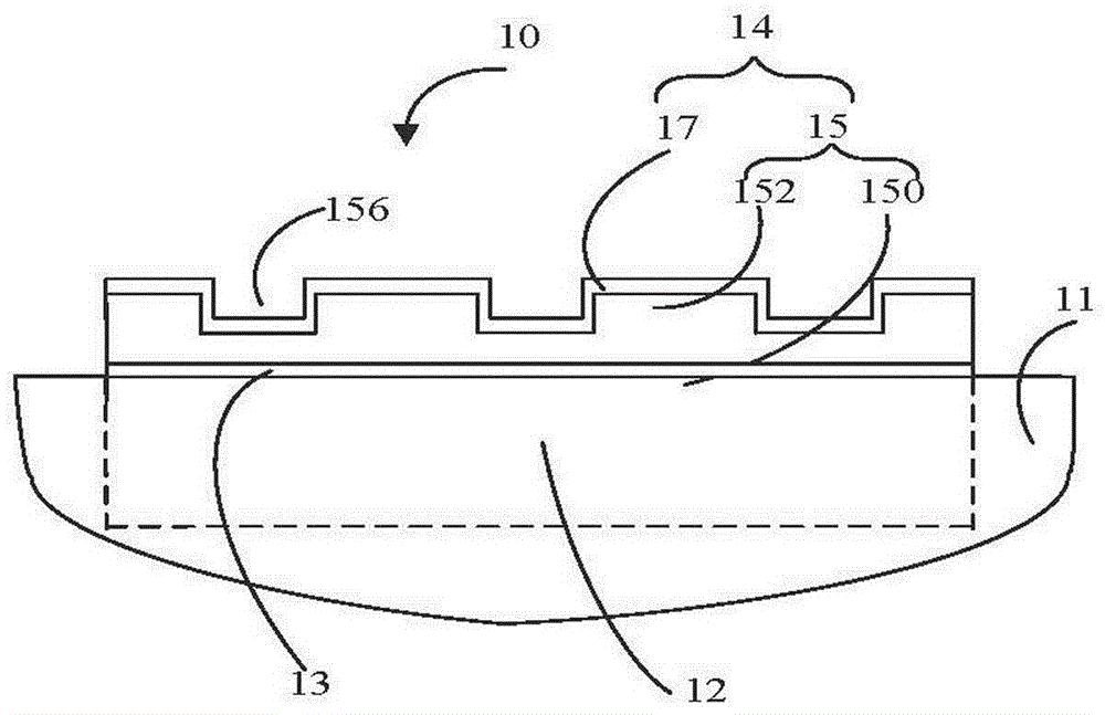
图1为本发明第一实施例提供的疏水镜子的结构示意图。FIG. 1 is a schematic structural diagram of a hydrophobic mirror provided by a first embodiment of the present invention.
图2为本发明第一实施例提供的疏水膜的立体结构示意图。FIG. 2 is a schematic three-dimensional structure diagram of the hydrophobic membrane provided by the first embodiment of the present invention.
图3为本图2所提供的疏水膜沿III-III方向的剖视图。FIG. 3 is a cross-sectional view of the hydrophobic membrane provided in FIG. 2 along the III-III direction.
图4为本发明第一实施例提供的另一疏水膜的结构示意图。FIG. 4 is a schematic structural diagram of another hydrophobic membrane provided by the first embodiment of the present invention.
图5为本发明第一实施例提供的疏水膜的制备方法流程图。FIG. 5 is a flow chart of the preparation method of the hydrophobic membrane provided by the first embodiment of the present invention.
图6为本发明第一实施例提供的模板的制备方法流程图。FIG. 6 is a flowchart of a method for preparing a template provided by the first embodiment of the present invention.
图7为图6的碳纳米管复合结构的沿线VII-VII的截面图。FIG. 7 is a cross-sectional view along line VII-VII of the carbon nanotube composite structure of FIG. 6 .
图8为本发明第一实施例采用的碳纳米管拉膜的扫描电镜照片。FIG. 8 is a scanning electron microscope photograph of the carbon nanotube-drawn film used in the first embodiment of the present invention.
图9为本发明第一实施例采用的非扭转的碳纳米管线的扫描电镜照片。FIG. 9 is a scanning electron microscope photograph of the non-twisted carbon nanotube wire used in the first embodiment of the present invention.
图10为本发明第一实施例采用的扭转的碳纳米管线的扫描电镜照片。FIG. 10 is a scanning electron microscope photograph of the twisted carbon nanotubes used in the first embodiment of the present invention.
图11为本发明第一实施例提供的碳纳米管复合结构的扫描电镜照片。FIG. 11 is a scanning electron microscope photograph of the carbon nanotube composite structure provided in the first embodiment of the present invention.
图12为本发明第一实施例提供的碳纳米管复合结构的包覆三氧化二铝层的单根碳纳米管的扫描电镜照片。12 is a scanning electron microscope photograph of a single carbon nanotube coated with an aluminum oxide layer of the carbon nanotube composite structure provided in the first embodiment of the present invention.
图13为本发明第一实施例提供的疏水膜的扫描电镜照片。FIG. 13 is a scanning electron microscope photograph of the hydrophobic film provided by the first embodiment of the present invention.
图14为本发明第一实施例提供的疏水膜的性能测试图。FIG. 14 is a performance test diagram of the hydrophobic membrane provided by the first embodiment of the present invention.
图15为本发明第二实施例提供的疏水镜子的结构示意图。FIG. 15 is a schematic structural diagram of a hydrophobic mirror provided by a second embodiment of the present invention.
图16为本发明第二实施例提供的疏水膜的制备方法。FIG. 16 is the preparation method of the hydrophobic membrane provided by the second embodiment of the present invention.
图17为本发明第三实施例提供的疏水镜子的结构示意图。FIG. 17 is a schematic structural diagram of a hydrophobic mirror provided by a third embodiment of the present invention.
图18为本发明第四实施例提供的疏水镜子的结构示意图。FIG. 18 is a schematic structural diagram of a hydrophobic mirror provided by a fourth embodiment of the present invention.
图19为本发明第四实施例提供的疏水膜的制备方法流程图。FIG. 19 is a flow chart of the preparation method of the hydrophobic membrane provided by the fourth embodiment of the present invention.
图20为本发明第五实施例提供的疏水镜子的结构示意图。FIG. 20 is a schematic structural diagram of a hydrophobic mirror provided by a fifth embodiment of the present invention.
图21为本发明第六实施例提供的疏水镜子的结构示意图。FIG. 21 is a schematic structural diagram of a hydrophobic mirror provided by a sixth embodiment of the present invention.
图22为本发明第七实施例提供的疏水镜子的结构示意图。FIG. 22 is a schematic structural diagram of a hydrophobic mirror provided by a seventh embodiment of the present invention.
图23为本发明第八实施例提供的使用本发明第一实施例提供的疏水镜子的汽车的结构示意图。23 is a schematic structural diagram of an automobile using the hydrophobic mirror provided by the first embodiment of the present invention according to the eighth embodiment of the present invention.
主要元件符号说明Description of main component symbols


具体实施方式Detailed ways
如下具体实施方式将结合上述附图进一步说明本发明。The following specific embodiments will further illustrate the present invention in conjunction with the above drawings.
参见图1,本发明提供一种疏水镜子10,其包括一支撑体11、一设置于该支撑体11上的镜子本体12和一疏水膜14,所述疏水膜14设置于所述镜子本体 12的表面,该疏水膜14包括一柔性衬底15和一疏水层17。所述柔性衬底15 包括一柔性基底150以及设置于该柔性基底150表面上的图案化的第一凸起 152;所述图案化的第一凸起152与所述柔性基底150为一体结构;所述图案化的第一凸起152包括多个凸块,所述多个凸块间隔设置呈二维阵列,从而定义多个第一凹槽156,所述疏水层17设置于该柔性衬底15具有图案化的第一凸起152的表面。Referring to FIG. 1 , the present invention provides a
参见图2(A)和图3(A),所述图案化的第一凸起152包括多个凸块,所述多个凸块间隔设置呈二维阵列,从而定义多个第一凹槽156。参见图2(B) 和图3(B),所述图案化的第一凸起152包括多个凸条,所述多个凸条交叉设置形成网状结构,所述多个凸条的交叉处为一体结构,从而定义多个第一孔洞157。本实施例以图2(A)和图3(A)为例进行说明。Referring to FIGS. 2(A) and 3(A) , the patterned
所述镜子本体12包括一镜面和与镜面相对的表面,所述镜面120是指能够看到镜像的表面,与镜面相对的表面是指镀有银的表面,所述疏水膜14设置于所述镜子本体12的镜面上。The
所述疏水膜14可以通过粘结剂层13设置于需要疏水的物体的表面。因此所述疏水膜14可以随时更换,当所述疏水膜14受到损坏时,可以仅更换疏水膜14而不需要更换整个物体,进而可以节约成本。请一并参见图4,所述疏水膜14也可以进一步包括一粘结剂层13和一保护层130,这样在使用时可以直接除去保护层130,然后将疏水膜14直接设置于需要疏水的物体的表面,避免临时在需要疏水的物体的表面设置粘结剂层13,便于储存和使用。The
所述柔性衬底15为一柔性透明薄膜,该柔性衬底15可以赋予所述疏水膜 14一定的柔韧性,进而可以将所述疏水膜14贴合于曲面上。具体地,该柔性衬底15的材料可以为聚对苯二甲酸乙二醇酯(PET)、聚酰亚胺(PI)、聚甲基丙烯酸甲酯(PMMA)、聚二甲基硅氧烷(PDMS)、聚萘二甲酸乙二醇酯(PEN)等。本实施例中,所述柔性衬底15的材料为聚对苯二甲酸乙二醇酯。所述柔性衬底15的形状、大小及厚度不限,可根据需要选择。本实施例中,所述柔性衬底15的形状为一矩形,厚度为800纳米-800微米,更优选地,所述厚度为60微米-300微米。The
所述柔性基底150与所述图案化的第一凸起152的多个凸块是材料相同的一体结构。所述图案化的第一凸起152设置于所述柔性基底150的一个表面。每个凸块的宽度为15纳米-800纳米,优选地,每个凸块的宽度为30纳米-400 纳米,更优选地,每个凸块的宽度为60纳米-200纳米;高度为75纳米-800纳米,优选地,所述高度为80纳米-450纳米,平行且相邻的凸块之间的间距为25 纳米-600纳米,优选地,30纳米-135纳米。因此,所述第一凹槽156的开口尺寸为25纳米-600纳米,深度为80纳米-400纳米。本实施例中,所述凸块的宽度为40纳米-80纳米,高度为120纳米-300纳米,平行且相邻的凸块之间的间距为30纳米-80纳米。所述图2(A)所示的图案化的第一凸起152与图2(B) 所示的图案化的第一凸起152的结构互补。The
所述疏水层17设置于所述柔性衬底15具有图案化的第一凸起152的表面。所述疏水层17可以为连续的层状结构,也可以为非连续的层状结构。具体地,所述疏水层17设置于所述多个凸块表面以及凸块之间的第一凹槽156内。所述疏水层17可以为单层层状结构或多层层状结构。所述疏水层17基本均匀沉积于凸块表面以及凸块之间的第一凹槽156内。所述疏水层17的厚度为10纳米-180纳米,优选地,所述疏水层17的厚度为35纳米-150纳米。更优选地,所述疏水层17的厚度为60纳米-80纳米。本实施例中,所述疏水层17的厚度为 70纳米。所述疏水层17的材料可为二氧化硅、氮化硅等绝缘材料,或氮化镓、砷化镓等半导体材料。本实施例中,所述疏水层的材料为二氧化硅。The
参见图5,本发明第一实施例提供一种制备上述疏水膜14的制备方法:Referring to FIG. 5, the first embodiment of the present invention provides a preparation method for preparing the above-mentioned hydrophobic film 14:
S11,提供一硬质基底21;S11, providing a
S12,在所述硬质基底21的表面设置一高分子层22,对所述高分子层22 进行烘烤,使所述高分子层22成半固体状态;S12, disposing a
S13,提供一模板23,将所述模板23具有纳米图形的一侧与所述高分子层 22贴合,将模板23上的纳米图形转移到所述高分子层22的表面;S13, providing a
S14,去除所述模板23得到柔性衬底15;S14, removing the
S15,在所述柔性衬底15具有纳米图形的表面设置一疏水层17。S15, a
在步骤S11中,所述硬质基底21对所述高分子层22起支撑作用。所述硬质基底21的尺寸和厚度可以根据需要选择。本实施例中,所述硬质基底21为一厚度为0.5mm-1.2mm的二氧化硅。In step S11 , the
在步骤S12中,所述高分子层22应具有可在室温下压印、结构稳定性好以及压印分辨率可达到10纳米以下的高分辨率等特性,具体地,所述高分子层22 的材料为PMMA、PI、PDMS等。本实施例中,所述高分子层22的材料为PMMA。In step S12, the
可以通过旋涂或液滴涂布的方式设置高分子层22。本实施例中所述高分子层22的制备方法包括以下步骤:首先,提供一PMMA溶液;在所述硬质基底 21的表面旋涂PMMA,旋涂转速为500转/分钟-6000转/分钟,时间为0.5分钟-1.5分钟。其次,低温烘烤所述PMMA,使所述PMMA成半固体状态。本发明第一实施例中,在低温烘烤3分钟-5分钟,从而在所述硬质基底21的表面形成一完整的高分子层22。所述低温为在50℃以下的温度。该高分子层22的厚度为600纳米-8毫米。优选地,所述高分子层22的厚度为1毫米-4毫米。更优选地,所述高分子层22的厚度为60微米-800微米。更优选地,所述高分子层 22的厚度为100微米-300微米。本实施例中,所述高分子层22的厚度为200 微米。The
在步骤S13中,所述模板23包括图案化的第三凸起232。所述图案化的第三凸起232包括多个凸条交叉设置形成网状结构,从而定义多个第三孔洞234。所述模板23的材料为硬性材料,如镍、硅、二氧化硅等。本发明实施例中所述模板23的材料为二氧化硅。In step S13 , the
请一并参见图6和图7,本发明第一实施例提供的制备所述模板23的方法,包括以下步骤:Please refer to FIG. 6 and FIG. 7 together, the method for preparing the
S131,提供一基体230;S131, providing a
S132,提供一具有多个微孔116的碳纳米管结构110,该碳纳米管结构110 包括多个交叉设置的碳纳米管;S132, providing a
S133,将所述碳纳米管结构110设置于所述基体230的一表面236,从而使所述基体230的表面236部分暴露;S133, disposing the
S134,以该碳纳米管结构110为掩模干法刻蚀所述基体230,从而得到一具有图案化的第三凸起232的模板23,且该图案化的第三凸起232包括多个交叉设置的凸条;S134 , dry etching the
S135,去除所述碳纳米管结构110。S135, removing the
在步骤S131中,所述基体230的材料不限,可为二氧化硅、氮化硅等材料,也可以为金、铝、镍、铬、铜等金属材料或者硅、氮化镓、砷化镓等半导体材料,只要所述基体230在后续的刻蚀过程中,可被刻蚀即可。In step S131, the material of the
在步骤S132中,所述碳纳米管结构110包括多个有序排列的碳纳米管,从而形成多个开口,该多个开口从所述碳纳米管结构110的厚度方向贯穿所述碳纳米管结构110。所述开口可以为微孔或间隙。所述尺寸是指所述微孔的孔径或所述间隙的宽度方向的间距。所述开口的尺寸为2纳米-500微米、或20纳米-60 微米、或80纳米-5微米、或200纳米-1.5微米。所述碳纳米管结构110可以为纯碳纳米管结构111或碳纳米管复合结构112。所述纯碳纳米管结构111指碳纳米管结构110中仅包括多个碳纳米管,不包括其它成分。所述碳纳米管复合结构112包括一纯碳纳米管结构111以及一包覆于该纯碳纳米管结构111表面的预制层114。所述预制层114包覆于该多个碳纳米管的表面。优选地,所述预制层 114包覆于每个碳纳米管的整个表面。所述碳纳米管包括单壁碳纳米管、双壁碳纳米管及多壁碳纳米管中的一种或多种。所述碳纳米管平行于所述纯碳纳米管结构111的表面。所述单壁碳纳米管的直径为0.5纳米-10纳米,双壁碳纳米管的直径为1.0纳米-15纳米,多壁碳纳米管的直径为1.5纳米-500纳米。所述碳纳米管的长度大于50微米。优选地,该碳纳米管的长度为200微米-900微米。In step S132 , the
所述纯碳纳米管结构111包括多个有序排列且交叉设置的碳纳米管从而形成多个微孔,所述预制层114包覆于该多个碳纳米管的表面。优选地,所述预制层114包覆于每个碳纳米管的整个表面。所述多个碳纳米管通过范德华力紧密连接从而使该纯碳纳米管结构111及碳纳米管复合结构112形成一自支撑结构。所谓自支撑结构是指该结构可以无需一支撑体而保持一特定的膜状结构。因而,所述碳纳米管复合结构112具有自支撑性而可部分悬空设置。The pure
所述纯碳纳米管结构111包括至少一碳纳米管膜、至少一碳纳米管线或其组合。所述碳纳米管膜包括多个均匀分布的碳纳米管。该碳纳米管膜中的多个碳纳米管沿一个方向延伸,该多个碳纳米管组成多个碳纳米管束,所述碳纳米管的延伸方向平行于所述碳纳米管膜的表面。具体地,该碳纳米管膜可包括一碳纳米管拉膜。该碳纳米管线可以为一非扭转的碳纳米管线或扭转的碳纳米管线。当所述纯碳纳米管结构111包括多个碳纳米管线时,该多个碳纳米管线相互平行间隔且呈一定角度交叉排列而形成一层状的碳纳米管结构。该层状的碳纳米管结构包括多个微孔,该微孔为一贯穿该层状的碳纳米管结构的厚度方向的通孔。该微孔的尺寸为1纳米-0.5微米。The pure
请参阅图8,具体地,该碳纳米管拉膜包括多个连续且定向排列的碳纳米管束。该多个碳纳米管束通过范德华力首尾相连。每一碳纳米管束包括多个相互平行的碳纳米管,该多个相互平行的碳纳米管通过范德华力紧密结合。该碳纳米管束的直径为10纳米-200纳米,优选的,10纳米-100纳米。该碳纳米管拉膜中的碳纳米管沿同一方向择优取向排列。所述碳纳米管拉膜包括多个微孔。该微孔为一贯穿该层状的碳纳米管结构的厚度方向的通孔。该微孔可为孔隙和/或间隙。当所述纯碳纳米管结构111仅包括单层碳纳米管拉膜时,该碳纳米管拉膜中相邻的碳纳米管片段之间具有间隙,其中,该间隙的尺寸为1纳米-0.5微米。可以理解,在由多层碳纳米管拉膜组成的纯碳纳米管结构111中,相邻两个碳纳米管拉膜中的碳纳米管的排列方向有一夹角α,且0°<α≤90°,从而使相邻两层碳纳米管拉膜中的碳纳米管相互交叉组成一网状结构,该网状结构包括多个孔隙,该多个孔隙均匀且规则分布于纯碳纳米管结构111中,其中,该孔隙直径为1纳米-0.5微米。所述碳纳米管拉膜的厚度为0.01微米-100微米。所述碳纳米管拉膜可以通过拉取一碳纳米管阵列直接获得。所述碳纳米管拉膜的结构及其制备方法请参见范守善等人于2007年2月9日申请的,于2010年5 月26日公告的第CN101239712B号中国公告专利“碳纳米管薄膜结构及其制备方法”,申请人:清华大学,鸿富锦精密工业(深圳)有限公司。为节省篇幅,仅引用于此,但上述申请所有技术揭露也应视为本发明申请技术揭露的一部分。Please refer to FIG. 8 , specifically, the carbon nanotube stretch film includes a plurality of continuous and oriented carbon nanotube bundles. The plurality of carbon nanotube bundles are connected end to end by van der Waals forces. Each carbon nanotube bundle includes a plurality of mutually parallel carbon nanotubes, and the plurality of mutually parallel carbon nanotubes are tightly bound by van der Waals force. The diameter of the carbon nanotube bundle is 10 nanometers to 200 nanometers, preferably, 10 nanometers to 100 nanometers. The carbon nanotubes in the carbon nanotube pulling film are preferentially arranged in the same direction. The carbon nanotube pulling film includes a plurality of micropores. The micropore is a through hole penetrating the thickness direction of the layered carbon nanotube structure. The micropores can be pores and/or gaps. When the pure
请参阅图9,该非扭转的碳纳米管线包括多个沿该非扭转的碳纳米管线长度方向排列的碳纳米管。具体地,该非扭转的碳纳米管线包括多个碳纳米管片段,该多个碳纳米管片段通过范德华力首尾相连,每一碳纳米管片段包括多个相互平行并通过范德华力紧密结合的碳纳米管。该碳纳米管片段具有任意的长度、厚度、均匀性及形状。该非扭转的碳纳米管线长度不限,直径为0.5纳米-100 微米。该非扭转的碳纳米管线为将碳纳米管拉膜通过有机溶剂处理得到。具体地,将有机溶剂浸润所述碳纳米管拉膜的整个表面,在挥发性有机溶剂挥发时产生的表面张力的作用下,碳纳米管拉膜中的相互平行的多个碳纳米管通过范德华力紧密结合,从而使碳纳米管拉膜收缩为一非扭转的碳纳米管线。该有机溶剂为挥发性有机溶剂,如乙醇、甲醇、丙酮、二氯乙烷或氯仿,本实施例中采用乙醇。通过有机溶剂处理的非扭转的碳纳米管线与未经有机溶剂处理的碳纳米管膜相比,比表面积减小,粘性降低。Referring to FIG. 9 , the non-twisted carbon nanotube includes a plurality of carbon nanotubes arranged along the length of the non-twisted carbon nanotube. Specifically, the non-twisted carbon nanotube line includes a plurality of carbon nanotube segments, the plurality of carbon nanotube segments are connected end-to-end by van der Waals force, and each carbon nanotube segment includes a plurality of carbon nanotube segments that are parallel to each other and tightly bound by van der Waals force nanotube. The carbon nanotube segments have any length, thickness, uniformity and shape. The length of the non-twisted carbon nanotubes is not limited, and the diameter is 0.5 nanometers to 100 micrometers. The non-twisted carbon nanotubes are obtained by pulling carbon nanotubes through organic solvent treatment. Specifically, the organic solvent is wetted on the entire surface of the carbon nanotube drawn film, and under the action of the surface tension generated when the volatile organic solvent volatilizes, the carbon nanotubes in the carbon nanotube drawn film that are parallel to each other pass through the van der Waals. The force is tightly combined, so that the carbon nanotube film shrinks into a non-twisted carbon nanotube. The organic solvent is a volatile organic solvent, such as ethanol, methanol, acetone, dichloroethane or chloroform, and ethanol is used in this embodiment. The non-twisted carbon nanotubes treated with organic solvents have a reduced specific surface area and reduced viscosity compared with carbon nanotube films not treated with organic solvents.
所述扭转的碳纳米管线为采用一机械力将所述碳纳米管拉膜两端沿相反方向扭转获得。请参阅图10,该扭转的碳纳米管线包括多个绕该扭转的碳纳米管线轴向螺旋排列的碳纳米管。具体地,该扭转的碳纳米管线包括多个碳纳米管片段,该多个碳纳米管片段通过范德华力首尾相连,每一碳纳米管片段包括多个相互平行并通过范德华力紧密结合的碳纳米管。该碳纳米管片段具有任意的长度、厚度、均匀性及形状。该扭转的碳纳米管线长度不限,直径为0.5纳米-100 微米。进一步地,可采用一挥发性有机溶剂处理该扭转的碳纳米管线。在挥发性有机溶剂挥发时产生的表面张力的作用下,处理后的扭转的碳纳米管线中相邻的碳纳米管通过范德华力紧密结合,使扭转的碳纳米管线的比表面积减小,密度及强度增大。The twisted carbon nanotube wire is obtained by twisting the two ends of the carbon nanotube pulling film in opposite directions by using a mechanical force. Referring to FIG. 10 , the twisted carbon nanotube includes a plurality of carbon nanotubes spirally arranged around the axis of the twisted carbon nanotube. Specifically, the twisted carbon nanotube line includes a plurality of carbon nanotube segments, the carbon nanotube segments are connected end-to-end by van der Waals force, and each carbon nanotube segment includes a plurality of carbon nanotubes that are parallel to each other and tightly bound by van der Waals force Tube. The carbon nanotube segments have any length, thickness, uniformity and shape. The twisted carbon nanotube has an unlimited length and a diameter of 0.5 nanometers to 100 micrometers. Further, the twisted carbon nanotubes can be treated with a volatile organic solvent. Under the action of the surface tension generated by the volatilization of the volatile organic solvent, the adjacent carbon nanotubes in the treated twisted carbon nanotubes are closely combined by van der Waals force, so that the specific surface area of the twisted carbon nanotubes is reduced, and the density and strength increases.
所述碳纳米管线状结构及其制备方法请参见范守善等人于2002年9月16 日申请的,于2008年8月20日公告的第CN100411979C号中国公告专利“一种碳纳米管绳及其制造方法”,申请人:清华大学,鸿富锦精密工业(深圳)有限公司,以及于2005年12月16日申请的,于2009年6月17日公告的第 CN100500556C号中国公告专利申请“碳纳米管丝及其制作方法”,申请人:清华大学,鸿富锦精密工业(深圳)有限公司。为节省篇幅,仅引用于此,但上述申请所有技术揭露也应视为本发明申请技术揭露的一部分。For the carbon nanotube tubular structure and its preparation method, please refer to the Chinese Patent No. CN100411979C, which was filed by Fan Shoushan et al. Manufacturing method”, applicants: Tsinghua University, Hongfujin Precision Industry (Shenzhen) Co., Ltd., and China Published Patent Application No. Nanotube filament and its manufacturing method", applicant: Tsinghua University, Hongfujin Precision Industry (Shenzhen) Co., Ltd. In order to save space, it is only cited here, but all the technical disclosures in the above applications should also be regarded as a part of the technical disclosures in the application of the present invention.
本实施例中用碳纳米管复合结构112作掩模,其中所述纯碳纳米管结构111 为两层垂直交叉设置的碳纳米管拉膜,所述碳纳米管拉膜直接从生长好的碳纳米管阵列拉取得到,该纯碳纳米管结构111中的多个碳纳米管通过范德华力首尾相连且沿同一方向排列。In this embodiment, the carbon nanotube
所述预制层114的材料可为金、镍、钛、铁、铝、铬等金属、氧化铝、氧化镁、氧化锌、氧化铪等金属氧化物、或者金属硫化物等中的至少一种。可以理解,所述预制层114的材料不限于上述列举材料,还可以为二氧化硅等非金属氧化物、碳化硅等非金属碳化物或氮化硅等非金属氮化物等,只要可以物理性的沉积于所述纯碳纳米管结构111的表面,且在后续的刻蚀硬质基底21过程中不被刻蚀即可。所述物理性的沉积是指所述预制层114不与所述纯碳纳米管结构111发生化学反应,而是通过范德华力与所述纯碳纳米管结构111紧密结合,并附于所述纯碳纳米管结构111中碳纳米管的表面。所述预制层114的厚度不限,可为5纳米-150纳米。为了得到纳米级尺寸的纳米线阵列,以及避免所述纯碳纳米管结构111中的微孔过多的被所述预制层114覆盖,所述预制层114的厚度优选为8纳米-45纳米。所述碳纳米管复合结构112的微孔116孔径小于所述纯碳纳米管结构111中的微孔孔径。The material of the
所述碳纳米管复合结构112可以通过以下方法制备:首先,将所述纯碳纳米管结构111至少部分悬空设置;然后,在所述纯碳纳米管结构111表面沉积预制层114。The carbon nanotube
所述纯碳纳米管结构111具有相对的两个表面,所述纯碳纳米管结构111 可通过一框架固定,位于框架内部的部分悬空设置,从而使得纯碳纳米管结构 111充分暴露,以利于后续的在纯碳纳米管结构111相对的两个表面同时形成所述预制层114。所述框架为一中空的结构,具有一通孔。所述纯碳纳米管结构 111的边缘可固定于所述框架中,位于中间的部分通过所述通孔暴露出来且悬空设置。通过所述框架,使得所述纯碳纳米管结构111的边缘能够牢固的固定,并保持位于通孔位置处的纯碳纳米管结构111充分暴露。本实施例中,所述框架为一“口”字形的边框,所述纯碳纳米管结构111的边缘通过所述边框固定。可以理解,所述纯碳纳米管结构111悬空设置的方式也可以为其他手段,比如金属网栅、具有中空结构的环状体等,只要实现使该纯碳纳米管结构111悬空即可。可通过电子束蒸镀法将所述预制层114沉积于所述纯碳纳米管结构111 的表面。可以理解,所述沉积的方法不限于上述列举的方法,还可以为磁控溅射法、原子层沉积法等气相沉积法,只要保证所述预制层114在沉积的过程中不破坏所述纯碳纳米管结构111的形态和结构即可。The pure
由于所述纯碳纳米管结构111悬空设置,因而所述纯碳纳米管结构111的两个表面均被所述预制层114覆盖。具体的,该预制层114包覆所述纯碳纳米管结构111中多个碳纳米管的至少部分表面。所述纯碳纳米管结构111包括多个微孔结构,可以理解,所述微孔结构中也可分布有所述预制层114。所述纯碳纳米管结构111中的碳纳米管与所述预制层114紧密结合,形成一整体的碳纳米管复合结构112。其中,所述纯碳纳米管结构111对所述预制层114起到支撑作用。所述碳纳米管复合结构112包括多个微孔116。所述微孔116为贯穿所述碳纳米管复合结构112的厚度方向的凹陷空间,该凹陷空间可为间隙或者微孔。Since the pure
本实施例中,通过电子束蒸镀法在所述纯碳纳米管结构111的表面设置预制层114得到所述碳纳米管复合结构112,所述预制层114的材料为氧化铝,所述预制层114的厚度为5纳米。所述纯碳纳米管结构111中的每个碳纳米管被所述预制层114完全包覆。参见图11,为本实施例采用的碳纳米管复合结构112 的扫描电镜照片。请参阅图12,为本实施例采用的碳纳米管复合结构112中包覆氧化铝层的单根碳纳米管的扫描电镜照片。In this embodiment, the carbon nanotube
在步骤S133中,所述碳纳米管复合结构112可以直接设置于所述基体230 的表面236。具体的,可先将所述框架和所述碳纳米管复合结构112一起转移至所述基体230的表面236,再移除所述框架。由于所述碳纳米管复合结构112具有多个微孔116,因而所述基体230的表面236部分通过该多个微孔116暴露出来。所述碳纳米管复合结构112与所述基体230的表面236之间并非完全紧密接触,部分的碳纳米管复合结构112与所述基体230的表面236之间可能存在空气。In step S133 , the carbon nanotube
将所述碳纳米管复合结构112设置于所述基体230的表面236之后,进一步还可以包括一通过溶剂对所述碳纳米管复合结构112进行处理,使所述碳纳米管复合结构112贴附在所述基体230的表面236的表面的步骤。当向所述碳纳米管复合结构112的表面滴加溶剂,所述溶剂会浸润所述碳纳米管复合结构112,软化所述碳纳米管复合结构112,并将所述碳纳米管复合结构112与所述基体230的表面236之间的空气排出。当所述溶剂被去除后,所述碳纳米管复合结构112与所述基体230的表面236形成紧密的接触。所述溶剂可为水、有机溶剂等。所述有机溶剂为挥发性有机溶剂,如乙醇、甲醇、丙酮、二氯乙烷及氯仿。本实施例中,所述溶剂为乙醇,通过将所述乙醇滴加于所述碳纳米管复合结构112的表面,然后自然风干,使得所述碳纳米管复合结构112紧密贴附于所述基体230的表面236。After disposing the carbon nanotube
在所述步骤S134中,所述干法刻蚀是指通入一气体在电场作用下得到一等离子体,该等离子体可与被刻蚀物质发生反应而得到挥发性物质,比如:反应性离子刻蚀(RIE)、电感耦合等离子体刻蚀(ICPE)。本实施例中,通过反应性离子刻蚀法刻蚀所述被暴露的基体230的表面236。具体的,通过向一等离子体系统通入一气体,所述气体可以为氧气、氯气、氢气、氯气、氩气、四氟化碳等。所述气体不限于上述列举气体,只要该气体可与基体230发生反应即可。优选的,采用氯气和氩气的反应性离子刻蚀法刻蚀所述基体230,其中,所述等离子体系统的功率是20瓦-70瓦,氯气等离子体的通入速率为10标况毫升每分钟(standard-state cubic centimeter per minute,sccm),氩气等离子体的通入速率为40sccm,形成的气压为2帕,刻蚀时间为10秒-400秒。通过反应性离子刻蚀法刻蚀被暴露的基体230的部分表面,由于等离子体充分与基体230反应,故,该过程反应时间短,效率较高。In the step S134, the dry etching refers to introducing a gas under the action of an electric field to obtain a plasma, and the plasma can react with the etched substance to obtain volatile substances, such as reactive ions Etching (RIE), Inductively Coupled Plasma Etching (ICPE). In this embodiment, the exposed
在刻蚀所述基体230的过程中,所述刻蚀气体与被暴露的基体230的部分发生化学反应,而并不与所述碳纳米管复合结构112的预制层114发生化学反应或者与预制层114发生化学反应的速度和程度远远小于刻蚀气体与基体230 发生的化学反应。即,所述碳纳米管复合结构112起到掩模的作用。所述刻蚀气体与基体230材料以及预制层114的材料可参见下表1。During the process of etching the
表1刻蚀气体与基体230的材料、预制层的材料的对应表Table 1 Correspondence table of etching gas, material of
在刻蚀的过程中,由于选择的刻蚀气体与预制层114不发生化学反应,而是基体230发生化学反应,因而被暴露的基体230的表面236会逐渐被刻蚀,而该基体230被所述碳纳米管复合结构112覆盖的表面不会有变化。并且,由于所述碳纳米管复合结构112与所述基体230的表面紧密结合,因而该基体230 被所述碳纳米管复合结构112覆盖的表面所形成的图形,与所述碳纳米管复合结构112悬空时向所述基体230的正向投影所形成的图形一致。即最后得到的模板23中图案化的第三凸起232的整体图案与所述碳纳米管复合结构112的整体图案基本相一致。During the etching process, since the selected etching gas does not chemically react with the
本发明以碳纳米管复合结构112为掩模通过刻蚀的方法制备具有图案化的第三凸起232的模板23。本实施例中,采用多层交叉的碳纳米管拉膜时,通过改变相邻的碳纳米管拉膜的交叉角度可以得到具有不同图案的图案化的第三凸起232。当采用正向交叉的碳纳米管拉膜作掩模时,得到的所述图案化的第三凸起232包括多个沿两个垂直方向交叉排列的凸条。The present invention uses the carbon nanotube
所述图案化的第三凸起232的凸条为类条状或条状结构。所述凸条的宽度为25纳米-600纳米,优选地,所述凸条宽度为30纳米-135纳米。在垂直于碳纳米管的延伸方向上相邻的两个宽度之间的间距为15纳米-800纳米,优选地,所述间距为30纳米-200纳米。所述图案化的第三凸起232的凸条在垂直于所述基体230的表面的方向上的尺寸定义为凸条的高度。所述凸条的高度不限,可根据具体刻蚀的时间而定,可为75纳米-800纳米,优选地,为80纳米-400纳米。所述多个凸条相互垂直交叉分布呈一网状结构。本实施例中,所述凸条的宽度为30纳米-80纳米,间距为40纳米-80纳米,高度为120纳米-300纳米。The protruding strips of the patterned
参见图13,由于所述碳纳米管复合结构112中的碳纳米管包覆预制层114 之后复合结构的直径、间距均在纳米级范围,因此,制备得到的图案化的第三凸起232的凸条宽度和间距也在纳米级范围。因此,所述疏水层17表面的图案化的第一凸起152和多个第一凹槽156均为纳米结构。所述疏水层17表面上相邻凸块的间距和相邻第一凹槽156的间距均为几十纳米,因此,大大提高了所述疏水层17表面的纳米结构的密度,从而提高了疏水性能。例如,当相邻凸条的间距和相邻第一凹槽156的间距均为25纳米,在1微米的宽度范围内,所述凸条和第一孔洞176的数量均为40。而现有技术中,微结构的制备通常采用光刻技术,由于受到分辨率限制,凸起和凹陷的纳米结构尺度难以全部控制在几十纳米范围内。请一并参见图14,其中W和D分别代表静态接触角和动态滚动角。Referring to FIG. 13 , since the carbon nanotubes in the carbon nanotube
在步骤S135中,去除碳纳米管结构110的方法不限,可为超声法、撕除法、氧化法等。本实施例中,采用超声法去除所述碳纳米管结构110。具体地,将带有所述碳纳米管结构110的模板23置于一N-甲基吡咯烷酮的溶液中超声数分钟,由于N-甲基吡咯烷酮的极性较大,因而可容易将所述碳纳米管结构110与模板23分离。In step S135, the method for removing the
通过纳米压印的方法将上述模板23上的图形转移到高分子层22远离硬质基底21的表面,从而形成图案化的柔性衬底15。具体地,对所述硬质基底21 表面的高分子层22进行低温烘烤,使所述高分子层22成半固体状态;将所述模板23形成有纳米图形的表面与所述高分子层22贴合,并在真空度为 1×10⁻¹mbar-1×10⁻⁵mbar,施加压力为2磅/平方英尺-100磅/平方英尺(Psi)的压印条件下,保持2分钟-30分钟,最后将所述模板23与高分子层22分离,从而该模板23表面的纳米图形复制到所述高分子层22上。本发明实施例中,低温烘烤以后的PMMS为半固体状态,具有一定的流动性,在压力作用下PMMS会自发流动填充到模板23沟道中。The pattern on the
所述柔性衬底15上的纳米图形包括图案化的第一凸起152,所述图案化的第一凸起152包括多个间隔设置的凸块,从而定义多个第一凹槽156。所述图案化的第一凸起152的大小及形状与所述模板23表面的多个第三孔洞234相对应。在施加压力的过程中,与所述模板23中图案化的第三凸起232对应位置处的高分子层22被所述模板23的图案化的第三凸起232压缩而变薄,在高分子层22 中形成所述第一凹槽156。所述第一凹槽156的宽度为20纳米-200纳米,所述图案化的第一凸起152的凸块的宽度为30纳米-300纳米。The nano-patterns on the
在步骤S14中,去除所述模板23的方法不限,可以为机械直接移除法、腐蚀法等。In step S14, the method for removing the
此外,还可以在去除模板23后,对所述高分子层22再进行120℃-180℃烘烤3-5分钟,从而形成一具有柔性的完整的柔性衬底15。In addition, after the
在步骤S15中,在所述图案化的第一凸起122的表面沉积疏水层17的方法不限,可采用电子束蒸发、离子束溅射、原子层沉积、磁控溅射、蒸镀、化学气相沉积等方式。所述疏水层17沉积在每个凸块的表面以及相邻凸块之间的柔性衬底15的表面。所述疏水层17的厚度为10纳米-180纳米。本实施例中所述疏水层17的厚度为70纳米。In step S15, the method for depositing the
本发明提供的疏水膜14的制备方法具有以下优点:采用柔性衬底15制备得到的疏水膜14具有一定的柔韧性,可设置在曲面上并与曲面贴合;所制备的疏水层17中纳米结构的网络凸条可以提高疏水膜14的疏水性能。而且,采用碳纳米管结构作为骨架,碳纳米管结构具有多个微孔,因而得到的掩模层也相应的具有多个微孔,该方法可轻易的实现图案化的掩模层。该制备方法简单、效率高,且易于产业化。The preparation method of the
参见图15,本发明第二实施例提供一种疏水镜子20,其包括一支撑体11、一设置于该支撑体11上的镜子本体12和一疏水膜24,所述疏水膜24设置于所述镜子本体12的表面,所述疏水膜24包括一柔性衬底15、一碳纳米管结构110 和一疏水层17。其中,所述柔性衬底15包括一柔性基底150以及设置于该柔性基底150表面上的图案化的第一凸起152。所述图案化的第一凸起152与所述柔性基底150为一体结构。所述图案化的第一凸起152包括多个凸块,所述多个凸块间隔设置呈二维阵列,从而定义多个第一凹槽156。所述疏水层17设置于所述柔性衬底15具有图案化的第一凸起152的表面。所述碳纳米管结构110设置于所述第一凹槽156的底面和该疏水层17之间。15, the second embodiment of the present invention provides a
本发明第二实施例提供的疏水镜子20与本发明第一实施例提供的疏水镜子 10基本相同,其区别在于本发明第二实施例中,所述疏水镜子20中所述疏水膜24进一步包括一碳纳米管结构110设置于所述第一凹槽156的底面和所述疏水层17之间。所述碳纳米管结构110可以为纯碳纳米管结构111也可以为碳纳米管复合结构112。本发明第二实施例中所述碳纳米管结构110为纯碳纳米管结构 111,所述纯碳纳米管结构111在干法刻蚀时也刻蚀气体发生反应,但刻蚀速度比较小。The
具体地,所述碳纳米管结构110中的碳纳米管部分嵌入所述柔性衬底15,部分嵌入所述疏水层17。所述疏水层17位于所述第一凹槽156底面的部分在对应所述碳纳米管结构110的位置形成图案化的第二凸起154。Specifically, the carbon nanotubes in the
请参阅图16,本发明第二实施例提供一种制备上述疏水膜24的方法,其包括以下步骤:Referring to FIG. 16, a second embodiment of the present invention provides a method for preparing the above-mentioned
S21,提供一硬质基底21;S21, providing a
S22,在所述硬质基底21的表面设置一高分子层22,对所述高分子层22 进行烘烤,使所述高分子层22成半固体状态;S22, disposing a
S23,提供一模板23,所述模板23的表面具有图案化的第三凸起232,从而定义多个第三孔洞234;在所述图案化的第三凸起232的顶面进一步设置一碳纳米管结构110;将模板23具有纳米图形的一侧与所述高分子层22贴合,将模板23上的纳米图形转移到所述高分子层22的表面;S23, providing a
S24,去除所述模板23得到所述柔性衬底15,并将所述碳纳米管结构110 保留在所述柔性衬底15的表面;S24, removing the
S25,在所述柔性衬底15具有纳米图形的表面设置一疏水层17。S25, disposing a
本发明第二实施例制备上述疏水膜24的方法与本发明第一实施例制备疏水膜14的方法相同,其区别在于本发明第二实施例中,所述模板23中图案化的第三凸起232的顶面进一步包括一碳纳米管结构110。具体地,制备的图案化的模板23时,刻蚀完成后不去除所述碳纳米管结构110。The method for preparing the above-mentioned
本实施例中,所述碳纳米管结构110为纯碳纳米管结构,所述纯碳纳米管结构包括至少一碳纳米管膜。所述碳纳米管膜包括多个有序排列的多壁碳纳米管。在刻蚀模板23的过程中,所述多壁碳纳米管同时被刻蚀,通过控制刻蚀时间使得刻蚀完成后在所述模板23的图案化的第三凸起232的顶面仍然存在多壁碳纳米管,所述多壁碳纳米管的直径小于所述图案化的第三凸起232中凸条的宽度。In this embodiment, the
由于高分子层22为半固体状态,且高分子层22有一定的粘度。因此,将模板23挤压所述半固体状态的高分子层22的过程中,所述高分子层22与碳纳米管结构110之间的结合力大于碳纳米管结构110与所述模板23之间的结合力,进而可使所述模板23上的碳纳米管结构110转移到高分子层22的表面。又由于在提拉所述模板23的过程中,所述碳纳米管结构110和所述模板23之间的结合力会使所述碳纳米管结构110在径向上的一部分暴露并突出所述高分子层22的表面,因此所述碳纳米管结构110部分嵌入所述柔性衬底15,部分嵌入所述疏水层17。Since the
此外,除了用多壁碳纳米管外,还可以选择多个扭转碳纳米管绞线组成的交叉网络结构作掩模,所述扭转碳纳米管线的直径可以根据需要进行选择,只要能够保证碳纳米管在刻蚀过程中同样被刻蚀,但又不能完全刻蚀掉。In addition, in addition to using multi-walled carbon nanotubes, a crossed network structure composed of multiple twisted carbon nanotube strands can also be selected as a mask. The tube is also etched during the etching process, but cannot be completely etched away.
本发明第二实施例提供的疏水镜子20具有以下优点:首先,由于所述碳纳米管结构110设置于所述第一凹槽156的底面与所述疏水层17之间,该碳纳米管结构110在所述第一凹槽156的底面进一步形成图案化的第二凸起154。因此,所述碳纳米管结构110中的碳纳米管可以增加所述第一凹槽156底面的不平整度,从而进一步提高所述疏水膜24的疏水性能。其次,由于碳纳米管结构110 与柔性衬底15之间的结合力以及碳纳米管结构110与疏水层17之间的结合力,大于所述柔性衬底15和疏水层17之间的结合力,因此碳纳米管结构110可以起到增加疏水层17和柔性衬底15的结合力的作用。而且,由于所述碳纳米管结构110保留在所述模板23中图案化的第三凸起232的顶面,因此,减少了制备工艺中去除所述碳纳米管结构110的步骤,既简化工艺,降低成本,又减少了去除所述碳纳米管结构110对基体230带来的污染。The
参见图17,本发明第三实施例提供一种疏水镜子30,其包括一支撑体11、一设置于该支撑体11上的镜子本体12和一疏水膜34,所述疏水膜34设置于所述镜子本体12的表面,所述疏水膜34包括一柔性衬底35以及设置于该柔性衬底35表面的疏水层37。其中,所述柔性衬底35包括一柔性基底350以及设置于该柔性基底350表面上的图案化的第一凸起152。所述图案化的第一凸起152 与所述柔性基底350为一体结构。所述图案化的第一凸起152包括多个凸块,所述多个凸块间隔设置呈二维阵列,从而定义多个第一凹槽156。所述多个第一凹槽156的底面进一步包括一第二凹槽158。所述疏水层37设置于所述柔性衬底35具有图案化的第一凸起152的表面。Referring to FIG. 17, a third embodiment of the present invention provides a
本发明第三实施例提供的疏水镜子30与本发明第一实施例提供的疏水镜子 10基本相同,其区别在于本发明第三实施例中,所述疏水膜34的第一凹槽156 的底面进一步包括一第二凹槽158。The
请一并参见图16,本发明第三实施例制备上述疏水膜34的方法与本发明第二实施例制备疏水膜24的方法基本相同,其区别本发明第三实施例中,去除模板23后,进一步去除所述碳纳米管结构110,再沉积疏水层37。Referring to FIG. 16 together, the method for preparing the
所述去除碳纳米管结构110的方法不限,可为超声法、撕除法、氧化法等。The method for removing the
参见图18,本发明第四实施例提供一种疏水镜子40,其包括一支撑体11、一设置于该支撑体11上的镜子本体12和一疏水膜44,所述疏水膜44设置于所述镜子本体12的表面,所述疏水膜44包括一柔性衬底15、一碳纳米管结构110 和疏水层17。其中,所述柔性衬底15包括一柔性基底150以及设置于该柔性基底150表面上的图案化的第一凸起152。所述图案化的第一凸起152与所述柔性基底150为一体结构。所述图案化的第一凸起152包括多个凸块,所述多个凸块间隔设置呈二维阵列,从而定义多个第一凹槽156。所述疏水层17设置于所述柔性衬底15具有图案化的第一凸起152的表面。所述碳纳米管结构110设置于所述柔性衬底15和该疏水层17之间。Referring to FIG. 18, a fourth embodiment of the present invention provides a
本发明第四实施例所提供的疏水镜子40与本发明第二实施例提供的疏水镜子20基本相同,其区别在于本发明第四实施例中,所述疏水镜子40中的疏水膜44进一步包括一碳纳米管结构110设置于所述图案化的第一凸起152的凸块的顶面和侧面与疏水层17之间。The
本发明第四实施例提供的制备上述疏水膜44的方法与本发明第一实施例提供的制备疏水膜14的方法基本相同,其区别在于,进一步包括在所述模板23 的具有纳米图形的表面设置一碳纳米管结构110的步骤,然后再进行压印。具体地,参见图19所示的制备步骤:The method for preparing the above-mentioned
S41,在一硬质基底21的表面设置一高分子层22,对所述高分子层22进行烘烤,使所述高分子层22成半固体状态;S41, disposing a
S42,提供一模板23,所述模板23的表面具有图案化的第三凸起232,从而定义多个第三孔洞234;在所述模板23具有图案化的第三凸起232的表面设置一碳纳米管结构110;S42, providing a
S43,将模板23具有纳米图形的一侧与所述高分子层22贴合,将模板23 上的纳米图形转移到所述高分子层22的表面;S43, attaching the side of the
S44,去除所述模板23得到所述柔性衬底15,并将所述碳纳米管结构110 保留在所述柔性衬底15的表面;S44, removing the
S45,在所述柔性衬底15具有纳米图形的表面设置一疏水层17。S45, disposing a
在步骤S42中,将所述碳纳米管结构110设置于所述模板23表面的方法不限,可以通过粘结剂或溶剂,也可以使用夹子将碳纳米管结构110固定于所述模板23上。本实施例中,用溶剂对所述碳纳米管结构110进行处理,使所述碳纳米管结构110贴附在所述模板23的表面。当向所述碳纳米管结构110的表面滴加溶剂,所述溶剂会浸润所述碳纳米管结构110,软化所述碳纳米管结构110,并将所述碳纳米管结构110与所述模板23的表面之间的空气排出。当所述溶剂被去除后,所述碳纳米管结构110与所述模板23的表面形成紧密的接触。所述溶剂可为水、有机溶剂等。所述有机溶剂为挥发性有机溶剂,如乙醇、甲醇、丙酮、二氯乙烷及氯仿。本实施例中,所述溶剂为乙醇,通过将所述乙醇滴加于所述碳纳米管结构110的表面,然后自然风干,使得所述碳纳米管结构110 紧密贴附于所述模板23的表面。在步骤S53中,可选择地,也可以将所述碳纳米管结构110设置于所述高分子层22的表面,再将所述模板23具有纳米图形的一侧挤压所述高分子层22。In step S42, the method for disposing the
本发明第四实施例提供的疏水镜子40,由于碳纳米管结构110增加了疏水膜44图案化的第一凸起152的顶面和侧面以及第一凹槽156的底面的不平整度,因此可进一步提高疏水性能。In the
参见图20,本发明第五实施例提供一种疏水镜子50,其包括一支撑体11、一设置于该支撑体11上的镜子本体12和一疏水膜54,所述疏水膜54设置于所述镜子本体12的表面,所述疏水膜54包括一柔性衬底55以及设置于该柔性衬底55表面的疏水层57。其中,所述柔性衬底55包括一柔性基底550以及设置于该柔性基底550表面上的图案化的第一凸起552。所述图案化的第一凸起552 与所述柔性基底550为一体结构。所述图案化的第一凸起552包括多个凸块,所述多个凸块间隔设置呈二维阵列,从而定义多个第一凹槽156。所述图案化的第一凸起552的顶面和侧面以及第一凹槽156的底面进一步包括一第二凹槽 158。所述疏水层57设置于所述柔性衬底55具有图案化的第一凸起552的表面。Referring to FIG. 20 , a fifth embodiment of the present invention provides a
本发明第五实施例提供的疏水镜子50与本发明第一实施例提供的疏水镜子 10基本相同,其区别在于本发明第五实施例所述疏水膜54中,所述图案化的第一凸起552的顶面和侧面以及第一凹槽156的底面进一步包括一第二凹槽158。The
参阅图21,本发明第六实施例提供一种疏水镜子60,其包括一支撑体11、一设置于该支撑体11上的镜子本体62和一疏水膜64。所述疏水膜64设置于所述镜子本体62的表面。所述镜子本体62的表面进一步包括间隔设置的一第三电极28和一第四电极29。所述疏水膜64包括一柔性衬底15、一疏水层17、一加热层640和一第一电极18及一第二电极19。所述柔性衬底15包括一柔性基底150以及设置于该柔性基底150表面上的图案化的第一凸起152;所述图案化的第一凸起152与所述柔性基底150为一体结构;所述图案化的第一凸起152 包括多个凸块,所述多个凸块间隔设置呈二维阵列,从而定义多个第一凹槽156,所述疏水层17设置于柔性衬底15具有图案化的第一凸起152的表面。所述加热层设置于所述柔性衬底15远离该疏水层17的表面。所述第一电极18及第二电极19间隔设置并与所述加热层640电连接;所述疏水膜64上的第一电极18 和第二电极19分别与所述镜子本体62中的第三电极28和第四电极29电连接。Referring to FIG. 21 , a sixth embodiment of the present invention provides a
本发明第六实施例提供的疏水镜子60与本发明第一实施例提供的疏水镜子 10基本相同,其区别在于,本发明第六实施例提供的疏水镜子60中的镜子本体 62进一步包括一第三电极28及一第四电极29;疏水膜64进一步包括一第一电极18及一第二电极19和一加热层640,该第一电极18及第二电极19间隔设置并与所述加热层640电连接;所述疏水膜64中的第一电极18和第二电极19分别与所述镜子本体62中的第三电极28和第四电极29电连接。所述柔性衬底15 和所述疏水层17具有良好的导热性能。所述加热层640可以为透明导电层,如氧化铟锡(ITO)、碳纳米管层等。本实施例中,所述加热层640为碳纳米管层。The
所述第一电极18和第二电极19由透明导电材料组成,该第一电极18和第二电极19为长条形,该第一电极18和第二电极19的厚度为0.5纳米-100微米。该第一电极18和第二电极19的材料可以为金属、合金、铟锡氧化物(ITO)、锑锡氧化物(ATO)、导电银胶、导电聚合物或导电性碳纳米管等。该金属或合金材料可以为铝、铜、钨、钼、金、钛、钕、钯、铯或其任意组合的合金。本实施例中,所述第一电极18和第二电极19的材料为铟锡氧化物,第一电极18及第二电极19为透明电极。The
由于碳纳米管层本身有很好的粘附性,故第一电极18和第二电极19可以直接与所述碳纳米管层粘附在一起。当然,所述第一电极18和第二电极19也可通过一导电粘结剂(图未示)设置于该碳纳米管层的表面上,导电粘结剂在实现第一电极18和第二电极19与所述碳纳米管层电接触的同时,还可以将所述第一电极18和第二电极19更好地固定于碳纳米管层的表面上。可以理解,第一电极18和第二电极19的结构和材料均不限,其设置目的是为了使所述碳纳米管层中流过电流。因此,所述第一电极18和第二电极19只需要导电,并与所述碳纳米管层之间形成良好的电接触都在本发明的保护范围内。Since the carbon nanotube layer itself has good adhesion, the
使用时,所述支撑体11内设置导线或电源,将疏水膜64中的第一电极18 及第二电极19分别与所述镜子本体62中对应的第三电极28和第四电极29连接,所述镜子本体62中的第三电极28和第四电极29连接支撑体11内的电源或通过支撑体11内的导线连接到电源,通过给所述第一电极18和第二电极19 通电,那么在第一电极18和第二电极19之间形成相同的电势差,由于所述碳纳米管层与所述第一电极18和第二电极19电连接,该碳纳米管层被加热,该热量可以快速传递至疏水层17,从而升温将形成于疏水膜64表面的水除去。由于碳纳米管具有良好的导电性能,热稳定性以及较高的电热转换效率,从而本第六实施例中的疏水膜64也具有较高的电热转换效率。When in use, a wire or a power supply is provided in the
所述疏水膜64也可以应用于汽车后视镜,由于下雨时,即使汽车后视镜具有疏水功能,但是水珠滚落的速度有限,雨点是连续落在后视镜上,靠自然滚落仍会阻挡视线。使用带加热功能的疏水镜子可以起到双重作用,一方面可以避免水在后视镜上连成一片,另一方面将来不及滚落的水珠通过加热的功能蒸发掉。The
本发明第六实施例提供的疏水镜子60具有以下优点:第一,所述疏水膜64 包括一加热层640,通过给该加热层640通电的方式实现加热除冰/霜/雾/雨。第二,由于碳纳米管层具有良好的导电性能以及热稳定性,具有比较高的电热转换效率,从而所述疏水膜64也具有较高的电热转换效率。第三,碳纳米管层为透明膜,不影响视觉效果,当使用透明导电膜作为第一电极18及第二电极19 的时候,整体上是一个全透明的结构。The
请参见图22,本发明第七实施例提供一种疏水镜子70,其包括一支撑体11、一设置于该支撑体11上的镜子本体62和一疏水膜14,所述疏水膜14设置于所述镜子本体12的表面。所述镜子本体62进一步包括间隔设置的一第三电极28 和一第四电极29。所述疏水膜74包括一柔性衬底75、一疏水层17、一第一电极18和一第二电极19。所述柔性衬底75包括一柔性基底750以及设置于该柔性基底750表面上的图案化的第一凸起752,所述图案化的第一凸起752与所述柔性基底750为一体结构,所述图案化的第一凸起752包括多个凸块,所述多个凸块间隔设置呈二维阵列,从而定义多个第一凹槽156;该柔性衬底75具有导电导热性能。所述疏水层17设置于柔性衬底75具有图案化的第一凸起752 的表面。所述第一电极18及第二电极19间隔设置并与所述柔性衬底15电连接;所述疏水膜74中的第一电极18和第二电极19分别与所述镜子本体62中的第三电极28和第四电极29电连接。Referring to FIG. 22 , a seventh embodiment of the present invention provides a
本发明第七实施例所提供的疏水镜子70与本发明第六实施例提供的疏水镜子60结构基本相同,其区别在于,本发明第七实施例提供的疏水膜74中,所述柔性衬底75具有导电导热性能,因此不需要额外的加热层。所述柔性衬底75 包括一高分子基体以及分散到该高分子基体中的碳纳米管结构,所述碳纳米管结构包括多个沿同一方向择优取向排列或沿不同方向择优取向排列的碳纳米管。由于高分子基体可以消除碳纳米管结构中的碳纳米管之间的短路现象,使碳纳米管结构的电阻呈较好的线性关系。The structure of the
请参阅图23,本发明第八实施例提供一种使用上述疏水镜子10的汽车200,所述汽车200包括一车体202以及设置于该车体202内的疏水镜子10,其中,所述疏水镜子10为上述具备疏水功能的疏水镜子10。Referring to FIG. 23 , an eighth embodiment of the present invention provides an
可以理解,本发明实施例提供的疏水镜子并不仅限于在汽车后视镜内应用,还可以应用于其他需要疏水功能的领域。It can be understood that the hydrophobic mirror provided by the embodiment of the present invention is not limited to be applied in the rearview mirror of a car, but can also be applied to other fields that require a hydrophobic function.
本发明实施例的疏水镜子具有以下优点:第一,采用柔性衬底制备得到的疏水膜具有一定的柔韧性,可设置在曲面上并与曲面贴合。第二,所制备的疏水层表面的纳米结构的图案化的第一凸起可以提高疏水膜的疏水性能。第三,所述疏水镜子还可以进行通电加热实现加热除冰/霜/雾/雨。The hydrophobic mirror of the embodiment of the present invention has the following advantages: First, the hydrophobic film prepared by using a flexible substrate has certain flexibility, and can be arranged on and attached to a curved surface. Second, the patterned first protrusions of the nanostructure on the surface of the prepared hydrophobic layer can improve the hydrophobic performance of the hydrophobic film. Third, the hydrophobic mirror can also be electrically heated to achieve heating and deicing/frost/fog/rain.
上述各实施例是对本发明内容作进一步说明,不应理解为本发明的范围仅限于上述实施例,凡基于上述内容所实现的技术均属于本发明保护的范围。另外,本领域技术人员还可以在本发明精神内做其它变化,这些依据本发明精神所做的变化,都应包含在本发明所要求保护的范围内。The foregoing embodiments are intended to further illustrate the content of the present invention, and should not be construed that the scope of the present invention is limited to the foregoing embodiments, and all technologies implemented based on the foregoing content belong to the protection scope of the present invention. In addition, those skilled in the art can also make other changes within the spirit of the present invention, and these changes made according to the spirit of the present invention should all be included within the scope of the claimed protection of the present invention.
Claims (9)
Priority Applications (3)
| Application Number | Priority Date | Filing Date | Title |
|---|---|---|---|
| CN201711435382.0A CN109959980B (en) | 2017-12-26 | 2017-12-26 | Hydrophobic mirror and automobile using same |
| TW107101598A TWI679273B (en) | 2017-12-26 | 2018-01-16 | A hydrophobic mirror and a vehicle using the same |
| US16/221,982 US10877187B2 (en) | 2017-12-26 | 2018-12-17 | Hydrophobic mirror and vehicle using the same |
Applications Claiming Priority (1)
| Application Number | Priority Date | Filing Date | Title |
|---|---|---|---|
| CN201711435382.0A CN109959980B (en) | 2017-12-26 | 2017-12-26 | Hydrophobic mirror and automobile using same |
Publications (2)
| Publication Number | Publication Date |
|---|---|
| CN109959980A CN109959980A (en) | 2019-07-02 |
| CN109959980B true CN109959980B (en) | 2020-09-08 |
Family
ID=67022491
Family Applications (1)
| Application Number | Title | Priority Date | Filing Date |
|---|---|---|---|
| CN201711435382.0A Active CN109959980B (en) | 2017-12-26 | 2017-12-26 | Hydrophobic mirror and automobile using same |
Country Status (3)
| Country | Link |
|---|---|
| US (1) | US10877187B2 (en) |
| CN (1) | CN109959980B (en) |
| TW (1) | TWI679273B (en) |
Families Citing this family (10)
| Publication number | Priority date | Publication date | Assignee | Title |
|---|---|---|---|---|
| CN109470679B (en) * | 2017-09-08 | 2021-04-23 | 清华大学 | Molecular Carriers for Molecular Detection |
| CN109958380B (en) * | 2017-12-26 | 2021-04-02 | 清华大学 | Hydrophobic windows and houses and cars using the same |
| FR3088835B1 (en) * | 2018-11-27 | 2022-03-04 | Blackleaf | Process for producing, applying and fixing a multilayer surface coating on a host substrate and host substrate device capable of being obtained by said process |
| WO2020175723A1 (en) * | 2019-02-28 | 2020-09-03 | 리얼룩앤컴퍼니 주식회사 | Water repellent film for car side-view mirror, and molding apparatus therefor |
| CN112545440B (en) * | 2020-12-01 | 2024-01-23 | 京东方科技集团股份有限公司 | Oral mirror and preparation method thereof |
| CN112927862B (en) * | 2021-01-26 | 2022-08-02 | 青岛理工大学 | High-performance large-area flexible transparent electrode and preparation method and application thereof |
| CN113372770B (en) * | 2021-04-26 | 2022-07-29 | 南方科技大学 | Hydrophobic composite material, preparation method and application thereof |
| CN113997762B (en) * | 2021-11-10 | 2023-12-22 | 广州市拓丰电器有限公司 | A hydrophobic film, automobile glass and automobile front windshield water removal system |
| CN115144937A (en) * | 2022-07-19 | 2022-10-04 | 上海慧希电子科技有限公司 | Optical device manufacturing method, coating method and coated discontinuous structure device |
| CN119575520A (en) * | 2025-01-21 | 2025-03-07 | 合肥新美材料科技有限责任公司 | A high water-resistance optical film and a polarizing plate containing the same |
Citations (5)
| Publication number | Priority date | Publication date | Assignee | Title |
|---|---|---|---|---|
| CN101090586A (en) * | 2006-06-16 | 2007-12-19 | 清华大学 | Nano flexible electrothermal material and heating device containing the nano flexible electrothermal material |
| CN102387915A (en) * | 2009-02-17 | 2012-03-21 | 伊利诺伊大学评议会 | Flexible microstructured superhydrophobic materials |
| CN102583214A (en) * | 2011-01-11 | 2012-07-18 | 成功大学 | Super-hydrophobic microstructure |
| CN103359684A (en) * | 2013-06-26 | 2013-10-23 | 西安交通大学 | Hydrophobic surface, preparation method and application thereof in dropwise condensation heat transfer |
| CN206248860U (en) * | 2016-05-27 | 2017-06-13 | 哈尔滨工业大学无锡新材料研究院 | A kind of super-hydrophobic eyeglass |
Family Cites Families (23)
| Publication number | Priority date | Publication date | Assignee | Title |
|---|---|---|---|---|
| CN1031691A (en) | 1988-08-09 | 1989-03-15 | 谢文焕 | The waterproof glass of band heating film |
| US20040256311A1 (en) | 2003-04-15 | 2004-12-23 | Extrand Charles W. | Ultralyophobic membrane |
| US7420756B2 (en) * | 2003-05-20 | 2008-09-02 | Donnelly Corporation | Mirror reflective element |
| EP1726609A1 (en) * | 2005-05-25 | 2006-11-29 | DSM IP Assets B.V. | Hydrophobic coating |
| WO2007053242A2 (en) * | 2005-09-19 | 2007-05-10 | Wayne State University | Transparent hydrophobic article having self-cleaning and liquid repellant features and method of fabricating same |
| US20090011222A1 (en) | 2006-03-27 | 2009-01-08 | Georgia Tech Research Corporation | Superhydrophobic surface and method for forming same |
| US20070231542A1 (en) * | 2006-04-03 | 2007-10-04 | General Electric Company | Articles having low wettability and high light transmission |
| WO2010042951A2 (en) * | 2008-10-10 | 2010-04-15 | Nano Terra Inc. | Anti-reflective coatings comprising ordered layers of nanowires and methods of making and using the same |
| CN101481590B (en) | 2009-01-21 | 2012-07-04 | 重庆大学 | Super-hydrophobic adhesive film |
| US20100330340A1 (en) * | 2009-05-12 | 2010-12-30 | University Of Massachusetts | Superhydrophobic surfaces for drag reduction |
| BR112012019650B1 (en) | 2010-02-08 | 2019-11-19 | Gcp Applied Tech Inc | waterproofing membrane and method of waterproofing a concrete structure |
| JP4930657B2 (en) | 2010-05-31 | 2012-05-16 | 日産自動車株式会社 | Water repellent film and automotive parts provided with the same |
| CN102336393A (en) * | 2011-10-10 | 2012-02-01 | 上海大学 | Method for preparing hydrophobic micro-structure on surface of organic glass through femtosecond laser |
| KR102287289B1 (en) | 2014-07-08 | 2021-08-06 | 주식회사 동진쎄미켐 | TRANSPARENT ElECTROD COMPLEX |
| CN104656247A (en) * | 2015-02-28 | 2015-05-27 | 京东方科技集团股份有限公司 | Rearview mirror |
| WO2016191669A1 (en) * | 2015-05-27 | 2016-12-01 | Pella Corporation | Water management systems for fenestration products |
| CN205596377U (en) | 2016-03-25 | 2016-09-21 | 河北路博顺新能源汽车科技有限公司 | Automobile -used antifog door window of riding instead of walk old age |
| CN105860870B (en) | 2016-06-14 | 2018-07-17 | 京东方科技集团股份有限公司 | Super-hydrophobic transparent film and preparation method, flexible organic electro-luminescence display base plate |
| CN106398332B (en) | 2016-09-06 | 2018-10-30 | 西安交通大学 | Super-hydrophobic automatic cleaning glass for vehicle window pad pasting of wear resistant corrosion resistant and preparation method thereof |
| CN106276718B (en) | 2016-09-28 | 2018-09-11 | 荣成中磊石材有限公司 | A kind of rotation pallet fork of fork truck |
| CN206279086U (en) * | 2016-12-21 | 2017-06-27 | 安徽凯盛基础材料科技有限公司 | A kind of automobile rearview mirror glass surface super hydrophobic thin film |
| US10017384B1 (en) * | 2017-01-06 | 2018-07-10 | Nanoclear Technologies Inc. | Property control of multifunctional surfaces |
| CN109958380B (en) | 2017-12-26 | 2021-04-02 | 清华大学 | Hydrophobic windows and houses and cars using the same |
-
2017
- 2017-12-26 CN CN201711435382.0A patent/CN109959980B/en active Active
-
2018
- 2018-01-16 TW TW107101598A patent/TWI679273B/en active
- 2018-12-17 US US16/221,982 patent/US10877187B2/en active Active
Patent Citations (5)
| Publication number | Priority date | Publication date | Assignee | Title |
|---|---|---|---|---|
| CN101090586A (en) * | 2006-06-16 | 2007-12-19 | 清华大学 | Nano flexible electrothermal material and heating device containing the nano flexible electrothermal material |
| CN102387915A (en) * | 2009-02-17 | 2012-03-21 | 伊利诺伊大学评议会 | Flexible microstructured superhydrophobic materials |
| CN102583214A (en) * | 2011-01-11 | 2012-07-18 | 成功大学 | Super-hydrophobic microstructure |
| CN103359684A (en) * | 2013-06-26 | 2013-10-23 | 西安交通大学 | Hydrophobic surface, preparation method and application thereof in dropwise condensation heat transfer |
| CN206248860U (en) * | 2016-05-27 | 2017-06-13 | 哈尔滨工业大学无锡新材料研究院 | A kind of super-hydrophobic eyeglass |
Also Published As
| Publication number | Publication date |
|---|---|
| US20190212476A1 (en) | 2019-07-11 |
| TW201927995A (en) | 2019-07-16 |
| CN109959980A (en) | 2019-07-02 |
| US10877187B2 (en) | 2020-12-29 |
| TWI679273B (en) | 2019-12-11 |
Similar Documents
| Publication | Publication Date | Title |
|---|---|---|
| CN109959980B (en) | Hydrophobic mirror and automobile using same | |
| CN109957345B (en) | Hydrophobic membrane | |
| TWI674442B (en) | A hydrophobic mirror and a vehicle using the same | |
| CN109958380B (en) | Hydrophobic windows and houses and cars using the same | |
| CN102452647B (en) | Carbon nanotube film carrying structure and use method thereof | |
| CN109786352B (en) | Adhesive Structure and Adhesive Technology of Micro Devices in System Substrate | |
| CN106276778B (en) | A kind of preparation method and conducting element of metal nanowire film | |
| CN105668540A (en) | Preparation method of nanowire array | |
| CN109957131B (en) | hydrophobic membrane | |
| CN105336566B (en) | A kind of preparation method of nanoscale microstructures | |
| CN109958379B (en) | Hydrophobic window and house and automobile using same | |
| TWI438150B (en) | Hydrophilic carbon nanotube composite structure | |
| CN102452648B (en) | Carbon nanotube film carrying structure and use method thereof | |
| TWI452007B (en) | Nano carbon tube membrane bearing structure and using method thereof | |
| TWI557062B (en) | Supporting structure and supporting structure with carbon nanotube films thereon | |
| TWI444325B (en) | Nano carbon tube membrane bearing structure and using method thereof |
Legal Events
| Date | Code | Title | Description |
|---|---|---|---|
| PB01 | Publication | ||
| PB01 | Publication | ||
| SE01 | Entry into force of request for substantive examination | ||
| SE01 | Entry into force of request for substantive examination | ||
| GR01 | Patent grant | ||
| GR01 | Patent grant |