CN109444903B - An optical phased array laser radar device - Google Patents
An optical phased array laser radar device Download PDFInfo
- Publication number
- CN109444903B CN109444903B CN201811219546.0A CN201811219546A CN109444903B CN 109444903 B CN109444903 B CN 109444903B CN 201811219546 A CN201811219546 A CN 201811219546A CN 109444903 B CN109444903 B CN 109444903B
- Authority
- CN
- China
- Prior art keywords
- array
- laser
- scanning
- circuit
- double
- Prior art date
- Legal status (The legal status is an assumption and is not a legal conclusion. Google has not performed a legal analysis and makes no representation as to the accuracy of the status listed.)
- Expired - Fee Related
Links
- 230000003287 optical effect Effects 0.000 title claims abstract description 128
- 239000004973 liquid crystal related substance Substances 0.000 claims abstract description 75
- 238000000034 method Methods 0.000 claims abstract description 22
- 238000012545 processing Methods 0.000 claims abstract description 19
- 239000011521 glass Substances 0.000 claims description 20
- 229910052751 metal Inorganic materials 0.000 claims description 18
- 239000002184 metal Substances 0.000 claims description 18
- 239000000463 material Substances 0.000 claims description 15
- 238000005516 engineering process Methods 0.000 claims description 12
- 238000005192 partition Methods 0.000 claims description 11
- VYPSYNLAJGMNEJ-UHFFFAOYSA-N Silicium dioxide Chemical compound O=[Si]=O VYPSYNLAJGMNEJ-UHFFFAOYSA-N 0.000 claims description 9
- 239000013078 crystal Substances 0.000 claims description 9
- 239000000741 silica gel Substances 0.000 claims description 9
- 229910002027 silica gel Inorganic materials 0.000 claims description 9
- 238000004382 potting Methods 0.000 claims description 8
- 239000000203 mixture Substances 0.000 claims description 4
- XAGFODPZIPBFFR-UHFFFAOYSA-N aluminium Chemical compound [Al] XAGFODPZIPBFFR-UHFFFAOYSA-N 0.000 claims description 3
- 239000003990 capacitor Substances 0.000 claims description 3
- 239000005416 organic matter Substances 0.000 claims description 3
- 230000002093 peripheral effect Effects 0.000 claims description 2
- 230000003111 delayed effect Effects 0.000 claims 1
- 230000001360 synchronised effect Effects 0.000 claims 1
- 238000005286 illumination Methods 0.000 abstract description 9
- 239000010410 layer Substances 0.000 description 55
- 238000010586 diagram Methods 0.000 description 11
- 239000004065 semiconductor Substances 0.000 description 9
- 230000000694 effects Effects 0.000 description 8
- 238000001514 detection method Methods 0.000 description 6
- 230000005669 field effect Effects 0.000 description 6
- 230000010287 polarization Effects 0.000 description 6
- 238000003491 array Methods 0.000 description 5
- 238000006243 chemical reaction Methods 0.000 description 5
- 230000001276 controlling effect Effects 0.000 description 5
- 238000012937 correction Methods 0.000 description 5
- 238000004806 packaging method and process Methods 0.000 description 5
- 230000005540 biological transmission Effects 0.000 description 4
- 238000011045 prefiltration Methods 0.000 description 4
- 230000001105 regulatory effect Effects 0.000 description 4
- 125000006850 spacer group Chemical group 0.000 description 4
- 229910000530 Gallium indium arsenide Inorganic materials 0.000 description 3
- 238000004519 manufacturing process Methods 0.000 description 3
- 238000005259 measurement Methods 0.000 description 3
- 238000013461 design Methods 0.000 description 2
- 238000001914 filtration Methods 0.000 description 2
- 230000010354 integration Effects 0.000 description 2
- 239000002356 single layer Substances 0.000 description 2
- 239000004988 Nematic liquid crystal Substances 0.000 description 1
- 238000013473 artificial intelligence Methods 0.000 description 1
- 230000001066 destructive effect Effects 0.000 description 1
- 238000011161 development Methods 0.000 description 1
- 230000005684 electric field Effects 0.000 description 1
- 230000005685 electric field effect Effects 0.000 description 1
- 230000008030 elimination Effects 0.000 description 1
- 238000003379 elimination reaction Methods 0.000 description 1
- 238000005530 etching Methods 0.000 description 1
- 238000009434 installation Methods 0.000 description 1
- 238000003754 machining Methods 0.000 description 1
- 239000011159 matrix material Substances 0.000 description 1
- 230000010363 phase shift Effects 0.000 description 1
- 238000000206 photolithography Methods 0.000 description 1
- 229920000642 polymer Polymers 0.000 description 1
- 230000001902 propagating effect Effects 0.000 description 1
- 238000011160 research Methods 0.000 description 1
- 238000007789 sealing Methods 0.000 description 1
- 230000035945 sensitivity Effects 0.000 description 1
- 239000004590 silicone sealant Substances 0.000 description 1
Images


Classifications
-
- G—PHYSICS
- G01—MEASURING; TESTING
- G01S—RADIO DIRECTION-FINDING; RADIO NAVIGATION; DETERMINING DISTANCE OR VELOCITY BY USE OF RADIO WAVES; LOCATING OR PRESENCE-DETECTING BY USE OF THE REFLECTION OR RERADIATION OF RADIO WAVES; ANALOGOUS ARRANGEMENTS USING OTHER WAVES
- G01S17/00—Systems using the reflection or reradiation of electromagnetic waves other than radio waves, e.g. lidar systems
- G01S17/02—Systems using the reflection of electromagnetic waves other than radio waves
-
- G—PHYSICS
- G01—MEASURING; TESTING
- G01S—RADIO DIRECTION-FINDING; RADIO NAVIGATION; DETERMINING DISTANCE OR VELOCITY BY USE OF RADIO WAVES; LOCATING OR PRESENCE-DETECTING BY USE OF THE REFLECTION OR RERADIATION OF RADIO WAVES; ANALOGOUS ARRANGEMENTS USING OTHER WAVES
- G01S7/00—Details of systems according to groups G01S13/00, G01S15/00, G01S17/00
- G01S7/48—Details of systems according to groups G01S13/00, G01S15/00, G01S17/00 of systems according to group G01S17/00
- G01S7/481—Constructional features, e.g. arrangements of optical elements
Landscapes
- Engineering & Computer Science (AREA)
- Physics & Mathematics (AREA)
- Computer Networks & Wireless Communication (AREA)
- General Physics & Mathematics (AREA)
- Radar, Positioning & Navigation (AREA)
- Remote Sensing (AREA)
- Electromagnetism (AREA)
- Liquid Crystal (AREA)
Abstract
本发明公开了一种光学相控阵激光雷达装置,包括激光阵列光源、双层结构液晶光开关阵列、光开关扫描控制装置、双结构光栅阵列器件、激光反射信号处理装置和光学透镜,所述的光学透镜包括扫描照射透镜和目标反射接收透镜,分别设置在双结构光栅阵列器件与照射目标之间以及照射目标与激光反射信号处理装置之间,分别用于对出射光束和入射光束进行矫正。本发明通过将普通小功率的激光二极管封装成激光阵列光源,采用特殊设计的双层结构液晶光开关阵列作为光束通道控制器件,在选通控制装置的控制下对激光束进行相位调制,利用特殊设计的双结构光栅器件特有的功能达成各种远场照射模式。激光反射信号处理装置对目标反射回来的激光信号进行接收、处理并解算出距离、方位、速度等信息参数。

The invention discloses an optical phased array laser radar device, which comprises a laser array light source, a double-layer structure liquid crystal optical switch array, an optical switch scanning control device, a double-structure grating array device, a laser reflection signal processing device and an optical lens. The optical lens includes a scanning irradiation lens and a target reflection receiving lens, which are respectively arranged between the double-structured grating array device and the irradiation target, and between the irradiation target and the laser reflection signal processing device, and are respectively used to correct the outgoing beam and the incident beam. In the present invention, ordinary low-power laser diodes are packaged into a laser array light source, and a specially designed double-layer liquid crystal optical switch array is used as a beam channel control device to perform phase modulation on the laser beam under the control of a gating control device. The unique functions of the designed dual-structure grating device achieve various far-field illumination modes. The laser reflection signal processing device receives and processes the laser signal reflected by the target, and calculates information parameters such as distance, azimuth, and speed.
Description
技术领域technical field
本发明涉及光学检测领域的光学相控阵技术领域,尤其涉及一种光学相控阵激光雷达装置。The invention relates to the technical field of optical phased array in the field of optical detection, in particular to an optical phased array laser radar device.
背景技术Background technique
目前,人工智能技术快速发展,目标探测、武器制导、无人驾驶、自主避障等应用领域迫切需要一种快速、精确、全方位的目标检测技术。雷达是最常用的探测手段,与传统机械扫描技术的雷达相比,相控阵扫描技术利用大量独立控制的小型天线单元排列成天线阵面,每个天线单元都由独立的移相开关控制,通过控制各天线单元发射的相位,就能合成不同相位波束。基于相位控制电子扫描阵列雷达的启发,利用光学相控阵扫描技术的固态激光雷达由于其广泛的应用前景成为研究热点。与机械扫描激光雷达不同,由于不需要旋转部件,可以大大压缩雷达的结构和尺寸,提高使用寿命,并降低成本;不用受制于机械旋转的速度和精度,光学相控阵的扫描速度取决于所用材料的电子学特性,一般都可以达到MHz量级;光学相控阵的扫描精度取决于控制电信号的精度,可以达到千分之一度量级以上;光学相控阵的光束指向完全由电信号控制,在允许的角度范围内可以做到任意指向,可以在重点区域进行高密度的扫描;一个相控阵面可以分割为多个小模块,每个模块分开控制即可同时锁定监控多个目标。但固态激光雷达也有它相应的缺点,光栅衍射除了中央明纹外还会形成其他明纹,这一问题会让激光在最大功率方向以外形成旁瓣,分散激光的能量;特别是光学相控阵要求阵列单元尺寸必须不大于半个波长,一般目前激光雷达的工作波长均在1微米左右,故阵列单元的尺寸必须不大于500nm。而且阵列密度越高,能量也越集中,这都提高了对加工精度的要求,需要一定的技术突破。因此,迫切需要一种不依赖于有限制造材料、工艺、结构、低成本的光学相控阵激光雷达实施技术方案,使之能够使用灵活、简单、可靠的实现光学相控阵激光雷达的各种应用,这种产品必将具有非常广阔的市场前景。At present, with the rapid development of artificial intelligence technology, target detection, weapon guidance, unmanned driving, autonomous obstacle avoidance and other application fields urgently need a fast, accurate and all-round target detection technology. Radar is the most commonly used detection method. Compared with the radar of traditional mechanical scanning technology, phased array scanning technology uses a large number of independently controlled small antenna units arranged into an antenna array, and each antenna unit is controlled by an independent phase shift switch. By controlling the phases emitted by each antenna element, beams of different phases can be synthesized. Inspired by phase-controlled electronically scanned array radar, solid-state lidar using optical phased array scanning technology has become a research hotspot due to its wide application prospects. Unlike mechanical scanning lidar, since no rotating parts are required, the structure and size of the radar can be greatly compressed, the service life can be improved, and the cost can be reduced; without being limited by the speed and accuracy of mechanical rotation, the scanning speed of optical phased array depends on the used The electronic characteristics of the material can generally reach the order of MHz; the scanning accuracy of the optical phased array depends on the accuracy of the control electrical signal, which can reach more than one thousandth of the order; the beam pointing of the optical phased array is completely controlled by the electrical Signal control, can achieve arbitrary orientation within the allowable angle range, and can perform high-density scanning in key areas; a phased array can be divided into multiple small modules, and each module can be controlled separately to simultaneously lock and monitor multiple Target. However, solid-state lidar also has its corresponding shortcomings. In addition to the central bright pattern, grating diffraction will also form other bright patterns. This problem will cause the laser to form side lobes outside the direction of maximum power and disperse the energy of the laser; especially for optical phased arrays. It is required that the size of the array unit must not be larger than half a wavelength. Generally, the working wavelength of the current laser radar is about 1 micron, so the size of the array unit must not be larger than 500nm. Moreover, the higher the array density, the more concentrated the energy, which raises the requirements for machining accuracy and requires certain technological breakthroughs. Therefore, there is an urgent need for an optical phased array laser radar implementation technology solution that does not depend on limited manufacturing materials, processes, structures, and low cost, so that it can use various flexible, simple, and reliable optical phased array laser radar implementations. application, this product will have a very broad market prospect.
发明内容Contents of the invention
本发明的目的是提供一种光学相控阵激光雷达装置,能够满足激光雷达对激光源较高功率、特定光束的要求,同时实现搜索、检测、定位、跟踪等应用。The purpose of the present invention is to provide an optical phased array laser radar device, which can meet the requirements of laser radar for higher power and specific light beams of laser sources, and at the same time realize applications such as search, detection, positioning, and tracking.
本发明采用的技术方案为:The technical scheme adopted in the present invention is:
一种光学相控阵激光雷达装置,包括激光阵列光源、双层结构液晶光开关阵列、双结构光栅阵列器件、光开关扫描控制装置、激光反射信号处理装置和光学透镜,所述的光学透镜包括扫描照射透镜和目标反射接收透镜,分别设置在双结构光栅阵列器件与照射目标之间以及照射目标与激光反射信号处理装置之间,分别用于对出射光束和入射光束进行矫正;An optical phased array lidar device, comprising a laser array light source, a double-layer structure liquid crystal optical switch array, a double-structure grating array device, an optical switch scanning control device, a laser reflection signal processing device, and an optical lens, and the optical lens includes The scanning irradiation lens and the target reflective receiving lens are respectively arranged between the double-structured grating array device and the irradiation target, and between the irradiation target and the laser reflection signal processing device, and are respectively used to correct the outgoing beam and the incident beam;
所述的激光阵列光源作为系统的照射光源提供平面阵列分布的多光束、平行激光束;The laser array light source is used as the irradiation light source of the system to provide multi-beams and parallel laser beams distributed in a plane array;
所述的双结构光栅阵列器件为阵列粗光栅的透光阵元部分嵌入细光栅的结构构成,使其衍射嵌套与空间同步干涉特性产生各种转向角度、以及距离方向照射强度可调的远场照射模式;The dual-structure grating array device is a structure in which the light-transmitting elements of the coarse grating array are partially embedded with a fine grating, so that its diffraction nesting and space-synchronous interference characteristics produce various steering angles, and the distance direction irradiation intensity can be adjusted. field exposure mode;
所述的激光阵列光源发射的光束在所述光开关扫描控制装置控制下,经由所述的双层结构液晶光开关阵列的延时选通对光束之间以及光束本身进行相关相位调制,结合双结构光栅阵列器件从而完成对目标进行光学相控阵扫描照射;The light beam emitted by the laser array light source is controlled by the optical switch scanning control device, and the phase modulation between the light beams and the light beam itself is carried out through the delay gating of the double-layer structure liquid crystal optical switch array. Structural grating array device to complete the optical phased array scanning irradiation on the target;
所述的激光阵列光源的激光二极管阵元、双层结构液晶光开关阵列的通光窗口阵元以及双结构光栅阵列器件粗光栅的阵元的数量、间隔尺寸均相互一一对应且保持一致,激光反射信号处理装置对目标反射回来的激光信号进行接收、处理并解算出距离、方位、速度等信息参数。The number and spacing of the laser diode array elements of the laser array light source, the light-passing window array elements of the double-layer structure liquid crystal optical switch array, and the array elements of the coarse grating of the double-structure grating array device are all in one-to-one correspondence and consistent, The laser reflection signal processing device receives and processes the laser signal reflected by the target, and calculates information parameters such as distance, orientation, and speed.
所述的双结构光栅阵列器件包括n×m个透光窗口,按照n行×m列矩形黑白相间排列分布,黑色部分不透光、白色部分透光,任意一个透光单元宽度与其相邻的不透光单元的宽度均相等,且任意一个透光单元宽度与其相邻的不透光单元的宽度之和为此单元进行相位调制时的单元间距,记为D,从而构成了n行×m 列矩形黑白相间排列分布的器件本体,所述的透光窗口为一个独立的面阵光栅,所述的面阵光栅内均匀分布着s*s个透光的圆孔,其中,面阵光栅的单元间距记为d,则D为d的整数倍,其中n、m、s、D、d均为正整数。The double-structured grating array device includes n×m light-transmitting windows arranged in alternating black and white in n rows×m columns, the black part is opaque and the white part is light-transmitting, and the width of any light-transmitting unit adjacent The widths of the opaque units are all equal, and the sum of the width of any transparent unit and the width of its adjacent opaque unit is the unit pitch when phase modulation is performed on this unit, denoted as D, thus forming n rows×m A rectangular device body arranged in black and white alternately, the light-transmitting window is an independent area grating, and s*s light-transmitting circular holes are evenly distributed in the area array grating, wherein the area grating The unit spacing is recorded as d, then D is an integer multiple of d, where n, m, s, D, and d are all positive integers.
所述的双结构光栅阵列器件在使用时,阵列的每一个透光单元分别对应一个激光二极管光源和一个相位调制窗口,激光二极管光源的波长为,则d不大于 1/2。When the dual-structure grating array device is in use, each light-transmitting unit of the array corresponds to a laser diode light source and a phase modulation window, and the wavelength of the laser diode light source is , then d is not greater than 1/2.
所述的双层结构液晶光开关阵列包括由上、下设置的第一层液晶板和第二层液晶板构成,第一层液晶板的上面依次平行设置有第一定向薄膜、行扫描电极、上层玻璃板和上偏振片,第一层液晶板的下面依次平行设置有第二定向薄膜、行信号电极和中间玻璃板;The double-layer structure liquid crystal optical switch array includes a first layer of liquid crystal panels and a second layer of liquid crystal panels arranged on the top and bottom, and the first layer of liquid crystal panels is sequentially provided with a first alignment film and a row scanning electrode in parallel. 1. The upper glass plate and the upper polarizer, the second alignment film, the row signal electrodes and the middle glass plate are arranged in parallel on the bottom of the first liquid crystal plate;
第二层液晶板极板的上面依次平行设置第三定向薄膜和列扫描电极,第二层液晶板的下面依次平行设置有第四定向薄膜、列信号电极、下层玻璃板和下偏振片;且行扫描电极与行信号电极相互垂直且上下覆盖对齐,列信号电极与行信号电极相互垂直且上下覆盖对齐,列扫描电极与列信号电极相互垂直且上下覆盖对齐;The third directional film and the column scanning electrode are arranged in parallel on the pole plate of the second layer of liquid crystal plate successively, and the fourth directional film, the column signal electrode, the lower glass plate and the lower polarizer are arranged in parallel on the bottom of the second layer of liquid crystal plate; The scanning electrodes and the row signal electrodes are perpendicular to each other and aligned up and down, the column signal electrodes and the row signal electrodes are perpendicular to each other and aligned up and down, and the column scanning electrodes and the column signal electrodes are perpendicular to each other and aligned up and down;
所述的第一定向薄膜、第二定向薄膜、第三定向薄膜和第四定向薄膜均是由一薄层高分子有机物,经定向摩擦处理,使棒状液晶分子平行于玻璃表面,沿定向处理的方向排列,用于使每一层液晶板的晶体上表面的分子取向与晶体下表面的分子取向相互垂直;The first oriented film, the second oriented film, the third oriented film and the fourth oriented film are all made of a thin layer of polymer organic matter, which is oriented and rubbed so that the rod-shaped liquid crystal molecules are parallel to the glass surface and processed along the orientation. The direction arrangement is used to make the molecular orientation of the upper surface of the crystal of each layer of liquid crystal panel and the molecular orientation of the lower surface of the crystal perpendicular to each other;
所述的行扫描电极有n个,n个行扫描电极均匀分为n1组,每个组内行扫描电极有n2个,则n=n1*n2;组内电极宽度与间隔呈等尺寸分布,每组宽度与间隔呈等尺寸分布;There are n row-scan electrodes, and the n row-scan electrodes are evenly divided into n1 groups, and there are n2 row-scan electrodes in each group, then n=n1*n2; Group widths and intervals are equally sized;
所述的列扫描电极有m个,m个列扫描电极均匀分为m1组,每个组内列扫描电极有m2个,则m=m1*m2;组内电极宽度与间隔呈等尺寸分布,每组宽度与间隔呈等尺寸分布;There are m column scanning electrodes, and the m column scanning electrodes are evenly divided into m1 groups, and there are m2 column scanning electrodes in each group, then m=m1*m2; the width and interval of the electrodes in the group are distributed in equal dimensions, The width and interval of each group are distributed in equal dimensions;
所述的n组行扫描电极对应n3个行信号电极,m组列扫描电极对应m3个列信号电极。The n groups of row scanning electrodes correspond to n3 row signal electrodes, and the m groups of column scanning electrodes correspond to m3 column signal electrodes.
所述的光开关扫描控制装置包括保持电路、选通电路、光开关选通控制器和独立可控稳压电源;所述的光开关选通控制器的控制输出端连接选通电路的输入端,选通电路的输出端通过保持电路与待控制开关阵列中的电极相连接;所述的独立可控稳压电源用于对保持电路、选通电路和光开关选通控制器进行供电;所述的保持电路由多个结构相同的保持单元构成,且保持电路包括行/列信号保持电路、列扫描保持电路和行扫描保持电路;所述的选通电路包括由多个结构相同的选通单元构成行/列信号选通电路、列扫描选通电路和行扫描保持电路。The optical switch scanning control device includes a holding circuit, a gating circuit, an optical switch gating controller and an independent controllable voltage stabilized power supply; the control output end of the optical switch gating controller is connected to the input end of the gating circuit , the output end of the gating circuit is connected to the electrode in the switch array to be controlled through the holding circuit; the described independent controllable voltage stabilized power supply is used to supply power to the holding circuit, the gating circuit and the optical switch gating controller; the described The holding circuit is composed of a plurality of holding units with the same structure, and the holding circuit includes a row/column signal holding circuit, a column scanning holding circuit and a row scanning holding circuit; It constitutes a row/column signal gating circuit, a column scanning gating circuit and a row scanning holding circuit.
所述的保持电路包括运放MAX419及电容构成的外围电路;所述的选通电路采用高速CMOS多路复用电路CA74HC4051,或采用CA74HC4067以节省所使用的芯片数量。The holding circuit includes a peripheral circuit composed of an operational amplifier MAX419 and a capacitor; the gating circuit uses a high-speed CMOS multiplexing circuit CA74HC4051, or uses a CA74HC4067 to save the number of chips used.
所述的激光阵列光源由n行×m列个光阵元阵列排布到可扩展框架上构成,所述的光阵元为单独封装的个体,且光阵元包括压圈、准直透镜、调整垫片、激光二极管、前置驱动电路、插座、金属外壳和有机硅胶,所述的插座固定在金属外壳一端,与前置驱动电路相连接;热沉封装的激光二极管固定在金属外壳内中间位置,激光二极管的管脚与前置驱动电路的输出端连接且通过有机硅胶灌封;准直透镜分别通过调整垫片和压圈固定设置在金属外壳内的另一端;The laser array light source is composed of an array of n rows×m columns of optical array elements arranged on an expandable frame. The optical array elements are individually packaged individuals, and the optical array elements include pressure rings, collimating lenses, Adjusting spacers, laser diodes, pre-drive circuits, sockets, metal casings and organic silica gel, the sockets are fixed at one end of the metal casing and connected to the pre-drive circuits; the laser diode packaged by the heat sink is fixed in the middle of the metal casing Position, the pins of the laser diode are connected to the output end of the pre-drive circuit and are potted with organic silica gel; the collimator lens is fixed on the other end of the metal shell through the adjustment gasket and the pressure ring;
所述的可扩展框架内包括有平行设置的上、下固定隔板,n行×m列个阵元竖直阵列排布在上、下固定隔板之间,阵元之间相互平行,且插座端在下端,阵元之间的间隔均匀一致,且间隔内填充有灌封材料,所述的灌封材料为铝粉与硅胶的混合物,填充的同时也对阵列光源整体进行封装;The expandable frame includes upper and lower fixed partitions arranged in parallel, n rows×m columns of array elements are arranged in a vertical array between the upper and lower fixed partitions, and the array elements are parallel to each other, and The socket end is at the lower end, and the interval between the array elements is uniform, and the interval is filled with a potting material, the potting material is a mixture of aluminum powder and silica gel, and the array light source is also packaged as a whole while filling;
所述的驱动电路包括滤波电路和驱动与亮度控制电路,所述的滤波电路的输入端连接插座的输出端,滤波电路输出端连接驱动与亮度控制电路的输入端,驱动与亮度控制电路的输出端连接激光二极管的对应管脚。The drive circuit includes a filter circuit and a drive and brightness control circuit, the input end of the filter circuit is connected to the output end of the socket, the output end of the filter circuit is connected to the input end of the drive and brightness control circuit, and the output of the drive and brightness control circuit The terminal is connected to the corresponding pin of the laser diode.
n×m激光阵列光源对应于具有n×m个通光窗口的光开关阵列,以及具有n ×m个粗光栅阵元的双结构光栅阵列器件,相对应的一个光源阵元与一个光开关通光窗口和一个双结构光栅阵列的粗光栅阵元组成一个微型光学相控阵照射通道,n×m个微型光学相控阵照射通道按照一定顺序、相位差协同工作,形成整体的基于光学相控阵技术的激光雷达扫描照射工作模式,目标对照射激光的反射信号由雪崩光电二极管器件接收并由微控制器解算相关信息参数。The n×m laser array light source corresponds to an optical switch array with n×m light-passing windows, and a double-structure grating array device with n×m coarse grating array elements, and a corresponding light source array element communicates with an optical switch The optical window and the coarse grating elements of a double-structured grating array form a micro-optical phased array illumination channel, and n×m micro-optical phased-array illumination channels work together in a certain order and with a phase difference to form an overall optical phased-array based The laser radar scanning irradiation working mode of the array technology, the reflection signal of the target to the irradiation laser is received by the avalanche photodiode device and the relevant information parameters are solved by the microcontroller.
所述具有双层结构的液晶光开关阵列,采用“选通→保持→选通→保持→选通→…”顺序选通并保持工作方式,具体的针对不同的扫描工作模式对驱动信号的要求不同,其中针对线形扫描、扇形扫描和深度聚焦三种选通(扫描)工作模式,设计对应的驱动信号特征与时序要求如下:The liquid crystal optical switch array with a double-layer structure adopts the sequential strobe and hold working mode of "gate → hold → strobe → hold → strobe →...", specifically for the requirements of different scanning working modes on the driving signal Different, among them, for the three gating (scanning) working modes of linear scanning, sectoral scanning and deep focusing, the corresponding driving signal characteristics and timing requirements are as follows:
①线形扫描:延时时间一定或规则变化,驱动信号幅值一定,诸元素逐项通选,任意时刻只能有一个元素选通;①Linear scanning: the delay time is constant or changes regularly, the driving signal amplitude is constant, all elements are selected one by one, and only one element can be selected at any time;
②扇形扫描:延时时间依扇扫规则变化,驱动信号幅值一定,诸元素逐项选通,前期选通的元素后续保持选通;②Sector scan: The delay time changes according to the sector scan rule, the driving signal amplitude is constant, all elements are selected one by one, and the elements selected in the previous period remain selected;
③照射强度控制:延时时间规则变化,驱动信号幅值按规则变化,诸元素逐项选通,前期选通的元素后续保持选通。③Irradiation intensity control: The delay time changes regularly, the driving signal amplitude changes according to the rules, all elements are gated one by one, and the elements gated in the previous period remain gated.
本发明所述一种光学相控阵激光雷达装置,将普通小功率的激光二极管封装成激光阵列光源,为激光雷达提供一种新型的多光束的激光照射源,采用特殊设计的双层结构液晶光开关阵列作为光束通道控制器件,在选通(扫描)控制装置的控制下对激光束进行相位调制,利用特殊设计的双结构光栅器件特有的功能达成各种远场照射模式,采用高灵敏度、低噪声铟镓砷光电检测器接收目标激光反射信号并进行测量参数的解算,实现搜索、检测、定位、跟踪等应用,同时,激光阵列光源、双层结构液晶光开关阵列、双结构光栅器件本身也可以独立应用于其他光学测控系统中。The optical phased array laser radar device of the present invention encapsulates ordinary low-power laser diodes into a laser array light source, provides a new type of multi-beam laser irradiation source for the laser radar, and adopts a specially designed double-layer structure liquid crystal As a beam channel control device, the optical switch array performs phase modulation on the laser beam under the control of the gating (scanning) control device, and uses the unique functions of the specially designed double-structure grating device to achieve various far-field irradiation modes. It adopts high sensitivity, The low-noise InGaAs photodetector receives the target laser reflection signal and calculates the measurement parameters to realize applications such as search, detection, positioning, and tracking. At the same time, laser array light sources, double-layer liquid crystal optical switch arrays, and double-structure grating devices It can also be independently applied to other optical measurement and control systems.
附图说明Description of drawings
图1为本发明的原理结构图;Fig. 1 is a schematic structural diagram of the present invention;
图2为本发明的双结构光栅阵列器件粗光栅结构示意图;Fig. 2 is a schematic diagram of the coarse grating structure of the dual-structure grating array device of the present invention;
图3为本发明的双结构光栅阵列器件细光栅结构示意图;Fig. 3 is a schematic diagram of the fine grating structure of the dual-structure grating array device of the present invention;
图4为本发明的光学相控阵工作原理示意图;4 is a schematic diagram of the working principle of the optical phased array of the present invention;
图5为本发明的双层结构液晶光开关阵列结构图;Fig. 5 is a structural diagram of a double-layer liquid crystal optical switch array of the present invention;
图6为本发明的激光阵列光源结构图;Fig. 6 is a structural diagram of a laser array light source of the present invention;
图7为本发明所述激光阵列光源中阵源的结构示意图;Fig. 7 is a schematic structural view of the array source in the laser array light source of the present invention;
图8为本发明所述激光阵列光源中光源驱动电路的电路原理图;8 is a schematic circuit diagram of a light source drive circuit in the laser array light source of the present invention;
图9为本发明的光开关选通(扫描)控制装置原理框图;Fig. 9 is a functional block diagram of the optical switch gating (scanning) control device of the present invention;
图10为本发明的8通道选通(扫描)、保持控制电路图;Fig. 10 is 8 channel gates (scanning) of the present invention, keep the control circuit diagram;
图11为本发明的光开关扫描控制电路图。Fig. 11 is a circuit diagram of the optical switch scanning control of the present invention.
具体实施方式Detailed ways
如图1所示,本发明包括激光阵列光源1、双层结构液晶光开关阵列2、双结构光栅阵列器件3、光开关扫描控制装置4、激光反射信号处理装置5和光学透镜6,所述的光学透镜包括扫描照射透镜和目标反射接收透镜,分别设置在双结构光栅阵列器件3与照射目标之间以及照射目标与激光反射信号处理装置5 之间,分别用于对出射光束和入射光束进行矫正;As shown in Figure 1, the present invention includes a laser array
所述的激光阵列光源1作为系统的照射光源提供平面阵列分布的多光束、平行激光束;The laser array
所述的双结构光栅阵列器件3为阵列粗光栅的透光阵元部分嵌入细光栅的结构构成,使其衍射嵌套与空间同步干涉特性产生各种转向角度、以及距离方向照射强度可调的远场照射模式;The dual-structure
所述的激光阵列光源1发射的光束在所述光开关扫描控制装置4控制下,经由所述的双层结构液晶光开关阵列2的延时选通对光束之间以及光束本身进行相关相位调制,结合双结构光栅阵列器件3从而完成对目标进行光学相控阵扫描照射;The light beam emitted by the laser array
所述的激光阵列光源1的激光二极管阵元、双层结构液晶光开关阵列2的通光窗口阵元以及双结构光栅阵列器件3粗光栅的阵元的数量、间隔尺寸均相互一一对应且保持一致,激光反射信号处理装置对目标反射回来的激光信号进行接收、处理并解算出距离、方位、速度等信息参数。The number and spacing of the laser diode array elements of the laser array
如图2和图3所示,所述的双结构光栅阵列器件3包括n×m个透光窗口,按照n行×m列矩形黑白相间排列分布,黑色部分不透光、白色部分透光,任意一个透光单元(窗口)8宽度与其相邻的不透光单元9的宽度均相等,且任意一个透光单元8宽度与其相邻的不透光单元9的宽度之和为此单元进行相位调制时的单元间距,记为D,从而构成了n行×m列矩形黑白相间排列分布的器件本体,所述的透光窗口为一个独立的面阵光栅,所述的面阵光栅内均匀分布着s*s个透光的圆孔,其中,面阵光栅的单元间距记为d,则D为d的整数倍,其中n、m、 s、D、d均为正整数。As shown in FIG. 2 and FIG. 3, the double-structured
应用光刻与刻蚀工艺,采用矩阵面阵结构,按照n行×m列矩形黑白相间排列分布,黑色部分不透光、白色部分透光,其中白色透光部分本身也是一个独立的面阵光栅,光栅参数根据器件应用对应的激光波长特别设计,使其具备较高的衍射效率。Apply photolithography and etching technology, adopt matrix area array structure, arrange and distribute in accordance with n rows × m columns of rectangular black and white, the black part is opaque, the white part is light-transmitting, and the white light-transmitting part itself is also an independent area array grating , the grating parameters are specially designed according to the laser wavelength corresponding to the device application, so that it has a high diffraction efficiency.
该双结构光栅器件在使用时,阵列的每一个透光单元分别对应一个激光二极管光源和一个相位调制窗口,激光二极管光源的波长为λ,则d不大于1/2λ,When the double-structure grating device is in use, each light-transmitting unit of the array corresponds to a laser diode light source and a phase modulation window, and the wavelength of the laser diode light source is λ, then d is not greater than 1/2λ,
如图2和图3所示,双结构光栅阵列器件3,所谓双结构是指粗光栅内嵌套有细光栅。双结构光栅阵列器件由粗、细光栅双重结构组成,粗光栅的每个透光单元分别对应于激光照射阵列的一个光束(一个激光二极管发出的一束激光),其效果是将传统的基于光学相控阵激光雷达对单光束的相位调制变为对激光阵列多光束的调制,突破了对相位调制器件阵列单元的尺寸必须不大于500nm(对应于激光波长1微米左右)的限制,使得利用常规的材料、加工技术和工艺制作出应用于光学相控阵中进行相位调制的器件;上述每个透光单元又是一个细光栅阵列,与传统器件类似,其光栅参数取决于激光波长,对单束激光进行相关控制,粗、细光栅结合的效果是制作器件的材料易得,微结构加工要求大为降低,制作工艺、设备要求简化,器件的适用性获得极大的提升。As shown in FIG. 2 and FIG. 3 , the dual-structure
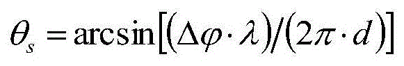
如图1所示,该双结构光栅器件与光学相位调制器件结合构成二维阵列光学相控阵组件,实现激光阵列光源1入射到光学相控阵组件后,通过控制相位调制器件2的各个单元内相邻光束的相位差以及单元间的光束相位差,使得光束经由双结构光栅阵列器件3输出光波的相位在指定的方向上相同,从而实现该方向的相长干涉,同时输出光的相位在其它方向产生相消干涉,从而通过透镜后使光线聚焦到目标扫描位置7处的对应位置,粗光栅的较大结构尺寸与细光栅的微结构尺寸相结合,能够获得大尺寸器件的同时满足作为光学相控阵激光雷达系统中的光束扫描器件的使用功能,而且成本低、工艺简单、使用时可靠性高。通过n× m个透光单元形成一个激光面阵组件,通过控制驱动各激光二极管出射光的相位和强度从而实现面阵组件出射光的方向扫描和照射强度控制,应用于诸如激光雷达、激光测距等场合;如图4所示,具体使用时,粗光栅的每个透光孔对应一个独立的激光二极管器件的光束,相邻透光孔间激光二极管器件的光束相位差为ΔΦ,出射光偏转角度。As shown in Figure 1, the dual-structure grating device and the optical phase modulation device are combined to form a two-dimensional array optical phased array component, and after the laser array
θs=arcsin[(ΔΦ·λ)/(2π·D)]θ s = arcsin[(ΔΦ·λ)/(2π·D)]
其中,λ为入射光波长,D为相邻调制单元间距(或称粗光栅参数),ΔΦ为相邻单元相位差。控制相位差ΔΦ的大小与正负即可实现方向扫描,对应二维面阵器件而言,控制行间单元的相位差可实现方位扫描、控制列间单元的相位差可实现俯仰扫描、控制聚焦透镜可实现前后聚焦深度变化、控制光开关的开启程度可控制照射强度。Among them, λ is the wavelength of the incident light, D is the distance between adjacent modulation units (or coarse grating parameters), and ΔΦ is the phase difference between adjacent units. Directional scanning can be realized by controlling the magnitude and positive or negative of the phase difference ΔΦ. For a two-dimensional area array device, controlling the phase difference between row units can realize azimuth scanning, and controlling the phase difference between column units can realize pitch scanning and control focus The lens can realize the front and rear focus depth changes, and control the opening degree of the optical switch to control the illumination intensity.
细光栅内部的各光束可以进行类似上述的相位调制,也可以不调制,调制后的整体效果要好于不调制。进行调制时,由相位调制器件控制相邻光束相位差为
其中,λ为入射光波长,d为相邻调制光束间距(或称细光栅参数),

本发明采用粗、细光栅相结合的特殊结构设计来解决激光器阵列集成问题与相位调制单元间距微型化问题,粗光栅参数,以满足多激光器集成、器件安装的难题;细光栅参数,合特殊设计的相位调制器件,实现相位调制单元间距微型化、消除旁瓣、提高效率和精度的难题。The present invention uses a special structural design combining coarse and fine gratings to solve the problem of laser array integration and the miniaturization of the pitch of phase modulation units. The parameters of the coarse grating meet the difficulties of multi-laser integration and device installation; The phase modulation device realizes the miniaturization of phase modulation unit spacing, eliminates side lobes, and improves efficiency and precision.
如图5所示,所述的双层结构液晶光开关阵列2由上、下设置的第一层液晶板28和第二层液晶板29构成,第一层液晶板28的上面依次平行设置有第一定向薄膜17、行扫描电极22、上层玻璃板21和上偏振片27,第一层液晶板28的下面依次平行设置有第二定向薄膜16、行信号电极24和中间玻璃板30;第二层液晶板29极板的上面依次平行设置第三定向薄膜18和列扫描电极23,第二层液晶板29的下面依次平行设置有第四定向薄膜19、列信号电极25、下层玻璃板20和下偏振片31;所述的行信号电极24和列信号电极25分别连接有电极引出线26,所述的电极引出线26用于使引出管脚布设合理、方便行信号电极24 和列信号电极25分别与行扫描电极22和列扫描电极23接线在同一个水平面,便于与驱动控制电路相连接控制行信号电极24和列信号电极25通电;所述的行扫描电极22有n个,n个行扫描电极均匀分为n1组,每个组内行扫描电极有n2 个,则n=n1*n2;组内电极宽度与间隔呈等尺寸分布,每组宽度与间隔呈等尺寸分布;As shown in Figure 5, the described double-layer structure liquid crystal
本发明中的中间玻璃板30为双面电极极板,即第一层液晶板28与第二层液晶29板共用的玻璃板,在实际使用中也可以采用两个玻璃板分别加工对应的电极实现,但是明显不如共用一个玻璃板节省成本,共用玻璃板即可在玻璃板的上下两个端面同时设置对应的电极,一体加工。The
所述的列扫描电极23有m个,m个列扫描电极均匀分为m1组,每个组内列扫描电极有m2个,则m=m1*m2;组内电极宽度与间隔呈等尺寸分布,每组宽度与间隔呈等尺寸分布;There are m
n1组行扫描电极对应n3个行信号电极,m1组列扫描电极对应m3个列信号电极,其中n、n1、n2、m、m1、m2、n3、m3均为正整数。The n1 group of row scanning electrodes corresponds to n3 row signal electrodes, and the m1 group of column scanning electrodes corresponds to m3 column signal electrodes, wherein n, n1, n2, m, m1, m2, n3 and m3 are all positive integers.
行扫描电极22与行信号电极24相互垂直且上下覆盖对齐,列信号电极25 与行信号电极24相互垂直且上下覆盖对齐,列扫描电极23与列信号电极25相互垂直且上下覆盖对齐;即由于为垂直关系,所以相互必须都要对应,即不能有行扫描电极22的部分下面没有与其对应的行信号电极24的部分,反之不能有行信号电极24的部分上面没有与其对应的行扫描电极22的部分;列扫描电极23 与列信号电极25存在同样关系,由此构成双层结构光开关控制方法的多样性特征。The
所述的第一定向薄膜17、第二定向薄膜16、第三定向薄膜18和第四定向薄膜19均是由一薄层高分子有机物,经定向摩擦处理,使棒状液晶分子平行于玻璃表面,沿定向处理的方向排列,用于使每一层液晶板的晶体上表面的分子取向与晶体下表面的分子取向相互垂直。所述液晶分子的取向逐渐扭曲,从液晶上表面到下表面扭曲了90°,所以称为扭曲向列相型液晶板。上偏振片27的偏振方向与第一层液晶板28晶体的上表面分子取向相同,第二层液晶板29晶体的上表面分子取向与第一层液晶板28晶体上表面分子取向保持平行,下偏振片31的偏振方向与上偏振片27的偏振方向保持一致。The first oriented
所有电极均处于低电平时,光束入射上偏振片27后,经过上偏振片27形成与第一层液晶板28表面分子取向相同的线偏振光,入射第一层液晶板28,偏振方向随液晶分子长轴旋转90°,以垂直于第二层液晶板29上表面分子取向的线偏振光射出,故光线无法通过第二层液晶板29层,即阵元处于“断”状态;行扫描和列扫描电极均通电且电位高于特定阈值、对应的信号极接地时,光束入射上偏振片后,经过偏振片形成与第一层液晶板28表面分子取向相同的线偏振光,入射第一层液晶板28,由于电场作用光的偏振方向在第一层液晶板28中传播时不再旋转而保持不变,以平行于第二层液晶板29上表面分子取向的线偏振光射出,同样原理,光线通过第二层液晶板29层后出射光线偏振方向原偏振方向平行,可通过下偏振片实现光出射,即阵元处于“通”状态。When all electrodes are at low level, after the light beam is incident on the
所述的光开关扫描控制装置包括保持电路、选通电路、光开关选通控制器和独立可控稳压电源;所述的光开关选通控制器的控制输出端连接选通电路的输入端,选通电路的输出端通过保持电路与待控制开关阵列中的电极相连接;所述的独立可控稳压电源用于对保持电路、选通电路和光开关选通控制器等进行供电;所述的保持电路由多个结构相同的保持单元构成,且保持电路包括行/列信号保持电路、列扫描保持电路和行扫描保持电路;所述的选通电路包括由多个结构相同的选通单元构成行/列信号选通电路、列扫描选通电路和行扫描保持电路。The optical switch scanning control device includes a holding circuit, a gating circuit, an optical switch gating controller and an independent controllable voltage stabilized power supply; the control output end of the optical switch gating controller is connected to the input end of the gating circuit , the output end of the gating circuit is connected to the electrode in the switch array to be controlled through the holding circuit; the independent controllable voltage stabilized power supply is used to supply power to the holding circuit, the gating circuit and the optical switch gating controller; the The holding circuit described above is composed of a plurality of holding units with the same structure, and the holding circuit includes a row/column signal holding circuit, a column scanning holding circuit and a row scanning holding circuit; The unit constitutes a row/column signal gating circuit, a column scanning gating circuit and a row scanning holding circuit.
如图6和图7所示,本发明所述所述的激光阵列光源1由n行×m列个阵元 46阵列排布到可扩展框架45上构成,所述的阵元46为单独封装的个体,且阵元46包括压圈54、准直透镜53、调整垫片52、激光二极管51、前置驱动电路 49、插座47、金属外壳48和有机硅胶50,所述的插座47固定在金属外壳48 一端,与前置驱动电路49相连接;其中,光源即激光二极管51、调整垫片52 和准直透镜53组成准直矫正环节,通过调整垫片52的厚度不同进行一定范围的调节;经特别设计的前置驱动电路49具有电源极性识别功能,可自适应连接外部电源,同时交、直流通用。As shown in Fig. 6 and Fig. 7, the laser array
阵元46将激光二极管51、前置驱动电路49和准直透镜53独立封装为一个单体,阵列不受阵列形式与阵元多少的限制,使得对应的工作模式、扫描、矫正等控制方法相对独立且易于实现不同技术路线的实施,使得阵列整体性能受个别阵元特性的影响降到最低。The
所述的激光二极管51为热沉封装的激光二极管,热沉封装的激光二极管固定在金属外壳48内中间位置,热沉封装的激光二极管的管脚与前置驱动电路49 的输出端连接且通过有机硅胶50灌封;准直透镜分别通过调整垫片和压圈固定设置在金属外壳内的另一端;Described
所述的可扩展框架内包括有平行设置的上固定隔板41、下固定隔板42,n 行×m列个阵元46竖直阵列排布在上、下固定隔板之间,阵元46之间相互平行,且插座端在下端,阵元之间的间隔均匀一致,且间隔内填充有灌封材料43,所述的灌封材料43为铝粉与硅胶的混合物,填充的同时也对阵列46光源整体进行封装;如图6所示,阵元46与外界电路的连接采用接插件47,接插件47包括电源两个电极和控制信号一个电极,经特殊设计的电源极性自动识别电路可自适应连接外部电源,无连接极性对错之忧(不分正、负极),交、直流供电通用,且接地线可在阵列内部通联,故阵元可采用三线制或二线制与外部电路连接。三线制连接时,输入电源为直流恒压源,作为半导体激光二极管的驱动电源;半导体激光二极管的亮度由亮度调节信号独立控制,通过改变亮度调节信号的占空比或频率控制场效应开关管的通/断调节激光亮度。The expandable frame includes an upper fixed
二线制连接时,亮度调节信号无效(接地),输入电源为幅值可变直流电压源,电压的通断控制半导体激光二极管的通断;电源电压幅值的大小调控半导体激光二极管的亮度。When the two-wire system is connected, the brightness adjustment signal is invalid (grounded), and the input power supply is a variable-amplitude DC voltage source, and the on-off of the voltage controls the on-off of the semiconductor laser diode;
图6所示为激光阵列光源组成示意图,所述一种用于光学扫描的激光阵列光源,利用目前的普通半导体激光二极管器件制作成可应用于光学相控阵激光雷达的分布式激光源,采用阵元独立封装、控制;阵元由上下金属隔板固定后封装在可扩展金属框架内,填充硅胶密封;阵列封装金属框架开设有半工字形导槽,多个阵列可通过工字形锁扣方面、快速的组成不同形式、大小的阵列组件,适用于不同的应用要求。Figure 6 is a schematic diagram of the composition of a laser array light source. The laser array light source used for optical scanning is made into a distributed laser source that can be applied to an optical phased array laser radar by using the current common semiconductor laser diode device. The array element is packaged and controlled independently; the array element is fixed by the upper and lower metal partitions and then encapsulated in the expandable metal frame, filled with silicone sealant; the metal frame of the array packaging is provided with a half-shaped guide groove, and multiple arrays can pass through the I-shaped lock. , Quickly form array components of different shapes and sizes, suitable for different application requirements.
所述激光阵列光源的一项突出特点是,阵元将发光体、前置驱动和准直修正独立封装为一个单体,不受阵列形式与阵元多少的限制,使得对应的工作模式、扫描、矫正等控制方法相对独立且易于实现不同技术路线的实施,不受阵元特性的影响。方便、可扩展封装框架也是激光阵列光源的特征之一,在采用阵元独立封装的基础上,封装框架的扩展连接是产品适用性的重要指标,设计采用沿封装外表面下缘开设环形内置半工字型贯通型导槽,在需要拼接扩展时将相向对接的两个阵列模块,利用工字型锁扣连接固定,既不受拼接扩展形式的限制,又不增加辅助元件与难度,正真实现了阵列扩展等同于简单的器件并联应用。A prominent feature of the laser array light source is that the array element independently packages the illuminant, pre-driver and collimation correction into a single unit, which is not limited by the array form and the number of array elements, so that the corresponding working mode, scanning , Correction and other control methods are relatively independent and easy to implement different technical routes, and are not affected by the characteristics of the array elements. The convenient and expandable packaging frame is also one of the characteristics of the laser array light source. On the basis of the independent packaging of the array elements, the expansion connection of the packaging frame is an important indicator of product applicability. The I-shaped through-type guide groove, when splicing and expansion is required, the two array modules that are opposite to each other are connected and fixed by the I-shaped lock. It is not limited by the splicing and expansion form, and does not increase auxiliary components and difficulty. The realization of array expansion is equivalent to simple parallel application of devices.
如图8所示,所述的驱动电路包括滤波电路和驱动与亮度控制电路,所述的滤波电路的输入端连接插座的输出端,滤波电路输出端连接驱动与亮度控制电路的输入端,驱动与亮度控制电路的输出端连接激光二极管的对应管脚。所述的驱动电路还包括有电源极性变换电路,所述的电源极性变换电路为整流模块,用于将不同极性直流电或交流电转换成确定极性的直流电,作为后续电路的电源。所述的滤波电路包括前置滤波和后置滤波,分别设置在整流模块的输入端和输出端,所述的前置滤波和后置滤波均采用电容滤波。所述的驱动与亮度控制电路包括基准电压、比较器、偏置电阻R1、标定电阻R2、限流电阻R3和场效应管,用于依据外部控制信号对激光二极管载荷进行启、闭控制与亮度调节控制。As shown in Figure 8, the drive circuit includes a filter circuit and a drive and brightness control circuit, the input end of the filter circuit is connected to the output end of the socket, the output end of the filter circuit is connected to the input end of the drive and brightness control circuit, and the drive The corresponding pin of the laser diode is connected with the output end of the brightness control circuit. The drive circuit also includes a power supply polarity conversion circuit, which is a rectification module for converting direct current or alternating current of different polarities into direct current with a certain polarity, which is used as a power supply for subsequent circuits. The filter circuit includes a pre-filter and a post-filter, which are respectively arranged at the input end and the output end of the rectification module, and both the pre-filter and the post-filter adopt capacitor filtering. The drive and brightness control circuit includes a reference voltage, a comparator, a bias resistor R1, a calibration resistor R2, a current-limiting resistor R3 and a field effect tube, which are used to control the laser diode load on and off and brightness according to an external control signal. Regulatory control.
前置驱动电路由插座、前滤波、极性变换、后滤波、基准电压、比较器、偏置、反馈、标定、场效应高速开关管和载荷(激光二极管)组成,整流电路输入端与前滤波并联后接插座电源输入插针,极性变换电路输出端与后滤波并联后向后续电路供电;基准电压芯片的输入端接插座亮度调节插针,输出接比较器的参考电压输入端,比较器的输出接场效应高速开关管控制极控制开关的通/断,实现半导体激光二极管通/断、以及亮度的调节,此外还包括偏置、反馈、标定和限流电路。前端通过插座与外部电路连接,后端输出直接驱动半导体激光二极管。经插座输入的电源经C1滤波后输入整流模块(相当于前述的极性变换)的输入端,整流模块的输出端经C2滤波后为比较器和半导体激光二极管供电。外部的亮度调节信号经插座接基准电压模块的输入端,基准电压模块的输出端接比较器的电压参考端,作为亮度控制的基准,比较器的输出端接场效应开关管的栅极,控制场效应开关管的通/断,实现半导体激光二极管通、断控制与亮度调节。上述整流环节在此具有电源极性自调整(也称自适应)功能,使得外部电源无需判别正、负极,可直接接入(无论加在整流模块输入端的电源极性是上正、下负,还是上负、下正,整流模块输出端加载C2上的电压极性依然为上正、下负,后续电路任然正常工作),同时适用于交流供电。The pre-drive circuit is composed of socket, pre-filter, polarity conversion, post-filter, reference voltage, comparator, bias, feedback, calibration, field effect high-speed switch tube and load (laser diode), and the rectifier circuit input terminal and pre-filter Connect the socket power input pin after parallel connection, the output terminal of the polarity conversion circuit is connected in parallel with the post-filtering circuit to supply power to the subsequent circuit; the input terminal of the reference voltage chip is connected to the brightness adjustment pin of the socket, and the output terminal is connected to the reference voltage input terminal of the comparator, and the comparator The output of the field effect high-speed switching tube controls the on/off of the switch to realize the on/off of the semiconductor laser diode and the adjustment of the brightness, and also includes bias, feedback, calibration and current limiting circuits. The front end is connected to the external circuit through the socket, and the output of the back end directly drives the semiconductor laser diode. The power input through the socket is filtered by C1 and then input to the input terminal of the rectification module (equivalent to the aforementioned polarity conversion), and the output terminal of the rectification module is filtered by C2 to supply power for the comparator and the semiconductor laser diode. The external brightness adjustment signal is connected to the input terminal of the reference voltage module through the socket, and the output terminal of the reference voltage module is connected to the voltage reference terminal of the comparator as a reference for brightness control. The output terminal of the comparator is connected to the gate of the field effect switch tube to control The on/off of the field effect switch tube realizes the on/off control and brightness adjustment of the semiconductor laser diode. The above-mentioned rectification link has the function of self-adjustment (also called self-adaptive) of power supply polarity, so that the external power supply does not need to distinguish positive and negative poles, and can be directly connected (regardless of whether the polarity of the power supply applied to the input terminal of the rectification module is upper positive or lower negative, It is still upper negative and lower positive, and the voltage polarity loaded on C2 at the output end of the rectifier module is still upper positive and lower negative, and the subsequent circuit still works normally), and it is also suitable for AC power supply.
n×m激光阵列光源对应于具有n×m个通光窗口的光开关阵列,以及具有n ×m个粗光栅阵元的双结构光栅阵列器件,一个光源阵元与一个光开关通光窗口和一个双结构光栅阵列的粗光栅阵元组成一个微型光学相控阵照射通道,n×m 个微型光学相控阵照射通道按照一定顺序、相位差协同工作,形成整体的基于光学相控阵技术的激光雷达扫描照射工作模式,目标对照射激光的反射信号由雪崩光电二极管器件接收并由微控制器解算相关信息参数。The n×m laser array light source corresponds to an optical switch array with n×m light-through windows, and a double-structure grating array device with n×m coarse grating array elements, one light source element and one optical switch light-through window and The coarse grating elements of a double-structure grating array form a micro-optical phased array illumination channel, and n×m micro-optical phased-array illumination channels work together in a certain order and with a phase difference to form an overall optical phased-array technology-based In the scanning irradiation mode of the laser radar, the reflected signal of the target to the irradiation laser is received by the avalanche photodiode device and the relevant information parameters are solved by the microcontroller.
相邻微型光学相控阵照射通道间,前通道的最后调制光束与后通道的首调制光束间的相位差需要严格的控制,依据扫描工作模式,由开关扫描控制装置进行控制,根据相邻通道器件的间隔尺寸以及在该尺寸方向上光开关扫描电极的宽度,计算出前通道的最后调制光束与后通道的首调制光束间的相位差,由控制器产生延时控制信号进行调节,以实现所有微型光学相控阵照射通道间的相位差一致性的要求。Between adjacent micro-optical phased array irradiation channels, the phase difference between the last modulated beam of the front channel and the first modulated beam of the rear channel needs to be strictly controlled. According to the scanning working mode, it is controlled by the switch scanning control device. According to the adjacent channel The interval size of the device and the width of the optical switch scanning electrode in the dimension direction calculate the phase difference between the last modulated beam of the front channel and the first modulated beam of the rear channel, and the controller generates a delay control signal for adjustment to realize all Requirements for phase difference consistency between illumination channels of micro-optical phased arrays.
双结构光栅阵列器件由粗、细光栅双重结构组成,粗光栅的每个透光单元分别对应于激光照射阵列的一个光束(一个激光二极管发出的一束激光),其效果是将传统的基于光学相控阵激光雷达对单光束的相位调制变为对激光阵列多光束的调制,突破了对阵列单元的尺寸必须不大于500nm(对应于激光波长1微米左右)的限制,使得可以利用常规的材料、加工技术和工艺制作出应用于光学相控阵中进行相位调制的器件;上述每个透光单元又是一个细光栅阵列,与传统器件类似,其光栅参数取决于激光波长,对单束激光进行相关控制,粗、细光栅结合的效果是制作器件的材料易得,微结构加工要求大为降低,制作工艺、设备要求简化,器件的适用性获得极大的提升。The double-structure grating array device is composed of coarse and fine grating double structures. Each light-transmitting unit of the coarse grating corresponds to a beam of laser irradiation array (a beam of laser light emitted by a laser diode). The phase modulation of a single beam of phased array lidar is changed to the modulation of multiple beams of a laser array, which breaks through the limitation that the size of the array unit must not be greater than 500nm (corresponding to a laser wavelength of about 1 micron), making it possible to use conventional materials , processing technology and process to produce a device for phase modulation in an optical phased array; each of the above-mentioned light-transmitting units is a fine grating array, similar to traditional devices, and its grating parameters depend on the laser wavelength. For a single beam of laser The effect of the combination of coarse and fine gratings is that the materials for making devices are easy to obtain, the requirements for microstructure processing are greatly reduced, the requirements for manufacturing processes and equipment are simplified, and the applicability of devices is greatly improved.
所述具有双层结构的液晶光开关阵列,与普通的单层结构的液晶光开关阵列在应用方式与效果上有本质的差别,不同于传统液晶光开关逐行(或列)选通时的“选通→关断→选通→…”脉冲工作模式,而是采用“选通→保持→选通→保持→选通→…”顺序选通并保持工作模式,所以具有类似于窗帘开闭过程的逐渐打开效果。The liquid crystal light switch array with a double-layer structure is essentially different from the liquid crystal light switch array with a common single-layer structure in application mode and effect, and is different from the traditional liquid crystal light switch when gating row by row (or column). "Gating→Off→Gating→..." pulse working mode, but adopts "strobing→holding→strobing→maintaining→strobing→..." sequential strobing and keeping working mode, so it has a similar function to the opening and closing of curtains The gradual opening effect of the process.
利用目前的普通半导体激光二极管器件制作成可应用于光学相控阵激光雷达的分布式激光源,采用阵元独立封装、控制;阵元由上下金属隔板固定后封装在可扩展金属框架内,填充密封;阵列封装金属可扩展框架开设有半工字形导槽,多个阵列可通过工字形锁扣方式快速的组成不同形式、大小的阵列组件,适用于不同的应用要求。The current common semiconductor laser diode device is used to make a distributed laser source that can be applied to optical phased array lidar, and the array elements are independently packaged and controlled; the array elements are fixed by upper and lower metal partitions and then packaged in an expandable metal frame. Filling and sealing; the metal expandable frame of the array packaging is provided with a semi-I-shaped guide groove, and multiple arrays can be quickly formed into array components of different shapes and sizes through the I-shaped locking method, which is suitable for different application requirements.
图9所示,光开关选通(扫描)控制装置,由行/列信号控制电路、行/列扫描控制电路、独立可控高精度稳压电源、光开关选通控制器、以及内置控制代码组成,行/列信号控制电路由行/列信号选通电路和行/列信号保持电路组成,行/ 列扫描控制电路由行/列扫描选通电路和行/列扫描保持电路组成,行/列信号控制电路、行/列扫描控制电路和光开关选通控制器分别由独立可控高精度稳压电源提供不同的工作电压,在光开关选通控制器统一协调下由行/列信号控制电路和行/列扫描控制电路配合负责线性扫描、扇形扫描控制;由独立可控高精度稳压电源配合负责照射强度控制。As shown in Figure 9, the optical switch gating (scanning) control device consists of a row/column signal control circuit, a row/column scanning control circuit, an independently controllable high-precision regulated power supply, an optical switch gating controller, and a built-in control code The row/column signal control circuit is composed of the row/column signal gate circuit and the row/column signal hold circuit. The row/column scan control circuit is composed of the row/column scan gate circuit and the row/column scan hold circuit. The column signal control circuit, the row/column scanning control circuit and the optical switch gating controller are respectively provided with different working voltages by independent controllable high-precision regulated power supplies, and the row/column signal control circuit is controlled by the optical switch gating controller under the unified coordination It cooperates with the row/column scanning control circuit to control the linear scanning and sector scanning; the independent controllable high-precision regulated power supply is responsible for the control of the irradiation intensity.
如图10所示,行/列信号选通电路和行/列扫描选通电路采用高速CMOS多通道模拟多路复用器/多路解复用器集成电路芯片构成,行/列信号保持电路和行/ 列扫描保持电路由集成运放搭建构成,选通电路与保持电路配合,在控制器的控制下,实现通道的“选通”→“保持”→“选通”→…循环。As shown in Figure 10, the row/column signal gating circuit and the row/column scanning gating circuit are composed of high-speed CMOS multi-channel analog multiplexer/demultiplexer integrated circuit chips, and the row/column signal holding circuit And the row/column scanning and holding circuit is composed of integrated operational amplifiers. The strobing circuit cooperates with the holding circuit. Under the control of the controller, the "strobe"→"hold"→"strobe"→...cycle of the channel is realized.
不同的选通(扫描)工作模式对驱动信号的要求不同,针对线形扫描、扇形扫描和深度聚焦3种选通(扫描)工作模式,设计对应的驱动信号特征与时序要求如下:Different gating (scanning) working modes have different requirements for driving signals. For the three gating (scanning) working modes of linear scanning, sectoral scanning and deep focusing, the corresponding driving signal characteristics and timing requirements are as follows:
①线形扫描:延时时间一定或规则变化,驱动信号幅值一定,诸元素逐项通选,任意时刻只能有一个元素选通。①Linear scanning: The delay time is constant or changes regularly, the driving signal amplitude is constant, all elements are selected one by one, and only one element can be selected at any time.
②扇形扫描:延时时间依扇扫规则变化,驱动信号幅值一定,诸元素逐项选通,前期选通的元素后续保持选通。②Sector scan: The delay time changes according to the sector scan rule, the amplitude of the driving signal is constant, all elements are selected one by one, and the elements selected in the previous period remain selected.
③照射强度控制:延时时间规则变化,驱动信号幅值按规则变化,诸元素逐项选通,前期选通的元素后续保持选通。③Irradiation intensity control: The delay time changes regularly, the driving signal amplitude changes according to the rules, all elements are gated one by one, and the elements gated in the previous period remain gated.
图5所示双层结构液晶光开关阵列,所述双层结构液晶光开关阵列,常断状态时,上、下层所有电极处于低电平,全部阵元(通光窗口)处于光遮断状态,在行扫描(或列扫描)工作模式时,置行信号(或列信号)电极A、B、C、D、E…等为低电平、同时置包含列扫描(或行扫描)电极的另一层所有单元(包括该层的所有8×8个通光窗口,以及窗口内的所有10×10个光通道)处于导通状态,然后按照一定时间间隔顺序(对应于相位)逐次置行扫描(或列扫描)电极a、 b、c、d、e、f、…等为高电平,使得对应单元的上、下层液晶在电场作用下光传输沿轴向不再发生扭曲而透光,实现类似于窗帘开闭过程的逐渐打开。经过液晶光开关阵列控制(调制)的光束之间具有一定的相位差(延时),该过程即为光束的相位调制过程,也称为光学相位控制过程。所述具有双层结构的液晶光开关阵列,与普通的单层结构的液晶光开关阵列在应用方式与效果上有本质的差别,不同于传统液晶光开关逐行(或列)选通时的“选通→关断→选通→…”脉冲工作模式,而是采用“选通→保持→选通→保持→选通→…”顺序选通并保持工作模式,所以具有类似于窗帘开闭过程的逐渐打开效果。The double-layer structure liquid crystal optical switch array shown in Fig. 5, when described double-layer structure liquid crystal optical switch array, when normally off state, all electrodes of upper and lower layers are in low level, and all array elements (optical windows) are in light-blocking state, In the row scanning (or column scanning) working mode, set the row signal (or column signal) electrodes A, B, C, D, E...etc. All units on one layer (including all 8×8 optical windows of this layer, and all 10×10 optical channels in the window) are in the conduction state, and then line-scanned sequentially according to a certain time interval (corresponding to the phase) (or column scanning) electrodes a, b, c, d, e, f, ... etc. are at high level, so that the light transmission of the upper and lower liquid crystals of the corresponding unit is no longer twisted in the axial direction under the action of the electric field and transmits light. Realize the gradual opening similar to the curtain opening and closing process. There is a certain phase difference (delay) between the beams controlled (modulated) by the liquid crystal optical switch array. This process is the phase modulation process of the beams, also known as the optical phase control process. The liquid crystal light switch array with a double-layer structure is essentially different from the liquid crystal light switch array with a common single-layer structure in application mode and effect, and is different from the traditional liquid crystal light switch when gating row by row (or column). "Gating→Off→Gating→..." pulse working mode, but adopts "strobing→holding→strobing→maintaining→strobing→..." sequential strobing and keeping working mode, so it has a similar function to the opening and closing of curtains The gradual opening effect of the process.
以下将对本发明的优先实施例进行详细的描述;应当理解,优先实施例仅为了说明本发明,而不是为了限制本发明的保护范围。The preferred embodiments of the present invention will be described in detail below; it should be understood that the preferred embodiments are only for illustrating the present invention, rather than limiting the protection scope of the present invention.
系统光源采用8×8激光阵列光源。输入控制环节,选择小间距3线插座 (ZH1.0-3P);电压极性变换环节,选择快速整流集成芯片(MP6908GJ PD),取 C1=C2=0.22μF;驱动与亮度控制环节,基准电压电路选择LM1403,比较器选择LM358,高速开关电路选择2SJ461场效应管P沟道-50V-100mA,R1=1k, R2=R3=51Ω;载荷驱动环节,选择980nm波长的激光二极管(GH系列),外径3.3mm,长度8.27mm,驱动电压≦3.0V,输出功率120mW。准直透镜透镜采用模造玻璃非球面透镜,直径3.0mm,焦距2.0mm。The system light source adopts 8×8 laser array light source. For the input control link, choose a small-pitch 3-wire socket (ZH1.0-3P); for the voltage polarity conversion link, choose a fast rectification integrated chip (MP6908GJ PD), and take C1=C2=0.22μF; for the drive and brightness control link, the reference voltage The circuit selects LM1403, the comparator selects LM358, the high-speed switch circuit selects 2SJ461 FET P-channel-50V-100mA, R1=1k, R2=R3=51Ω; for the load driving link, select a laser diode with a wavelength of 980nm (GH series), The outer diameter is 3.3mm, the length is 8.27mm, the driving voltage is ≦3.0V, and the output power is 120mW. Collimating lens The lens adopts a molded glass aspheric lens with a diameter of 3.0mm and a focal length of 2.0mm.
相位调制采用8×8双层结构液晶光开关阵列。阵元尺寸为2mm×2mm,阵元间隔2mm,外形与尺寸长×宽×厚为18.5mm×18.5mm×0.5mm。基本参数如下:Phase modulation adopts 8×8 double-layer liquid crystal light switch array. The size of the array element is 2mm×2mm, the interval between the array elements is 2mm, and the shape and size are 18.5mm×18.5mm×0.5mm in length×width×thickness. The basic parameters are as follows:
①行扫描电极外形与尺寸:长方形条状电极,共8组(n1=8),组间间隔 2mm。每组10条电极(n2=10),电极间间隔100μm。共计80条(n=80),每条电极尺寸长×宽×厚为14mm×100μm×150nm。① The shape and size of the line scanning electrodes: rectangular strip electrodes, 8 groups in total (n1=8), with an interval of 2 mm between groups. There are 10 electrodes in each group (n2=10), and the interval between electrodes is 100 μm. There are 80 electrodes in total (n=80), and the size of each electrode is 14 mm×100 μm×150 nm in length×width×thickness.
②行信号电极外形与尺寸:长方形条状电极8条(n3=8),条间间隔2mm,每条电极尺寸长×宽×厚为14mm×2mm×150nm。②Shape and size of row signal electrodes: 8 rectangular strip electrodes (n3=8), the interval between strips is 2mm, and the size of each electrode is 14mm×2mm×150nm in length×width×thickness.
③列扫描电极外形与尺寸:长方形条状电极,共8组(m1=8),组间间隔 2mm。每组10条电极(m2=10),电极间间隔100μm。共计80条(m=80),每条电极尺寸长×宽×厚为14mm×100μm×150nm。③Shape and size of column scanning electrodes: rectangular strip electrodes, 8 groups in total (m1=8), with an interval of 2mm between groups. There are 10 electrodes in each group (m2=10), and the interval between electrodes is 100 μm. There are 80 electrodes in total (m=80), and the size of each electrode is 14 mm×100 μm×150 nm in length×width×thickness.
④列信号电极外形与尺寸:长方形条状电极8条(m3=8),条间间隔2mm,每条电极尺寸长×宽×厚为14mm×2mm×150nm。④ Shape and size of column signal electrodes: 8 rectangular strip electrodes (m3=8), the interval between the strips is 2mm, and the size of each electrode is 14mm×2mm×150nm in length×width×thickness.
光开关选通(扫描)控制装置电路设计采用4套4×4双层结构液晶光开关控制电路,对8×8双层结构液晶光开关阵列进行串、并控制。每套选用5片高速16路复用电路CD74HC4067作为行、列选通(扫描)电路,1片8路复用电路 CD74HC4051作为行、列信号电极控制电路,22片4运放MAX419搭建保持电路,光开关选通(扫描)控制器采用32位ARMCortex-M3结构的STM32F107。单套控制电路原理如图11所示。The circuit design of the optical switch gating (scanning) control device adopts 4 sets of 4×4 double-layer structure liquid crystal light switch control circuits, and performs serial and parallel control on the 8×8 double-layer structure liquid crystal light switch array. Each set uses 5 pieces of high-speed 16-way multiplexing circuit CD74HC4067 as the row and column gating (scanning) circuit, 1 piece of 8-way multiplexing circuit CD74HC4051 as the row and column signal electrode control circuit, and 22 pieces of 4 op amps MAX419 to build the holding circuit. The optical switch gating (scanning) controller adopts STM32F107 with 32-bit ARMCortex-M3 structure. The principle of a single control circuit is shown in Figure 11.
光栅器件器件采用8×8双结构光栅阵列器件,参见图2和图3。基本参数如下:The grating device adopts an 8×8 double-structure grating array device, see Fig. 2 and Fig. 3 . The basic parameters are as follows:
①细光栅:目前常用的激光光源的波长约λ=1μm,考虑消除副瓣应满足 d<λ、提高效率和精度应满足d<<λ等因素,取a=100nm,b=100nm, d=200nm。①Fine grating: The wavelength of the commonly used laser light source is about λ=1μm. Considering the elimination of side lobes, d<λ should be satisfied, and d<<λ should be satisfied to improve efficiency and precision. Take a=100nm, b=100nm, d= 200nm.
②粗光栅:考虑目前激光器件封装尺寸外径最小在4mm左右,取A=2mm, B=2mm,D=A+B=2+2=4mm,对应于激光二极管器件外径尺寸应小于D, 否则器件无法安装、定位,本发明应用例选则激光二极管器件外径尺寸为φ3.5mm。②Coarse grating: Considering that the outer diameter of the current laser device package is at least about 4mm, take A=2mm, B=2mm, D=A+B=2+2=4mm, corresponding to the outer diameter of the laser diode device should be smaller than D, Otherwise, the device cannot be installed and positioned. The outer diameter of the laser diode device is φ3.5mm in the application example of the present invention.
所以,在A=2mm的正方形透光栅格内,均匀排列分布明暗相间的结构,如图3所示为局部放大图。透光孔为直径等于a=100nm的圆形(孔径越小,衍射效果越好),两透光孔间隔为b=100nm。在2mm×2mm范围内均匀分布着 10000×10000=1×10⁸个透光圆孔,形成纵向光栅与横向光栅相结合的面栅结构。Therefore, in the square light-transmitting grid with A=2mm, the light and dark structures are evenly arranged and distributed, as shown in FIG. 3 , which is a partially enlarged view. The light-transmitting hole is a circle with a diameter equal to a=100nm (the smaller the aperture, the better the diffraction effect), and the distance between the two light-transmitting holes is b=100nm. 10000×10000=1×10 8 light-transmitting round holes are evenly distributed within the range of 2mm×2mm, forming a surface grating structure in which longitudinal gratings and horizontal gratings are combined.
③外形尺寸与材质:根据粗光栅的结构尺寸,双结构光栅外形尺寸长×宽×厚确定为32mm×32mm×4mm,材质选用光学K9玻璃。③ Dimensions and materials: According to the structural dimensions of the coarse grating, the outer dimensions of the double-structure grating are determined to be 32mm×32mm×4mm in length×width×thickness, and the material is made of optical K9 glass.
激光反射信号处理装置如图1中的5所示,由采用铟镓砷(InGaAs)雪崩二极管阵列探测器和微控制器组成,光谱波长范围0.9~1.7μm,有效接收面积 4mm×38.5mm,带宽1G、1.5G、2.5G可选,纳秒级响应,短波可扩展到 400nm~1800nm,12V电源供电。The laser reflection signal processing device is shown as 5 in Figure 1. It is composed of InGaAs (InGaAs) avalanche diode array detector and microcontroller. 1G, 1.5G, 2.5G optional, nanosecond response, short wave can be extended to 400nm ~ 1800nm, 12V power supply.
光学系统选择。选用长焦距准直透镜作为照射透镜,短焦距聚焦透镜作为接收透镜。Optical system selection. A collimating lens with a long focal length is selected as the illuminating lens, and a focusing lens with a short focal length is used as the receiving lens.
本发明所述一种光学相控阵激光雷达装置,由激光阵列光源、双层结构液晶光开关阵列、光开关扫描控制装置、双结构光栅阵列器件、激光反射信号处理装置、光学透镜组6部分组成,激光阵列作为系统的照射光源提供平面阵列分布的多光束、平行激光束,双层结构液晶光开关阵列和光开关选通(扫描)控制装置通过光开关的延时选通对光束之间以及光束本身进行相关相位调制,双结构光栅阵列器件利用其特有的衍射嵌套与空间同步干涉特性产生各种转向角度、以及距离方向深度聚焦可调的远场照射模式,对目标进行光学相控阵扫描照射,激光阵列的激光二极管阵元、液晶光开关阵列的通光窗口阵元(本身又是一个阵列)以及双结构光栅阵列粗光栅的阵元(本身也是一个阵列)其数量、间隔尺寸一一对应且保持一致,激光反射信号处理装置对目标反射回来的激光信号进行接收、处理并解算出距离、方位、速度等信息参数,系统配置的扫描照射透镜和目标反射接收透镜对出射光束和入射光束进行矫正。An optical phased array laser radar device according to the present invention consists of six parts: a laser array light source, a double-layer structure liquid crystal optical switch array, an optical switch scanning control device, a double-structure grating array device, a laser reflection signal processing device, and an optical lens group. The laser array is used as the irradiation light source of the system to provide multi-beams and parallel laser beams distributed in a planar array. The double-layer structure liquid crystal optical switch array and the optical switch gating (scanning) control device pass the time-delay gating of the optical switch between the beams and The beam itself undergoes relative phase modulation, and the double-structure grating array device uses its unique diffraction nesting and space synchronization interference characteristics to generate various steering angles and far-field illumination modes with adjustable depth focus in the distance direction, and performs optical phased array on the target. Scanning irradiation, the laser diode array element of the laser array, the optical window array element of the liquid crystal optical switch array (itself is an array) and the array element of the double-structure grating array coarse grating (itself also an array), the number and interval size are the same One-to-one correspondence and consistency, the laser reflection signal processing device receives and processes the laser signal reflected back from the target, and calculates the information parameters such as distance, orientation, speed, etc. The beam is corrected.
Claims (10)
Priority Applications (1)
| Application Number | Priority Date | Filing Date | Title |
|---|---|---|---|
| CN201811219546.0A CN109444903B (en) | 2018-10-18 | 2018-10-18 | An optical phased array laser radar device |
Applications Claiming Priority (1)
| Application Number | Priority Date | Filing Date | Title |
|---|---|---|---|
| CN201811219546.0A CN109444903B (en) | 2018-10-18 | 2018-10-18 | An optical phased array laser radar device |
Publications (2)
| Publication Number | Publication Date |
|---|---|
| CN109444903A CN109444903A (en) | 2019-03-08 |
| CN109444903B true CN109444903B (en) | 2022-11-25 |
Family
ID=65546950
Family Applications (1)
| Application Number | Title | Priority Date | Filing Date |
|---|---|---|---|
| CN201811219546.0A Expired - Fee Related CN109444903B (en) | 2018-10-18 | 2018-10-18 | An optical phased array laser radar device |
Country Status (1)
| Country | Link |
|---|---|
| CN (1) | CN109444903B (en) |
Families Citing this family (13)
| Publication number | Priority date | Publication date | Assignee | Title |
|---|---|---|---|---|
| JP7548590B2 (en) * | 2019-03-25 | 2024-09-10 | セプトン テクノロジーズ,インコーポレイテッド | Mounting configurations for optoelectronic components in lidar systems |
| US12117606B2 (en) * | 2019-08-27 | 2024-10-15 | SCREEN Holdings Co., Ltd. | MEMs phased-array for LiDAR applications |
| CN110783431A (en) * | 2019-11-13 | 2020-02-11 | 中国电子科技集团公司第四十四研究所 | Fabrication method of APD array device |
| CN111722241B (en) * | 2020-05-18 | 2023-09-05 | 深圳奥锐达科技有限公司 | Multi-line scanning distance measuring system, method and electronic equipment |
| CN111579066B (en) * | 2020-06-15 | 2025-11-25 | 深圳市灵明光子科技有限公司 | Photoelectric detection unit, photoelectric detection component and laser ranging device |
| CN114280575B (en) * | 2020-09-27 | 2025-11-11 | 北京万集科技股份有限公司 | Laser radar optical chip based on micro-ring optical switch network |
| CN114152932A (en) * | 2021-11-18 | 2022-03-08 | 苏州迷塔科技有限公司 | System and method for helping opa phased array laser radar eliminate sidelobe signal interference |
| CN114740617B (en) * | 2022-04-08 | 2023-06-30 | 中国科学院光电技术研究所 | Large-view-field high-resolution all-solid-state optical scanning system |
| CN115065406B (en) * | 2022-06-20 | 2023-10-20 | 电子科技大学 | Array multi-beam parallel wireless laser communication system and method |
| CN115167057A (en) * | 2022-06-22 | 2022-10-11 | 电子科技大学 | Transmission-type two-dimensional liquid crystal spatial light modulator |
| CN115128573B (en) * | 2022-08-30 | 2022-12-06 | 北京摩尔芯光半导体技术有限公司 | Drive circuit and drive method for optical phased array and laser radar device |
| CN116500583B (en) * | 2023-03-24 | 2024-04-16 | 扬州群发换热器有限公司 | Laser scanning control system based on optical phased array |
| CN116671980B (en) * | 2023-05-30 | 2024-12-27 | 无锡海斯凯尔医学技术有限公司 | Blood supply information extraction method, device, equipment and readable storage medium |
Citations (6)
| Publication number | Priority date | Publication date | Assignee | Title |
|---|---|---|---|---|
| US5151814A (en) * | 1987-08-19 | 1992-09-29 | Hughes Aircraft Company | Phased array for optical beam control |
| CN103576399A (en) * | 2013-09-26 | 2014-02-12 | 西安空间无线电技术研究所 | Liquid crystal optics phased-array antenna implementation method |
| CN103645470A (en) * | 2013-12-24 | 2014-03-19 | 哈尔滨工业大学 | Double-electric-control scanning laser phased array radar |
| CN204479750U (en) * | 2015-02-06 | 2015-07-15 | 浙江大学 | A kind of light-operated phase battle array radar system based on Wavelength routing |
| WO2017113094A1 (en) * | 2015-12-29 | 2017-07-06 | 浙江大学 | Radar system based on array waveguide grating router |
| WO2018186471A1 (en) * | 2017-04-06 | 2018-10-11 | 国立大学法人横浜国立大学 | Light deflection device |
Family Cites Families (3)
| Publication number | Priority date | Publication date | Assignee | Title |
|---|---|---|---|---|
| US7302179B2 (en) * | 2003-11-17 | 2007-11-27 | Novx Systems, Inc. | Optical performance monitor using co-located switchable fiber bragg grating array |
| CN102354056A (en) * | 2011-10-27 | 2012-02-15 | 中国科学院上海光学精密机械研究所 | High-power high light beam quality optical phased array scanning device |
| WO2018176972A1 (en) * | 2017-04-01 | 2018-10-04 | 北科天绘(苏州)激光技术有限公司 | Laser radar device and channel gating method thereof |
-
2018
- 2018-10-18 CN CN201811219546.0A patent/CN109444903B/en not_active Expired - Fee Related
Patent Citations (6)
| Publication number | Priority date | Publication date | Assignee | Title |
|---|---|---|---|---|
| US5151814A (en) * | 1987-08-19 | 1992-09-29 | Hughes Aircraft Company | Phased array for optical beam control |
| CN103576399A (en) * | 2013-09-26 | 2014-02-12 | 西安空间无线电技术研究所 | Liquid crystal optics phased-array antenna implementation method |
| CN103645470A (en) * | 2013-12-24 | 2014-03-19 | 哈尔滨工业大学 | Double-electric-control scanning laser phased array radar |
| CN204479750U (en) * | 2015-02-06 | 2015-07-15 | 浙江大学 | A kind of light-operated phase battle array radar system based on Wavelength routing |
| WO2017113094A1 (en) * | 2015-12-29 | 2017-07-06 | 浙江大学 | Radar system based on array waveguide grating router |
| WO2018186471A1 (en) * | 2017-04-06 | 2018-10-11 | 国立大学法人横浜国立大学 | Light deflection device |
Non-Patent Citations (4)
| Title |
|---|
| 《Optical phased array technology》;P. F. McManamon et al.;《Proceedings of the IEEE》;19960229;268-298 * |
| 《分布反馈光纤激光器传感阵列关键技术研究》;刘文;《中国博士学位论文全文数据库信息科技辑》;20171115;I135-19 * |
| 《液晶光学相控阵激光雷达中边瓣压缩的研究》;于淼;《中国优秀硕士学位论文全文数据库 信息科技辑》;20140415;I136-525 * |
| 《相控阵激光雷达波控技术的研究与应用》;孙洋东;《中国优秀硕士学位论文全文数据库 信息科技辑》;20110715;I136-709 * |
Also Published As
| Publication number | Publication date |
|---|---|
| CN109444903A (en) | 2019-03-08 |
Similar Documents
| Publication | Publication Date | Title |
|---|---|---|
| CN109444903B (en) | An optical phased array laser radar device | |
| KR101748106B1 (en) | Optoelectronic module with improved optical system | |
| CN111103739B (en) | An electrically controlled variable-focus plane lens | |
| KR100654004B1 (en) | Ray deflector and scanner | |
| US12305817B2 (en) | Light-emitting apparatus using metasurfaces and light-emitting method thereof | |
| US20080271784A1 (en) | Electro-optic prism systems | |
| US20090250094A1 (en) | Method and system for light ray concentration | |
| CN109188823B (en) | A laser array light source for optical scanning | |
| KR20220116323A (en) | TOF depth sensing module and image creation method | |
| CN113126061B (en) | Laser radar and scanning method thereof | |
| KR20100047875A (en) | Color conversion device and color controllable light-output device | |
| US4577052A (en) | AC Solar cell | |
| EP3754247A1 (en) | Illumination device | |
| US11290055B2 (en) | Optical light-transmission element for a solar energy assembly comprising a harvesting portion and an alignment control portion, and method for alignment of such | |
| WO2022118074A1 (en) | Method and apparatus for electrical power generation | |
| US10690323B2 (en) | Target-oriented light emitting device, and optical module | |
| CN206832985U (en) | A kind of all-solid state laser radar installations | |
| US20120180847A1 (en) | Method for improving solar energy condensation efficiency in solar energy condensation electric power facility | |
| CN109343027B (en) | A laser radar multi-dimensional scanning control device and control method | |
| CN103208950A (en) | Off-axis Fresnel reflection condenser-based concentrating photovoltaic power generation device | |
| ES2956835B2 (en) | LIGHTING DEVICE AND SPECTRAL MODULATOR | |
| RU2522656C2 (en) | Luminaire | |
| Mazur et al. | Modelling of 3D solar module based on flexible photovoltaic panels | |
| SU1576802A2 (en) | Orientation photosensor | |
| CN204129395U (en) | Based on the infrared waves bundle control chip of electrically-controlled liquid crystal infrared convergence plane microtrabeculae mirror |
Legal Events
| Date | Code | Title | Description |
|---|---|---|---|
| PB01 | Publication | ||
| PB01 | Publication | ||
| SE01 | Entry into force of request for substantive examination | ||
| SE01 | Entry into force of request for substantive examination | ||
| GR01 | Patent grant | ||
| GR01 | Patent grant | ||
| CF01 | Termination of patent right due to non-payment of annual fee |
Granted publication date: 20221125 |
|
| CF01 | Termination of patent right due to non-payment of annual fee |