CN109309100B - Thin film transistor, gate drive circuit and display panel - Google Patents
Thin film transistor, gate drive circuit and display panel Download PDFInfo
- Publication number
- CN109309100B CN109309100B CN201811149006.XA CN201811149006A CN109309100B CN 109309100 B CN109309100 B CN 109309100B CN 201811149006 A CN201811149006 A CN 201811149006A CN 109309100 B CN109309100 B CN 109309100B
- Authority
- CN
- China
- Prior art keywords
- thin film
- sub
- film transistor
- film transistors
- active layer
- Prior art date
- Legal status (The legal status is an assumption and is not a legal conclusion. Google has not performed a legal analysis and makes no representation as to the accuracy of the status listed.)
- Active
Links
Images


Classifications
-
- G—PHYSICS
- G09—EDUCATION; CRYPTOGRAPHY; DISPLAY; ADVERTISING; SEALS
- G09G—ARRANGEMENTS OR CIRCUITS FOR CONTROL OF INDICATING DEVICES USING STATIC MEANS TO PRESENT VARIABLE INFORMATION
- G09G5/00—Control arrangements or circuits for visual indicators common to cathode-ray tube indicators and other visual indicators
- G09G5/003—Details of a display terminal, the details relating to the control arrangement of the display terminal and to the interfaces thereto
-
- H—ELECTRICITY
- H10—SEMICONDUCTOR DEVICES; ELECTRIC SOLID-STATE DEVICES NOT OTHERWISE PROVIDED FOR
- H10D—INORGANIC ELECTRIC SEMICONDUCTOR DEVICES
- H10D86/00—Integrated devices formed in or on insulating or conducting substrates, e.g. formed in silicon-on-insulator [SOI] substrates or on stainless steel or glass substrates
- H10D86/40—Integrated devices formed in or on insulating or conducting substrates, e.g. formed in silicon-on-insulator [SOI] substrates or on stainless steel or glass substrates characterised by multiple TFTs
-
- H—ELECTRICITY
- H10—SEMICONDUCTOR DEVICES; ELECTRIC SOLID-STATE DEVICES NOT OTHERWISE PROVIDED FOR
- H10D—INORGANIC ELECTRIC SEMICONDUCTOR DEVICES
- H10D30/00—Field-effect transistors [FET]
- H10D30/60—Insulated-gate field-effect transistors [IGFET]
- H10D30/67—Thin-film transistors [TFT]
- H10D30/6729—Thin-film transistors [TFT] characterised by the electrodes
- H10D30/673—Thin-film transistors [TFT] characterised by the electrodes characterised by the shapes, relative sizes or dispositions of the gate electrodes
-
- H—ELECTRICITY
- H10—SEMICONDUCTOR DEVICES; ELECTRIC SOLID-STATE DEVICES NOT OTHERWISE PROVIDED FOR
- H10D—INORGANIC ELECTRIC SEMICONDUCTOR DEVICES
- H10D30/00—Field-effect transistors [FET]
- H10D30/60—Insulated-gate field-effect transistors [IGFET]
- H10D30/67—Thin-film transistors [TFT]
- H10D30/6757—Thin-film transistors [TFT] characterised by the structure of the channel, e.g. transverse or longitudinal shape or doping profile
-
- H—ELECTRICITY
- H10—SEMICONDUCTOR DEVICES; ELECTRIC SOLID-STATE DEVICES NOT OTHERWISE PROVIDED FOR
- H10D—INORGANIC ELECTRIC SEMICONDUCTOR DEVICES
- H10D86/00—Integrated devices formed in or on insulating or conducting substrates, e.g. formed in silicon-on-insulator [SOI] substrates or on stainless steel or glass substrates
- H10D86/40—Integrated devices formed in or on insulating or conducting substrates, e.g. formed in silicon-on-insulator [SOI] substrates or on stainless steel or glass substrates characterised by multiple TFTs
- H10D86/421—Integrated devices formed in or on insulating or conducting substrates, e.g. formed in silicon-on-insulator [SOI] substrates or on stainless steel or glass substrates characterised by multiple TFTs having a particular composition, shape or crystalline structure of the active layer
-
- H—ELECTRICITY
- H10—SEMICONDUCTOR DEVICES; ELECTRIC SOLID-STATE DEVICES NOT OTHERWISE PROVIDED FOR
- H10D—INORGANIC ELECTRIC SEMICONDUCTOR DEVICES
- H10D86/00—Integrated devices formed in or on insulating or conducting substrates, e.g. formed in silicon-on-insulator [SOI] substrates or on stainless steel or glass substrates
- H10D86/40—Integrated devices formed in or on insulating or conducting substrates, e.g. formed in silicon-on-insulator [SOI] substrates or on stainless steel or glass substrates characterised by multiple TFTs
- H10D86/441—Interconnections, e.g. scanning lines
-
- H—ELECTRICITY
- H10—SEMICONDUCTOR DEVICES; ELECTRIC SOLID-STATE DEVICES NOT OTHERWISE PROVIDED FOR
- H10D—INORGANIC ELECTRIC SEMICONDUCTOR DEVICES
- H10D86/00—Integrated devices formed in or on insulating or conducting substrates, e.g. formed in silicon-on-insulator [SOI] substrates or on stainless steel or glass substrates
- H10D86/40—Integrated devices formed in or on insulating or conducting substrates, e.g. formed in silicon-on-insulator [SOI] substrates or on stainless steel or glass substrates characterised by multiple TFTs
- H10D86/60—Integrated devices formed in or on insulating or conducting substrates, e.g. formed in silicon-on-insulator [SOI] substrates or on stainless steel or glass substrates characterised by multiple TFTs wherein the TFTs are in active matrices
-
- H—ELECTRICITY
- H10—SEMICONDUCTOR DEVICES; ELECTRIC SOLID-STATE DEVICES NOT OTHERWISE PROVIDED FOR
- H10H—INORGANIC LIGHT-EMITTING SEMICONDUCTOR DEVICES HAVING POTENTIAL BARRIERS
- H10H20/00—Individual inorganic light-emitting semiconductor devices having potential barriers, e.g. light-emitting diodes [LED]
- H10H20/80—Constructional details
- H10H20/81—Bodies
- H10H20/816—Bodies having carrier transport control structures, e.g. highly-doped semiconductor layers or current-blocking structures
-
- G—PHYSICS
- G09—EDUCATION; CRYPTOGRAPHY; DISPLAY; ADVERTISING; SEALS
- G09G—ARRANGEMENTS OR CIRCUITS FOR CONTROL OF INDICATING DEVICES USING STATIC MEANS TO PRESENT VARIABLE INFORMATION
- G09G2300/00—Aspects of the constitution of display devices
- G09G2300/04—Structural and physical details of display devices
- G09G2300/0421—Structural details of the set of electrodes
- G09G2300/0426—Layout of electrodes and connections
-
- G—PHYSICS
- G09—EDUCATION; CRYPTOGRAPHY; DISPLAY; ADVERTISING; SEALS
- G09G—ARRANGEMENTS OR CIRCUITS FOR CONTROL OF INDICATING DEVICES USING STATIC MEANS TO PRESENT VARIABLE INFORMATION
- G09G2310/00—Command of the display device
- G09G2310/02—Addressing, scanning or driving the display screen or processing steps related thereto
- G09G2310/0264—Details of driving circuits
Landscapes
- Engineering & Computer Science (AREA)
- Physics & Mathematics (AREA)
- Computer Hardware Design (AREA)
- General Physics & Mathematics (AREA)
- Theoretical Computer Science (AREA)
- Thin Film Transistor (AREA)
- Liquid Crystal (AREA)
Abstract
本发明的实施例公开了薄膜晶体管、栅极驱动电路和显示面板。该薄膜晶体管包括:衬底基板,设置在衬底基板上的梳齿形状的栅极、有源层、位于栅极和有源层之间的栅极绝缘层、以及梳齿形状的源电极和漏电极。源电极的第一齿部和漏电极的第二齿部沿第一方向交替设置,并且在衬底基板上的正投影与有源层分别至少部分重叠。栅极的第三齿部位于邻近的第一齿部和第二齿部之间。有源层与第三齿部在衬底基板上的正投影相交的区域为第一相交部。第一齿部、第二齿部、第三齿部以及有源层形成多个并联的子薄膜晶体管。多个子薄膜晶体管中在中心位置处的至少一个中心子薄膜晶体管的第一相交部在第一方向上的第一尺寸与该第一相交部在第二方向上的第二尺寸的比值最大,其中,第二方向与第一方向垂直。

Embodiments of the present invention disclose a thin film transistor, a gate driving circuit and a display panel. The thin film transistor comprises: a base substrate, a comb-shaped gate electrode, an active layer, a gate insulating layer located between the gate electrode and the active layer, a comb-shaped source electrode and a comb-shaped source electrode arranged on the base substrate. drain electrode. The first teeth of the source electrode and the second teeth of the drain electrode are alternately arranged along the first direction, and the orthographic projections on the base substrate at least partially overlap with the active layer, respectively. The third tooth portion of the grid is located between the adjacent first tooth portion and the second tooth portion. The region where the active layer intersects with the orthographic projection of the third tooth portion on the base substrate is the first intersecting portion. The first tooth portion, the second tooth portion, the third tooth portion and the active layer form a plurality of sub-thin film transistors connected in parallel. The ratio of the first dimension of the first intersection in the first direction to the second dimension of the first intersection in the second direction of at least one central sub-thin film transistor at the central position in the plurality of sub-thin film transistors is the largest, wherein , the second direction is perpendicular to the first direction.
Description
技术领域technical field
本发明涉及显示技术领域,具体地,涉及薄膜晶体管、栅极驱动电路和显示面板。The present invention relates to the field of display technology, in particular, to a thin film transistor, a gate driving circuit and a display panel.
背景技术Background technique
目前,显示面板的窄边框化已成为趋势。在显示面板中,可采用将栅极驱动电路整合到阵列基板上的技术实现,即GOA(Gate Driver On Array)技术。在GOA技术中,通常需要具有超大宽长比的薄膜晶体管来实现大电流,以保证显示面板的显示效果。在现有技术中,具有超大宽长比的薄膜晶体管一般采用由多个子薄膜晶体管并联形成的梳状薄膜晶体管。At present, the narrow border of the display panel has become a trend. In the display panel, the technology of integrating the gate driving circuit on the array substrate, that is, the GOA (Gate Driver On Array) technology can be adopted. In the GOA technology, a thin film transistor with an ultra-large aspect ratio is usually required to achieve a large current, so as to ensure the display effect of the display panel. In the prior art, a thin film transistor with a super large aspect ratio generally adopts a comb-shaped thin film transistor formed by paralleling a plurality of sub thin film transistors.
发明内容SUMMARY OF THE INVENTION
本发明的实施例提供了一种薄膜晶体管、相应的栅极驱动电路和显示面板,其能够减少在薄膜晶体管的中心区域积累的热量,从而避免由于中心区域过热而导致的晶体管的击穿现象。Embodiments of the present invention provide a thin film transistor, a corresponding gate driving circuit and a display panel, which can reduce heat accumulated in a central region of the thin film transistor, thereby avoiding transistor breakdown caused by overheating of the central region.
根据本发明的第一方面,提供了一种薄膜晶体管。该薄膜晶体管包括衬底基板、设置于衬底基板上的梳齿形状的栅极、有源层、位于栅极和有源层之间的栅极绝缘层、以及梳齿形状的源电极和漏电极。进一步地,源电极的第一齿部和漏电极的第二齿部沿第一方向交替设置并且在衬底基板上的正投影与有源层分别至少部分重叠。栅极的第三齿部位于邻近的第一齿部和第二齿部之间。有源层与第三齿部在衬底基板上的正投影相交的区域为第一相交部。第一齿部、第二齿部、第三齿部以及有源层形成多个并联的子薄膜晶体管。多个子薄膜晶体管中在中心位置处的至少一个中心子薄膜晶体管的第一相交部在第一方向上的第一尺寸与第一相交部在第二方向上的第二尺寸的比值最大,且第二方向与第一方向垂直。According to a first aspect of the present invention, a thin film transistor is provided. The thin film transistor includes a base substrate, a comb-shaped gate electrode disposed on the base substrate, an active layer, a gate insulating layer between the gate electrode and the active layer, and a comb-shaped source electrode and a drain electrode pole. Further, the first teeth of the source electrode and the second teeth of the drain electrode are alternately arranged along the first direction and the orthographic projections on the base substrate at least partially overlap with the active layer, respectively. The third tooth portion of the grid is located between the adjacent first tooth portion and the second tooth portion. The region where the active layer intersects with the orthographic projection of the third tooth portion on the base substrate is the first intersecting portion. The first tooth portion, the second tooth portion, the third tooth portion and the active layer form a plurality of sub-thin film transistors connected in parallel. The ratio of the first dimension of the first intersection in the first direction to the second dimension of the first intersection in the second direction of at least one central sub-thin film transistor at the central position of the plurality of sub-thin film transistors is the largest, and the The second direction is perpendicular to the first direction.
在本发明的实施例中,多个子薄膜晶体管的相应的第一相交部的第二尺寸相同,并且至少一个中心子薄膜晶体管的第一相交部的第一尺寸最大。In an embodiment of the present invention, the second size of the corresponding first intersections of the plurality of sub-thin film transistors is the same, and the first size of the first intersection of at least one central sub-thin film transistor is the largest.
在本发明的实施例中,多个子薄膜晶体管中不同于至少一个中心子薄膜晶体管的其它子薄膜晶体管的第一相交部的第一尺寸相同。In an embodiment of the present invention, the first size of the first intersection of the other sub-thin film transistors of the plurality of sub-thin film transistors different from the at least one central sub-thin film transistor is the same.
在本发明的实施例中,对于多个子薄膜晶体管中不同于至少一个中心子薄膜晶体管的其它子薄膜晶体管,随着与至少一个中心子薄膜晶体管之间的距离的增加,其它子薄膜晶体管的第一相交部的第一尺寸减小。In the embodiment of the present invention, for other sub-thin film transistors in the plurality of sub-thin film transistors that are different from at least one central sub-thin film transistor, as the distance from the at least one central sub-thin film transistor increases, the first sub-thin film transistor of the other sub-thin film transistors increases. The first dimension of an intersection is reduced.
在本发明的实施例中,有源层在第二方向上被分隔成多个段。In an embodiment of the present invention, the active layer is divided into a plurality of segments in the second direction.
在本发明的实施例中,多个段在第二方向上的尺寸相同。In an embodiment of the invention, the plurality of segments are the same size in the second direction.
在本发明的实施例中,多个段在第二方向上的尺寸不同。In an embodiment of the invention, the plurality of segments differ in size in the second direction.
在本发明的实施例中,多个段中处于中心位置处的至少一个段在第二方向上的尺寸最小。In an embodiment of the present invention, at least one of the plurality of segments at the central position has the smallest dimension in the second direction.
在本发明的实施例中,多个子薄膜晶体管的相应的第一相交部的第一尺寸相同,并且至少一个中心子薄膜晶体管的第一相交部的第二尺寸最小。In an embodiment of the present invention, the first size of the corresponding first intersections of the plurality of sub-thin film transistors is the same, and the second size of the first intersection of the at least one central sub-thin film transistor is the smallest.
在本发明的实施例中,对于多个子薄膜晶体管中不同于至少一个中心子薄膜晶体管的其它子薄膜晶体管的第一相交部的第二尺寸相同。In an embodiment of the present invention, the second dimension of the first intersection for other sub-thin film transistors of the plurality of sub-thin film transistors different from at least one central sub-thin film transistor is the same.
在本发明的实施例中,对于多个子薄膜晶体管中不同于至少一个中心薄膜晶体管的其它子薄膜晶体管,随着与至少一个中心子薄膜晶体管之间的距离的增加,其它子薄膜晶体管的第一相交部的第二尺寸增大。In an embodiment of the present invention, for other sub-thin film transistors different from at least one central thin-film transistor among the plurality of sub-thin-film transistors, as the distance from the at least one central sub-thin film transistor increases, the first sub-thin film transistor of the other sub-thin film transistors increases. The second dimension of the intersection is increased.
在本发明的实施例中,对于多个子薄膜晶体管中的各个子薄膜晶体管,有源层中用于形成该子薄膜晶体管的区域在第二方向上被分隔成多个段。In an embodiment of the present invention, for each sub-thin film transistor in the plurality of sub-thin film transistors, the region in the active layer for forming the sub-thin film transistor is divided into a plurality of segments in the second direction.
在本发明的实施例中,至少一个中心子薄膜晶体管的第一相交部的第一尺寸最大且第二尺寸最小。In an embodiment of the present invention, the first intersection of the at least one central sub-thin film transistor has the largest first dimension and the smallest second dimension.
根据本发明的第二方面,提供了一种栅极驱动电路。该栅极驱动电路包括根据本发明的第一方面所述的薄膜晶体管。According to a second aspect of the present invention, a gate driving circuit is provided. The gate driving circuit includes the thin film transistor according to the first aspect of the present invention.
根据本发明的第三方面,提供了一种阵列基板。该阵列基板包括根据本发明的第二方面所述的栅极驱动电路。According to a third aspect of the present invention, an array substrate is provided. The array substrate includes the gate driving circuit according to the second aspect of the present invention.
根据本发明的第四方面,提供了一种阵列基板。该阵列基板包括根据本发明的第一方面所述的薄膜晶体管。According to a fourth aspect of the present invention, an array substrate is provided. The array substrate includes the thin film transistor according to the first aspect of the present invention.
附图说明Description of drawings
为了更清楚地说明本发明的实施例的技术方案,下面将对实施例的附图进行简要说明,应当知道,以下描述的附图仅仅涉及本发明的一些实施例,而非对本发明的限制,其中,贯穿这些附图的各个视图,相应的参考编号指示相应的部件或特征:In order to illustrate the technical solutions of the embodiments of the present invention more clearly, the accompanying drawings of the embodiments will be briefly described below. It should be understood that the drawings described below only relate to some embodiments of the present invention, rather than limit the present invention. Wherein, throughout the various views of the drawings, corresponding reference numerals indicate corresponding parts or features:
图1是现有的示例性梳状薄膜晶体管的平面示意图;FIG. 1 is a schematic plan view of an existing exemplary comb-shaped thin film transistor;
图2是根据本发明的第一实施例的薄膜晶体管的平面示意图;2 is a schematic plan view of a thin film transistor according to a first embodiment of the present invention;
图3是根据本发明的第二实施例的薄膜晶体管的平面示意图;3 is a schematic plan view of a thin film transistor according to a second embodiment of the present invention;
图4是根据本发明的第三实施例的薄膜晶体管的平面示意图;4 is a schematic plan view of a thin film transistor according to a third embodiment of the present invention;
图5是根据本发明的第四实施例的薄膜晶体管的平面示意图;5 is a schematic plan view of a thin film transistor according to a fourth embodiment of the present invention;
图6是根据本发明的第五实施例的薄膜晶体管的平面示意图;6 is a schematic plan view of a thin film transistor according to a fifth embodiment of the present invention;
图7是根据本发明的第六实施例的薄膜晶体管的平面示意图;7 is a schematic plan view of a thin film transistor according to a sixth embodiment of the present invention;
图8是根据本发明的第七实施例的薄膜晶体管的平面示意图;8 is a schematic plan view of a thin film transistor according to a seventh embodiment of the present invention;
图9是根据本发明的第八实施例的薄膜晶体管的平面示意图;9 is a schematic plan view of a thin film transistor according to an eighth embodiment of the present invention;
图10是根据本发明的第九实施例的薄膜晶体管的平面示意图;10 is a schematic plan view of a thin film transistor according to a ninth embodiment of the present invention;
图11是根据本发明的第十实施例的薄膜晶体管的平面示意图;11 is a schematic plan view of a thin film transistor according to a tenth embodiment of the present invention;
图12是根据本发明的第十一实施例的薄膜晶体管的平面示意图;12 is a schematic plan view of a thin film transistor according to an eleventh embodiment of the present invention;
图13是根据本发明的实施例的栅极驱动电路的示意性框图;以及13 is a schematic block diagram of a gate drive circuit according to an embodiment of the present invention; and
图14是根据本发明的实施例的显示面板的示意性框图。14 is a schematic block diagram of a display panel according to an embodiment of the present invention.
具体实施方式Detailed ways
为了使本发明的实施例的目的、技术方案和优点更加清楚,下面将结合附图,对本发明的实施例的技术方案进行清楚、完整的描述。显然,所描述的实施例是本发明的一部分实施例,而不是全部的实施例。基于所描述的本发明的实施例,本领域技术人员在无需创造性劳动的前提下所获得的所有其他实施例,也都属于本发明保护的范围。In order to make the objectives, technical solutions and advantages of the embodiments of the present invention clearer, the technical solutions of the embodiments of the present invention will be described clearly and completely below with reference to the accompanying drawings. Obviously, the described embodiments are some, but not all, embodiments of the present invention. Based on the described embodiments of the present invention, all other embodiments obtained by those skilled in the art without creative efforts also fall within the protection scope of the present invention.
当介绍本发明的元素及其实施例时,冠词“一”、“一个”、“该”和“所述”旨在表示存在一个或者多个要素。用语“包含”、“包括”、“含有”和“具有”旨在包括性的并且表示可以存在除所列要素之外的另外的要素。When introducing elements of the present invention and the embodiments thereof, the articles "a," "an," "the," and "said" are intended to mean that there are one or more of the elements. The terms "comprising," "including," "containing," and "having" are intended to be inclusive and mean that there may be additional elements other than the listed elements.
出于下文表面描述的目的,如其在附图中被标定方向那样,术语“上”、“下”、“左”、“右”“垂直”、“水平”、“顶”、“底”及其派生词应涉及发明。术语“上覆”、“在……顶上”、“定位在……上”或者“定位在……顶上”意味着诸如第一结构的第一要素存在于诸如第二结构的第二要素上,其中,在第一要素和第二要素之间可存在诸如界面结构的中间要素。术语“接触”意味着连接诸如第一结构的第一要素和诸如第二结构的第二要素,而在两个要素的界面处可以有或者没有其它要素。For the purposes of the following surface description, the terms "upper", "lower", "left", "right", "vertical", "horizontal", "top", "bottom" and Its derivatives shall refer to inventions. The terms "overlying", "on top of", "positioned on" or "positioned on top of" mean that a first element, such as a first structure, exists on a second element, such as a second structure above, wherein an intermediate element such as an interface structure may exist between the first element and the second element. The term "contacting" means connecting a first element, such as a first structure, and a second element, such as a second structure, with or without other elements at the interface of the two elements.
除非另外定义,否则在此使用的所有术语(包括技术和科学术语)具有与本发明主题所属领域的技术人员所通常理解的相同含义。进一步将理解的是,诸如在通常使用的词典中定义的那些的术语应解释为具有与说明书上下文和相关技术中它们的含义一致的含义,并且将不以理想化或过于正式的形式来解释,除非在此另外明确定义。如在此所使用的,将两个或更多部分“连接”或“耦接”到一起的陈述应指这些部分直接结合到一起或通过一个或多个中间部件结合。Unless otherwise defined, all terms (including technical and scientific terms) used herein have the same meaning as commonly understood by one of ordinary skill in the art to which this inventive subject matter belongs. It will be further understood that terms such as those defined in commonly used dictionaries should be interpreted to have meanings consistent with their meanings in the context of the specification and related art, and will not be interpreted in an idealized or overly formalized form, unless otherwise expressly defined herein. As used herein, the statement that two or more parts are "connected" or "coupled" together shall mean that the parts are joined together directly or through one or more intervening components.
图1示意性地示出了现有的示例性的具有超大宽长比的梳状薄膜晶体管的平面示意图。FIG. 1 schematically shows a schematic plan view of an existing exemplary comb-shaped thin film transistor with an ultra-large aspect ratio.
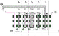
如图1所示,梳状薄膜晶体管可包括衬底基板(未示出)、梳齿形状的栅极101、有源层102、位于栅极和有源层之间的栅极绝缘层(未示出)、以及梳齿形状的源电极103和漏电极104。源电极103的第一齿部(图示为3个)和漏电极104的第二齿部(图示为3个)沿图示的水平方向交替设置。第一齿部和第二齿部在衬底基板上的正投影与有源层102部分重叠以在有源层102上形成源区域和漏区域。栅极101的第三齿部(图示为5个)位于邻近的第一齿部和第二齿部之间。有源层102与第三齿部在衬底基板上的正投影相交的区域(即第一相交部)在有源层102上形成沟道区。这样,第一齿部、第二齿部、第三齿部和有源层102可形成五个并联的子薄膜晶体管T1、T2、T3、T4、T5。在图1所示的薄膜晶体管中,子薄膜晶体管T2与T1共用漏电极104的第一个第二齿部并与T3共用源电极103的第二个第一齿部。子薄膜晶体管T3与T4共用漏电极104的第二个第二齿部。子薄膜晶体管T4与T5共用源电极103的第三个第一齿部。As shown in FIG. 1, the comb-shaped thin film transistor may include a base substrate (not shown), a
另外,在图1的示例中,子薄膜晶体管T1、T2、T3、T4、T5的沟道区的长度(即,第一相交部在水平方向上的尺寸)分别表示为L1、L2、L3、L4、L5,宽度(即,第一相交部在垂直方向上的尺寸)则被分别表示为W1、W2、W3、W4、W5。可见,五个子薄膜晶体管的沟道区的宽度和长度是相同的。In addition, in the example of FIG. 1 , the lengths of the channel regions of the sub-thin film transistors T1, T2, T3, T4, T5 (ie, the dimension of the first intersection in the horizontal direction) are denoted as L1, L2, L3, L4, L5, the width (ie, the dimension of the first intersection in the vertical direction) is then denoted as W1, W2, W3, W4, W5, respectively. It can be seen that the width and length of the channel regions of the five sub-TFTs are the same.
在使用如图1所示的薄膜晶体管的阵列基板中,在阵列基板被提供工作电压进行工作期间,由于工作电压不变,因此,各子薄膜晶体管所产生的热量Q可被计算为Q=U2/R·T,其中,U表示子薄膜晶体管的源极与漏极之间的电压,R表示子薄膜晶体管的沟道区的电阻(由于子薄膜晶体管的其它部件的发热效果不明显,因此,一般仅考虑沟道区的电阻),T表示子薄膜晶体管的工作时间。因此,单位时间内子薄膜晶体管所产生的热量Q与其沟道区的电阻R成反比。而沟道区的电阻R与沟道区的宽长比(W/L)相关,即,宽长比越大,电阻越小。因此,子薄膜晶体管所产生的热量与其宽长比成反比。In the array substrate using the thin film transistor as shown in FIG. 1 , during the operation period when the array substrate is supplied with the operating voltage, since the operating voltage does not change, the heat Q generated by each sub-TFT can be calculated as Q=U 2 /R T, where U represents the voltage between the source and drain of the sub-TFT, and R represents the resistance of the channel region of the sub-TFT (because the heating effect of other components of the sub-TFT is not obvious, so , generally only the resistance of the channel region is considered), T represents the working time of the sub-thin film transistor. Therefore, the heat Q generated by the sub-thin film transistor per unit time is inversely proportional to the resistance R of its channel region. The resistance R of the channel region is related to the width-to-length ratio (W/L) of the channel region, that is, the larger the width-to-length ratio, the smaller the resistance. Therefore, the heat generated by the sub-TFT is inversely proportional to its width-to-length ratio.
在图1的示例中,由于五个子薄膜晶体管的沟道区的宽度和长度相同,因此,所产生的热量也相同。在这种情况下,位于两侧的子薄膜晶体管T1、T2、T4、T5对中间的子薄膜晶体管T3造成热辐射热量增强的作用,这样,薄膜晶体管的中心区域容易由于过热而导致烧毁。In the example of FIG. 1 , since the width and length of the channel regions of the five sub-thin film transistors are the same, the generated heat is also the same. In this case, the sub-thin-film transistors T1, T2, T4, and T5 located on both sides have the effect of enhancing the heat radiation of the sub-thin-film transistor T3 in the middle, so that the central area of the thin-film transistor is easily burnt due to overheating.
为了解决这一技术问题,本发明的实施例提出了一种新型的薄膜晶体管。通过将薄膜晶体管中的在中心位置处的子薄膜晶体管(也称为“中心子薄膜晶体管”)的第一相交部的长度与宽度的比值设置为最大,使得薄膜晶体管中的中心子薄膜晶体管产生的热量最少,从而,避免薄膜晶体管的中心区域由于过热而被烧毁。以下结合附图对根据本发明的实施例的薄膜晶体管进行详细说明。在以下的本发明的实施例中,为了便于说明,薄膜晶体管采用与如图1所示的薄膜晶体管类似的结构,因此,对于相同的部分,适当省略其说明。In order to solve this technical problem, an embodiment of the present invention proposes a novel thin film transistor. By setting the ratio of the length to the width of the first intersection of the sub-thin film transistor at the center position (also referred to as the "center sub-thin film transistor") in the thin-film transistor to be the largest, the center sub-thin-film transistor in the thin-film transistor produces The heat is minimized, thereby preventing the central region of the thin film transistor from being burned due to overheating. The thin film transistors according to the embodiments of the present invention will be described in detail below with reference to the accompanying drawings. In the following embodiments of the present invention, for convenience of description, the thin film transistor adopts a structure similar to that of the thin film transistor shown in FIG. 1 , and therefore, the description of the same parts is appropriately omitted.
图2示出了根据本发明的第一实施例的薄膜晶体管的平面示意图。FIG. 2 shows a schematic plan view of a thin film transistor according to a first embodiment of the present invention.
如图2所示,在本实施例中,薄膜晶体管的子薄膜晶体管T1、T2、T3、T4、T5的沟道区的宽度W1、W2、W3、W4、W5被设置为相同,而作为中心子薄膜晶体管的子薄膜晶体管T3的沟道区的长度L3被设置为最长。As shown in FIG. 2, in this embodiment, the widths W1, W2, W3, W4, W5 of the channel regions of the sub-thin film transistors T1, T2, T3, T4, T5 of the thin film transistor are set to be the same, and the The length L3 of the channel region of the sub thin film transistor T3 of the sub thin film transistor is set to be the longest.
进一步地,其它子薄膜晶体管T1、T2、T4、T5的沟道区的长度L1、L2、L4、L5可被设置为相同,并且小于L3。Further, the lengths L1, L2, L4, L5 of the channel regions of the other sub-thin film transistors T1, T2, T4, T5 may be set to be the same and smaller than L3.
因此,在本实施例中,与子薄膜晶体管T1、T2、T4、T5相比,子薄膜晶体管T3的沟道区的宽长比W3/L3最小,相应地,子薄膜晶体管T3的沟道区的电阻最大。这样,在薄膜晶体管工作期间,子薄膜晶体管T3所产生的热量最小,能够有效避免薄膜晶体管的中心区域由于过热而烧毁。Therefore, in this embodiment, compared with the sub-thin-film transistors T1, T2, T4, and T5, the width-to-length ratio W3/L3 of the channel region of the sub-thin-film transistor T3 is the smallest. Correspondingly, the channel region of the sub-thin-film transistor T3 maximum resistance. In this way, during the operation of the thin film transistor, the heat generated by the sub-thin film transistor T3 is minimal, which can effectively prevent the central region of the thin film transistor from being burned due to overheating.
尽管在本实施例中仅将一个子薄膜晶体管T3的沟道区的长度设置为最长,但本领域中的技术人员可以理解,也可以将位于中心位置处的多个子薄膜晶体管的沟道区的长度设置为最长。例如,也可以将子薄膜晶体管T2、T3、T4的沟道区的长度设置为最长。Although only the length of the channel region of one sub thin film transistor T3 is set to be the longest in this embodiment, those skilled in the art can understand that the channel regions of a plurality of sub thin film transistors located at the central position may also be set to be the longest. The length is set to the longest. For example, the lengths of the channel regions of the sub-thin film transistors T2, T3, and T4 may also be set to be the longest.
图3示出了根据本发明的第二实施例的薄膜晶体管的平面示意图。在本实施例中,除了将子薄膜晶体管T1、T2、T3、T4、T5的沟道区的宽度W1、W2、W3、W4、W5设置为相同以及将子薄膜晶体管T3的沟道区的长度L3设置为最长以外,对于子薄膜晶体管T1、T2、T4、T5,随着与子薄膜晶体管T3之间的距离越大,子薄膜晶体管T1、T2、T4、T5的沟道区的长度L1、L2、L4、L5越小。FIG. 3 shows a schematic plan view of a thin film transistor according to a second embodiment of the present invention. In this embodiment, except that the widths W1, W2, W3, W4, and W5 of the channel regions of the sub thin film transistors T1, T2, T3, T4, and T5 are set to be the same and the length of the channel region of the sub thin film transistor T3 is set to be the same L3 is set to be the longest, for the sub-thin film transistors T1, T2, T4, T5, the length L1 of the channel regions of the sub-thin film transistors T1, T2, T4, T5 increases with the distance from the sub-thin film transistor T3. , L2, L4, and L5 are smaller.
如图3所示,子薄膜晶体管T1和T5距子薄膜晶体管T3较远,子薄膜晶体管T2和T4距子薄膜晶体管T3较近。因此,可将子薄膜晶体管T1、T5的沟道区的长度L1、L5设置为最小,将子薄膜晶体管T2、T4的沟道区的长度L2、L4设置为大于长度L1和L5,而将子薄膜晶体管T3的沟道区的长度L3设置为最大。因此,子薄膜晶体管T3的沟道区的宽长比W3/L3最小,电阻最大,相应地,所产生的热量最小。As shown in FIG. 3 , the sub thin film transistors T1 and T5 are far from the sub thin film transistor T3, and the sub thin film transistors T2 and T4 are relatively close to the sub thin film transistor T3. Therefore, the lengths L1 and L5 of the channel regions of the sub thin film transistors T1 and T5 can be set to the minimum, the lengths L2 and L4 of the channel regions of the sub thin film transistors T2 and T4 can be set to be greater than the lengths L1 and L5, and the The length L3 of the channel region of the thin film transistor T3 is set to be maximum. Therefore, the width-to-length ratio W3/L3 of the channel region of the sub-thin film transistor T3 is the smallest, the resistance is the largest, and accordingly, the heat generated is the smallest.
图4示出了根据本发明的第三实施例的薄膜晶体管的平面示意图。在本实施例中,在图2所示的第一实施例的薄膜晶体管的基础上,进一步将有源层在图示的垂直方向上分隔成宽度相等的三个段。FIG. 4 shows a schematic plan view of a thin film transistor according to a third embodiment of the present invention. In this embodiment, on the basis of the thin film transistor of the first embodiment shown in FIG. 2 , the active layer is further divided into three segments with equal widths in the vertical direction shown in the figure.
如图4所示,薄膜晶体管的有源层202在图示的垂直方向上被分隔成三个段,并且三个段的宽度W11、W12、W13相同。在这种情况下,子薄膜晶体管的沟道区的宽度相同,并且都等于W11、W12与W13的和。因此,子薄膜晶体管T3的沟道区的宽长比W3/L3最小,电阻最大,相应地,所产生的热量最小。As shown in FIG. 4 , the active layer 202 of the thin film transistor is divided into three segments in the vertical direction shown in the figure, and the widths W11 , W12 , and W13 of the three segments are the same. In this case, the widths of the channel regions of the sub-thin film transistors are the same, and are all equal to the sum of W11, W12, and W13. Therefore, the width-to-length ratio W3/L3 of the channel region of the sub-thin film transistor T3 is the smallest, the resistance is the largest, and accordingly, the heat generated is the smallest.
尽管在本实施例中,有源层被分隔成三个段,但本领域中的技术人员可以理解,有源层也可以被分隔成其它数量的段。Although in this embodiment, the active layer is divided into three segments, those skilled in the art can understand that the active layer can also be divided into other numbers of segments.
图5示出了根据本发明的第四实施例的薄膜晶体管的平面示意图。在本实施例中,在图3所示的第二实施例的薄膜晶体管的基础上,进一步将有源层在垂直方向分隔成宽度相等的三个段,并且三个段的宽度W11、W12、W13相同。在这种情况下,子薄膜晶体管的沟道区的宽度相同,并且都等于W11、W12与W13的和。因此,子薄膜晶体管T3的沟道区的宽长比W3/L3最小,电阻最大,相应地,所产生的热量最小。FIG. 5 shows a schematic plan view of a thin film transistor according to a fourth embodiment of the present invention. In this embodiment, on the basis of the thin film transistor of the second embodiment shown in FIG. 3 , the active layer is further divided into three segments with equal widths in the vertical direction, and the widths of the three segments are W11, W12, Same for W13. In this case, the widths of the channel regions of the sub-thin film transistors are the same, and are all equal to the sum of W11, W12, and W13. Therefore, the width-to-length ratio W3/L3 of the channel region of the sub-thin film transistor T3 is the smallest, the resistance is the largest, and accordingly, the heat generated is the smallest.
图6示出了根据本发明的第五实施例的薄膜晶体管的平面示意图。在本实施例中,在图4所示的第三实施例的薄膜晶体管的基础上,进一步将在有源层上处于中心位置的中心段的宽度W12设置为最小,并将其它两个段的宽度W11、W13设置为相同,且大于W12。在这种情况下,子薄膜晶体管的沟道区的宽度相同,并且都等于W11、W12与W13的和。因此,子薄膜晶体管T3的沟道区的宽长比W3/L3最小,电阻最大,相应地,所产生的热量最小。FIG. 6 shows a schematic plan view of a thin film transistor according to a fifth embodiment of the present invention. In this embodiment, on the basis of the thin film transistor of the third embodiment shown in FIG. 4 , the width W12 of the central segment at the center position on the active layer is further set to the minimum, and the width W12 of the other two segments is set to the minimum. The widths W11 and W13 are set to be the same and larger than W12. In this case, the widths of the channel regions of the sub-thin film transistors are the same, and are all equal to the sum of W11, W12, and W13. Therefore, the width-to-length ratio W3/L3 of the channel region of the sub-thin film transistor T3 is the smallest, the resistance is the largest, and accordingly, the heat generated is the smallest.
尽管在本实施例中将在有源层上位于中心位置处的一个中心段的宽度设置为最小,但本领域的技术人员可以理解,也可以将位于中心位置处的多个中心段的宽度设置为最小。例如,在有源层在垂直方向上被分隔成五个段的实施例中,可以将位于中心位置处的三个段的宽度设置为最小。Although the width of one central segment located at the central position on the active layer is set to be the smallest in this embodiment, those skilled in the art can understand that the widths of a plurality of central segments located at the central position can also be set to to the minimum. For example, in an embodiment where the active layer is vertically divided into five segments, the width of the three segments located at the center position may be set to be the smallest.
图7示出了根据本发明的第六实施例的薄膜晶体管的平面示意图。在本实施例中,在图5所示的第四实施例的薄膜晶体管的基础上,进一步将在有源层上位于中心位置处的段的宽度W12设置为最小,并将其它两个段的宽度W11、W13设置为相同,且大于W12。这样的情况下,子薄膜晶体管的沟道区的宽度相同,并且都等于W11、W12与W13的和。因此,子薄膜晶体管T3的沟道区的宽长比W3/L3最小,电阻最大,相应地,所产生的热量最小。FIG. 7 shows a schematic plan view of a thin film transistor according to a sixth embodiment of the present invention. In this embodiment, on the basis of the thin film transistor of the fourth embodiment shown in FIG. 5 , the width W12 of the segment located at the center position on the active layer is further set to the minimum, and the width W12 of the other two segments is set to the minimum. The widths W11 and W13 are set to be the same and larger than W12. In this case, the widths of the channel regions of the sub-thin film transistors are the same and equal to the sum of W11, W12 and W13. Therefore, the width-to-length ratio W3/L3 of the channel region of the sub-thin film transistor T3 is the smallest, the resistance is the largest, and accordingly, the heat generated is the smallest.
图8示出了根据本发明的第七实施例的薄膜晶体管的平面示意图。在本实施例中,子薄膜晶体管T1、T2、T3、T4、T5的沟道区的长度L1、L2、L3、L4、L5被设置为相同,而位于中心位置处的子薄膜晶体管T3的沟道区的宽度W3被设置为最小。FIG. 8 shows a schematic plan view of a thin film transistor according to a seventh embodiment of the present invention. In this embodiment, the lengths L1, L2, L3, L4, and L5 of the channel regions of the sub-thin film transistors T1, T2, T3, T4, and T5 are set to be the same, and the channel regions of the sub-thin film transistor T3 at the center position are set to be the same. The width W3 of the track area is set to be the smallest.
进一步地,子薄膜晶体管T1、T2、T4、T5的沟道区的宽度W1、W2、W4、W5被设置为相同,且大于W3。Further, the widths W1, W2, W4, W5 of the channel regions of the sub-thin film transistors T1, T2, T4, T5 are set to be the same and larger than W3.
因此,在本实施例中,与子薄膜晶体管T1、T2、T4、T5相比,子薄膜晶体管T3的沟道区的宽长比W3/L3最小。相应地,子薄膜晶体管T3的沟道区的电阻最大。这样,在薄膜晶体管工作期间,子薄膜晶体管T3所产生的热量最小,能够有效避免薄膜晶体管的中心区域由于过热而烧毁。Therefore, in this embodiment, compared with the sub-thin-film transistors T1, T2, T4, and T5, the width-to-length ratio W3/L3 of the channel region of the sub-thin-film transistor T3 is the smallest. Accordingly, the resistance of the channel region of the sub thin film transistor T3 is the largest. In this way, during the operation of the thin film transistor, the heat generated by the sub-thin film transistor T3 is minimal, which can effectively prevent the central region of the thin film transistor from being burned due to overheating.
图9示出了根据本发明的第八实施例的薄膜晶体管的平面示意图。在本实施例中,除了将子薄膜晶体管T1、T2、T3、T4、T5的沟道区的长度L1、L2、L3、L4、L5设置为相同以及将子薄膜晶体管T3的沟道区的宽度设置为最小以外,对于子薄膜晶体管T1、T2、T4、T5,随着与子薄膜晶体管T3的距离越大,子薄膜晶体管T1、T2、T4、T5的沟道区的宽度W1、W2、W4、W5越大。FIG. 9 shows a schematic plan view of a thin film transistor according to an eighth embodiment of the present invention. In this embodiment, except that the lengths L1, L2, L3, L4, and L5 of the channel regions of the sub thin film transistors T1, T2, T3, T4, and T5 are set to be the same and the width of the channel region of the sub thin film transistor T3 is set to be the same Set to the minimum value, for the sub-thin film transistors T1, T2, T4, T5, as the distance from the sub-thin film transistor T3 increases, the widths W1, W2, W4 of the channel regions of the sub-thin film transistors T1, T2, T4, T5 , W5 is larger.
如图9所示,子薄膜晶体管T1和T5距子薄膜晶体管T3较远,子薄膜晶体管T2和T4距子薄膜晶体管T3较近。因此,可将子薄膜晶体管T1、T5的沟道区的宽度W1、W5设置为最大,将子薄膜晶体管T2、T4的沟道区的宽度W2、W4设置为小于宽度W1和W5,而将子薄膜晶体管T3的沟道区的宽度W3设置为最小。因此,子薄膜晶体管T3宽长比W3/L3最小,电阻最大,相应地,所产生的热量最小。As shown in FIG. 9 , the sub thin film transistors T1 and T5 are far from the sub thin film transistor T3, and the sub thin film transistors T2 and T4 are relatively close to the sub thin film transistor T3. Therefore, the widths W1 and W5 of the channel regions of the sub thin film transistors T1 and T5 can be set to the maximum, the widths W2 and W4 of the channel regions of the sub thin film transistors T2 and T4 can be set to be smaller than the widths W1 and W5, and The width W3 of the channel region of the thin film transistor T3 is set to be the smallest. Therefore, the sub-thin film transistor T3 has the smallest aspect ratio W3/L3, the largest resistance, and correspondingly, the smallest heat generation.
图10示出了根据本发明的第九实施例的薄膜晶体管的平面示意图。在本实施例中,在图8所示的第七实施例的薄膜晶体管的基础上,进一步将子薄膜晶体管对应的各个有源层区域在图示的垂直方向上分别分隔成五段或四段。FIG. 10 shows a schematic plan view of a thin film transistor according to a ninth embodiment of the present invention. In this embodiment, on the basis of the thin film transistor of the seventh embodiment shown in FIG. 8 , each active layer region corresponding to the sub-thin film transistor is further divided into five sections or four sections in the vertical direction shown in the figure. .
如图10所示,子薄膜晶体管T1、T2、T3、T4、T5对应的有源层的区域的宽度相同。进一步地,通过四个分隔物,将与子薄膜晶体管T3对应的有源层的区域在图示的垂直方向上分隔成五段。并且通过三个分隔物,将与子薄膜晶体管T1、T2、T4、T5对应的有源层的区域分隔成四段。在本发明的实施例中,分隔物的宽度相同,且可以采用与栅极绝缘层相同的材料形成。在这种情况下,子薄膜晶体管T3的沟道区的宽度W3等于有源层的区域的宽度减去四个分隔物的宽度,子薄膜晶体管T1、T2、T4、T5的沟道区的宽度W1、W2、W4、W5等于有源层的区域的宽度减去三个分隔物的宽度,即宽度W1、W2、W4、W5小于W3。因此,子薄膜晶体管T3的沟道区的宽长比W3/L3最小,电阻最大,相应地,所产生的热量最小。As shown in FIG. 10 , the widths of the regions of the active layers corresponding to the sub-thin film transistors T1 , T2 , T3 , T4 and T5 are the same. Further, the region of the active layer corresponding to the sub-thin film transistor T3 is divided into five sections in the vertical direction shown in the figure by four spacers. And the regions of the active layer corresponding to the sub-thin film transistors T1 , T2 , T4 , and T5 are separated into four sections by three spacers. In embodiments of the present invention, the spacers have the same width and may be formed of the same material as the gate insulating layer. In this case, the width W3 of the channel region of the sub thin film transistor T3 is equal to the width of the region of the active layer minus the width of the four spacers, the width of the channel region of the sub thin film transistors T1, T2, T4, T5 W1 , W2 , W4 , W5 are equal to the width of the region of the active layer minus the width of the three spacers, ie the widths W1 , W2 , W4 , W5 are smaller than W3 . Therefore, the width-to-length ratio W3/L3 of the channel region of the sub-thin film transistor T3 is the smallest, the resistance is the largest, and accordingly, the heat generated is the smallest.
可替换地,在本发明的实施例中,与各个子薄膜晶体管对应的有源层的区域的宽度可以不同,分隔物的宽度也可以不同。Alternatively, in the embodiment of the present invention, the widths of the regions of the active layers corresponding to the respective sub-thin film transistors may be different, and the widths of the spacers may also be different.
图11示出了根据本发明的第十实施例的薄膜晶体管的平面示意图。在本实施例中,在图9所示的第八实施例的薄膜晶体管的基础上,进一步将子薄膜晶体管对应的各个有源层区域在图示的垂直方向上分别分隔成五段、四段或三段。FIG. 11 shows a schematic plan view of a thin film transistor according to a tenth embodiment of the present invention. In this embodiment, on the basis of the thin film transistor of the eighth embodiment shown in FIG. 9 , each active layer region corresponding to the sub-thin film transistor is further divided into five sections and four sections in the vertical direction shown in the figure. or three paragraphs.
如图11所示,子薄膜晶体管T1、T2、T3、T4、T5对应的有源层的区域的宽度相同。进一步地,通过四个分隔物,将与子薄膜晶体管T3对应的有源层的区域在图示的垂直方向上分隔成五段。通过三个分隔物,将与子薄膜晶体管T2、T4对应的有源层的区域分隔成四段。并且通过两个分隔物,将与子薄膜晶体管T1、T5对应的有源层的区域分隔成三段。在本发明的实施例中,分隔物的宽度相同,并且分隔物可以采用与栅极绝缘层相同的材料形成。在这种情况下,子薄膜晶体管T3的沟道区的宽度W3等于对应的有源层的区域的宽度减去四个分隔物的宽度,子薄膜晶体管T2、T4的沟道区的宽度W2、W4等于对应的有源层的区域的宽度W2、W4减去三个分隔物的宽度,而子薄膜晶体管T1、T5的沟道区的宽度W1、W5等于对应的有源层的区域的宽度减去两个分隔物的宽度,即宽度W1、W5大于宽度W2、W4,且宽度W2、W4大于宽度W3。因此,子薄膜晶体管T3的沟道区的宽长比W3/L3最小,电阻最大,相应地,所产生的热量最小。As shown in FIG. 11 , the widths of the regions of the active layers corresponding to the sub-thin film transistors T1 , T2 , T3 , T4 and T5 are the same. Further, the region of the active layer corresponding to the sub-thin film transistor T3 is divided into five sections in the vertical direction shown in the figure by four spacers. The regions of the active layer corresponding to the sub-thin film transistors T2 and T4 are divided into four sections by three spacers. And the regions of the active layer corresponding to the sub-thin film transistors T1 and T5 are separated into three sections by two spacers. In embodiments of the present invention, the widths of the spacers are the same, and the spacers may be formed of the same material as the gate insulating layer. In this case, the width W3 of the channel region of the sub-thin film transistor T3 is equal to the width of the corresponding active layer region minus the width of the four spacers, and the widths W2, W4 is equal to the widths W2 and W4 of the corresponding active layer regions minus the widths of the three spacers, while the widths W1 and W5 of the channel regions of the sub-thin film transistors T1 and T5 are equal to the widths of the corresponding active layer regions minus the widths of the three spacers. Go to the width of the two dividers, ie, the widths W1, W5 are larger than the widths W2, W4, and the widths W2, W4 are larger than the width W3. Therefore, the width-to-length ratio W3/L3 of the channel region of the sub-thin film transistor T3 is the smallest, the resistance is the largest, and accordingly, the heat generated is the smallest.
尽管在本发明的一些实施例中,与子薄膜晶体管对应的有源层区域被分别分隔成五段、四段或三段,但本领域中的技术人员可以理解,有源层也可以被分隔成其它数量的段。Although in some embodiments of the present invention, the active layer regions corresponding to the sub-thin film transistors are respectively divided into five, four or three segments, those skilled in the art can understand that the active layer can also be divided into other numbers of segments.
图12示出了根据本发明的第十一实施例的薄膜晶体管的平面示意图。在本实施例中,薄膜晶体管的位于中心位置的子薄膜晶体管T3的沟道区的长度L3被设置为最长,沟道区的宽度W3被设置为最小。FIG. 12 shows a schematic plan view of a thin film transistor according to an eleventh embodiment of the present invention. In this embodiment, the length L3 of the channel region of the sub-thin film transistor T3 at the center position of the thin film transistor is set to be the longest, and the width W3 of the channel region is set to be the smallest.
进一步地,将子薄膜晶体管T1、T2、T4、T5的沟道区L1、L2、L4、L5的长度设置为相同,并且将子薄膜晶体管T1、T2、T4、T5的沟道区的宽度W1、W2、W4、W5设置为相同。Further, the lengths of the channel regions L1, L2, L4, and L5 of the sub thin film transistors T1, T2, T4, and T5 are set to be the same, and the width W1 of the channel regions of the sub thin film transistors T1, T2, T4, and T5 is set , W2, W4, W5 are set to the same.
可替换地,在本发明的实施例中,子薄膜晶体管T1、T2、T4、T5的沟道区的长度L1、L2、L4、L5可以采用与图3所示的实施例相同的设置,即随着与子薄膜晶体管T3之间的距离越大,将子薄膜晶体管T1、T2、T4、T5的沟道区的长度L1、L2、L4、L5设置为越小。Alternatively, in the embodiment of the present invention, the lengths L1, L2, L4, and L5 of the channel regions of the sub-thin film transistors T1, T2, T4, and T5 may adopt the same settings as those in the embodiment shown in FIG. 3, that is, The lengths L1 , L2 , L4 , L5 of the channel regions of the sub thin film transistors T1 , T2 , T4 , T5 are set to be smaller as the distance from the sub thin film transistor T3 is larger.
可替换地,在本发明的实施例中,子薄膜晶体管T1、T2、T4、T5的宽度W1、W2、W4、W5可以采用与图9所示的实施例相同的设置,即随着与子薄膜晶体管T3之间的距离越大,将子薄膜晶体管T1、T2、T4、T5的沟道区的宽度W1、W2、W4、W5设置为越大。Alternatively, in the embodiment of the present invention, the widths W1, W2, W4, and W5 of the sub-thin film transistors T1, T2, T4, and T5 may adopt the same settings as those in the embodiment shown in FIG. The larger the distance between the thin film transistors T3, the larger the widths W1, W2, W4, W5 of the channel regions of the sub thin film transistors T1, T2, T4, T5 are set.
可替换地,在本发明的实施例中,子薄膜晶体管T1、T2、T3、T4、T5的沟道区的宽度W1、W2、W3、W4、W5可以采用与图10所示的实施例相同的设置,即,在与子薄膜晶体管T1、T2、T3、T4、T5对应的有源层的区域的宽度相同的情况下,通过宽度相同的分隔物,将与子薄膜晶体管T3对应的有源层的区域在图示的垂直方向上分隔成五段,将与子薄膜晶体管T1、T2、T4、T5对应的有源层的区域分隔成四段。Alternatively, in the embodiment of the present invention, the widths W1, W2, W3, W4, and W5 of the channel regions of the sub-thin film transistors T1, T2, T3, T4, and T5 may be the same as those in the embodiment shown in FIG. 10 . , that is, in the case where the widths of the regions of the active layers corresponding to the sub-thin film transistors T1, T2, T3, T4, and T5 are the same, the active layer corresponding to the sub-thin film transistor T3 is separated by a spacer with the same width. The region of the layer is divided into five sections in the vertical direction shown in the figure, and the region of the active layer corresponding to the sub-thin film transistors T1, T2, T4, and T5 is divided into four sections.
可替换地,在本发明的实施例中,子薄膜晶体管T1、T2、T3、T4、T5的沟道区的宽度W1、W2、W3、W4、W5可以采用与图11所示的实施例相同的设置,即,在子薄膜晶体管T1、T2、T3、T4、T5对应的有源层的区域的宽度相同的情况下,通过宽度相同的分隔物,将与子薄膜晶体管T3对应的有源层的区域在图示的垂直方向上分隔成五段,将与子薄膜晶体管T2、T4、对应的有源层的区域分隔成四段,并将与子薄膜晶体管T1、T5对应的有源层的区域分隔成三段。Alternatively, in the embodiment of the present invention, the widths W1, W2, W3, W4, and W5 of the channel regions of the sub-thin film transistors T1, T2, T3, T4, and T5 may be the same as those in the embodiment shown in FIG. 11 . , that is, in the case where the widths of the regions of the active layers corresponding to the sub-thin film transistors T1, T2, T3, T4, and T5 are the same, the active layer corresponding to the sub-thin film transistor T3 is separated by a spacer with the same width. The area is divided into five sections in the vertical direction shown in the figure, and the area of the active layer corresponding to the sub-thin film transistors T2, T4 and the corresponding active layer is divided into four sections, and the active layer corresponding to the sub-thin film transistors T1 and T5 The area is divided into three sections.
因此,在本实施例中,与子薄膜晶体管T1、T2、T4、T5相比,子薄膜晶体管T3的沟道区的宽长比W3/L3最小,相应地,子薄膜晶体管T3的沟道区的电阻最大。这样,在薄膜晶体管工作期间,子薄膜晶体管T3所产生的热量最小,能够有效避免薄膜晶体管的中心区域由于过热而烧毁。Therefore, in this embodiment, compared with the sub-thin-film transistors T1, T2, T4, and T5, the width-to-length ratio W3/L3 of the channel region of the sub-thin-film transistor T3 is the smallest. Correspondingly, the channel region of the sub-thin-film transistor T3 maximum resistance. In this way, during the operation of the thin film transistor, the heat generated by the sub-thin film transistor T3 is minimal, which can effectively prevent the central region of the thin film transistor from being burned due to overheating.
此外,根据上述实施例的薄膜晶体管可在栅极驱动电路或像素电路中使用,以实现大电流,同时避免击穿。In addition, the thin film transistors according to the above-described embodiments can be used in gate driving circuits or pixel circuits to achieve large currents while avoiding breakdown.
图13示出了根据本发明的实施例的栅极驱动电路1300的示意性框图。如图13所示,栅极驱动电路1300可包括如图2至图12任一所示的薄膜晶体管1200。FIG. 13 shows a schematic block diagram of a
图14示出了根据本发明的实施例的阵列基板1400的示意性框图。如图14所示,阵列基板1400可包括上述的如图13所示的栅极驱动电路1300。在其它实施例中,阵列基板1400可包括如图2至图12任一所示的薄膜晶体管1200。根据本发明的实施例的阵列基板1400可以用于任何具有显示功能的产品或部件。这样的产品或部件包括但不限于显示装置、可穿戴设备、移动电话、平板电脑、电视机、笔记本电脑、数码相框、导航仪等。FIG. 14 shows a schematic block diagram of an
尽管在以上实施例中薄膜晶体管采用五个子薄膜晶体管并联形成,但本领域的技术人员可以理解,本发明的实施例的薄膜晶体管中也可以采用其它数量的子薄膜晶体管并联形成。Although the thin film transistors in the above embodiments are formed by using five sub thin film transistors in parallel, those skilled in the art can understand that other numbers of sub thin film transistors can also be formed in parallel in the thin film transistors of the embodiments of the present invention.
以上已经描述了根据本发明的若干实施例,这些实施例仅通过举例的方式展现,而且不旨在限制本发明的范围。事实上,本文所描述的新颖实施例也可以以各种其它形式来实施。此外,在不脱离本发明的精神下,可以对本文所描述的实施例的形式进行各种省略、替代和改变。所附权利要求以及它们的等价物旨在覆盖落在本发明范围和精神内的此类形式或者修改。Several embodiments in accordance with the present invention have been described above, these embodiments have been presented by way of example only, and are not intended to limit the scope of the invention. Indeed, the novel embodiments described herein may also be embodied in various other forms. Furthermore, various omissions, substitutions and changes in the form of the embodiments described herein may be made without departing from the spirit of the inventions. The appended claims and their equivalents are intended to cover such forms or modifications as fall within the scope and spirit of the inventions.
Claims (18)
Priority Applications (3)
| Application Number | Priority Date | Filing Date | Title |
|---|---|---|---|
| CN201811149006.XA CN109309100B (en) | 2018-09-29 | 2018-09-29 | Thin film transistor, gate drive circuit and display panel |
| US16/493,429 US11183142B2 (en) | 2018-09-29 | 2019-05-06 | Thin film transistor, gate driver circuit and display apparatus |
| PCT/CN2019/085710 WO2020062871A1 (en) | 2018-09-29 | 2019-05-06 | Thin film transistor, gate driver circuit and display apparatus |
Applications Claiming Priority (1)
| Application Number | Priority Date | Filing Date | Title |
|---|---|---|---|
| CN201811149006.XA CN109309100B (en) | 2018-09-29 | 2018-09-29 | Thin film transistor, gate drive circuit and display panel |
Publications (2)
| Publication Number | Publication Date |
|---|---|
| CN109309100A CN109309100A (en) | 2019-02-05 |
| CN109309100B true CN109309100B (en) | 2020-12-29 |
Family
ID=65225304
Family Applications (1)
| Application Number | Title | Priority Date | Filing Date |
|---|---|---|---|
| CN201811149006.XA Active CN109309100B (en) | 2018-09-29 | 2018-09-29 | Thin film transistor, gate drive circuit and display panel |
Country Status (3)
| Country | Link |
|---|---|
| US (1) | US11183142B2 (en) |
| CN (1) | CN109309100B (en) |
| WO (1) | WO2020062871A1 (en) |
Families Citing this family (16)
| Publication number | Priority date | Publication date | Assignee | Title |
|---|---|---|---|---|
| CN109309100B (en) | 2018-09-29 | 2020-12-29 | 京东方科技集团股份有限公司 | Thin film transistor, gate drive circuit and display panel |
| US11189704B2 (en) * | 2019-06-10 | 2021-11-30 | Tcl China Star Optofi Fctronics Technology Co.. Ltd. | Thin film transistor and electrical circuit |
| CN110289309B (en) * | 2019-06-10 | 2021-04-27 | Tcl华星光电技术有限公司 | Thin film transistor and circuit |
| CN111312805B (en) * | 2019-11-01 | 2021-07-06 | 深圳市华星光电半导体显示技术有限公司 | Thin film transistor structure, GOA circuit and display device |
| CN114270431B (en) * | 2020-06-04 | 2023-06-02 | 京东方科技集团股份有限公司 | Display substrate, manufacturing method and display device |
| CN113823696B (en) | 2020-06-18 | 2024-08-20 | 京东方科技集团股份有限公司 | Thin film transistor, manufacturing method thereof, display substrate and display device |
| CN116504791A (en) * | 2020-06-28 | 2023-07-28 | 京东方科技集团股份有限公司 | Thin film transistor, gate row driving circuit and array substrate |
| CN114512510A (en) * | 2020-11-16 | 2022-05-17 | 群创光电股份有限公司 | Display device |
| CN115335890B (en) * | 2021-03-01 | 2023-06-09 | 京东方科技集团股份有限公司 | Shift register, gate drive circuit and display panel |
| CN114038423B (en) | 2021-12-09 | 2023-03-21 | 京东方科技集团股份有限公司 | Display panel and display device |
| CN114300531B (en) * | 2021-12-31 | 2025-07-18 | 武汉天马微电子有限公司 | Display panel and display device |
| CN117501348A (en) * | 2022-05-31 | 2024-02-02 | 京东方科技集团股份有限公司 | Display substrate and display device |
| US12453135B2 (en) | 2022-06-30 | 2025-10-21 | Beijing Boe Technology Development Co., Ltd. | Thin film transistor, shift register unit, gate driving circuit and display panel |
| US12426375B2 (en) | 2023-02-28 | 2025-09-23 | Fuzhou Boe Optoelectronics Technology Co., Ltd. | Array substrate, manufacturing method and display device |
| CN121444615A (en) * | 2024-05-27 | 2026-01-30 | 京东方科技集团股份有限公司 | Transistor structure, gate drive circuit and display panel |
| CN119169951A (en) * | 2024-10-23 | 2024-12-20 | Tcl华星光电技术有限公司 | Display device |
Citations (3)
| Publication number | Priority date | Publication date | Assignee | Title |
|---|---|---|---|---|
| CN101217154A (en) * | 2008-01-11 | 2008-07-09 | 友达光电股份有限公司 | Grid driving circuit structure and display panel |
| CN101915624A (en) * | 2010-05-06 | 2010-12-15 | 北京大学 | A thermal characterization method and structure for real-time monitoring of transistor temperature |
| CN107204375A (en) * | 2017-05-19 | 2017-09-26 | 深圳市华星光电技术有限公司 | Thin film transistor (TFT) and preparation method thereof |
Family Cites Families (7)
| Publication number | Priority date | Publication date | Assignee | Title |
|---|---|---|---|---|
| US7408196B2 (en) | 2002-12-25 | 2008-08-05 | Semiconductor Energy Laboratory Co., Ltd. | Semiconductor device and display device |
| CN203134808U (en) | 2012-10-26 | 2013-08-14 | 北京京东方光电科技有限公司 | Thin film transistor, shift register, display panel and device |
| CN104091830A (en) | 2014-06-20 | 2014-10-08 | 京东方科技集团股份有限公司 | Thin film transistor, repairing method of thin film transistor, GOA circuit and display device |
| CN204374567U (en) * | 2015-01-08 | 2015-06-03 | 京东方科技集团股份有限公司 | A kind of dot structure, array base palte, display panel and display device |
| US9421087B1 (en) * | 2015-04-27 | 2016-08-23 | International Business Machines Corporation | Artificial electronic skin |
| CN106531745B (en) | 2016-11-21 | 2019-12-03 | 武汉华星光电技术有限公司 | A kind of thin film transistor array substrate and liquid crystal panel |
| CN109309100B (en) * | 2018-09-29 | 2020-12-29 | 京东方科技集团股份有限公司 | Thin film transistor, gate drive circuit and display panel |
-
2018
- 2018-09-29 CN CN201811149006.XA patent/CN109309100B/en active Active
-
2019
- 2019-05-06 US US16/493,429 patent/US11183142B2/en active Active
- 2019-05-06 WO PCT/CN2019/085710 patent/WO2020062871A1/en not_active Ceased
Patent Citations (3)
| Publication number | Priority date | Publication date | Assignee | Title |
|---|---|---|---|---|
| CN101217154A (en) * | 2008-01-11 | 2008-07-09 | 友达光电股份有限公司 | Grid driving circuit structure and display panel |
| CN101915624A (en) * | 2010-05-06 | 2010-12-15 | 北京大学 | A thermal characterization method and structure for real-time monitoring of transistor temperature |
| CN107204375A (en) * | 2017-05-19 | 2017-09-26 | 深圳市华星光电技术有限公司 | Thin film transistor (TFT) and preparation method thereof |
Also Published As
| Publication number | Publication date |
|---|---|
| CN109309100A (en) | 2019-02-05 |
| US20200193932A1 (en) | 2020-06-18 |
| WO2020062871A1 (en) | 2020-04-02 |
| US11183142B2 (en) | 2021-11-23 |
Similar Documents
| Publication | Publication Date | Title |
|---|---|---|
| CN109309100B (en) | Thin film transistor, gate drive circuit and display panel | |
| JP6875643B2 (en) | Semiconductor integrated circuit equipment | |
| CN102967977B (en) | Pixel array substrate | |
| CN106125436B (en) | Array substrate, display panel and manufacturing method | |
| EP3709078B1 (en) | Array substrate, manufacturing method therefor, and display panel | |
| WO2017133095A1 (en) | Double-grid array substrate and display device | |
| TW201338102A (en) | Active component and active device array substrate | |
| CN105278180B (en) | Dot structure and preparation method thereof, array substrate and display panel | |
| TW201622112A (en) | Display panel | |
| TW201209495A (en) | Pixel structure and pixel array | |
| WO2017004949A1 (en) | Array substrate, display panel and display device | |
| WO2014201796A1 (en) | Array substrate and liquid crystal display device | |
| CN104835851A (en) | Thin film transistor, array substrate and display apparatus | |
| CN110060998B (en) | Inverter circuit structure, gate drive circuit and display panel | |
| WO2018201781A1 (en) | Thin film transistor, array substrate, and display device | |
| CN107275347B (en) | An array substrate, its preparation method and display panel | |
| CN101552294B (en) | Bottom grid thin film transistor and active array substrate | |
| WO2016011716A1 (en) | Array substrate and display device | |
| CN207424479U (en) | Touch panel liquid crystal display device | |
| TWI638451B (en) | Pixel array substrate | |
| CN107219694B (en) | Array substrate, manufacturing method thereof and display device | |
| TW201704831A (en) | Thin film transistor structure | |
| CN110308596A (en) | display device | |
| WO2018006412A1 (en) | Thin film transistor, gate drive on array and display apparatus having the same, and fabricating method thereof | |
| CN110703523B (en) | display device |
Legal Events
| Date | Code | Title | Description |
|---|---|---|---|
| PB01 | Publication | ||
| PB01 | Publication | ||
| SE01 | Entry into force of request for substantive examination | ||
| SE01 | Entry into force of request for substantive examination | ||
| GR01 | Patent grant | ||
| GR01 | Patent grant |