Drawings
Fig. 1 is a cross-sectional view of a semiconductor device according to embodiment 1.
Fig. 2 is a sectional view of the semiconductor device according to embodiment 1 in an assembled state.
Fig. 3 is a diagram illustrating a structure of a spring terminal according to embodiment 1.
Fig. 4 is a plan view of the 2 nd connecting part according to embodiment 1.
Fig. 5 is a perspective view of the spring terminal according to embodiment 2.
Fig. 6 is a plan view of the 2 nd connecting part according to embodiment 2.
Fig. 7 is a perspective view of a spring terminal according to embodiment 3.
Fig. 8 is a plan view of the 2 nd connecting part according to embodiment 3.
Fig. 9 is a perspective view of a spring terminal according to embodiment 4.
Fig. 10 is a plan view of the 2 nd connecting part according to embodiment 4.
Fig. 11 is a cross-sectional view of a semiconductor device according to embodiment 5.
Fig. 12 is a sectional view of the semiconductor device according to embodiment 5 in an assembled state.
Fig. 13 is a perspective view of a spring terminal according to embodiment 5.
Fig. 14 is a front view of a spring terminal according to embodiment 5.
Fig. 15 is a cross-sectional view of a semiconductor device according to embodiment 6.
Fig. 16 is a sectional view of the semiconductor device according to embodiment 6 in an assembled state.
Fig. 17 is a perspective view of a spring terminal according to embodiment 6.
Fig. 18 is a front view of a spring terminal according to embodiment 6.
Description of the reference numerals
100. 500, 600 semiconductor device, 16 semiconductor element, 20, 520 case, 22, 522 side, 23, 523 upper surface, 30, 230, 330, 430, 530, 630 spring terminal, 31, 531, 631 1 st connecting part, 32, 232, 332, 432, 532 nd 2 nd connecting part, 33, 533, 633 convex part, 34, 534, 634 1 st end, 35, 535, 635 nd 2 nd end, 36, 236, 336, 436 notch, 539, 639 elastic part, 40, 540 control substrate, 42, 542 cover, 60, 62 width
Detailed Description
A semiconductor device according to an embodiment of the present invention will be described with reference to the drawings. The same or corresponding structural elements are denoted by the same reference numerals, and redundant description may be omitted.
Embodiment 1.
Fig. 1 is a cross-sectional view of a semiconductor device 100 according to embodiment 1. The semiconductor device 100 has a heat dissipating metal plate 10. An insulating substrate 12 is provided on the heat dissipating metal plate 10. The heat dissipation metal plate 10 and the insulating substrate 12 may be a base plate in which the heat dissipation metal plate 10 and the insulating substrate 12 are integrated. The base board has, for example, a resin insulation layer and a copper plate. The insulating substrate 12 may be made of a ceramic material such as alumina or aluminum nitride, for example.
A semiconductor element 16 is provided over the insulating substrate 12. The semiconductor element 16 is a power semiconductor chip. The semiconductor device 100 according to this embodiment is a power semiconductor module.
A case 20 is disposed over the heat dissipating metal plate 10. The case 20 surrounds the semiconductor element 16. The case 20 has a base portion 21 extending along the upper surface of the heat dissipating metal plate 10. In addition, a side surface 22 of the case 20 facing the semiconductor element 16 extends perpendicularly to the upper surface of the insulating substrate 12.
The semiconductor device 100 has spring terminals 30. The spring terminal 30 has a 1 st connection part 31 and a 2 nd connection part 32. The 1 st connecting portion 31 extends along the side surface 22 of the housing 20 to the upper surface 23 of the housing 20. The upper surface 23 of the case 20 is parallel to the upper surface of the insulating substrate 12. The 1 st link 31 is fixed to the housing 20. The 1 st connection portion 31 is connected to the semiconductor element 16 through the wire 18. The spring terminal 30 and the semiconductor element 16 are electrically connected by wire bonding.
The 1 st link portion 31 has a horizontal portion 31a provided on the upper surface of the base portion 21. The horizontal portion 31a extends along the upper surface of the base portion 21. The horizontal portion 31a is connected to the semiconductor element 16 through the wire 18. The 1 st link 31 has a vertical portion 31b extending along the side surface 22. The vertical portion 31b extends from the base portion 21 to the upper surface 23 of the housing.
The 2 nd connecting portion 32 is provided on the upper surface 23 of the housing 20. The 2 nd connecting portion 32 extends from an end portion of the 1 st connecting portion 31 on the upper surface 23 side of the housing 20. The 2 nd connecting portion 32 has a 1 st end portion and a 2 nd end portion opposite to the 1 st end portion, and the 1 st end portion is connected to an end portion of the 1 st connecting portion 31 on the upper surface 23 side of the housing 20. The 2 nd connecting portion 32 has an elastic force in a direction perpendicular to the upper surface 23 of the housing 20 with the 1 st end portion as a fulcrum. In a state where the control board 40 is not connected, the 2 nd end portion side of the 2 nd connecting portion 32 is lifted from the upper surface 23.
The spring terminal 30 and the housing 20 are formed by insert molding. The spring terminal 30 may be externally fitted to the housing 20. The spring terminal 30 may be attached to the housing 20 by screws or the like after molding the housing 20.
In this embodiment, the semiconductor device 100 includes 2 semiconductor elements 16. The semiconductor device 100 may have 1 or more semiconductor elements 16. In the present embodiment, the semiconductor device 100 includes 2 spring terminals 30. The semiconductor device 100 may have 1 or more spring terminals 30.
The semiconductor device 100 includes a control board 40. The control board 40 includes a drive circuit or a protection circuit of the semiconductor element 16. The control substrate 40 drives or protects the semiconductor element 16. In addition, the semiconductor device 100 has a lid 42. The cover 42 is disposed on the control substrate 40. A projection 44 is provided on the cover 42, and the projection 44 projects toward the control substrate 40.
Fig. 2 is a sectional view of the semiconductor device 100 according to embodiment 1 in an assembled state. In fig. 2, the spring terminal 30 is connected to the control board 40. In fig. 2, a cover 42 is attached to the housing 20. The cover 42 covers the area surrounded by the housing 20.
The control board 40 is disposed on the housing 20 and above the semiconductor element 16. The control substrate 40 is disposed over the 2 nd connecting portion 32. A convex portion 33 is provided at the 2 nd end of the 2 nd connecting portion 32. The convex portion 33 protrudes toward the opposite side to the upper surface 23 of the housing 20. The convex portion 33 is in contact with the control substrate 40. Thereby, the control board 40 is electrically connected to the spring terminal 30.
The housing 20 is provided with an outer peripheral portion 24. The outer peripheral portion 24 is provided on the opposite side of the upper surface 23 from the region where the semiconductor element 16 is provided. The outer peripheral portion 24 is provided outside the upper surface 23. The peripheral portion 24 is projected in the vertical direction with respect to the upper surface 23. The upper end of the outer peripheral portion 24 is provided at a position higher than the upper surface 23. Cover 42 is disposed over peripheral portion 24. If the cover 42 is disposed on the outer peripheral portion 24, the boss 44 presses the control board 40. Thereby, the 2 nd connecting portion 32 having the elastic force is pressed toward the upper surface 23 by the control substrate 40.
That is, the cover 42 presses the control board 40 and the 2 nd connecting portion 32 from above toward the upper surface 23 of the housing 20. Thereby, the 2 nd end of the 2 nd connecting portion 32 is in contact with the control substrate 40 in a state of having an elastic force. In the present embodiment, the control board 40 is electrically connected to the spring terminal 30 by being pressed by the cover 42. The 2 nd end of the 2 nd connecting portion 32 and the control substrate 40 are not joined by a joining material such as solder.
In a state where the cover 42 is attached to the housing 20, the 2 nd connecting portion 32 is sandwiched between the upper surface 23 and the control substrate 40. As a result, the 2 nd connecting portion 32 extends parallel to the upper surface 23. The present invention is not limited to this, and the 2 nd end portion may be raised from the upper surface 23 as long as the control board 40 is in contact with the 2 nd connecting portion 32 in a state where the cover 42 is attached to the housing 20. The cover 42 may have any structure as long as it can be easily attached to the housing 20 and fixed by pressing the control board 40.
Fig. 3 is a diagram illustrating a structure of the spring terminal 30 according to embodiment 1. The spring terminal 30 is formed of a flat plate. The spring terminal 30 can be easily manufactured by die-cutting a metal plate with a press or the like. The horizontal portion 31a of the 1 st connecting portion 31 extends in the x-axis direction. The x-axis direction is the horizontal direction. The vertical portion 31b of the 1 st connecting portion 31 extends in the z-axis direction. The z-axis direction is a vertical direction and is a direction perpendicular to the upper surface 23 of the housing 20. In addition, arrow 46 indicates the direction in which semiconductor element 16 is disposed.
The 2 nd connecting portion 32 is flat and has an elastic force with the 1 st end portion 34 as a fulcrum. The 2 nd connecting portion 32 has a constricted neck configuration. A plurality of notches 36 are provided at the necking structure, and the plurality of notches 36 are provided on both side surfaces of the 2 nd connecting portion 32 in the longitudinal direction, respectively. The 2 nd connecting portion 32 is provided with 2 cutouts 36. Each slit 36 is formed from the upper surface to the back surface of the 2 nd connecting portion 32. Here, the upper surface of the 2 nd connecting portion 32 is a surface opposite to the upper surface 23 of the housing 20. The rear surface of the 2 nd connecting portion 32 is a surface facing the upper surface 23 of the housing 20.
The convex portion 33 provided at the 2 nd end portion 35 is continuous from one end portion to the other end portion in the short side direction of the 2 nd connecting portion 32. The convex portion 33 has a ridge line along the short side direction of the 2 nd connection portion 32. The front end of the convex portion 33 is rounded. The outer edge of the convex portion 33 is formed by a curved surface.
As shown in the top view of the 2 nd link 32 in fig. 3, the 2 notches 36 are provided so as to be opposed to each other in the short side direction of the 2 nd link 32. The 2 cutouts 36 are each triangular when viewed from a direction perpendicular to the upper surface 23 of the housing 20. Here, the upper surface 23 of the housing 20 is parallel to the x-y plane.
Fig. 4 is a plan view of the 2 nd connecting part 32 according to embodiment 1. With reference to fig. 4, a description will be given of a stress acting on the 2 nd connecting portion 32 in a state where the control board 40 is in contact with the 2 nd connecting portion 32. When the 2 nd connecting portion 32 does not have the constricted portion structure, the 1 st end portion 34, which is a connecting portion with the 1 st connecting portion 31, serves as the fulcrum 1, and the 2 nd end portion 35, which is an operating point, is in contact with the control board 40 in a state of having an elastic force. At this time, stress acts on the region shown by the broken line frame 50.
In contrast, in the case where the constricted portion structure is provided, the fulcrums of elastic contact are dispersed to the fulcrum 1 and the plurality of fulcrums 2. The plurality of fulcrums 2 are formed at the apex portions of the plurality of notches 36, respectively. At this time, stress generated by the 2 nd end portion 35 contacting the control substrate 40 in a state of having elastic force acts on the region indicated by the dashed line frame 50 and the 2 regions indicated by the dashed line frames 51.
In the present embodiment, the 2 nd connecting portion 32 has the constricted-neck structure, so that the degree of freedom of the spring terminal 30 in the direction along the upper surface 23 of the housing 20 is improved. Furthermore, the supporting points are dispersed, and the stress generated by the elastic contact of the 2 nd end portion 35 with the control board 40 is easily dispersed. At this time, stress in the direction of the upper surface 23 of the housing 20 is relaxed. The plurality of fulcrums 2 are provided at positions closer to the 2 nd end 35 as an operating point than the fulcrums 1. Therefore, the displacement between the fulcrum and the point of action is reduced as compared with the case without the constricted structure. Therefore, the stress is easily relaxed.
In the power semiconductor module, for example, when the contact spring terminal is thermally expanded or contracted during energization, a force may be applied in a direction in which the contact spring terminal is displaced with respect to the control board. In contrast, in the present embodiment, the spring terminal 30 has a high degree of freedom in the direction along the upper surface 23 of the housing 20. The spring terminal 30 has a constricted structure that facilitates stress dispersion. Therefore, even when the control board 40 is displaced, the spring terminal 30 is likely to follow the displacement. Therefore, the reliability of the contact between the spring terminal 30 and the control board 40 can be improved.
The 1 st connection portion 31 is fixed to the case 20 and connected to the semiconductor element 16 by wire bonding. Therefore, the load on the substrate or the semiconductor element can be reduced compared to a structure in which the spring terminal is in direct contact with the substrate or the semiconductor element 16. Therefore, the connection between the spring terminal 30 and the semiconductor element 16 can also be improved in reliability.
In the present embodiment, the convex portion 33 having a rounded tip end contacts the control board 40. The curved surface constituting the outer edge of the convex portion 33 comes into contact with the control board 40, whereby the convex portion 33 smoothly moves and easily follows the positional deviation of the control board 40.
As a modification of the present embodiment, the constriction structure may be any structure as long as the width of the 2 nd connector 32 in the short side direction when viewed from the direction perpendicular to the upper surface 23 of the housing 20 is narrowed. For example, the 2 nd connecting portion 32 may have a constricted structure in which the notch 36 is provided on one side surface in the longitudinal direction. In addition, 3 or more notches 36 may be provided in the necking structure.
In the present embodiment, the 1 st connecting portion 31 is composed of a horizontal portion 31a and a vertical portion 31 b. The structure of the 1 st connecting portion 31 is not limited to this, and may be extended to the upper surface 23 of the case 20, fixed to the case 20, and connected to the semiconductor element 16. For example, the 1 st connecting portion 31 may have only the vertical portion 31b, and the vertical portion 31b may be connected to the semiconductor element 16 through the wire 18.
The above-described modifications can be suitably applied to the semiconductor device according to the following embodiment. Note that the semiconductor device according to the following embodiment has many points in common with embodiment 1, and therefore, differences from embodiment 1 will be mainly described.
Embodiment 2.
Fig. 5 is a perspective view of the spring terminal 230 according to embodiment 2. In the present embodiment, the structure of the spring terminal 230 is different from that of embodiment 1. The 2 nd connecting portion 232 has a constricted neck configuration. A plurality of cutouts 236 are provided at the necking structure, and the plurality of cutouts 236 are provided at both side surfaces of the 2 nd connecting portion 232 in the longitudinal direction, respectively. At the 2 nd connecting portion 232, 6 cutouts 236 are provided.
Fig. 6 is a plan view of the 2 nd connecting part 232 according to embodiment 2. The position of the slit 236 provided on one side surface of the 2 nd connecting portion 232 on both sides in the longitudinal direction and the position of the slit 236 provided on the other side surface are staggered in the longitudinal direction among the plurality of slits 236. In addition, each of the plurality of cutouts 236 has a triangular shape when viewed from a direction perpendicular to the upper surface 23 of the housing 20.
With reference to fig. 6, a description will be given of a stress acting on the 2 nd connection portion 232 in a state where the control board 40 is in contact with the 2 nd connection portion 232. In the case of providing the constricted portion structure, the fulcrums of the elastic contact are dispersed to the fulcrums 1-7. The fulcrums 2 to 7 are formed at the apex portions of the plurality of slits 236, respectively. At this time, stress generated by the 2 nd end portion 35 contacting the control substrate 40 in a state of having elastic force acts on the region shown by the broken line frame 50 and the regions shown by the plurality of broken line frames 251.
In the present embodiment, the 2 nd connecting portion 232 has a necked-down configuration, so that the degree of freedom of the spring terminal 230 in the direction along the upper surface 23 of the housing 20 is improved. Furthermore, a plurality of fulcrums 1 to 7 are formed in the 2 nd connecting portion 232, so that stress is dispersed to the plurality of notches 236. Therefore, the stress generated by the elastic contact of the 2 nd end portion 35 with the control board 40 is relaxed.
In the present embodiment, the spring terminal 230 more easily follows the positional deviation of the control board 40 than in embodiment 1. Therefore, the reliability of the contact between the spring terminal 230 and the control substrate 40 can be further improved. The positions of the plurality of notches 236 in the longitudinal direction are shifted between one side surface and the other side surface of the 2 nd connecting portion 232 in the longitudinal direction. Therefore, it is possible to suppress the occurrence of cracks, age deterioration, and the like in the regions where stress concentrates as shown by the dotted line blocks 251.
In the present embodiment, the 2 nd connecting portion 232 has 6 cutouts 236. As a modification, the 2 nd connecting portion 232 may have 1 or more cutouts 236 on both side surfaces in the longitudinal direction.
Embodiment 3.
Fig. 7 is a perspective view of a spring terminal 330 according to embodiment 3. In the present embodiment, the structure of each of the plurality of slits 336 is different from that of embodiment 2. The 2 nd connecting portion 332 has a constricted neck configuration. A plurality of notches 336 are provided in the necking structure, and the plurality of notches 336 are provided on both side surfaces of the 2 nd connecting portion 332 in the longitudinal direction. 6 cutouts 336 are provided in the 2 nd connecting portion 332.
Fig. 8 is a plan view of the 2 nd connecting portion 332 according to embodiment 3. The plurality of cutouts 336 each have a curved surface. The outer edge of each cutout 336 is formed by a curved surface. Unlike the cuts 36, no apex is formed in any of the plurality of cuts 336.
With reference to fig. 8, a description will be given of a stress acting on the 2 nd connection portion 332 in a state where the control board 40 is in contact with the 2 nd connection portion 332. Stress generated by the contact of the 2 nd end portion 35 with the control substrate 40 in a state of having elastic force acts on the region shown by the broken line frame 50 and the regions shown by the plurality of broken line frames 351. As shown by a plurality of dashed frames 351, stress is dispersed to the entire curved surface forming the outer edge of the cut 336 at each cut 336.
In the present embodiment, the stress generated by the elastic contact of the 2 nd end portion 35 with the control substrate 40 is dispersed to the plurality of notches 336. The stress is further distributed within the curved surface of each notch 336. Therefore, the stress is more easily relaxed than in embodiment 2. Therefore, the reliability of the contact between the spring terminal 330 and the control board 40 can be further improved.
Further, the notch 336 is not provided with a corner portion on which stress is concentrated as in the notch 236. Therefore, the spring terminal 330 can be prevented from being damaged by cracking, aging, or the like.
The shape of each of the plurality of cutouts 336 is not limited to the shape shown in fig. 8. Each of the plurality of notches 336 may have any shape as long as it has a curved surface for dispersing stress.
Embodiment 4.
Fig. 9 is a perspective view of a spring terminal 430 according to embodiment 4. In the present embodiment, the structure of the spring terminal 430 is different from that of embodiment 1. The 2 nd connecting portion 432 has a constricted neck configuration. A plurality of notches 436 are provided in the necking structure, and the plurality of notches 436 are provided in the side surfaces of the 2 nd connecting portion 432 on both sides in the longitudinal direction. The 2 nd connecting portion 432 is provided with 2 cutouts 436.
Fig. 10 is a plan view of the 2 nd connecting part 432 according to embodiment 4. Each of the plurality of cutouts 436 has a curved surface provided in a range between the 1 st end portion 34 and the 2 nd end portion 35. The width of the 2 nd connecting part 432 in the short direction as viewed from the direction perpendicular to the upper surface 23 of the housing 20 is smallest at the center in the longitudinal direction.
With reference to fig. 10, a description will be given of a stress acting on the 2 nd connecting portion 432 in a state where the control board 40 is in contact with the 2 nd connecting portion 432. Stress generated when the 2 nd end portion 35 is in contact with the control substrate 40 in a state of having elastic force acts on the plurality of curved surfaces of the region shown by the dashed line frame 50 and the plurality of cutouts 436. At each of the cutouts 436, the stress is dispersed to the entirety of the curved surface.
In the present embodiment, the stress generated by the elastic contact between the 2 nd end portion 35 and the control board 40 is dispersed to the entire side surface on both sides between the 1 st end portion 34 and the 2 nd end portion 35. Therefore, the stress is more easily relaxed than in embodiments 1 to 3. Therefore, the reliability of the contact between the spring terminal 430 and the control substrate 40 can be further improved.
Further, by providing the plurality of cutouts 436, the width of the spring terminal 430 in the short direction as viewed from the direction perpendicular to the upper surface 23 of the housing 20 is reduced in the range between the 1 st end 34 and the 2 nd end 35. Therefore, the spring terminal 430 becomes easy to follow the positional deviation of the control substrate 40 in the direction along the upper surface 23 of the housing 20. Therefore, the reliability of the contact between the spring terminal 430 and the control substrate 40 can be further improved.
Embodiment 5.
Fig. 11 is a cross-sectional view of a semiconductor device 500 according to embodiment 5. The semiconductor device 500 has a housing 520. In addition, the semiconductor device 500 has a spring terminal 530. The spring terminal 530 has a 1 st connection part 531. The 1 st connection portion 531 of the spring terminal 530 extends along the side surface 522 of the housing 520 toward the upper surface 523 of the housing 520.
The 1 st connecting portion 531 has a horizontal portion 531 a. The horizontal portion 531a is flat and extends in the y-axis direction. The horizontal portion 531a is provided on the upper surface of the base portion 521. The horizontal portion 531a is provided along the side surface 522. In addition, the 1 st connecting portion 531 has a perpendicular portion 531 b. The vertical portion 531b extends in the z-axis direction. The vertical portion 531b extends from the base portion 21 to above the upper surface 523 of the housing along the side surface 522.
The spring terminal 530 has a 2 nd connecting portion 532. The 2 nd connecting portion 532 is provided on the upper surface 523 of the housing 520. In a state where the control board 540 is not connected, the 2 nd connecting portion 532 is in a state where the 2 nd end portion side, which is the end opposite to the 1 st connecting portion 531, is tilted from the upper surface 523. A projection 533 is provided at the 2 nd end of the 2 nd link 532. The convex portion 533 protrudes toward the opposite side from the upper surface 523 of the housing 520.
The semiconductor device 500 has a control substrate 540. In addition, the semiconductor device 500 has a lid 542. The cover 542 is disposed over the control substrate 540. A projection 544 projecting toward the control substrate 540 is provided on the cover 542.
Fig. 12 is a sectional view of the semiconductor device 500 according to embodiment 5 in an assembled state. In fig. 12, the spring terminal 530 is connected to the control board 540. A cover 542 is attached to the housing 520. The control substrate 540 is disposed above the 2 nd connecting portion 532.
In the present embodiment, as in embodiments 1 to 5, the spring terminal 530 and the control board 540 are electrically connected by pressing the control board 540 from above by the cover 542. At this time, the convex portion 533 provided at the 2 nd end portion contacts the control board 540. In addition, the 2 nd end portion is not joined to the control board 540.
Fig. 13 is a perspective view of a spring terminal 530 according to embodiment 5. At the spring terminal 530, an elastic part 539 is provided between the 1 st connection part 531 and the 2 nd connection part 532. The 2 nd connecting portion 532 has a 1 st end portion 534 connected to the elastic portion 539 and a 2 nd end portion 535 opposite to the 1 st end portion 534. The 2 nd connecting portion 532 has a flat plate shape.
The width 60 of the 2 nd connecting portion 532 as viewed from the direction perpendicular to the upper surface 523 of the housing 520 is smaller than the width 62 of the direction perpendicular to the upper surface 523 of the housing 520. Here, the width 60 is a width of the 2 nd connecting part 532 in the y-axis direction. That is, the width 60 is the width of the 2 nd link 532 in the short side direction of the surface facing the upper surface 523 of the housing 520. The width 62 is a width of the 2 nd link 532 in a direction perpendicular to a surface facing the upper surface 523 of the housing 520. The width of the convex portion 533 as viewed in the direction perpendicular to the upper surface 523 of the housing 520 is equal to the width 60 of the 2 nd link portion 532 in that direction.
Fig. 14 is a front view of a spring terminal 530 according to embodiment 5. The width of the elastic portion 539 in the direction perpendicular to the upper surface 523 of the case 520 is smaller than the width 62 of the 2 nd link portion 532 in the direction perpendicular to the upper surface 523 of the case 520. That is, the width of the elastic portion 539 is smaller than the width of the 2 nd link portion 532 as viewed from the y-axis direction. The elastic force is generated by making the width of the elastic part 539 smaller than the width of the 2 nd link 532. The spring terminal 530 is made elastic in a direction perpendicular to the upper surface 523 of the housing 520 by the elastic portion 539. The elastic portion 539 is provided by forming a constriction in the flat plate-shaped spring terminal 530.
The 2 nd end 535 is in contact with the control substrate 540 by the elastic force of the elastic part 539. At this time, the convex portion 533 of the 2 nd end portion 535 contacts the control board 540 by the elastic force with the elastic portion 539 as a fulcrum. Stress generated as the 2 nd end 535 is brought into contact with the control substrate 540 by elastic force acts on the region shown by the dotted frame 552.
In the present embodiment, the width 60 of the 2 nd connecting portion 532 as viewed from the direction perpendicular to the upper surface 523 of the housing 520 is smaller than the width 62 of the housing 520 in the direction perpendicular to the upper surface 523. According to this configuration, the degree of freedom of the spring terminal 530 in the direction along the upper surface 523 of the housing 520 is improved. Therefore, the spring terminal 530 easily follows the positional displacement of the control board 540 in the direction along the upper surface 523 of the housing 520. Therefore, the reliability of the contact between the control board 540 and the spring terminal 530 can be improved.
Further, since the width of the spring terminal 530 in the y-axis direction is small, the pitch of the signal terminals of the control board 540 can be narrowed. Therefore, the semiconductor device 500 can be miniaturized.
Embodiment 6.
Fig. 15 is a cross-sectional view of a semiconductor device 600 according to embodiment 6. In the present embodiment, the structure of the spring terminal 630 is different from embodiment 5. The spring terminal 630 has the 1 st connecting portion 631. The 1 st connecting part 631 has a horizontal part 631 a. The horizontal portion 631a is flat and extends in the y-axis direction. The horizontal portion 631a is disposed on the upper surface of the base portion 521. The horizontal portion 631a is provided along the side surface 522.
The 1 st connecting part 631 has a vertical part 631 b. The vertical portion 631b extends in the z-axis direction. The vertical portion 631b extends from the base portion 521 toward the upper surface 523 of the housing 520 along the side surface 522.
The spring terminal 630 has a 2 nd connection portion 632. The 2 nd connecting portion 632 is provided on the upper surface 523 of the housing 520. In a state where the control board 540 is not connected, the 2 nd end portion side, which is the end portion of the 2 nd connection portion 632 opposite to the 1 st connection portion 631, is tilted from the upper surface 523. In addition, a convex portion 633 is provided at the 2 nd end portion. The convex portion 633 protrudes toward the opposite side from the upper surface 523 of the housing 520.
Fig. 16 is a sectional view of the semiconductor device 600 according to embodiment 6 in an assembled state. In fig. 16, the spring terminal 630 is connected to the control board 540. The control board 540 is disposed on the 2 nd connection portion 632.
In the present embodiment, as in embodiments 1 to 5, the spring terminal 630 and the control board 540 are electrically connected by pressing the control board 540 from above by the cover 542. At this time, the convex portion 633 contacts the control substrate 540. In addition, the 2 nd end of the 2 nd connection portion 632 is not joined to the control board 540.
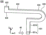
Fig. 17 is a perspective view of a spring terminal 630 according to embodiment 6. In the present embodiment, the structure of the elastic portion 639 is different from that of embodiment 5. At the spring terminal 630, an elastic portion 639 is provided between the 1 st connection portion 631 and the 2 nd connection portion 632. The 2 nd connecting portion 632 has a 1 st end portion 634 connected to the elastic portion 639 and a 2 nd end portion 635 opposite to the 1 st end portion 634. The 2 nd connecting portion 632 has a flat plate shape.
The width of the 2 nd connecting portion 632 as viewed from the direction perpendicular to the upper surface 523 of the housing 520 is smaller than the width in the direction perpendicular to the upper surface 523 of the housing 520. The width of the convex portion 633 provided at the 2 nd end 635 as viewed from the direction perpendicular to the upper surface 523 of the housing 520 is equal to the width of the 2 nd connection portion 632 in that direction.
Fig. 18 is a front view of a spring terminal 630 according to embodiment 6. The elastic portion 639 is bent in a U-shape so as to protrude toward the opposite side of the 2 nd connecting portion 632. The elastic portion 639 generates an elastic force by bending into a U-shape. The spring terminal 630 has elasticity in a direction perpendicular to the upper surface 523 of the housing 520 by the elastic portion 639. The convex portion 633 of the 2 nd end portion 635 is brought into contact with the control substrate 540 by an elastic force generated by the elastic portion 639.
As in embodiment 5, the width of the 2 nd connecting portion 632 when viewed from the direction perpendicular to the upper surface 523 of the housing 520 is smaller than the width in the direction perpendicular to the upper surface 523 of the housing 520. Therefore, the spring terminals 630 easily follow the positional displacement of the control board 540 in the direction along the upper surface 523 of the housing 520. Therefore, the reliability of the contact between the control board 540 and the spring terminal 630 can be improved. In addition, as in embodiment 5, the pitch of the signal terminals of the control board 540 can be narrowed.
Further, the spring terminal 630 according to the present embodiment does not need to be provided with a constriction as in embodiment 5 in order to obtain an elastic force. Therefore, the resistance of the spring terminal 630 can be reduced as compared with embodiment 5. Therefore, the reliability of the electrical connection between the control board 540 and the semiconductor element 16 can be improved.
In addition, the technical features described in the embodiments may be appropriately combined and used.