Detailed Description
Fig. 1 illustrates an embodiment of a multi-aperture imaging apparatus. The multi-aperture imaging apparatus 10 of FIG. 1 includes an image sensor 12 and a plurality 14 of light channels, each of which is illuminated by a respective optic 161、162、163And 164And (4) limiting. Each optical channel 141、142、143、144By means of allocated optical devices 161To 164In the corresponding image sensor area 121、122、123Or 124A channel individual section of the total field of view of the up-projection multi-aperture imaging device 10. For example, image sensor 12 may include an image sensor region 121To 124Of the pixel array of (1). Alternatively, image sensor 12 may include per-image-sensor-area 121To 124A pixel array chip. Further, it would be possible for the image sensor 12 to include cross-image transferSensor region 121To 124An array of pixels extending continuously (i.e. having an image sensor area 12)1To 124A rectangular or differently extending pixel array) in which case, for example, only the image sensor area 12 of this common continuous pixel array of the image sensor 12 is read out1To 124. Different combinations of these alternatives are also possible, such as there being one chip for two or more channels and other chips for additional different channels, etc. In the case of several chips of the image sensor 12, these chips may be mounted, for example, on one or several boards, such as all of them mounted together or in groups, etc.
Optical device 161To 164For example, each consisting of a lens or lens group that may be held by a common holder 18 as shown in fig. 1. Illustratively, the holder 18 is formed of a transparent material and is traversed by the light path of the light channel, but other alternatives for holders exist.
Preferably, the image sensor area 121To 124Are arranged in a common plane, i.e. the image plane of the light tunnel 14. In fig. 1, this plane is exemplarily shown parallel to the plane spanned by the x-axis and the y-axis of the cartesian coordinate system shown in fig. 1 for simplifying the subsequent description and having the reference numeral 20.
For example, in a plane parallel to the image sensor 12 (i.e., parallel to the xy plane), the optics 161To 164Are also arranged adjacent to each other. In the example of fig. 1, the image sensor region 121To 124Relative position in the image sensor plane is additionally with the optics 161To 164And an optical device 161To 164The relative positions along the x-axis and y-axis are coincidentally positioned, i.e., laterally with respect to the image sensor 12, such that the optics 161To 164Relative to the image sensor area 121To 124Is located at the center. This means that: in the example of fig. 1, the optical channel 141To 144Optical axis 22 of1To 224Extending parallel to each other and to the z-axis of a coordinate system 20, an image sensor area 121To 124And an optical device 161To 164Centered with respect to its optical axis. It should be noted that there is also a reference to the image sensor area 121To 124And an optical device 161To 164An alternative to the above-described configuration. For example, the optical axis 221To 224Will also be possible. In addition, it is possible that the multi-aperture imaging apparatus comprises optics 16 that are capable of changing in a lateral direction (i.e. in the x-direction and/or the y-direction)1To 164Relative to the image sensor area 121To 124Such as one or several devices for image stabilization. In this regard, please refer to FIG. 10.
Optical device 161To 164Projecting objects in a scene having an overall or total field of view of multi-aperture imaging device 10 onto assigned image sensor region 121To 124To this end, an optical device 161To 164Are arranged at a respective spacing or a respective distance from the image sensor 12. Although the distance may also be fixed, the multi-aperture imaging apparatus may alternatively have means for changing this image sensor-to-optics distance (such as for manually or automatically changing the focus).
In FIG. 1, a plurality 14 of channels 141To 144Formed as a single row array. In the case of fig. 1, the light channel 141To 144Disposed adjacent to each other along the x-axis. Thus, the x-axis corresponds to the row extension direction of the array 14. Image sensor area 121To 124Also arranged adjacent to each other along the direction. In fig. 1, the number of optical channels is illustratively four, but different numbers greater than or equal to two are also possible. In the case of a linear array of light channels as shown in fig. 1, the dimensional extension of the multi-aperture imaging apparatus 10 (limited towards the bottom by the image sensor 12 and optics 16) is greatest along the row extension direction. As by image sensor 12 and optics 16 along the z-axis (i.e., alongLight tunnel 141To 144Optical axis or optical path) is less than the minimum extension along the x-axis, but due to the light tunnel 141To 144Implemented as a single row array, the minimum extension of the multi-aperture imaging device 10 is therefore greater than the minimum extension of the multi-aperture imaging device in a lateral direction y perpendicular to the row extension direction x. The latter consisting of each individual light channel 141To 144Such as the optical device 161To 164Extending along the x-axis, possibly including the holder 18). In this case, depending on the application, such as the mounting of the multi-aperture imaging device into the housing of a portable device (e.g., a mobile phone, etc.), where the housing is very flat, it may be desirable to align the image sensor 12 with the optics 161To 164So that the field of view of the optical channel without beam deflection actually observes a direction deviating from the actual desired field of view direction of the multi-aperture imaging device 10. For example, it may be desirable to install multi-aperture imaging apparatus 10 such that image sensor 12 and optics 161To 164Aligned perpendicular to the largest or major side of the flat housing, i.e. the image sensor 12 and the optics 161To 164Optical axis 22 therebetween1To 224Parallel to these main sides, while the scene to be captured is in a direction perpendicular thereto, i.e. in front of one main side being e.g. the front side and e.g. comprising a screen, or in front of the other main side being e.g. the back of the housing.
For this reason, the multi-aperture imaging device 10 includes a beam deflecting device that deflects the optical paths or axes 22 of the plurality of optical channels 141To 224Such that the total field of view of the multi-aperture imaging apparatus 10 (as seen from the multi-aperture imaging apparatus 10) is not in the direction of the z-axis but elsewhere. Fig. 1 presents an exemplary case where the total field of view of the multi-aperture imaging device 10 after deflection is substantially along the y-axis (i.e., deflection occurs substantially in the zy-plane).
Before discussing additional functions of the beam deflection device 24, it should be noted that the explanation regarding the single row characteristics of the light channel array 14 should not be taken asBy way of limitation, and examples of the present application also include embodiments in which a plurality of optical channels are configured in a two-dimensional array. For example, from a different perspective than that discussed above, it may be desirable to implement the overall field of view of the multi-aperture imaging apparatus 10 relative to the image sensor 12 and optics 161To 164Combined reorientation of (a). Such an aspect may also focus on additional functions of the beam deflection apparatus 24, for example, as described below.
As described above, in the embodiment of FIG. 1, the optical axis 221To 224Before or without deflection by the beam deflection device 24 or, for example, in the optics 16 as shown in fig. 11To 164Are parallel to each other or only slightly offset therefrom. Optical device 161To 164And an image sensor area 121To 124The corresponding centering of (a) is easy to manufacture and advantageous in minimizing installation space. The parallelism of the light paths of the light channels also has a single channel 141To 14NCovering or projecting onto the respective image sensor area 121To 124The partial fields of view above will completely overlap without any further measures (i.e. beam deflection). In order to cover a larger total field of view by the multi-aperture imaging apparatus 10, an additional function of the beam deflection apparatus 24 of FIG. 1 is to provide an optical path having a divergence such that the channel 141To 14NAre less overlapping with each other.
For example, suppose an optical channel 141To 144Optical axis 22 of the optical path of1To 224Parallel to each other before the beam deflection device 24 or without the beam deflection device 24, or offset from the optical channel 14 relative to the parallel orientation along an orientation averaged across all channels1To 14NIs smaller than one tenth of the smallest aperture angle of the partial field of view. Without any additional measures, the partial fields of view will mostly overlap. Thus, the beam deflection device 24 of fig. 1 is for each light channel 141To 14NComprising a reflective facet 26 specifically assigned to the channel1To 264Each of which isAre optically flat and inclined to each other, i.e. so that the partial fields of view of the light channels overlap less in spatial angle and cover, for example, have a larger size than the light channels 141To 14NOf the individual partial fields of view of the field of view of the field of view of the field of view of the field. In the exemplary case of fig. 1, the reflective facets 261To 264Have, for example, light channels 14 arranged linearly along the x-axis, virtually adjacent to one another1To 14NAccording to a partial field of view 301To 304To cover the effect of the total field of view 28.
If the light channel 14 is considered in the embodiment of fig. 1 in a plane spanned or defined by the averaging direction of the optical axis before the beam deflection and the averaging direction of the optical axis after the beam deflection (i.e. in the xy-plane in the example of fig. 1 on the one hand and in a plane extending perpendicular to the latter plane and parallel to the averaging direction of the optical axis after the beam deflection) in the embodiment of fig. 11To 144Optical axis 22 of1To 224The angular deflection of (a) results in the behavior shown in fig. 2a and 2 b. FIG. 2a shows the beam deflection α in a first planexAnd figure 2b shows the beam deflection in the latter plane, i.e. alphaz. Fig. 2a and 2b show the case of an average beam deflection of the optical axis such that the average direction after beam deflection corresponds to the y-axis. On average, the optical axis of the light channel is deflected by 90 ° around the x-axis in the yz-plane, and on average the optical axis is not tilted out of the yz-plane.
As indicated by the dotted line in fig. 1 with 32, the substantially prism-shaped body may be formed as a beam deflection device, but this will be accompanied by the disadvantages already indicated in the introductory part of the description of the present application: the losses that occur during molding depend on the amount of material to be formed, and therefore molding a body as indicated by 32 would entail increasing production costs or causing the light tunnel 141To 14NThe quality of the optical projection of (2) is low.
For the latter reason, as explained in more detail below, the
beam deflection device 24 of fig. 1 is produced such that the
beam deflection device 24 comprises a
plurality 14 of optical channels in common (i.e., that the optical channels are collectively owned by the device 24)Extending across all optical channels). The
carrier substrate 34 is inclined at a set angle with respect to the image sensor 12
(i.e. the axis around which the average direction of the optical axis of the light channel is deflected, i.e. the x-axis in fig. 1). This setting angle has the following effects: the surface of the
beam deflection device 24 facing the image sensor already effects a "coarse deflection" of the optical path of the light channel.
If it is not
For example, as a
light tunnel 14 around the x-axis
1To 14
4 Optical axis 16 of
1To 16
4The minimum beam deflection (i.e.,
wherein
Equal to the
light channel 14
iIs deflected by
Meaning that no beam deflection occurs), the
carrier substrate 24 may be tilted with respect to the
image sensor 12 such that
Is applicable therein
Greater than 0 DEG and less than 90 DEG,
corresponding to a plane parallel orientation of the
carrier substrate 34 to the
image sensor 12. This will be discussed below with reference to fig. 4 a. It can be seen that in this case, the
reflective facets 26
1To 26
4Not tilted in the yz plane relative to the substrate or only in that directionIs inclined such that the lateral surface of the substrate closer to the image sensor is narrower than the lateral surface directed in the opposite direction. When the equation (i.e.,
) Where applicable, there is at least one facet that is not tilted with respect to the substrate in the yz plane.
May be, for example, a
light tunnel 14 around the x-axis
1To 14
4 Optical axis 16 of
1To 16
4The maximum beam deflection of (a), i.e.,
the
carrier substrate 24 may then also be tilted with respect to the
image sensor 12, for example, such that
The method is applicable. This will be discussed below with reference to fig. 4 b. It can be seen here that in this case the
reflective facets 26
1To 26
4Not tilted in the yz plane with respect to the substrate or tilted only in this direction, so that the lateral surface of the substrate closer to the image sensor is wider than the lateral surface directed in the opposite direction. If the equation (i.e.,
) Where applicable, there is at least one facet that is not tilted with respect to the substrate in the yz plane.
In the described manner, it is possible that the
beam deflection device 24 comprises, in addition to the pure parallelepiped shape, an additional material only on the side facing the image sensor 12 (in addition to the pure parallelepiped shape) in order to form the
reflective facets 26
1To 26
4Of the first and second arms. However, these angles of inclination to total deflection
Much smallerSince these tilt angles only perform a residual deflection of the optical path. For tilt angles in the yz plane
(i.e., residual deflection about the x-axis),
the method is applicable. The tilt angle in the yz plane corresponds to half of the individual deflection of the finer channels. In other transverse directions involving deflection of light beams out of the YZ plane, deflection angles
Is small anyway, and therefore the angle of inclination of the facets along the x-axis out of the substrate plane
And in any case small.
For the deflection angles of the optical paths of each optical channel deflected by the
beam deflection device 24, this means that these deflection angles are each based on a set angle
And the corresponding inclination of the reflective facets assigned to the light channels with respect to the
carrier substrate 34 itself. The
facet 26 can be described by the inclination angle in the yz plane and the inclination angle in the plane perpendicular thereto with respect to the normal of the
carrier substrate 3 as described above
1To 26
4The mentioned faces of (a) are individually sloped. When it is applicable, it is preferable to set the angle for each channel
Greater than the inclination, i.e., for all channels,
more preferably, for
Or even for
The inequality has been satisfied. In other words, it is preferable that the setting angle is compared to the
facet 26
1To 26
NIs large so that the additional material with respect to the pure parallelepiped shape of the
beam deflection device 24 is low.
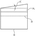
May, for example, be between 30 ° and 60 ° (including 30 ° and 60 °).
Fig. 3a to 3d show side views of a beam deflection device according to an embodiment for an example of 4 light channels configured linearly or on one side as exemplarily shown in fig. 1. The
beam deflection device 24 of fig. 3a to 3d may be used as the beam deflection device of fig. 1, wherein the partial field of view will not cover the total field of view in the
clockwise direction 3, 4, 2, 1 as shown in fig. 1, but in the clockwise direction according to the
sequence 4, 2, 1, 3. The
facets 26 are shown in fig. 3a to 3d
1To 26
4The angle of inclination of (a). The tilt angles of the facets are distinguished from each other or assigned to the respective channels by
subscript indices 1 to 4. Here, the first and second liquid crystal display panels are,
and
are all 0. The rear side of the carrier substrate (i.e. with the
facets 26 provided therewith)
1To 26
4The opposite side of the surface) is indicated by 36 in fig. 3a to 3 d. The material forming the parallelepiped-shaped portion of the
carrier substrate 34 is below the dotted
lines 38. It can be seen that the additional material to be added to the material has a very small volume, making moulding easier.
The production of the beam deflection device 24 of fig. 3a to 3d may for example be performed in that additional material is moulded onto the carrier substrate 34 by a moulding tool. Here, the carrier substrate 34 may be glass, while the molded additional material thereon is a polymer. Another option would be to integrally form the beam deflecting device 24 of fig. 3 a-3 d by injection molding or the like.
In the above statement, it has been described that: as indicated in FIG. 4a, the
channel 14
i Facet 26 of
iMay be tilted around the x-axis or in the same direction in the yz-plane, i.e. the setting angle of the
carrier substrate 34 of the tilting
beam deflection device 24 with respect to the
image sensor 12
So that it is suitable for all
facets 26 of all channels having a thickness of the
beam deflection device 24 on the
side 40 farther away from the
image sensor 12 that is greater than the thickness of the
beam deflection device 24 on the
side 42 closer to the image sensor
i. However, there are alternatives to the situation shown in fig. 4b and 4 c. According to fig. 4b, the situation stated above is reversed. This means that
facet 26 in the yz plane
iAngle of inclination (i.e., inclination)
) So that it is suitable for all
facets 26 of the
beam deflection device 24 having an image
sensor facing side 42
iWith
side 42 being thicker than on
side 40 facing away from the image sensor. Thus, fig. 4b applies with reference to fig. 2a and 2 b:
according to fig. 4c, two situations are possible; i.e.
facet 26
iTilted according to fig. 4a, and
facets 26
jTilted according to fig. 4 b. Therefore, the temperature of the molten metal is controlled,
the method is applicable.
Thus, the embodiment of FIG. 1 with the deflection device of FIG. 3 represents a multi-aperture imaging device in which each channel is in the image sensor region 12iDefines a projection thereon and includes assigned imaging optics 16iAnd by the allocated segments or facets 16 of the beam deflection device 14iAnd (4) deflecting. Facet 26iRepresentation oriented graphLike part of the surface or side of the beam deflection device 24 of the sensor 12. The facets may be produced by molding a polymer, such as a UV curable polymer, on a common planar substrate 34, such as glass, polymer, metal, silicon, or other suitable material. Formed of a planar substrate 34 and prisms molded thereon (i.e., each channel 14)iA prism) can be associated with the imaging channel 14, wherein the body forms the deflection device 24iOptical axis 22 ofiAligned such that the surface normal of the substrate 34 (i.e., the normal on the parallelepiped-shaped portion of the beam deflecting device 24) is aligned with the optical axis 22iAn angle of > 0 and < 90 ° is formed, which is preferably about 45 ° or between 30 ° and 60 ° (including 30 ° and 60 °).
According to an embodiment, a plurality of deflection devices 24 are produced simultaneously on the substrate by means of a replication process. The examples will be as follows. In order to provide the facet 26 with reflective capabilityiReflective material or orientable facet 26 may be moldediProvides a mirror image. The mirror may include both a metal layer and a dielectric layer.
Furthermore, in other words, the deflecting device according to fig. 3 can be produced in a versatile manner. Here, the deflection device as indicated in fig. 5a may be produced by molding, for example, a polymer on a planar substrate, or the production may be performed by casting or embossing glass or a polymer, so that a single component entity as indicated in fig. 5b is produced. The individual deflection devices can then be singulated by sawing, laser, sanding or water jet cutting. It is clear that the separation can be performed by means of saw cuts 43 perpendicular to the carrier substrate 34 or perpendicular to the rear side 38 of the carrier substrate. Advantageously, however, the separation can also be carried out such that the cutting surface resulting from the singulation cuts forms an angle ≠ 0 with respect to the area normal of the carrier substrate 34. The vertical cuts are shown in fig. 6a for the case of molding a polymer on a carrier substrate and in fig. 6b for the case of embossing a material with subsequent vertical cuts, and fig. 7 shows a singulation along an inclined cutting surface 43 (i.e. along a cutting surface at an angle to the area normal of the carrier substrate), exemplarily for the case of molding a polymer on a planar carrier substrate.
FIG. 8 showsThe reason for this situation is: the cut angles of the singulation cut planes arranged between adjacent deflection devices running parallel to the row extension direction may be selected such that, when these deflection devices are mounted into the
multi-aperture imaging device 10, these cut surfaces are parallel or nearly parallel to the
light tunnel 14 before or without beam deflection
iOptical axis 22 of
iBut extended so as to yield, in general, a minimum mounting height for the overall system of the
multi-aperture imaging apparatus 10. Fig. 8 shows the minimum mounting height resulting therefrom, as explained for the case of fig. 4b, in which, for each channel i, the facet in the yz plane (i.e. in the plane in which the setting angle is at a maximum) is inclined such that the
side 40 of the
carrier substrate 34 furthest away from the
image sensor 12, which runs perpendicular to the above-mentioned plane (i.e. parallel to the row extension direction of the image sensor 12), is used for forming the
facet 26
iWithout or with less enlargement in the thickness direction of the
carrier substrate 34 relative to the parallelepiped shape of the
carrier substrate 34. As shown in FIG. 8, these
sides 40 and 42 are parallel to the optical path or axis 22
iBut extends on the image sensor side. Advantageously, in the configuration of fig. 4b, the singulation plane, indicated by the
lines 43 in fig. 6a, 6b and 7, does not intersect the additional material forming the facets. In the configuration of fig. 4a, this will not be the case for all facets, and in the configuration of fig. 4c, will not be the case for those facets corresponding to the configuration of fig. 4 a. However, as shown by a comparison between fig. 4b and fig. 8, the mounting height in the y-direction is not reduced in the case of fig. 8 relative to the case of fig. 4 b. For the angle γ between the
side 40 and the
rear side 36 in the yz plane, the following applies:
fig. 9 shows exemplarily for the case of fig. 4 a: symmetrical to the rear side 36, the beam deflection device may comprise, in addition to the substrate 34, an identically formed substrate 34'. By passingThe pivotal suspension of the beam deflection device 24 about an axis 48 running along the row extension direction or along the x-axis, the beam deflection device 24 being changeable from a position I with a setting angle as described above to a position II with a setting angle corresponding to a relative inclination with respect to the image sensor 12 and thus having the following effect: in position I, facet 26iThe beam deflection mentioned above is achieved, whereas in position II the facet 26i' implementation is as shown by 22 in FIG. 9iOr 22iThe beams in substantially opposite directions are deflected as indicated by'. It is obviously also possible to apply this reversibility by rotation about the axis 48 also in the configuration according to fig. 4b or 4 c. For production, for example, the back sides 36 of the two substrates 34 and 34' may be connected to each other, such as by adhesive bonding or another bonding process.
In the above, it has been mentioned that the optical path or the optical axis may deviate from being parallel before the beam deflection or without the beam deflection. This will be described below by the fact that the channels may be provided with some pre-divergence. At the optical axis 221To 224With such pre-divergence it would be possible, for example, that not all facets are of different inclination, but some channel groups have, for example, facets of the same inclination. The facets of the same inclination can then be integrally formed or merge continuously with one another, in fact as one facet assigned to the group of channels adjacent in the row extension direction. The divergence of the optical axes of the channels may then result from the divergence of these optical axes as obtained by the lateral offset between the optics of the channels and the optical center of the image sensor area. The pre-divergence may be limited to one plane, for example. Before or without beam deflection, the optical axis may, for example, extend in a common plane, but diverge in a common plane, and the facets only achieve an additional divergence in another transverse plane, i.e. they are all parallel to the row extension direction (for all i, β)i z0) and are inclined with respect to one another, the other transverse plane being only different from the above-mentioned common plane of the optical axis, wherein several facets may again have the same inclination, or may be inclinedAre assigned together to groups of channels of the optical axis which differ, for example, in pairs in the common plane of the optical axis mentioned above before or without beam deflection.
The pre-divergence that may be present as mentioned above may be obtained, for example, by arranging the optical centers of the optics on a straight line along the row extension direction, while the centers of the image sensor areas are configured in such a way that the projections of the optical centers deviate along the normal of the plane of the image sensor areas at the points of the straight line in the image sensor plane, such as at points deviating from the points on the straight line as mentioned above in the image sensor plane along the row extension direction in a channel-by-channel manner and/or along a direction perpendicular to both the row extension direction and the image sensor normal. Alternatively, a pre-divergence may be obtained in that the center of the image sensor is on a straight line along the row extension direction, while the center of the optics projected from the optical center of the image sensor is configured in such a way that it deviates along the normal of the plane of the optical center of the optics on a point of the straight line in the optical center plane (such as at a point deviating from the point on the above mentioned straight line in the optical center plane along the row extension direction in a channel-by-channel single manner and/or along a direction perpendicular to both the row extension direction and the normal of the optical center plane). Preferably, the above-mentioned individual deviations of the channels from the respective projections extend only in the row extension direction (i.e. the optical axes in the common plane are provided with a pre-divergence). Then, both the optical center and the image sensor area center are on a line parallel to the row extension direction, but with different intermediate distances. In contrast, a lateral offset between the lens and the image sensor in a perpendicular direction lateral to the row extension direction will result in an enlargement of the mounting height. Merely an offset in the plane in the direction of the row extension does not change the mounting height, but possibly fewer facets will be produced and/or the facets will only have an inclination in the angular orientation of the simplified structure. This is illustrated in fig. 13a and 13b, where on the one hand adjacent to the channel 141And 142And on the other hand adjacent to the channel 143And 144Having extension in a common plane and phaseFor optical axes 14 that are skewed with respect to each other (i.e. have a pre-divergence)1And 142Or 143And 144. Facet 261And 262May be formed of one facet and facet 263And 264May be formed by another facet as indicated by the dotted line between the respective facet pair, and only two facets are tilted in only one direction and both are parallel to the row extension direction, i.e. (for all i, β)i z0 and betai xNot equal to 0, and β1 x=β2 xAnd beta is3 x=β4 x)。
In addition, it is contemplated that some light channels are assigned to the same partial field of view, such as for super-resolution purposes or for increasing the resolution at which the respective partial field of view is sampled by the channels. The light channels within the group will then be spread in parallel before the beam is deflected and will be deflected by the facets onto part of the field of view. Advantageously, the image of the pixels of the image sensors of one channel of a group will be located in an intermediate position between the images of the pixels of the image sensors of the other channel of the group.
An embodiment is also possible in which the group of immediately adjacent channels in the row extension direction completely covers the total field of view with its partial field of view and the other group of immediately adjacent channels in its part also completely covers the total field of view, for example not for super-resolution purposes but only for stereo viewing purposes.
Fig. 10 shows that the multi-aperture imaging apparatus 10 of fig. 1 may additionally comprise means 50 for effecting rotation of the beam deflecting device 24 about an axis parallel to the row extension direction or x-axis. The axis of rotation being, for example, at the optical axis 221To 224In-plane or with a smaller deviation than the optical device 161To 164One quarter of the diameter of (a). Alternatively, it would also be possible that the rotation axes are further spaced apart, such as less than one optic diameter or less than four optic diameters. This means 50 may, for example, be part of the image stabilization control of the device 10 by adaptively changing the setting angle and/or for referencing the map9 to compensate for the blur about the x-axis by moving the beam deflection device 24 between the position I and the position II mentioned above.
Additionally, the multi-aperture imaging apparatus 10 of fig. 10 may additionally or alternatively include implementing optics 16iMeans 52 for translational movement along the x-axis. The device 52 may also be part of image stabilization and may achieve blur, for example, in a direction perpendicular to the above-mentioned blur compensation via the device 50.
Additionally or alternatively, the apparatus 10 may further comprise adjusting along the optical axis 22 for focus adjustmentiAnd the image sensor 12 and the optics 16. This means 54 may be controlled by an autofocus control or also manually by the user of the device in which the device 10 is installed.
Thus, the device 52 acts as a suspension for the optics, and preferably, as indicated in fig. 4, the device 52 is arranged laterally adjacent thereto along the row extension direction, so as not to increase the mounting height. It also applies to the devices 50 and 54, the devices 50 and 54 preferably being arranged in the plane of the light path so as not to increase the installation height.
It should be noted that optic 161To 164May be held not only in each other (such as via the transparent substrates already mentioned), but also in a constant relative position with respect to the beam deflection device (such as via a suitable frame which preferably does not increase the mounting height and therefore preferably extends in the plane of the components 12, 14 and 24 or in the plane of the light path). The consistency of the relative positions may be limited to the distance along the optical axis between the optics and the beam deflection device, such that the means 54 moves the optics 16 (for example) along the optical axis in a translational manner1To 164And a beam deflecting device. The optics-to-beam deflection device distance can be set to a minimum distance such that the optical path of the channel is not laterally limited by the segments of the beam deflection device 24, which can reduce the mounting height, since the segments 26, if not soiWill have to be dimensioned for the maximum optics-to-beam deflection device distance with respect to the lateral extension so as not to restrict the optical path. In addition, the above-mentioned phases of the frameThe consistency of the position may hold the optics and the beam deflection apparatus to each other along the x-axis in a rigid manner such that the device 52 will move the optics 16 along the row extension direction in a translational manner1To 164And a beam deflecting device.
The above-described beam deflection device 24 for deflecting the optical path of the optical channel achieves image or total field of view stabilization in two dimensions together with the actuator 50 for generating a rotational movement of the beam deflection device 24 for the optical image stabilization control of the multi-aperture imaging device, i.e. along a first image axis running substantially parallel to the beam deflection device by a translational movement of the substrate 18 and along a second image axis running substantially parallel to the optical axis by generating a rotational movement of the beam deflection device 24 before beam deflection or in the absence of beam deflection, or taking into account a deflected optical axis perpendicular to the optical axis and the line extension direction. In addition, the described configuration can enable, for example, translational movement of the array 14 perpendicular to the row extension direction and beam deflection apparatus fixed in the frame set forth above, which can be used to enable focus adjustment and thus for implementing autofocus functions, by the described actuator 54.
For completeness, it is noted with respect to the above statement that the device captures one image of a scene per channel as captured via the image sensor area, which has been projected onto the image sensor area by the channel, and that the device may optionally have a processor that combines or merges the images into an overall image corresponding to the scene in the overall field of view and/or provides additional data such as 3D image data and depth information for generating a depth map and for software implementation such as refocusing (determining the image sharpness area after actual capture), all in focus images, a virtual green screen (separation of foreground from background), etc. The latter tasks may also be performed by the processor or also externally. However, the processor may also represent a component external to the multi-aperture device.
With respect to the above statements, it should still be noted that the facets 26iCan be mirrored. Alternatively, in addition toIt is also possible to form additional material beyond the parallelepiped-shaped part of the carrier substrate of the mirror image material, so that a separate mirror image can be omitted.
Fig. 11 shows that the above-described alternative embodiment of the device 10 can be incorporated, for example, in a flat housing of a portable device 200, such as a mobile phone or a media player, etc., wherein then, for example, the plane of the image sensor 12 or the image sensor area and the lens plane of the optics of the channel 14 are aligned perpendicular to the flat extension direction of the flat housing or parallel to the thickness direction. In this way, for example, the beam deflection apparatus 24 will have the effect that the total field of view of the multi-aperture imaging apparatus 10 is in front of the front side 202 of a flat housing that also includes, for example, a monitor. Alternatively, deflection is also possible so that the field of view is located in front of the back side of the flat housing opposite the front side 202. The housing may include a transparent window in the pass-through side 202 to allow the light path of the light channel 14 to pass through. In addition, switchable diaphragms (mechanically moved, electrochromic) may be attached in order to influence the light entry through the opening of the window on the front side and/or the back side. The housing of the device 200 or the device itself may be flat because: due to the shown position of the device 10 in the housing, the mounting height of the device 10 (which is parallel to the thickness of the housing) can be kept low. Switchability may also be provided in that the window is provided on the side opposite to the side 202 and the beam deflection device is moved between the two positions, for example by configuring the side 202 as a mirror mirrored on the front and on the back (and with one position rotated to the other) as shown in fig. 9, or as a facet mirror with a set of facets for one position and a different set of facets for the other position (with the sets of facets being adjacent to each other in the direction of row extension and switching between the positions being performed by moving the beam deflection device back and forth in a translational manner along the direction of row extension). It is also possible to mount the device 10 into another possible non-portable device, such as a car. Fig. 12 shows that several modules 10, of which the partial fields of view of the channels completely and optionally even superpositionally cover the same field of view, can be mounted in the device 200, for example, at a base distance B from each other along the same row extension direction for both modules, such as for stereoscopic viewing purposes. More than two modules would also be possible. The row extension directions of the modules 10 may also be non-collinear, but only parallel to each other. However, it should still be mentioned that, as stated above, the apparatus 10 or module may be provided with channels such that the channels completely cover the same total field of view in groups.
Thus, the above embodiments may be implemented in the form of a multi-aperture imaging device having a single row channel arrangement, where each channel transmits a partial field of view of the total field of view and the partial fields of view partially overlap. The structure of several of such multi-aperture imaging devices with stereoscopic, triplex, quadruplex, etc. structures for 3D image capture is possible. Here, the plurality of modules may be configured as a continuous line. Successive lines may use the same actuator and common beam deflection assembly. One or several magnifying substrates that may be present in the optical path may extend across the entire line that may form a three-dimensional, four-dimensional structure. A method for super resolution may be used in which several channels project the same partial image area. The optical axis may diverge even without any beam deflection device, so that fewer facets are required on the beam deflection unit. Advantageously, the facets then have only angular components. The image sensor may be a one-piece unit and may have only one continuous matrix of pixels or several discontinuous matrices of pixels. The image sensor may be combined by several partial sensors, for example arranged adjacent to each other on a printed circuit board. The autofocus drive may be configured such that the beam deflection assembly moves synchronously with the optics or is stationary.