Detailed Description
The following disclosure provides many different embodiments, or examples, for implementing different features of the invention. Specific examples of components and arrangements are described below to simplify the present disclosure. These are, of course, merely examples and are not intended to be limiting. For example, the description that a first feature is formed over or on a second feature encompasses embodiments in which the first and second features are in direct contact, as well as embodiments in which other features are formed between the first and second features such that the first and second features are not in direct contact. The dimensions of many of the features may be drawn on different scales to simplify and clarify the same. In addition, the present disclosure may repeat reference numerals and/or letters in the various examples. This repetition is for the purpose of simplicity and clarity and does not in itself dictate a relationship between the various embodiments and/or configurations discussed.
Furthermore, the spatially relative terms, such as "below", "below" … "," below "," above … "," above ", and the like, are used for ease of describing the relationship of the elements or features to one another. Spatially relative terms may encompass different orientations of the elements in use or operation in addition to the orientation depicted in the figures. The device may be otherwise oriented (rotated 90 degrees or at other orientations) and the spatially relative descriptors used herein interpreted accordingly.
It should be noted that references in the specification to "one embodiment," "an example" or the like indicate that the embodiment described may include a particular feature, structure, or characteristic. Moreover, the above-described terms are not necessarily intended to represent the same embodiment. Furthermore, when a particular feature, structure, or characteristic is described in connection with an embodiment, it is submitted that it is within the knowledge of one skilled in the art to affect such feature, structure, or characteristic in connection with other embodiments whether or not explicitly described.
It is to be understood that the phraseology or terminology herein is for the purpose of description and not of limitation, such that the terminology or phraseology of the present specification is to be interpreted by the skilled artisan in light of the teachings herein.
The term "selectivity" as used herein refers to the ratio of etch rates between two materials under the same etch conditions.
The term "about" as used herein, unless otherwise specified, means that the magnitude of the change in the numerical value of the stated quantity is within 10% of the numerical value.
The term "substrate" as used herein is intended to describe a material onto which a subsequent layer of material is applied. The substrate itself may be patterned. The material added on top of the substrate may be patterned or may remain unpatterned. Further, the substrate may be any of a range of semiconductor materials, such as silicon, germanium, gallium arsenide, indium phosphide, and the like. In addition, the substrate may be made of a non-conductive material, such as glass or sapphire wafers.
The term "high k" as used herein means a high dielectric coefficient. In the field of semiconductor devices and processes, high k represents a dielectric constant greater than that of silicon dioxide (i.e., greater than 3.9).
The term "low k" as used herein means a low dielectric coefficient. In the field of semiconductor devices and processes, low k represents a dielectric constant less than that of silicon dioxide (i.e., less than 3.9).
Any structure, layer and/or region defined by the term "p-type" as used herein is doped with a p-type dopant, such as boron.
Any structure, layer and/or region defined by the term "n-type" as used herein is doped with an n-type dopant, such as phosphorus.
SUMMARY
The present disclosure provides exemplary methods of fabricating n-type finFETs (NFETs) and p-type finFETs (PFETs) of semiconductor devices using a dual epitaxial growth process. These methods provide for high selectivity and conformal growth of n-type and p-type epitaxial regions on fin structures of n-type and p-type finfets, respectively, as compared to other methods of forming epitaxial regions on fin structures of n-type and p-type finfets. The highly selective growth of the epitaxial region achieves a substantial reduction or minimization of the disruption of the structural and functional integrity of the n-type and p-type finfets as compared to n-type and p-type finfets of other semiconductor devices.
Embodiments of devices with n-type and p-type finfet transistors
Fig. 1A and 1B are isometric views of the device 100 after a gate replacement process according to some embodiments. Fig. 1B is a 180 degree rotated (i.e., along the Z-axis) view of the device 100 according to fig. 1A. Fig. 1C-1E are cross-sectional views of a semiconductor device along lines a-a, B-B, and C-C of fig. 1A, respectively, according to some embodiments. The apparatus 100 may be embodied in a microprocessor, memory device, or other Integrated Circuit (IC). It should be understood by those skilled in the art that the views of the apparatus 100 in fig. 1A-1E are presented for illustrative purposes and are not drawn to scale.
The apparatus 100 discussed in this section is shown in FIGS. 1A-1E. The device 100 may be formed on a substrate 102 and may include p-type fin field effect transistors (PFETs)104.1 through 104.4 and n-type fin field effect transistors (NFETs)106.1 through 106.4. The device 100 may further include a Shallow Trench Isolation (STI) region 108, gate structures 110.1 through 110.6, and spacers 112, wherein the spacers 112 are disposed on opposite sidewalls of each of the gate structures 110.1 through 110.6.
The substrate 102 may be a physical material on which the p-type finfet 104.1-104.4 and the n-type finfet 106.1-106.4 are formed. The substrate 102 may be a semiconductor material such as, but not limited to, silicon. In some embodiments, the substrate 102 comprises a crystalline silicon substrate (e.g., a wafer). In some embodiments, the substrate 102 comprises (i) an elemental semiconductor, such as germanium; (ii) a compound semiconductor comprising silicon carbide, gallium arsenide, gallium phosphide, indium arsenide, and/or indium antimonide; (iii) an alloy semiconductor comprising silicon germanium carbide, silicon germanium, gallium arsenic phosphide, indium gallium arsenide, indium gallium phosphide arsenide, aluminum indium arsenide and/or aluminum gallium arsenide; or (iv) combinations of the foregoing. Furthermore, the substrate 102 may be doped according to design requirements (i.e., p-type substrate or n-type substrate). In some embodiments, the substrate 102 may be a p-type dopant (e.g., boron, indium, aluminum, or gallium) or an n-type dopant (e.g., phosphorus or arsenic).
The sti regions 108 may provide electrical isolation of the p-type finfet 104.1 to p-type finfet 104.4 and the n-type finfet 106.1 to n-type finfet 106.4 from each other and from adjacent active and passive devices (not shown) that are bonded to the substrate 102 or deposited on the substrate 102. The shallow trench isolation region 108 may be made of a dielectric material. In some embodiments, the shallow trench isolation region 108 may comprise silicon oxide, silicon nitride, silicon oxynitride, fluorine-doped silicate glass (FSG), low-k dielectric material, and/or other suitable insulating materials. In some embodiments, the shallow trench isolation region 108 may comprise a multi-layer structure.
In some embodiments, p-type finfet 104.1-104.4 may include fin structures 114.1-114.4 and p-type epi regions 116.1-116.4, respectively. In some embodiments, n-type finfet 106.1-106.4 may include fin structures 118.1-118.4 and n-type epi regions 120.1-120.4, respectively.
Fin structures 114.1, 114.2, 118.1, and 118.2 may pass through gate structures 110.1, 110.2, and 110.3 along the Y-axis. Fin structures 114.3, 114.4, 118.3, and 118.4 may also pass through gate structures 110.4, 110.5, and 110.6 along the Y-axis. The portions of fin structure 114.1, fin structure 114.2, fin structure 118.1, and fin structure 118.2 that extend below the shallow trench isolation region 108 may be surrounded by gate structures 110.1-110.3, respectively. Similarly, the portions of fin structure 114.3, fin structure 114.4, fin structure 118.3, and fin structure 118.4 that extend below the shallow trench isolation region 108 may be surrounded by gate structures 110.4-110.6, respectively.
In some embodiments, fin structures 114.1-114.4 and fin structures 118.1-118.4 may comprise similar materials as substrate 102. In some embodiments, fin structures 114.1-114.4 and fin structures 118.1-118.4 may be formed from photolithographic patterning and etching of substrate 102. According to some embodiments, the portion of each fin structure 114.1-114.4 and fin structure 118.1-118.4 in the shallow trench isolation region 108 may have a width W1 (as shown in fig. 1E) ranging from about 5nm to about 10 nm. The portion of each of fin structures 114.1-114.4 and 118.1-118.4 extending above shallow trench isolation region 108 may have a width W2 (shown in figure 1E) ranging from about 3nm to about 6 nm. Based on the disclosure herein, one of ordinary skill in the art will appreciate that other widths and materials of fin structures 114.1 through 114.4 and fin structures 118.1 through 118.4 are within the scope and spirit of the present disclosure.
In some embodiments, as illustrated in fig. 1A-1D, p-type epitaxial regions 116.1-116.4 may be grown on portions of fin structures 114.1-114.4, respectively, and extend below the sti region 108 and not below the gate structures 110.1-110.6. Similarly, in some embodiments, fig. 1A-1D illustrate that n-type epitaxial regions 120.1-120.4 may be grown on portions of fin structures 118.1-118.4, respectively, and extend below the sti regions 108 and not below the gate structures 110.1-110.6.
The epitaxial regions 116.1 to 116.4 and 120.1 to 120.3 may comprise epitaxially grown semiconductor material. In some embodiments, the epitaxially grown semiconductor material is the same material as the substrate 102. In some embodiments, the epitaxially grown semiconductor material is a different material than the substrate 102. The epitaxially grown semiconductor material may comprise: (i) semiconductor materials such as germanium or silicon; (ii) a compound semiconductor material comprising gallium arsenide and/or aluminum gallium arsenide; or (iii) an alloy semiconductor comprising silicon germanium and/or gallium arsenic phosphide. In some embodiments, each of the epitaxial regions 116.1-116.4 and 120.1-120.3 may have a thickness T1 (e.g., as shown in fig. 1E) surrounding portions of the fin structure above the shallow trench isolation 108, wherein the thickness T1 is in a range of about 5nm to about 15 nm.
In some embodiments, the epitaxial regions 116.1 to 116.4 and the epitaxial regions 120.1 to 120.3 may be deposited by (i) Chemical Vapor Deposition (CVD), such as Low Pressure CVD (LPCVD), Atomic Layer CVD (ALCVD), Ultra High Vacuum CVD (UHVCVD), Reduced Pressure CVD (RPCVD), or any suitable CVD; (ii) a Molecular Beam Epitaxy (MBE) process; (iii) any suitable epitaxial process; or (iv) combinations of the foregoing. In some embodiments, the epitaxial region 116.1 to the epitaxial region 116.4 and the epitaxial region 120.1 to the epitaxial region 120.3 may be grown by an epitaxial deposition/partial etch process, wherein the epitaxial deposition/partial etch process is repeated at least once. The repeated epitaxial deposition/partial etching process is also referred to as a "cyclic deposition-etch (CDE) process". In some embodiments, growing the epitaxial regions 116.1 to 116.4 and 120.1 to 120.3 is performed by Selective Epitaxial Growth (SEG), wherein an etching gas is added to promote selective growth of semiconductor material on exposed surfaces of the fin structure, but not on the insulating material, such as the dielectric material of the shallow trench isolation region 108.
The p-type epitaxial regions 116.1-116.4 may comprise silicon germanium and may be doped in situ with a p-type dopant, such as boron, indium or gallium, during the epitaxial growth process. For p-type in situ doping, the p-type dopant precursor may be, for example, but not limited to, diborane (B)2H6) Boron trifluoride (BF)3) And/or other p-type dopants may be usedAnd (5) expelling the substance. The n-type epitaxial regions 120.1-120.3 may comprise silicon and may be in-situ doped with an n-type dopant, such as phosphorus or arsenic, during the epitaxial growth process. For n-type in situ doping, the n-type dopant precursor may be, for example, but not limited to, arsine (AsH)3) Phosphine (PH)3) And/or other n-type dopant precursors may be used.
In some embodiments, each of the p-type epitaxial regions 116.1-116.4 may have a sub-region, wherein the sub-regions may comprise silicon germanium and differ from each other according to, for example, doping concentration, epitaxial growth process conditions, and/or relative concentration of germanium with respect to silicon.
For example, as shown in fig. 1E, the epitaxial region 116.1 may have a p-type sub-region 126, a p-type sub-region 128, and a p-type sub-region 130, wherein the p-type sub-region 126, the p-type sub-region 128, and the p-type sub-region 130 are epitaxially grown on the fin structure 114.1, the p-type sub-region 126, and the p-type sub-region 128, respectively. In some embodiments, the p-type sub-region 126, the p-type sub-region 128 and the p-type sub-region 130 may have a thickness 126t, a thickness 128t, a thickness 130t in the range of about 0.5nm to about 5nm, about 2nm to about 5nm and about 0.5nm to about 5nm, respectively. In some embodiments, the atomic percent of germanium in sub-region 126 is less than the atomic percent of germanium in sub-regions 128 and 130. In some embodiments, the atomic percent of germanium in sub-region 126 is equal to or nearly equal to the atomic percent of germanium in sub-region 130, but less than the atomic percent of germanium in sub-region 128. In some embodiments, the sub-region 126 comprises germanium in a range from about 15 atomic percent to about 35 atomic percent, the sub-region 128 comprises germanium in a range from about 40 atomic percent to about 70 atomic percent, and the sub-region 130 comprises germanium in a range from about 25 atomic percent to about 50 atomic percent, with the remainder of the atomic percent being silicon in the sub-region 126, the sub-region 128, and the sub-region 130.
The sub-regions 126, 128, and 130 may be epitaxially grown at a pressure of about 10Torr to about 300Torr and a temperature of about 500 ℃ to about 700 ℃ using a reactive gas, such as hydrogen chloride, as an etchant, germane (GeH)4) As precursor of germanium, silicon dichlorideAlkanes (DCS) and/or Silanes (SiH)4) As a precursor for silicon, diborane as a precursor for boron, hydrogen and/or nitrogen. In order to achieve different germanium concentrations in sub-region 126, sub-region 128, and sub-region 130, the flow rate ratio of the germanium to silicon precursor may be varied during the respective growth processes, according to some embodiments. For example, the flow rate ratio of the germanium to silicon precursor used in the epitaxial growth of sub-region 128 may range from about 9 to about 25, while the flow rate ratio of the germanium to silicon precursor used in the epitaxial growth of sub-region 130 may be less than 6.
According to some embodiments, sub-region 126, sub-region 128, and sub-region 130 may vary the p-type dopant concentration from one another. For example, the sub-region 126 may be undoped or may have a doping concentration that is lower than the doping concentrations of the sub-regions 128 and 130. In some embodiments, the sub-region 126 may have a thickness of less than about 8 x 10²⁰Atom/cm3While sub-region 128 may have a doping concentration in the range of about 1 x 10²⁰Atom/cm3To about 3X 10²¹Atom/cm3And the sub-region 130 may have a doping concentration in the range of about 1 x 10²⁰Atom/cm3To about 3X 10²²Atom/cm3The doping concentration of (c). The epitaxial regions 116.2-116.4 may have sub-regions (not shown) similar to the sub-regions 126, 128 and 130.
As illustrated in fig. 1E, the epitaxial region 120.1 may have an n-type sub-region 132, an n-type sub-region 134, and an n-type sub-region 136, wherein the n-type sub-region 132, the n-type sub-region 134, and the n-type sub-region 136 are epitaxially grown on the fin structure 118.1, the sub-region 132, and the sub-region 134, respectively. The thickness, relative concentration of germanium with respect to silicon, dopant concentration and/or epitaxial growth process conditions of sub-region 132, sub-region 134 and sub-region 136 are similar to sub-region 126, sub-region 128 and sub-region 130, respectively, except for the type of dopant. The epitaxial regions 120.2-120.4 may have sub-regions (not shown) similar to the sub-regions 132, 134 and 136.
As disclosed herein, one of ordinary skill in the art will appreciate that other materials, thicknesses, germanium concentrations, and dopant concentrations for sub-regions 126, 128, 130, 132, 134, and 136 are within the scope and spirit of the present disclosure.
Fin structures 114.1-114.4 and fin structures 118.1-118.4 are current carrying structures for p-type finfet 104.1-104.4 and n-type finfet 106.1-106.4, respectively. The epi regions 116.1-116.4 along the portions of the fin structures 114.1-114.4 covered by the epi regions 116.1-116.4, respectively, are configured to serve as source/drain (S/D) regions of the p-type finfets 104.1-104.4, respectively. Similarly, epi regions 120.1-120.4 along the portions of fin structures 118.1-118.4 covered by epi regions 120.1-120.4, respectively, are configured to serve as source/drain (S/D) regions of n-type finfet 106.1-106.4, respectively. The channel regions of the p-type and n-type finfets are formed in portions of the fin structure below the gate structure. For example, as shown in fig. 1C, the channel region 138 of the p-type finfet 104.1 is formed in the portion of the fin structure 114.1 from the gate structure 110.1 to below the gate structure 110.3. Such as the channel region 140 of the exemplary n-type finfet 106.1 shown in fig. 1D. Channel region 140 is formed in gate structure 110.1 through the portion of fin structure 118.1 of gate structure 110.3.
The gate structure 110.1 is discussed further below with reference to fig. 1C and 1D. However, since gate structures 110.1-110.6 have similar structures, compositions, and functions to each other, it is to be understood that the discussion of gate structure 110.1 is applicable to gate structures 110.2-110.6 unless otherwise noted.
As shown in fig. 1C and 1D, the gate structure 110.1 may include a dielectric layer 122 and a gate electrode 124. For simplicity, the dielectric layer 122 and the gate electrode 124 are not shown in fig. 1A and 1B. In some embodiments, the dielectric layer 122 is adjacent to and in contact with the gate electrode 124. In some embodiments, the thickness of the dielectric layer 122 ranges from about 1nm to about 5 nm. In some embodiments, the gate structure 110.1 may further include a capping layer, an etch stop layer, and/or other suitable materials. The gate structure 110.1 may be formed by a gate replacement process.
The dielectric layer 122 may comprise silicon oxide and may be formed by chemical vapor deposition, atomic layer deposition, physical vapor deposition, electron beam evaporation (e-beam evaporation), or other suitable processes. In some embodiments, the dielectric layer 122 may comprise (i) a layer of silicon oxide, silicon nitride and/or silicon oxynitride, (ii) a high-k dielectric material, such as HfO2、TiO2、HfZrO、Ta2O3、HfSiO4、ZrO2、ZrSiO2(iii) a high-k dielectric material having an oxide of lithium, beryllium, magnesium, calcium, strontium, scandium, yttrium, zirconium, aluminum, lanthanum, cerium, praseodymium, neodymium, samarium, europium, gadolinium, terbium, dysprosium, holmium, erbium, thulium, ytterbium, or lutetium, or (iv) a combination of the foregoing. The high-k dielectric material layer may be formed by atomic layer deposition and/or other suitable processes. In some embodiments, the dielectric layer 122 may comprise a single layer or a stack of layers of insulating material. The spacers 112 may be in contact with the dielectric layer 122.
The gate electrode 124 may include a gate work function metal layer and a gate metal fill layer (not shown). In some embodiments, the gate work function layer may comprise, for example, aluminum, copper, tungsten, titanium, tantalum, titanium nitride (TiN), tantalum nitride (TaN), nickel silicide (NiSi), cobalt silicide (CoSi), silver, tantalum carbide (TaC), tantalum silicide nitride (TaSiN), tantalum carbonitride (TaCN), titanium aluminum (TiAl), titanium aluminum nitride (TiAlN), tungsten nitride (WN), metal alloys, and/or combinations thereof. In some embodiments, the gate metal fill layer may comprise a suitable conductive material, such as titanium, silver, aluminum, TiAlN, TaC, TaCN, TaSiN, manganese, zirconium, TiN, TaN, ruthenium, molybdenum, WN, copper, tungsten, cobalt, nickel, titanium carbide, titanium aluminum carbide (TiAlC), tantalum aluminum carbide (TaAlC), metal alloys, and/or combinations thereof. The gate metal fill layer and the gate work function metal layer may be formed by atomic layer deposition, physical vapor deposition, chemical vapor deposition, or other suitable deposition process.
Referring back to fig. 1A, the spacer 112 may comprise an insulating material, such as silicon oxide, silicon nitride, a low-k dielectric material, or a combination thereof. The spacers 112 may have a low-k dielectric material with a dielectric coefficient less than 3.9, such as less than 3.5, 3, or 2.8. In some embodiments, each spacer 112 may have a thickness 112t in a range from about 7nm to about 10 nm. One of ordinary skill in the art will appreciate that other thicknesses of the spacer 112 are within the scope and spirit of the present disclosure, in view of the disclosure herein.
Additionally or alternatively, each of the p-type finfet 104.1 to p-type finfet 104.4 and each of the n-type finfet 106.1 to n-type finfet 106.4 has a lightly-doped drain (LDD) region. For clarity and simplicity, the lightly doped drain region is not shown in fig. 1A, 1B, and 1E. For ease of discussion, the p-type lightly doped drain regions 142 of the p-type finfet 104.1-104.3 are not shown in fig. 1C, and the n-type lightly doped drain regions 144 of the n-type finfet 106.1-106.3 are not shown in fig. 1D. The p-type lightly doped drain region 142 is formed in the portions of the fin structure 114.1 and the fin structure 114.3 under the p-type epitaxial region 116.1 and the p-type epitaxial region 116.3, respectively. The n-type lightly doped drain region 144 is formed in the portions of the fin structure 118.1 and the fin structure 118.3 under the n-type epitaxial region 120.1 and the n-type epitaxial region 120.3, respectively. The lightly doped drain regions 142 and 144 may have p-type and n-type dopant concentrations in the range of about 1 × 10¹³Atom/cm3To about 1X 10¹⁴Atom/cm3。
Although the device 100 shown in fig. 1A and 1B has four p-type finfets 104.1-104.4 and four n-type finfets 106.1-106.4, it should be understood by one of ordinary skill in the art that the device 100 may include any suitable number of p-type and n-type finfets. As will be appreciated by those of ordinary skill in the art in light of the disclosure herein, the cross-sectional shapes of the sti regions 108, the spacers 112, the fin structures 114.1 through 114.4 and 118.1 through 118.4 and the epi regions 116.1 through 116.4 and 120.1 through 120.4 are illustrative and not intended to be limiting.
Exemplary method for fabricating a device using a dual epitaxial process
Fig. 2A-12A are isometric views depicting apparatus 100 (as depicted in fig. 1A-1E) at various stages of processing according to some embodiments. Fig. 2B-12B and 2C-12C illustrate cross-sectional views of the device 100 of fig. 1 along lines a-a and B-B at various stages of processing, according to some embodiments. For clarity and simplicity, exemplary methods of fabricating p-type finfet 104.1 and n-type finfet 106.1 of device 100 are discussed below with reference to fig. 2A-12A, 2B-12B, and 2C-12C. Since the p-type finfets 104.1-104.4 are formed similarly and concurrently to each other and the n-type finfets 106.1-106.4 are formed similarly and concurrently to each other, it should be understood by those of ordinary skill in the art that the discussion of the p-type finfet 104.1 is applicable to the p-type finfets 104.2-104.4 and the discussion of the n-type finfet 106.1 is applicable to the n-type finfets 106.2-106.4 unless otherwise noted.
Figures 2A-2C are views of partially fabricated device 100 after formation of fin structures 114.1-118.1, shallow trench isolation regions 108, and structures 210.1-210.6, in accordance with some embodiments. The fin structures 114.1-118.1 are formed by photolithographic patterning and etching of the substrate 102. The formation of the sti regions 108 may include blanket depositing a dielectric material over the fin structures 114.1 and 118.1 and the substrate 102 before the formation of the structures 210.1-210.6. As shown in fig. 2A-2C, the blanket deposition may be followed by etching of the deposited dielectric material to form shallow trench isolation regions 108. In some embodiments, the dielectric material may comprise, for example, silicon oxide, silicon nitride, silicon oxynitride, fluorine-doped silicon glass, or a low-k dielectric material. In some embodiments, the dielectric material is formedA Flow Chemical Vapor Deposition (FCVD) process, a high-density-plasma (HDP) cvd process, and silane (SiH4) and oxygen (O2) as reaction precursors are used. In some embodiments, the dielectric material is formed by sub-atmospheric chemical vapor deposition (SACVD) process or high aspect-ratio (HARP) process, wherein the process gas may comprise Tetraethoxysilane (TEOS) and/or ozone (O)3). In some embodiments, the dielectric material is formed using spin-on-dielectric (SOD) materials, such as silsesquioxane (HSQ) or Methyl Silsesquioxane (MSQ).
The dielectric material may be etched using a wet etch process, such as dipping the substrate 102 in hydrofluoric acid (HF). In addition, the etching operation may be performed using dry etching, for example, using trifluoromethane (CHF)3) Or boron trifluoride (BF)3) As an etching gas. In some embodiments, the vertical dimension of the portions of fin structure 114.1 and fin structure 118.1 that extend above shallow trench isolation region 108 may range from about 15nm to about 50nm, from about 20nm to about 40nm, or from about 25nm to about 35nm, respectively. As disclosed herein, one of ordinary skill in the art will appreciate that other vertical dimensions of the portions of fin structure 114.1 and fin structure 118.1 that extend above the sti region 108 are within the scope and spirit of the present disclosure.
Each of the structures 210.1-210.6 may include a patterned polysilicon structure 246 and patterned first and second hard mask layers 248, 250. Patterned polysilicon structures 246 are formed on top surface 108t of sti region 108 and top surfaces 114.1s and 118.1s of fin structures 114.1 and 118.1, respectively, to surround portions of fin structures 114.1 and 118.1 extending above sti region 108. In some embodiments, the vertical dimension 246t of the patterned polysilicon structure 246 ranges from about 90nm to about 200 nm. The patterned polysilicon structure 246 is formed by blanket deposition of polysilicon followed by photolithography and etching of the deposited polysilicon. The deposition process may include chemical vapor deposition (cvd), Plasma Vapor Deposition (PVD), Atomic Layer Deposition (ALD), other suitable deposition methods, and/or combinations thereof. The polysilicon etch may include a dry etch, a wet etch, and/or other etching methods (e.g., reactive ion etching). In some embodiments, the structures 210.1-210.6 may be replaced in a gate replacement process during subsequent processing of the device 100 to form the gate structures 110.1-110.6, respectively.
The patterned first and second hard mask layers 248 and 250 may comprise a nitride material and an oxide material, respectively. The hard mask layer 248 and the hard mask layer 250 are formed by blanket depositing of the respective materials followed by etching of the deposited materials. The deposition and etching processes of the patterned first hard mask layer 248 and the second hard mask layer 250 are similar to the patterned polysilicon structure 246 described above. In some embodiments, the vertical dimensions of the patterned first hard mask layer 248 and the second hard mask layer 250 range from about 10nm to about 20nm and from about 40nm to about 60nm, respectively.
Fig. 3A-3C are views of a partially fabricated device 100 according to some embodiments, in which a layer of spacer material 312 and p-type and n-type lightly doped drain regions 142, 144 (not shown) are formed
Fig. 3A to 3C; as shown above in fig. 1D). The spacer material layer 312 may comprise (i) a dielectric material, such as silicon oxide, silicon carbide, silicon nitride, silicon oxynitride, (ii) any oxide material, (iii) any nitride material, (iv) a low-k material, or (v) a combination thereof. In some embodiments, the thickness 312t of the interstitial wall material 312 ranges from about 7nm to about 10 nm.
The spacer material layer 312 may be deposited on the partially formed device 100 of fig. 2A in a two-stage blanket deposition using a suitable deposition process, such as chemical vapor deposition or atomic layer deposition. In the first deposition stage, the thickness of the spacer material layer 312 may be deposited in a range from about 3nm to about 5 nm. A first stage deposition follows the formation of p-type lightly doped drain region 142 and n-type lightly doped drain region 144 and may be formed by ion implanting a p-type dopant (e.g., boron) and an n-type dopant (e.g., phosphorus) in the portions of fin structures 114.1 and 118.1 covered by structures 210.1-210.3, respectively. The lightly doped regions 142 and 144 are formed after the second phase deposition of the spacer material layer 312. During the second deposition phase, a layer 312 of spacer material having a thickness in the range of about 4nm to about 6nm is deposited to obtain a final thickness 312 t. In some embodiments, the spacer material layer 312 may be polished by, for example, chemical mechanical polishing, during subsequent processing of the device 100, to form the spacers 112 as shown in fig. 1A-1D.
Fig. 4A-4C are views of partially fabricated device 100 after an etch back of spacer material layer 312 from the top surfaces and sidewalls of fin structure 114.1 and fin structure 118.1 and a fin trim of the portion of fin structure 114.1 and fin structure 118.1 extending above shallow trench isolation region 108, in accordance with some embodiments. The etch back of spacer material layer 312 from fin structure 114.1 and fin structure 118.1 may be performed simultaneously. In some embodiments, the spacer material layer 312 may be etched back by a dry etching process, such as Reactive Ion Etching (RIE) or any other suitable dry etching process using chlorine or fluorine containing etchant. The etchant used may have a selectivity of the low-k material to the oxide or nitride material of greater than about 7: 1, e.g., about 10: 1. about 15: 1 or about 20: 1.
in some embodiments, the spacer material layer 312 may be etched back by a cyclic deposition and etching process. In this cyclic process, one or more cycles of the deposition of the carbon-containing polymer may be followed by a dry etch process using a chlorine or fluorine-containing etchant as described above. Because of the height difference between structures 210.1-210.6 and fin structures 114.1 and 118.1, the carbon-containing polymer may be deposited in a thicker layer on spacer material layer 312 covered by structures 210.1-210.6 than on spacer material layer 312 covered by fin structures 114.1 and 118.1. The carbon-containing polymer layer prevents the spacer material layer 312 on the structures 210.1-210.6 from being etched during the dry etch cycle, thereby allowing selective etch back of the spacer material layer 312 from the top surface and sidewalls of the fin structures 114.1 and 118.1.
In some embodiments, the etching back of the spacer material layer 312 is followed by an etching process to remove the carbon-containing polymer layer from the spacer material layer 312 covered by the structures 210.1 to 210.6 by using an etching gas (e.g., oxygen, nitrogen and/or hydrogen). For each of fin structures 114.1-114.4 and fin structures 118.1-118.4, the removal of the carbon-containing polymer layer may be followed by a lateral trimming process of fin structures 114.1 and 118.1 to obtain fin width W2 (discussed above with reference to figure 1E).
The lateral trimming process may include oxidation of the thin surfaces on the sidewalls of fin structures 114.1 and 118.1 followed by a wet etching process using an etchant, such as dilute hydrofluoric acid (DHF), to remove the oxidized surfaces from the sidewalls of fin structures 114.1 and 118.1. When the material of fin structures 114.1 and 118.1 may be consumed during the oxidation of the sidewall surfaces of fin structures 114.1 and 118.1, the etching of the oxidized sidewall surfaces may laterally trim fin structures 114.1 and 118.1 to obtain fin width W2.
Fig. 5A-5C are views of the partially fabricated device 100, according to some embodiments, after a hard mask layer 552 is formed on the partially fabricated device 100 of fig. 4A. The hard mask layer 552 may comprise one or more layers of insulating material. In some embodiments, the hard mask layer 552 may comprise a first hard mask layer 554 and a second hard mask layer 556, respectively. The first hard mask layer 554 may comprise an oxide material (e.g., silicon oxide), and the second hard mask layer 556 may comprise an oxide material (e.g., aluminum oxide, zirconium dioxide, and/or lanthanum oxide), a nitride material (e.g., aluminum oxynitride and/or titanium nitride), or combinations thereof. In some embodiments, the first and second hard mask layers 554 and 556 are formed by blanket depositing respective materials over the partially fabricated device 100 and the first hard mask layer 554 of fig. 4A, respectively. In some embodiments, the blanket deposition of the first and second hard mask layers 554 and 556 may be performed using any suitable deposition process (e.g., chemical vapor deposition or atomic layer deposition). In some embodiments, the first hard mask layer 554 and the second hard mask layer 556 may have the same or different thicknesses from each other. In some embodiments, the first hard mask layer 554 and the second hard mask layer 556 have a thickness 554t and a thickness 556t in a range of about 1.5nm to about 4 nm.
Fig. 6A-6C are views of a partially fabricated device 100, after removing the hard mask layer 552 from the n-type finfet region 658, according to some embodiments. The n-type finfet region 658 may be referred to herein as a region of a device having n-type finfet regions 106.1-106.4 (e.g., fin structures 118.1-118.4, sti regions 108 adjacent to fin structures 118.1-118.4, and/or portions of structures 210.1-210.6 surrounding fin structures 118.1-118.4). Removing the hard mask layer 552 from the n-type finfet region 658 may include photolithographically patterning a Photoresist (PR) layer 662 on the p-type finfet region 660 and etching the hard mask layer 552 from the n-type finfet region 658. The p-type finfet region 660 may be referred to herein as a region of a device having p-type finfet regions 104.1 through 104.4 (e.g., fin structures 114.1 through 114.4, sti regions 108 adjacent to fin structures 114.1 through 114.4, and/or portions of structures 210.1 through 210.6 surrounding fin structures 114.1 through 114.4).
In some embodiments, the second hard mask layer 556 etched in the n-type finfet region 658 is formed by using an etchant gas such as carbon tetrafluoride (CF)4)]A dry etching process is performed. The etchant gas used for the dry etching of the second hard mask layer 556 has a selectivity of the material of the second hard mask layer 556 to the first hard mask material layer 554 of equal to or greater than about 50: 1. the first hard mask layer 554 in the n-type finfet region 658 may act as an etch stop layer during the dry etching of the second hard mask layer 556. Furthermore, a first hard maskLayer 554 may help minimize damage to fin structures 118.1-118.4 during dry etching of the second hard mask layer in n-type finfet region 658. The photoresist layer 662 may help protect the second hard mask layer 556 in the p-type finfet region 660 from being etched during the dry etching of the second hard mask layer 556 in the n-type finfet region 658.
In some embodiments, the first hard mask layer 554 etched in the n-type finfet region 658 is formed by using an etchant gas, such as (i) ammonia (NH)3) And hydrogen peroxide (H)2O2) (ii) sulfuric acid (H)2SO4) And (iii) DHF]A wet etching process is performed. The etchant used for the wet etching of the first hard mask layer 554 has a selectivity of the first hard mask layer 554 material to the spacer material layer 312 underlying the first hard mask layer 554 of equal to or greater than about 50: 1. the spacer material layer 312 may act as an etch stop layer during the wet etching of the first hard mask layer 554 in the n-type finfet region 658.
In some embodiments, the photoresist layer 662 is removed by wet etching after the first hard mask layer 554 in the n-type finfet region 658 is removed. In some embodiments, the first hard mask layer 554 and the photoresist layer 662 in the n-type finfet region 658 may be removed simultaneously by a wet etch process. The second hard mask layer 556 in the p-type finfet region 660 may help protect the underlying first hard mask layer 554 during the wet etch of the photoresist layer 662.
Fig. 7A-7C are views of a partially fabricated device 100 according to some embodiments after an n-type epitaxial region 120.1 is formed over a fin structure 118.1. The photoresist layer 662 in the p-type finfet region 660 is removed by a wet etch process prior to the formation of the n-type epitaxial region 120.1. According to some embodiments, the n-type epitaxial region 120.1 is epitaxially grown on a portion of the fin structure 118.1, wherein the portion of the fin structure 118.1 extends above the shallow trench isolation region 108 and not below the structures 210.1-210.6. The portion of the hard mask layer 552 in the p-type finfet region 660 helps to prevent epitaxial growth on the fin structure 114.1 during epitaxial growth of the n-type epitaxial region 120.1.
The epitaxial region 120.1 may comprise the same or different material as the substrate 102. The epitaxial region 120.1 may comprise (i) a semiconductor material, such as germanium or silicon; (ii) compound semiconductor materials such as gallium arsenide and/or aluminum gallium arsenide; or (iii) an alloy semiconductor comprising silicon germanium and/or gallium arsenic phosphide. In some embodiments, the epitaxial region 120.1 may have a thickness T1 in a range from about 5nm to about 15nm, where the thickness T1 is the portion of the fin structure 118.1 surrounding the shallow trench isolation region 108.
In some embodiments, the growth may be by (i) chemical vapor deposition, such as low pressure chemical vapor deposition, atomic layer chemical vapor deposition, ultra high vacuum chemical vapor deposition, reduced pressure chemical vapor deposition, or any suitable chemical vapor deposition; (ii) a molecular beam epitaxy process; (iii) any suitable epitaxial process; or (iv) the composite grown epitaxial region 120.1 described above. In some embodiments, the epitaxial region 120.1 may be grown by an epitaxial deposition/partial etch process, wherein the epitaxial deposition/partial etch process is repeated at least once. The repeated epitaxial deposition/partial etching process is also referred to as a "cyclical deposition-etching process". In some embodiments, growing the epitaxial region 120.1 is performed by selective epitaxial growth, wherein an etching gas is added to promote selective growth of semiconductor material on exposed surfaces of the fin structure 118.1, but not on the insulating material (e.g., the dielectric material of the shallow trench isolation region 108).
The n-type epitaxial region 120.1 may comprise silicon and may be in-situ doped with an n-type dopant, such as phosphorus or arsenic, during the epitaxial growth process. For n-type in situ doping, the n-type dopant precursor may be, for example, but not limited to, Phosphine (PH)3) Arsine (AsH)3) And/or other n-type dopant precursors may be used. According to some embodiments, the epitaxial region 120.1 may have an n-type sub-region 132, an n-type sub-region 134, and an n-type sub-region 136, as described above with reference to fig. 1E.
Fig. 8A-8C are views of a partially fabricated device 100, according to some embodiments, after removing the hard mask layer 552 in the p-type finfet region 660. The hard mask layer 552 etched in the p-type finfet region 660 is etched in a similar manner as the hard mask layer 552 etched in the n-type finfet region 658, as described above with reference to fig. 6A-6C.
Fig. 9A-9C are views of the partially fabricated device 100, according to some embodiments, after a hard mask layer 952 is formed on the partially fabricated device 100 of fig. 8A. The hard mask layer 952 may comprise one or more layers of insulating material. In some embodiments, the hard mask layer 952 may include a first hard mask layer 954 and a second hard mask layer 956, respectively. The first and second hard mask layers 954, 956 are similar in structure, composition, and function to the first and second hard mask layers 554, 556, respectively. In some embodiments, the first and second hard mask layers 954 and 956, respectively, are formed by blanket depositing respective materials on the partially fabricated device 100 of fig. 8A in a manner similar to the deposition of the first and second hard mask layers 554 and 556, respectively.
Fig. 10A-10C are views of a partially fabricated device 100, according to some embodiments, after removing the hard mask layer 952 in the p-type finfet region 660. The removal of the portion of the hard mask layer 952 in the p-type finfet region 660 may include photolithographic patterning of the photoresist layer 1062 on the n-type finfet region 658, and etching the hard mask layer 952 from the p-type finfet region 660. The hard mask layer 952 is etched in the p-type finfet region 660 in a similar manner as the hard mask layer 552 is etched in the n-type finfet region 658, as described above with reference to fig. 6A-6C. Similar to the photoresist layer 662 of fig. 6A-6C, the photoresist layer 1062 helps protect the second hard mask layer 956 in the n-type finfet region 658 from being etched in the dry etch of the second hard mask layer 956 in the p-type finfet region 660.
Fig. 11A-11C are views of a partially fabricated device 100 according to some embodiments after a p-type epitaxial region 116.1 is formed over a fin structure 114.1. The photoresist layer 1062 in the n-type finfet region 658 is removed by a wet etch process prior to the formation of the p-type epitaxial region 116.1. According to some embodiments, the p-type epitaxial region 116.1 is epitaxially grown on a portion of the fin structure 114.1, wherein the portion of the fin structure 114.1 extends above the shallow trench isolation region 108 and not below the structures 210.1-210.6. The hard mask layer 952 in the n-type finfet region 658 helps to prevent epitaxial growth on the fin structure 118.1 during epitaxial growth of the p-type epitaxial region 116.1.
The epitaxial region 116.1 may comprise the same or different material as the substrate 102. The epitaxial region 116.1 may comprise (i) a semiconductor material, such as germanium or silicon; (ii) compound semiconductor materials such as gallium arsenide and/or aluminum gallium arsenide; or (iii) an alloy semiconductor comprising silicon germanium and/or gallium arsenic phosphide. In some embodiments, the growth may be by (i) chemical vapor deposition, such as low pressure chemical vapor deposition, atomic layer chemical vapor deposition, ultra high vacuum chemical vapor deposition, reduced pressure chemical vapor deposition, or any suitable chemical vapor deposition; (ii) a molecular beam epitaxy process; (iii) any suitable epitaxial process; or (iv) the composite grown epitaxial region 116.1 described above. In some embodiments, the epitaxial region 116.1 may be grown by an epitaxial deposition/partial etch process, wherein the epitaxial deposition/partial etch process is repeated at least once. The repeated epitaxial deposition/partial etching process is also referred to as a "cyclical deposition-etching process". In some embodiments, growing the epitaxial region 116.1 is performed by selective epitaxial growth, wherein an etching gas is added to promote selective growth of semiconductor material on exposed surfaces of the fin structure 114.1, but not on the insulating material (e.g., the dielectric material of the shallow trench isolation region 108).
The p-type epitaxial region 116.1 may comprise silicon germanium and may be doped in situ with a p-type dopant, such as boron, indium or gallium, during the epitaxial growth process. For p-type in situ doping, the p-type dopant precursor may be, for example, but not limited to, diborane (B)2H6) Boron trifluoride (BF)3) And/or other p-type dopant precursors may be used. According to some embodiments, the epitaxial region is as described above with reference to fig. 1EThe domain 116.1 may have a p-type sub-region 126, a p-type sub-region 128, and a p-type sub-region 130.
Fig. 12A-12C are views of a partially fabricated device 100, according to some embodiments, after removing the hard mask layer 952 in the n-type finfet region 658. Etching of the hard mask layer 952 is performed in a similar manner to etching the hard mask layer 552 in the n-type finfet region 658, as described above with reference to fig. 6A-6C.
After the structures of fig. 12A-12C are formed, other elements of the device 100 may be formed, such as gate structures 110.1-110.6, inter-layer dielectrics, source/drain contacts, gate contacts, vias, interconnect metal lines, passivation layers, etc., instead of metal gate processes, but these elements are not shown for simplicity.
The above-described exemplary method of fabricating n-type epitaxial regions (e.g., region 120.1) on fin structures (e.g., 118.1) and p-type epitaxial regions (e.g., region 116.1) on other fin structures (e.g., 114.1) utilizing a dual epitaxial growth process provides a high degree of selectivity and conformal growth of the n-type epitaxial regions and the p-type epitaxial regions on the fin structures.
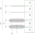
One or other method of fabricating n-type and p-type epitaxial regions (not shown) on a fin structure using a dual epitaxial growth process has limitations in application, as discussed below with respect to fig. 13. Fig. 13 shows device 100 with n-type finfet region 1358 and p-type finfet region 1360, respectively. Elements of device 100 that have the same reference numerals as elements of device 100 are similar in structure and function to those of device 100. The device 100 is shown after etching the spacer material layer 1312 from the sidewalls and top surface of the fin structure 1318 of the n-type finfet region 1358. A patterned photoresist layer 1362 is formed over the structure of the p-type finfet region 1360 before etching the spacer material layer 1312 from the fin structure 1318 to avoid etching the spacer material layer 1312 over the fin structure 1314. The layer 1312 of gap-wall material on the fin structure 1314 helps to prevent the growth of an n-type epitaxial region on the fin structure 1314 during the subsequent growth of the n-type epitaxial region on the fin structure 1318.
However, the use of a photoresist layer during the etching of the spacer material layer 1312 may adversely affect the structural integrity (e.g., fin structures 1314 and 1318, sti regions 108, and/or spacer material layer 1312 on structure 210.6). The material of the photoresist layer 1362 reacts with the etchant used for the etching process and reduces the selectivity of the etchant to the spacer material layer 1312 compared to the selectivity to the material of the fin structure 1318. Thus, material of the fin structures 1318 is lost when the spacer material layer 1312 is etched. The reaction of the etchant with the material of photoresist layer 1362 also results in the loss and damage of spacer material layer 1312 over fin structure 1314. Thus, when a subsequent n-type epitaxial region is grown on fin structure 1318, fin structure 1314 is not protected when the n-type epitaxial region is grown. In addition, due to the reaction of the etchant with the material of the photoresist layer 1362, the micro-trenches such as the micro-trench 1364 shown in fig. 13 are formed on the spacer material layer 1312, thereby causing damage to the spacer structure formed in the subsequent process from the spacer material layer 1312.
Thus, in the above-described methods of fabricating p-type and n-type finfets of device 100, the lack of a photoresist layer helps overcome some of the limitations in other methods of fabricating p-type and n-type finfets while simultaneously etching the spacer material from the fin structure.
Exemplary operation of a manufacturing apparatus
Fig. 14 is a flow chart of an exemplary method 1400 of manufacturing the device 100. For illustrative purposes only, the operations shown in fig. 14 are described with reference to the exemplary processes illustrated in fig. 2A-12A, 2B-12B, and 2C-12C. The above operations may be performed in a different order or not depending on the application. It is noted that the method 1400 does not produce a complete device 100. Accordingly, it is understood that additional processes may be provided before, during, and after the method 1400, and that some additional processes will only be briefly described herein.
In operation 1410, a layer of spacer material is deposited over the fin structures and the patterned structures. For example, a layer of spacer material may be blanket deposited over fin structures 114.1 through 114.4, fin structures 118.1 through 118.4, and patterned structures 210.1 through 210.6. The spacer material layer 312 is deposited in two stages by any suitable deposition process, such as chemical vapor deposition or atomic layer deposition. In the first deposition stage, the spacer material layer 312 is deposited to a thickness ranging from about 3nm to about 5 nm. During the second deposition phase, the spacer material layer 312 is deposited to a thickness ranging from about 4nm to about 6nm, so as to achieve a final thickness 312t ranging from about 7nm to about 10 nm.
In operation 1415, a layer of spacer material is etched back from the top surface and sidewalls of the fin structures. For example, the spacer material layer 312 may be etched back from the fin structure 114.1 to the top surface and sidewalls of the fin structure 118.1. An etch back of spacer material layer 312 from fin structure 114.1 to fin structure 118.1 may be performed simultaneously. In some embodiments, the spacer material layer 312 may be etched back by a dry etching process (e.g., reactive ion etching or other dry etching process using chlorine or fluorine-containing etchant). In some embodiments, the spacer material layer 312 is etched back by a cyclic deposition and etching process. In this cyclic process, one or more cycles of the deposition of the carbon-containing polymer may be followed by a dry etch process using a chlorine or fluorine-containing etchant as described above.
In operation 1420, a multi-layer hardmask is deposited over the fin structure etched back in operation 1415, and a layer of spacer material is deposited over the patterned structure. For example, a hard mask layer 552 is deposited over fin structures 114.1 through 118.1, and a spacer material layer 312 is deposited over structure 210.1. The hard mask layer 552 may comprise one or more layers of insulating material. In some embodiments, the hard mask layer 552 may comprise a first hard mask layer 554 and a second hard mask layer 556, respectively. The first hard mask layer 554 may comprise an oxide material (e.g., silicon oxide), and the second hard mask layer 556 may comprise an oxide material (e.g., aluminum oxide, zirconium dioxide, and/or lanthanum oxide), a nitride material (e.g., aluminum oxynitride and/or titanium nitride), or combinations thereof. In some embodiments, the blanket deposition of the first and second hard mask layers 554 and 556 may be performed using any suitable deposition process (e.g., chemical vapor deposition or atomic layer deposition).
In operation 1425, a photoresist layer over the p-type finfet region is patterned and the multi-layer hardmask in the n-type finfet region is etched. For example, the photoresist layer 662 over the p-type finfet region 660 may be patterned and the hard mask layer 552 in the n-type finfet region 658 may be etched. The second hard mask layer 556 of the hard mask layer 552 may be etched by a dry etching process using an etching gas, such as carbon tetrafluoride. The etchant gas used for the dry etching of the second hard mask layer 556 has a selectivity of the material of the second hard mask layer 556 to the first hard mask material layer 554 of equal to or greater than about 50: 1. by using an etchant gas [ e.g., (i) ammonia (NH) ]3) And hydrogen peroxide (H)2O2) (ii) sulfuric acid (H)2SO4) And (iii) DHF]The first hard mask layer 554 of the hard mask layer 552 is etched by the wet etching process of (1). The etchant used for the wet etching of the first hard mask layer 554 has a selectivity of the first hard mask layer 554 material to the spacer material layer 312 underlying the first hard mask layer 554 of equal to or greater than about 50: 1. the spacer material layer 312 may act as an etch stop layer during the wet etching of the first hard mask layer 554.
In operation 1430, an n-type epitaxial region is grown on the etched-back fin structure in the n-type finfet region. For example, an n-type epi region 120.1 is grown over the fin structure 118.1 in the n-type finfet region 658. The photoresist layer 662 in the p-type finfet region 660 is removed by a wet etch process prior to the formation of the n-type epitaxial region 120.1. An epitaxially grown n-type epitaxial region 120.1 is on a portion of the fin structure 118.1, wherein the portion of the fin structure 118.1 extends above the shallow trench isolation region 108 and is not below the structures 210.1-210.6. In some embodiments, the growth may be by (i) chemical vapor deposition, such as low pressure chemical vapor deposition, atomic layer chemical vapor deposition, ultra high vacuum chemical vapor deposition, reduced pressure chemical vapor deposition, or any suitable chemical vapor deposition; (ii) a molecular beam epitaxy process; (iii) any suitable epitaxial process; or (iv) the composite grown epitaxial region 120.1 described above.
In operation 1435, the multi-layer hard mask layer in the p-type finfet region is etched. For example, etching the hardmask layer 552 in the p-type finfet region 660 is performed by etching the hardmask layer 552 in the n-type finfet region 658 in a manner similar to that described in operation 1425.
In operation 1440, a multi-layer hardmask layer is deposited over the etched-back fin structure in the p-type finfet region and the n-type epi region in operation 1430. For example, a hardmask layer 952 may be deposited over the fin structure 114.1 in the p-type finfet region 660 and over the n-type finfet region 120.1. The hard mask layer 952 may include a first hard mask layer 954 and a second hard mask layer 956, respectively. The first and second hard mask layers 954, 956 are similar in structure, composition, and function to the first and second hard mask layers 554, 556, respectively.
In operation 1445, a photoresist layer is patterned over the n-type finfet region, and the multi-layer hard mask of operation 1440 in the p-type finfet region is etched. For example, a photoresist layer 1062 is patterned over the n-type finfet region 658, and a hard mask layer 952 is etched from the p-type finfet region 660. The hard mask layer 952 is etched in the p-type finfet region 660 by etching the hard mask layer 552 in the n-type finfet region 658 in a similar manner as described in operation 1425.
In operation 1450, a p-type epitaxial region is grown over the etched-back fin structure in the p-type finfet region. For example, a p-type epi region 116.1 may be grown over the fin structure 114.1 in the p-type finfet region 660. The photoresist layer 1062 in the n-type finfet region 658 is removed by a wet etch process prior to the formation of the p-type epitaxial region 116.1. A p-type epitaxial region 116.1 is epitaxially grown on a portion of the fin structure 114.1, wherein the portion of the fin structure 114.1 extends above the shallow trench isolation region 108 and not below the structures 210.1-210.6. In some embodiments, the growth may be by (i) chemical vapor deposition, such as low pressure chemical vapor deposition, atomic layer chemical vapor deposition, ultra high vacuum chemical vapor deposition, reduced pressure chemical vapor deposition, or any suitable chemical vapor deposition; (ii) a molecular beam epitaxy process; (iii) any suitable epitaxial process; or (iv) the composite grown epitaxial region 116.1 described above. The p-type epitaxial region 116.1 may comprise silicon germanium and may be doped in situ with a p-type dopant, such as boron, indium or gallium, during the epitaxial growth process.
In operation 1455, the multi-layer hard mask layer in the n-type finfet region is etched. For example, the hard mask layer 952 is etched in the n-type finfet region 658 by etching the hard mask layer 552 in the n-type finfet region 658 in a similar manner as described in operation 1425.
Illustrative embodiments and benefits
The above embodiments describe the fabrication of an n-type epitaxial region (e.g., region 120.1) on a fin structure (e.g., 118.1) and a p-type epitaxial region (e.g., region 116.1) on other fin structures (e.g., 114.1) using a dual epitaxial growth process. This embodiment provides a high degree of selectivity and conformal growth of n-type and p-type epitaxial regions on the fin structure. The dual epitaxial growth achieves a substantial reduction or minimization of the disruption of the structural and functional integrity of the fin structure. Some examples are described below.
A method of fabricating a semiconductor device includes forming first fin structures and second fin structures on a substrate, and forming patterned polysilicon structures on first portions of the first fin structures and on first portions of the second fin structures. The method further includes depositing an insulating layer over the second portions of the first fin structures and the second fin structures and over the patterned polysilicon structures, then selectively removing the insulating layer from the second portions of the first fin structures and the second fin structures, and patterning a first hard mask layer over the second portions of the second fin structures. The method also includes growing a first epitaxial region having a first type of conductivity on the second portion of the first fin structure, removing the patterned first hard mask layer from the second portion of the second fin structure, patterning a second hard mask layer on the first epitaxial region, and growing a second epitaxial region having a second type of conductivity on the second portion of the second fin structure. The second type of conductivity is different from the first type of conductivity.
In some embodiments, the selectively removing the insulating layer includes depositing a polymer layer on the patterned polysilicon structure and etching the insulating layer from the second portions of the first fin structures and the second fin structures.
In some embodiments, the patterning the first hard mask layer includes depositing a first hard mask layer over the second portion of the first fin structure and the second portion of the second fin structure, patterning a photoresist layer over the second portion of the second fin structure, and etching the first hard mask layer from the second portion of the first fin structure.
In some embodiments, the patterning the first hard mask layer includes depositing a first insulating layer over the second portion of the first fin structure and the second portion of the second fin structure, depositing a second insulating layer over the first insulating layer, patterning a photoresist layer over the second portion of the second fin structure, and etching the first insulating layer and the second insulating layer from the second portion of the first fin structure. The first insulating layer has a first material and the second insulating layer has a second material, and the second material is different from the first material.
In some embodiments, growing the first epitaxial region includes epitaxially growing a semiconductor material on the second portion of the first fin structure and in-situ doping the semiconductor material with dopants. The dopant has a first type conductivity.
In some embodiments, removing the patterned first hard mask layer comprises dry etching the first layer of the first hard mask layer and wet etching the second layer of the first hard mask layer.
In some embodiments, growing the second epitaxial region includes epitaxially growing a semiconductor material on the second portion of the second fin structure and in-situ doping the semiconductor material with dopants having the second type of conductivity.
In some embodiments, growing the first epitaxial region includes epitaxially growing a first region on the second portion of the first fin structure, epitaxially growing a second region on the first region, and epitaxially growing a third region on the second region. The first region has a first dopant concentration, the second region has a second dopant concentration, and the third region has a third dopant concentration, wherein the first, second, and third dopant concentrations are different from each other.
In some embodiments, growing the second epitaxial region includes epitaxially growing a first region on the second portion of the second fin structure, epitaxially growing a second region on the first region, and epitaxially growing a third region on the second region. The first region has a first germanium atom concentration, the second region has a second germanium atom concentration, and the third region has a third germanium atom concentration, wherein the first germanium atom concentration, the second germanium atom concentration, and the third germanium atom concentration are different from each other.
In some embodiments, the insulating layer comprises a low-k material.
In some embodiments, the method further includes laterally trimming the second portions of the first fin structures and the second fin structures after the operation of selectively removing the insulating layer.
A method of fabricating a semiconductor device includes forming first fin structures and second fin structures on a substrate, and forming patterned polysilicon structures on first portions of the first fin structures and on first portions of the second fin structures. The method further includes depositing an insulating layer over the second portions of the first fin structures and the second fin structures and over the patterned polysilicon structures, and then etching the insulating layer from the second portions of the first fin structures and the second portions of the second fin structures, laterally trimming the first fin structures and the etched second portions of the second fin structures, and patterning a first hard mask layer over the trimmed second portions of the second fin structures. The method also includes growing a first epitaxial region having a first type of conductivity on the trimmed second portion of the first fin structure, patterning a second hardmask layer on the first epitaxial region, and growing a second epitaxial region having a second type of conductivity on the trimmed second portion of the second fin structure. The second type of conductivity is different from the first type of conductivity.
In some embodiments, the laterally trimming operation includes oxidizing surfaces of sidewalls of the second portions of the first fin structures and the second portions of the second fin structures.
In some embodiments, the patterning the first hard mask layer includes depositing a first insulating layer over the trimmed second portions of the first fin structures and the trimmed second portions of the second fin structures, depositing a second insulating layer over the first insulating layer, patterning a photoresist layer over the trimmed second portions of the second fin structures, and etching the first insulating layer and the second insulating layer from the trimmed second portions of the first fin structures. The first insulating layer has a first material and the second insulating layer has a second material, and the second material is different from the first material.
In some embodiments, the method further comprises removing the patterned first hard mask layer from the trimmed second portion of the second fin structure prior to the operation of patterning the second hard mask layer on the first epitaxial region.
In some embodiments, removing the patterned first hard mask layer from the trimmed second portions of the second fin structures includes dry etching a first layer of the first hard mask layer and wet etching a second layer of the first hard mask layer.
A method of fabricating a semiconductor device includes forming first and second fin structures on a substrate and depositing an insulating layer on the first and second fin structures. The method also includes etching an insulating layer from the first fin structure and the second fin structure, and patterning a first hard mask layer on the second fin structure. The method also includes growing a first epitaxial region having a first type of conductivity on the first fin structure, removing the patterned first hard mask layer from the second fin structure, patterning a second hard mask layer on the first epitaxial region, and growing a second epitaxial region having a second type of conductivity on the second fin structure. The second type of conductivity is different from the first type of conductivity.
In some embodiments, growing the first epitaxial region includes epitaxially growing a first region on the first fin structure, epitaxially growing a second region on the first region, and epitaxially growing a third region on the second region. The first region has a first dopant concentration, the second region has a second dopant concentration, and the third region has a third dopant concentration, wherein the first, second, and third dopant concentrations are different from each other.
In some embodiments, growing the second epitaxial region includes epitaxially growing a first region on the second fin structure, epitaxially growing a second region on the first region, and epitaxially growing a third region on the second region. The first region has a first concentration of germanium atoms, the second region has a second concentration of germanium atoms, and the third region has a third concentration of germanium atoms, wherein the first concentration of germanium atoms, the second concentration of germanium atoms, and the third concentration of germanium atoms are different from each other.
In some embodiments, the method further comprises laterally trimming the first fin structures and the second fin structures after the operation of etching the insulating layer.
The foregoing summary, as well as the following detailed description of the embodiments, is provided to enable one of ordinary skill in the art to make and use the present disclosure. Those skilled in the art should appreciate that they may readily use the present disclosure as a basis for designing or modifying other processes and structures for carrying out the same purposes and/or achieving the same advantages of the embodiments introduced herein. Those skilled in the art should also realize that such equivalent constructions do not depart from the spirit and scope of the present disclosure, and that they may make various changes, substitutions, and alterations herein without departing from the spirit and scope of the present disclosure.