CN108091629B - Photoelectric chip integrated structure - Google Patents
Photoelectric chip integrated structure Download PDFInfo
- Publication number
- CN108091629B CN108091629B CN201711305080.1A CN201711305080A CN108091629B CN 108091629 B CN108091629 B CN 108091629B CN 201711305080 A CN201711305080 A CN 201711305080A CN 108091629 B CN108091629 B CN 108091629B
- Authority
- CN
- China
- Prior art keywords
- chip
- optoelectronic chip
- optoelectronic
- package body
- pad
- Prior art date
- Legal status (The legal status is an assumption and is not a legal conclusion. Google has not performed a legal analysis and makes no representation as to the accuracy of the status listed.)
- Active
Links
Images


Classifications
-
- H10W72/07251—
-
- H10W72/20—
Landscapes
- Light Receiving Elements (AREA)
Abstract
本发明公开了一种光电芯片集成结构,包括:光电芯片和电芯片;所述光电芯片和所述电芯片中的一者正装设置,另一者倒装设置;所述光电芯片的至少一个第一焊盘对应于所述电芯片的至少一个第二焊盘设置。本发明通过正装和倒装的不同方式使得光电芯片和电芯片的焊盘相对放置并位置对应,从而可以通过焊球连接相应的焊盘,或者焊盘之间直接键合连接或接触连接。相比于采用键合引线连接,焊球的横截面积或者直接结合的接触面积较大,因此电感较小,根据公式

The invention discloses an optoelectronic chip integrated structure, comprising: an optoelectronic chip and an electrical chip; one of the optoelectronic chip and the electrical chip is installed in a positive position, and the other is installed in a flip chip; at least one first part of the optoelectronic chip is installed A pad is arranged corresponding to at least one second pad of the electrical chip. In the present invention, the pads of the optoelectronic chip and the electric chip are placed oppositely and in corresponding positions through different methods of forward mounting and flipping, so that the corresponding pads can be connected by solder balls, or the pads can be directly bonded or contacted. The cross-sectional area of the solder ball or the contact area of the direct bond is larger than that of a bond wire connection, so the inductance is smaller, according to the formula
Description
技术领域technical field
本发明涉及芯片集成技术领域,具体涉及一种光电芯片集成结构。The invention relates to the technical field of chip integration, in particular to an optoelectronic chip integration structure.
背景技术Background technique
光通信(Optical Communication)是以光波为载波的通信方式。随着技术的发展,通信数据量越来越大,因此对光通信模块的传输速率要求越来越高。目前,56Gbps以及112Gbps是下一代光互连的标准。光电芯片集成结构是光通信模块的核心组成部分。光电芯片集成结构将光电芯片(例如激光器、调制器、探测器等有源光电芯片或多个结构的光电集成芯片)与其外围电路的电芯片(例如光电芯片的驱动芯片)集成在一起,实现光信号和电信号进行转换的功能。通信数据量本身越来越大,加之光电芯片与电芯片需要将光信号和电信号频繁进行转换,使得这二者之间互连的电特性成为光电芯片集成结构带宽设计的瓶颈。Optical communication is a communication method that uses light waves as carriers. With the development of technology, the amount of communication data is getting larger and larger, so the requirements for the transmission rate of optical communication modules are getting higher and higher. Currently, 56Gbps and 112Gbps are the next-generation optical interconnect standards. The optoelectronic chip integrated structure is the core component of the optical communication module. The optoelectronic chip integration structure integrates optoelectronic chips (such as active optoelectronic chips such as lasers, modulators, detectors, or optoelectronic integrated chips with multiple structures) and the electrical chips of its peripheral circuits (such as the driver chips of optoelectronic chips) to realize optical The function of converting signals and electrical signals. The amount of communication data itself is increasing, and the optoelectronic chip and the electrical chip need to frequently convert the optical signal and the electrical signal, making the electrical characteristics of the interconnection between the two become a bottleneck in the bandwidth design of the integrated structure of the optoelectronic chip.
现有方式往往将光电芯片和电芯片组织在介质基板上,并将其焊盘采用本领域技术人员在芯片集成时常用的键合引线的方式连接至介质基板的布线层上,以便在介质基板上统一布线。In the existing methods, optoelectronic chips and electrical chips are often organized on a dielectric substrate, and their pads are connected to the wiring layer of the dielectric substrate by means of bonding wires commonly used by those skilled in the art during chip integration, so that the unified wiring.
然而,发明人发现,现有方式实现光电芯片集成结构时所采用的键合引线使得光电芯片互连的带宽受到限制难以拓宽。However, the inventors found that the bonding wires used in realizing the integrated structure of the optoelectronic chip in the existing way limit the bandwidth of the interconnection of the optoelectronic chip and it is difficult to widen it.
发明内容SUMMARY OF THE INVENTION
有鉴于此,本发明实施例提供了一种光电芯片集成结构,以解决光电芯片互连的带宽受到限制难以拓宽的问题。In view of this, the embodiments of the present invention provide an optoelectronic chip integrated structure to solve the problem that the bandwidth of the optoelectronic chip interconnection is limited and difficult to widen.
本发明第一方面提供了一种光电芯片集成结构,包括:光电芯片和电芯片;所述光电芯片和所述电芯片中的一者正装设置,另一者倒装设置;所述光电芯片的至少一个第一焊盘对应于所述电芯片的至少一个第二焊盘设置。A first aspect of the present invention provides an optoelectronic chip integrated structure, comprising: an optoelectronic chip and an electrical chip; one of the optoelectronic chip and the electrical chip is installed in a front-mounted manner, and the other is installed in a flip-chip manner; At least one first pad is arranged corresponding to at least one second pad of the electrical chip.
可选地,所述光电芯片集成结构还包括:封装体;所述光电芯片正装嵌入设置在所述封装体中,所述光电芯片的第一表面与所述封装体的第一表面齐平;所述电芯片倒装设置在所述封装体的第一表面。Optionally, the optoelectronic chip integrated structure further includes: a package body; the optoelectronic chip is installed and embedded in the package body, and the first surface of the optoelectronic chip is flush with the first surface of the package body; The electrical chip is flip-chip disposed on the first surface of the package body.
可选地,所述光电芯片的光功能部件位于所述光电芯片的第一表面。Optionally, the optical functional components of the optoelectronic chip are located on the first surface of the optoelectronic chip.
可选地,所述封装体内设置有至少一个第一过孔,分别与所述电芯片的至少一个第三焊盘连接,所述第一过孔从所述封装体的第一表面延伸至第二表面。Optionally, the package body is provided with at least one first via hole, which is respectively connected to at least one third pad of the electrical chip, and the first via hole extends from the first surface of the package body to the first via hole. Second surface.
可选地,所述封装体内还嵌入设置有硬质块体,所述硬质块体外露的表面与所述封装体的表面齐平;所述硬质块体内设置有至少一个第一过孔,分别与所述电芯片的至少一个第三焊盘连接;所述第一过孔从所述硬质块体的第一表面延伸至第二表面。Optionally, a hard block body is also embedded in the package body, and the exposed surface of the hard block body is flush with the surface of the package body; at least one first via hole is provided in the hard block body , respectively connected to at least one third pad of the electrical chip; the first via hole extends from the first surface to the second surface of the hard block.
可选地,所述第一过孔与所述第三焊盘直接连接。Optionally, the first via hole is directly connected to the third pad.
可选地,所述光电芯片集成结构还包括:第一布线层,设置于所述封装体的第一表面;所述第一布线层的导线的一端分别与所述电芯片的至少一个第三焊盘连接,或者所述第一布线层的导线的一端分别与所述光电芯片的至少一个第四焊盘连接;另一端与所述第一过孔连接。Optionally, the optoelectronic chip integrated structure further includes: a first wiring layer disposed on the first surface of the package body; one end of the wire of the first wiring layer is respectively connected with at least one third part of the electrical chip. The pads are connected, or one end of the wire of the first wiring layer is respectively connected to at least one fourth pad of the optoelectronic chip; the other end is connected to the first via hole.
可选地,所述光电芯片集成结构还包括:第二布线层,设置于所述封装体的第二表面,所述第二布线层的导线一端与所述第一过孔连接,另一端设置焊球。Optionally, the optoelectronic chip integrated structure further includes: a second wiring layer disposed on the second surface of the package body, one end of the wire of the second wiring layer is connected to the first via hole, and the other end is disposed solder balls.
可选地,所述封装体的第二表面露出所述光电芯片的至少一个第五焊盘,并且在所述封装体的第二表面上对应于所述第五焊盘的位置设置有焊球。Optionally, at least one fifth pad of the optoelectronic chip is exposed on the second surface of the package body, and solder balls are provided on the second surface of the package body at positions corresponding to the fifth pads .
可选地,所述光电芯片内部设置有第二过孔,所述第二过孔的一端与所述光电芯片的焊盘连接,另一端延伸至所述光电芯片的第二表面连接焊球或布线层的导线。Optionally, a second via hole is provided inside the optoelectronic chip, one end of the second via hole is connected to the pad of the optoelectronic chip, and the other end extends to the second surface of the optoelectronic chip to connect to solder balls or Wires of the wiring layer.
本发明实施例所提供的光电芯片集成结构,通过正装和倒装的不同方式使得光电芯片和电芯片的焊盘相对放置并位置对应,从而可以通过焊球连接相应的焊盘,或者焊盘之间直接键合连接或接触连接。相比于采用键合引线连接,焊球的横截面积或者直接结合的接触面积较大,因此电感较小,根据公式电感越小,频率越高,因此,通过焊球连接或焊盘直接键合所能达到的频率较高,从而能够拓宽光电芯片与电芯片信号传输的带宽,其相对带宽可达传统封装的8至50倍。上述光电芯片集成结构大大缩短了走线长度,降低了信号延迟与损耗,In the optoelectronic chip integrated structure provided by the embodiment of the present invention, the pads of the optoelectronic chip and the optoelectronic chip are placed relative to each other and the positions correspond to each other by different methods of front loading and flipping, so that the corresponding pads can be connected by solder balls, or the pads between the pads can be connected by solder balls. direct bond connections or contact connections. The cross-sectional area of the solder ball or the contact area of the direct bond is larger than that of a bond wire connection, so the inductance is smaller, according to the formula The smaller the inductance, the higher the frequency. Therefore, the frequency that can be achieved by solder ball connection or direct bonding of pads is higher, which can broaden the bandwidth of signal transmission between optoelectronic chips and electrical chips, and its relative bandwidth can reach 8% of traditional packaging. to 50 times. The above-mentioned optoelectronic chip integrated structure greatly shortens the trace length, reduces the signal delay and loss,
附图说明Description of drawings
通过参考附图会更加清楚的理解本发明的特征和优点,附图是示意性的而不应理解为对本发明进行任何限制,在附图中:The features and advantages of the present invention will be more clearly understood by reference to the accompanying drawings, which are schematic and should not be construed as limiting the invention in any way, in which:
图1示出了根据本发明实施例的一种光电芯片集成结构的示意图;FIG. 1 shows a schematic diagram of an integrated structure of an optoelectronic chip according to an embodiment of the present invention;
图2示出了根据本发明实施例的再一种光电芯片集成结构的示意图;FIG. 2 shows a schematic diagram of yet another optoelectronic chip integrated structure according to an embodiment of the present invention;
图3示出了根据本发明实施例的又一种光电芯片集成结构的示意图;FIG. 3 shows a schematic diagram of yet another optoelectronic chip integrated structure according to an embodiment of the present invention;
图4示出了根据本发明实施例的又一种光电芯片集成结构的示意图;FIG. 4 shows a schematic diagram of yet another optoelectronic chip integrated structure according to an embodiment of the present invention;
图5示出了根据本发明实施例的又一种光电芯片集成结构的示意图。FIG. 5 shows a schematic diagram of yet another optoelectronic chip integrated structure according to an embodiment of the present invention.
具体实施方式Detailed ways
为了使本发明的目的、优点、制备方法更加清楚,下面将结合附图对本发明的实施示例进行详细描述,所述实施例的示例在附图中示出,其中附图中部分结构直接给出了优选的结构材料,显然,所描述的实施例是本发明一部分实施例,而不是全部的实施例。需要说明的是,参考附图描述的实施例是示例性的,实施例中表明的结构材料也是示例性的,仅用于解释本发明,而不能解释为对本发明的限制,本发明各个实施例的附图仅是为了示意的目的,因此没有必要按比例绘制。基于本发明中的实施例,本领域技术人员在没有作出创造性劳动前提下所获得的所有其他实施例,都属于本发明保护的范围。In order to make the purpose, advantages and preparation method of the present invention clearer, the following will describe the embodiments of the present invention in detail with reference to the accompanying drawings. In view of preferred materials of construction, it is apparent that the described embodiments are some, but not all, of the embodiments of the present invention. It should be noted that the embodiments described with reference to the accompanying drawings are exemplary, and the structural materials shown in the embodiments are also exemplary, and are only used to explain the present invention, but not to limit the present invention. The drawings are for illustrative purposes only and are not necessarily drawn to scale. Based on the embodiments of the present invention, all other embodiments obtained by those skilled in the art without creative efforts shall fall within the protection scope of the present invention.
实施例一Example 1
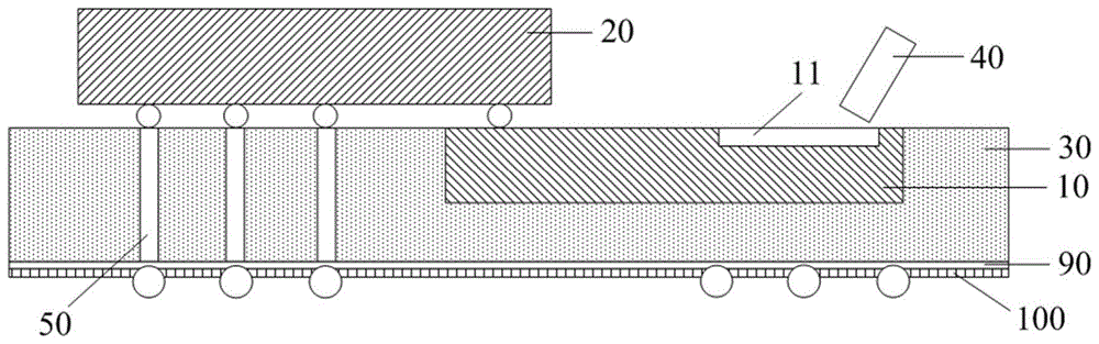
本发明实施例提供了一种光电芯片集成结构,该集成结构包括光电芯片10和电芯片20。光电芯片10和电芯片20中的一者正装设置,另一者倒装设置。光电芯片10的至少一个第一焊盘对应于电芯片20的至少一个第二焊盘设置。第一焊盘与第二焊盘可以通过焊球连接或者焊盘直接键合连接,本申请在此不对连接方式做限定。The embodiment of the present invention provides an optoelectronic chip integrated structure, and the integrated structure includes an
上述光电芯片集成结构,通过正装和倒装的不同方式使得光电芯片和电芯片的焊盘相对放置并位置对应,从而可以通过焊球连接相应的焊盘,或者焊盘之间直接键合连接或接触连接。相比于采用键合引线连接,焊球的横截面积或者直接结合的接触面积较大,因此电感较小,根据公式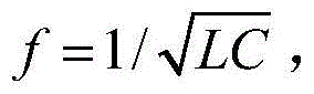
本申请中的光电芯片10可以为激光器、调制器、探测器等有源光电芯片或多个结构的光电集成芯片,材料可以是硅光芯片,也可以是铟、镓、砷、磷等化合物半导体材料,或者碳化硅、氮化硅材料。The
作为本实施例的一种可选实施方式,如图1所示,该光电芯片集成结构包括封装体30,例如塑封体。本申请中所述的“封装体”为软质的封装胶体固化后所形成的块体。光电芯片10正装嵌入设置在封装体30中,光电芯片10的第一表面与封装体30的第一表面齐平。例如可以先在衬底上涂覆软质的封装胶,再将光电芯片10嵌入放置在封装胶体,封装胶包覆光电芯片10,待封装胶固化之后将第一表面磨平,或者在封装胶固化之前将第一表面整平。封装体30能够与光电芯片10直接无缝粘接,从而能够精确地固定光电芯片10的位置以及水平度,便于其他部件能够基于光电芯片10精准贴装。As an optional implementation manner of this embodiment, as shown in FIG. 1 , the optoelectronic chip integrated structure includes a
作为采用塑封体30固定光电芯片10的一种变形方式,可以在硬质的块体中开设凹槽,再在凹槽底部涂覆胶体,将光电芯片10粘贴在凹槽底部。然而这种实施方式对于凹槽开设的深度及底部水平度要求较高,一般工艺难以达到非常精准的要求;此外光电芯片10只有底部固定,在后续工艺步骤中不够稳定。As a modification of using the
电芯片20倒装设置在封装体30的第一表面。本申请中所述的“倒装”是指焊盘朝下的设置,“正装”为焊盘朝上的设置。The
光电芯片10上具有光耦合结构等光功能部件11,例如可以为光栅、模斑转换器或者波导结构。可选地,光电芯片10的光功能部件11位于光电芯片10的第一表面,从而便于光功能部件11与其他部件(例如光纤40)的连接。The
电芯片20还具有第三焊盘,与第二焊盘位于电芯片20的同一表面,第三焊盘可以通过封装体30第一表面布线层的导线引出,并在导线端点处设置焊球。或者,作为本实施例的一种可选实施方式,封装体30内设置有至少一个第一过孔50,分别与电芯片20的至少一个第三焊盘连接,第一过孔50从封装体30的第一表面延伸至第二表面。第一过孔50可以与第三焊盘通过焊球直接连接。The
本申请中的“过孔”也称金属化孔,为连通第一表面和第二表面的印制导线,在表面需要连通的导线的交汇处或者焊球位置钻上一个公共孔,再在过孔的孔壁圆柱面上用化学沉积的方法镀上一层金属。The "via hole" in this application is also called a metallized hole, which is a printed wire connecting the first surface and the second surface. A common hole is drilled at the intersection of the wires that need to be connected on the surface or at the position of the solder ball, and then a common hole is drilled on the surface. A layer of metal is plated on the cylindrical surface of the hole wall of the hole by chemical deposition.
作为上述可选实施方式的一种并列可选实施方式,如图2所示,封装体30内还嵌入设置有硬质块体60,硬质块体60外露的表面与封装体30的表面齐平。硬质块体60内设置有至少一个第一过孔50,分别与电芯片20的至少一个第三焊盘连接。第一过孔50从硬质块体60的第一表面延伸至第二表面。第一过孔50可以与第三焊盘接连接,二者之间可以设置焊球辅助连接。As a side-by-side optional embodiment of the above-mentioned optional embodiments, as shown in FIG. 2 , the
可选地,该光电集成结构还包括第一布线层70,如图4所示,设置于封装体30的第一表面。第一布线层70的导线的一端分别与电芯片20的至少一个第三焊盘连接(图中未示出该情形);或者,第一布线层70的导线的一端分别与光电芯片10的至少一个第四焊盘(如图4中12所示)连接。第一布线层70的导线的另一端与第一过孔50连接。可选地,还可以通过如图5所示的布线块120代替第一布线层70,也即预先将布线结构设置在布线块120上,在制作光电芯片集成结构时直接将布线块120用于组装即可。通过第一布线层或该布线块,将光电芯片或电芯片的焊盘扇出设计,可以便于光电集成结构布线。第一布线层70的表面还可以设置绝缘层80。Optionally, the optoelectronic integrated structure further includes a first wiring layer 70 , as shown in FIG. 4 , disposed on the first surface of the
可选地,该光电芯片集成结构还包括第二布线层90,设置于封装体30的第二表面,第二布线层90的导线一端与第一过孔50连接,另一端设置焊球。通过第二布线层,可以使得焊球在封装体的第二表面较为均匀分布,以均衡总体电特性。第二布线层90的表面还可以设置绝缘层100。Optionally, the optoelectronic chip integrated structure further includes a
作为本实施例的一种可选实施方式,如图3所示,封装体30的第二表面通过减薄工艺露出光电芯片10的至少一个第五焊盘,并且在封装体30的第二表面上对应于第五焊盘的位置设置有焊球,从而可以将光电芯片10第二表面的信号(例如低频信号)直接引出,便于光电芯片集成结构布线。As an optional implementation of this embodiment, as shown in FIG. 3 , at least one fifth pad of the
可选地,光电芯片10内部设置有第二过孔110,第二过孔110的一端与光电芯片10的焊盘连接,另一端延伸至光电芯片10的第二表面连接焊球或布线层的导线。通过在光电芯片10内部设置第二过孔,可以将光电芯片10第一表面的信号直接引出,便于光电芯片集成结构布线。Optionally, a second via
虽然关于示例实施例及其优点已经详细说明,但是本领域技术人员可以在不脱离本发明的精神和所附权利要求限定的保护范围的情况下对这些实施例进行各种变化、替换和修改,这样的修改和变型均落入由所附权利要求所限定的范围之内。对于其他例子,本领域的普通技术人员应当容易理解在保持本发明保护范围内的同时,工艺步骤的次序可以变化。Although the exemplary embodiments and their advantages have been described in detail, those skilled in the art can make various changes, substitutions and alterations in these embodiments without departing from the spirit of the invention and the scope of protection defined by the appended claims, Such modifications and variations are within the scope defined by the appended claims. For other examples, those of ordinary skill in the art will readily understand that the order of the process steps may be varied while remaining within the scope of the present invention.
此外,本发明的应用范围不局限于说明书中描述的特定实施例的工艺、机构、制造、物质组成、手段、方法及步骤。从本发明的公开内容,作为本领域的普通技术人员将容易地理解,对于目前已存在或者以后即将开发出的工艺、机构、制造、物质组成、手段、方法或步骤,其中它们执行与本发明描述的对应实施例大体相同的功能或者获得大体相同的结果,依照本发明可以对它们进行应用。因此,本发明所附权利要求旨在将这些工艺、机构、制造、物质组成、手段、方法或步骤包含在其保护范围内。Furthermore, the scope of application of the present invention is not limited to the process, mechanism, manufacture, composition of matter, means, method and steps of the specific embodiments described in the specification. From the disclosure of the present invention, as those of ordinary skill in the art, it will be easily understood by those of ordinary skill in the art that there are currently existing or will be developed in the future for the process, mechanism, manufacture, composition of matter, means, method or step, wherein they perform the same as the present invention. Corresponding embodiments described that function substantially the same or achieve substantially the same results can be applied in accordance with the present invention. Accordingly, the appended claims of this invention are intended to include within their scope such processes, mechanisms, manufacture, compositions of matter, means, methods, or steps.
Claims (9)
Priority Applications (1)
| Application Number | Priority Date | Filing Date | Title |
|---|---|---|---|
| CN201711305080.1A CN108091629B (en) | 2017-12-08 | 2017-12-08 | Photoelectric chip integrated structure |
Applications Claiming Priority (1)
| Application Number | Priority Date | Filing Date | Title |
|---|---|---|---|
| CN201711305080.1A CN108091629B (en) | 2017-12-08 | 2017-12-08 | Photoelectric chip integrated structure |
Publications (2)
| Publication Number | Publication Date |
|---|---|
| CN108091629A CN108091629A (en) | 2018-05-29 |
| CN108091629B true CN108091629B (en) | 2020-01-10 |
Family
ID=62174717
Family Applications (1)
| Application Number | Title | Priority Date | Filing Date |
|---|---|---|---|
| CN201711305080.1A Active CN108091629B (en) | 2017-12-08 | 2017-12-08 | Photoelectric chip integrated structure |
Country Status (1)
| Country | Link |
|---|---|
| CN (1) | CN108091629B (en) |
Families Citing this family (14)
| Publication number | Priority date | Publication date | Assignee | Title |
|---|---|---|---|---|
| CN109786368A (en) * | 2019-01-24 | 2019-05-21 | 中国科学院微电子研究所 | A kind of photoelectric chip collaboration encapsulating structure and method |
| CN110890349B (en) * | 2019-12-20 | 2025-03-07 | 华进半导体封装先导技术研发中心有限公司 | A three-dimensional packaging structure of an optoelectronic chip with an optical interconnection interface and a manufacturing method thereof |
| CN112285850A (en) * | 2020-10-21 | 2021-01-29 | 希烽光电科技(南京)有限公司 | Silicon optical engine with high bandwidth and low optical loss |
| CN113589449A (en) * | 2021-06-21 | 2021-11-02 | 北京协同创新研究院 | Hybrid integrated system applied to photoelectric interconnection |
| CN114325965B (en) * | 2021-12-28 | 2024-05-28 | 华进半导体封装先导技术研发中心有限公司 | Packaging structure of optical chip and electric chip and preparation method thereof |
| CN114355520A (en) * | 2021-12-30 | 2022-04-15 | 华进半导体封装先导技术研发中心有限公司 | Optical chip and electric chip packaging structure and preparation method thereof |
| CN115149394B (en) * | 2022-09-05 | 2022-11-15 | 山东中清智能科技股份有限公司 | Photoelectric device integrated packaging structure and manufacturing method thereof |
| WO2024066360A1 (en) * | 2022-09-30 | 2024-04-04 | 青岛海信宽带多媒体技术有限公司 | Optical module |
| CN116646346A (en) * | 2023-06-12 | 2023-08-25 | Nano科技(北京)有限公司 | An optoelectronic packaging structure for optoelectronic hybrid integration |
| CN117594451A (en) * | 2023-10-20 | 2024-02-23 | 盛合晶微半导体(江阴)有限公司 | Optoelectronic integrated semiconductor packaging structure and preparation method thereof |
| CN117096037B (en) * | 2023-10-20 | 2023-12-22 | 盛合晶微半导体(江阴)有限公司 | Semiconductor photoelectric packaging structure based on grating and preparation method thereof |
| CN117476472A (en) * | 2023-10-20 | 2024-01-30 | 盛合晶微半导体(江阴)有限公司 | Optoelectronic integrated semiconductor packaging structure and preparation method thereof |
| CN118507361A (en) * | 2023-10-20 | 2024-08-16 | 盛合晶微半导体(江阴)有限公司 | Semiconductor photoelectric packaging structure based on grating and preparation method thereof |
| CN117878111A (en) * | 2024-01-11 | 2024-04-12 | 华进半导体封装先导技术研发中心有限公司 | A photoelectric sealing structure and preparation method thereof |
Citations (4)
| Publication number | Priority date | Publication date | Assignee | Title |
|---|---|---|---|---|
| CN1835229A (en) * | 2005-03-16 | 2006-09-20 | 索尼株式会社 | Semiconductor device and method of manufacturing semiconductor device |
| CN102460690A (en) * | 2009-06-24 | 2012-05-16 | 英特尔公司 | Multi-chip package and method of providing die-to-die interconnects in same |
| CN103885141A (en) * | 2012-12-19 | 2014-06-25 | 深圳新飞通光电子技术有限公司 | Planar optical waveguide type parallel optical assembly and optical module |
| CN106980159A (en) * | 2017-03-07 | 2017-07-25 | 中国科学院微电子研究所 | Photoelectric module packaging structure based on photoelectric hybrid integration |
Family Cites Families (3)
| Publication number | Priority date | Publication date | Assignee | Title |
|---|---|---|---|---|
| US7247932B1 (en) * | 2000-05-19 | 2007-07-24 | Megica Corporation | Chip package with capacitor |
| US6659512B1 (en) * | 2002-07-18 | 2003-12-09 | Hewlett-Packard Development Company, L.P. | Integrated circuit package employing flip-chip technology and method of assembly |
| JP4380130B2 (en) * | 2002-09-13 | 2009-12-09 | ソニー株式会社 | Semiconductor device |
-
2017
- 2017-12-08 CN CN201711305080.1A patent/CN108091629B/en active Active
Patent Citations (4)
| Publication number | Priority date | Publication date | Assignee | Title |
|---|---|---|---|---|
| CN1835229A (en) * | 2005-03-16 | 2006-09-20 | 索尼株式会社 | Semiconductor device and method of manufacturing semiconductor device |
| CN102460690A (en) * | 2009-06-24 | 2012-05-16 | 英特尔公司 | Multi-chip package and method of providing die-to-die interconnects in same |
| CN103885141A (en) * | 2012-12-19 | 2014-06-25 | 深圳新飞通光电子技术有限公司 | Planar optical waveguide type parallel optical assembly and optical module |
| CN106980159A (en) * | 2017-03-07 | 2017-07-25 | 中国科学院微电子研究所 | Photoelectric module packaging structure based on photoelectric hybrid integration |
Also Published As
| Publication number | Publication date |
|---|---|
| CN108091629A (en) | 2018-05-29 |
Similar Documents
| Publication | Publication Date | Title |
|---|---|---|
| CN108091629B (en) | Photoelectric chip integrated structure | |
| TWI781650B (en) | Photonic semiconductor device and method of manufacture | |
| TWI813229B (en) | Package and method forming same | |
| US8884429B2 (en) | Package structure having embedded electronic component and fabrication method thereof | |
| CN110310932A (en) | A kind of integrated encapsulation structure and manufacturing method of optical chip and electrical chip | |
| JP6942310B2 (en) | Embedded semiconductor package and its method | |
| CN110299329A (en) | A kind of encapsulating structure and preparation method thereof, electronic equipment | |
| US11183474B2 (en) | Electronic device package and method for manufacturing the same | |
| CN102782838B (en) | Embedded chip package | |
| US20060198570A1 (en) | Hybrid module and production method for same, and hybrid circuit device | |
| US20250286341A1 (en) | Method for preparing optoelectronic integrated semiconductor packaging structure | |
| CN209880613U (en) | Three-dimensional integrated packaging structure of optical chip and electric chip | |
| TW202109746A (en) | Electronic package and method for fabricating the same | |
| CN115516629B (en) | Optoelectronic device and optoelectronic integrated structure | |
| US9331051B2 (en) | Wafer scale technique for interconnecting vertically stacked dies | |
| TWI701779B (en) | Electronic packaging structure and manufacturing method thereof | |
| US12224267B2 (en) | Chip interconnecting method, interconnect device and method for forming chip packages | |
| CN115632072A (en) | High-density photoelectric co-packaging structure and packaging method for silicon optical chip | |
| CN110828443A (en) | Substrate-free optoelectronic hybrid integrated structure and preparation method thereof | |
| CN105810705B (en) | Packaging structure of high-pixel image sensor chip and method of making the same | |
| WO2023087323A1 (en) | Photoelectric transceiver assembly and method for manufacturing same | |
| KR20250052553A (en) | Semiconductor package | |
| CN203871322U (en) | Silicon through hole device applied to high speed broadband optical interconnection | |
| CN218887173U (en) | Semiconductor packaging device | |
| TWI892435B (en) | Package structure including at least two electronic components and method of manufacturing the same |
Legal Events
| Date | Code | Title | Description |
|---|---|---|---|
| PB01 | Publication | ||
| PB01 | Publication | ||
| SE01 | Entry into force of request for substantive examination | ||
| SE01 | Entry into force of request for substantive examination | ||
| GR01 | Patent grant | ||
| GR01 | Patent grant |