CN107910351B - Manufacturing method of TFT substrate - Google Patents
Manufacturing method of TFT substrate Download PDFInfo
- Publication number
- CN107910351B CN107910351B CN201711124844.7A CN201711124844A CN107910351B CN 107910351 B CN107910351 B CN 107910351B CN 201711124844 A CN201711124844 A CN 201711124844A CN 107910351 B CN107910351 B CN 107910351B
- Authority
- CN
- China
- Prior art keywords
- oxide semiconductor
- layer
- semiconductor layer
- tft substrate
- line
- Prior art date
- Legal status (The legal status is an assumption and is not a legal conclusion. Google has not performed a legal analysis and makes no representation as to the accuracy of the status listed.)
- Active
Links
- 239000000758 substrate Substances 0.000 title claims abstract description 91
- 238000004519 manufacturing process Methods 0.000 title claims abstract description 45
- 239000004065 semiconductor Substances 0.000 claims abstract description 93
- 238000000034 method Methods 0.000 claims abstract description 66
- 230000008569 process Effects 0.000 claims abstract description 35
- 239000010410 layer Substances 0.000 claims description 199
- 229920002120 photoresistant polymer Polymers 0.000 claims description 51
- 238000000151 deposition Methods 0.000 claims description 31
- 239000002184 metal Substances 0.000 claims description 19
- 238000000059 patterning Methods 0.000 claims description 14
- XKRFYHLGVUSROY-UHFFFAOYSA-N Argon Chemical compound [Ar] XKRFYHLGVUSROY-UHFFFAOYSA-N 0.000 claims description 10
- 239000011241 protective layer Substances 0.000 claims description 9
- 239000007789 gas Substances 0.000 claims description 7
- 238000005240 physical vapour deposition Methods 0.000 claims description 6
- 229910052786 argon Inorganic materials 0.000 claims description 5
- 239000001307 helium Substances 0.000 claims description 5
- 229910052734 helium Inorganic materials 0.000 claims description 5
- SWQJXJOGLNCZEY-UHFFFAOYSA-N helium atom Chemical compound [He] SWQJXJOGLNCZEY-UHFFFAOYSA-N 0.000 claims description 5
- 239000004020 conductor Substances 0.000 abstract description 20
- 238000001259 photo etching Methods 0.000 abstract description 10
- 238000005192 partition Methods 0.000 abstract description 7
- 238000000465 moulding Methods 0.000 abstract description 3
- 238000004380 ashing Methods 0.000 description 11
- 239000000463 material Substances 0.000 description 7
- 238000001039 wet etching Methods 0.000 description 7
- 238000000206 photolithography Methods 0.000 description 4
- 230000008021 deposition Effects 0.000 description 3
- 239000011521 glass Substances 0.000 description 3
- 238000001312 dry etching Methods 0.000 description 2
- VYPSYNLAJGMNEJ-UHFFFAOYSA-N Silicium dioxide Chemical compound O=[Si]=O VYPSYNLAJGMNEJ-UHFFFAOYSA-N 0.000 description 1
- 229910021417 amorphous silicon Inorganic materials 0.000 description 1
- 238000005452 bending Methods 0.000 description 1
- 238000005516 engineering process Methods 0.000 description 1
- 239000003344 environmental pollutant Substances 0.000 description 1
- 230000006872 improvement Effects 0.000 description 1
- 238000009413 insulation Methods 0.000 description 1
- 238000004020 luminiscence type Methods 0.000 description 1
- 230000004048 modification Effects 0.000 description 1
- 238000012986 modification Methods 0.000 description 1
- 231100000719 pollutant Toxicity 0.000 description 1
- 229910021420 polycrystalline silicon Inorganic materials 0.000 description 1
- 229920005591 polysilicon Polymers 0.000 description 1
- 230000004044 response Effects 0.000 description 1
- 229910052814 silicon oxide Inorganic materials 0.000 description 1
- 239000010409 thin film Substances 0.000 description 1
Images


Classifications
-
- H—ELECTRICITY
- H10—SEMICONDUCTOR DEVICES; ELECTRIC SOLID-STATE DEVICES NOT OTHERWISE PROVIDED FOR
- H10K—ORGANIC ELECTRIC SOLID-STATE DEVICES
- H10K59/00—Integrated devices, or assemblies of multiple devices, comprising at least one organic light-emitting element covered by group H10K50/00
- H10K59/10—OLED displays
- H10K59/12—Active-matrix OLED [AMOLED] displays
- H10K59/125—Active-matrix OLED [AMOLED] displays including organic TFTs [OTFT]
Landscapes
- Engineering & Computer Science (AREA)
- Microelectronics & Electronic Packaging (AREA)
- Thin Film Transistor (AREA)
Abstract
The invention relates to the field of display manufacturing, in particular to a manufacturing method of a TFT substrate. Through the process of partition exposure, a semiconductor region is formed on the oxide semiconductor layer in sequence corresponding to the grid electrode, a conductor region is formed in the region corresponding to the source electrode, the drain electrode and the pixel electrode, and the rest part is removed and corresponds to the position of the insulating region. Compared with the manufacturing method in the prior art, the TFT substrate which needs to be molded by four photoetching procedures is compressed into three photoetching procedures for molding, so that one photoetching procedure flow is omitted, the process is simplified, and the production efficiency is improved.
Description
Technical Field
The invention relates to the technical field of display, in particular to a manufacturing method of a TFT substrate.
Background
Organic Light Emitting Display (OLED) is considered as a new application technology for next-generation flat panel displays because it has excellent characteristics of self-luminescence, no need of backlight, high contrast, thin thickness, wide viewing angle, fast response speed, applicability to flexible panels, wide temperature range, simple structure and process, etc. In the production of large-sized panels of OLEDs, oxide semiconductors have been widely used because they have higher electron mobility, are simpler in process, have higher compatibility with amorphous silicon processes, and are compatible with high-generation production lines, compared to low-temperature polysilicon (LTPS).
At present, a common structure of a Thin Film Transistor (TFT) substrate is a structure having an Etch Stop Layer (ESL), but the structure itself has certain problems, mainly manifested by more required photomasks and photolithography processes, increased process time and process complexity.
Disclosure of Invention
The invention aims to provide a method for manufacturing a TFT substrate, which reduces the number of photomasks and shortens the process flow, and the following technical scheme is provided:
providing a substrate;
depositing an oxide semiconductor layer on one side of the substrate;
forming a photoresist layer covering the oxide semiconductor layer;
exposing in a subarea mode to pattern the photoresist layer so as to expose two opposite parts of the oxide semiconductor layer;
conducting two opposite parts of the oxide semiconductor layer, wherein one part forms a source electrode, and the other part forms a drain electrode and a pixel electrode electrically connected with the drain electrode;
and removing the residual patterned photoresist layer, and forming a channel region by the oxide semiconductor layer covered by the residual patterned photoresist layer.
Wherein the oxide semiconductor layer is deposited on the substrate, and after the channel region is formed, the method further includes:
depositing an insulating layer;
patterning the insulating layer to form two connecting holes on the insulating layer, wherein the two connecting holes penetrate through the insulating layer to expose the source electrode and the drain electrode;
depositing a metal layer;
patterning the metal layer to form a gate electrode, a gate line, a source line and a drain line, the gate electrode being electrically connected to the gate line, the gate electrode being disposed corresponding to the channel region, the source line being connected to the source electrode through the connection hole, the drain line being connected to the drain electrode through another connection hole, the source line being spaced apart from the gate electrode and the gate line, and the drain line being spaced apart from the gate electrode and the gate line.
Wherein before depositing the oxide semiconductor layer on the substrate, further comprising:
depositing a buffer layer on the substrate.
Wherein before depositing the oxide semiconductor layer, further comprising:
providing a substrate;
depositing a metal layer on the substrate;
patterning the metal layer to form a gate electrode, a gate line, a source line and a drain line;
depositing an insulating layer;
patterning the insulating layer, defining two connecting holes, wherein the connecting holes penetrate through the insulating layer and are respectively communicated with the source line and the drain line;
when the two portions of the oxide semiconductor layer facing each other are made conductive, the source electrode is connected to the source line, the drain electrode is connected to the drain line, and the channel region is provided corresponding to the gate electrode.
Wherein the connection hole is filled with the oxide semiconductor layer when the oxide semiconductor layer is deposited.
Wherein the act of depositing the oxide semiconductor layer is performed by a physical vapor deposition method.
Wherein the material of the oxide semiconductor layer is IGZO.
Wherein the operation of exposing the oxide semiconductor layer in divided regions is realized by a halftone process.
And the plasma of the conductor semi-exposure area is helium or argon.
Wherein a protective layer is deposited after the above steps are completed.
According to the manufacturing method of the TFT substrate, after the oxide semiconductor layer is deposited, semiconductors are sequentially formed on the oxide semiconductor layer corresponding to the grid electrode through a partition exposure method, conductors are formed in the areas corresponding to the source electrode, the drain electrode and the pixel electrode, and the rest areas correspond to the positions of the insulating areas after being removed through wet etching. Compared with the manufacturing method in the prior art, the TFT substrate which needs to be molded by four photoetching procedures is compressed into three photoetching procedures for molding, so that one photoetching procedure flow is omitted, the process is simplified, and the production efficiency is improved.
Drawings
FIG. 1 is a schematic flow chart of a first embodiment of a method for fabricating a TFT substrate according to the present invention;
FIG. 2 is a schematic view showing a step of depositing an oxide semiconductor in the method of fabricating a TFT substrate according to the present invention;
FIG. 3 is a schematic view of a method of forming a TFT substrate coated with a photoresist according to the present invention;
FIG. 4 is a schematic view of a manufacturing method of a TFT substrate according to the present invention by divisional exposure;
FIG. 5 is a schematic view of removing photoresist in the method for fabricating a TFT substrate according to the present invention;
FIG. 6 is a schematic view of a conductor process of a method for fabricating a TFT substrate according to the present invention;
FIG. 7 is a schematic view of a TFT substrate after completion of a method of fabricating the TFT substrate according to the present invention;
FIG. 8 is a schematic plan view of a TFT substrate after completion of the method of the present invention;
FIG. 9 is a schematic flow chart showing a method of fabricating a TFT substrate according to a second embodiment of the present invention;
FIG. 10 is a schematic view of an insulating layer according to a second embodiment of the method of fabricating a TFT substrate of the present invention;
FIG. 11 is a schematic view of a connection hole defined by a second embodiment of the method for fabricating a TFT substrate according to the present invention;
FIG. 12 is a schematic plan view of a TFT substrate after connection holes are defined according to a second embodiment of the method for fabricating the TFT substrate of the present invention;
FIG. 13 is a schematic view of a metal layer of a second embodiment of a method of fabricating a TFT substrate according to the present invention;
FIG. 14 is a schematic view showing a TFT substrate according to the second embodiment of the present invention after completion of the manufacturing method;
FIG. 15 is a schematic plan view showing a TFT substrate according to the second embodiment of the present invention after completion of the manufacturing method;
FIG. 16 is a schematic view showing a protective layer formed by a second embodiment of the method for manufacturing a TFT substrate according to the present invention;
FIG. 17 is a schematic flow chart showing a method of fabricating a TFT substrate according to a third embodiment of the present invention;
FIG. 18 is a schematic view showing that all the photoresist layer is removed by the third embodiment of the method for fabricating a TFT substrate of the present invention;
fig. 19 is a schematic view showing a completed TFT substrate according to the third embodiment of the present invention.
Detailed Description
The technical solutions in the embodiments of the present invention will be clearly and completely described below with reference to the drawings in the embodiments of the present invention, and it is obvious that the described embodiments are only a part of the embodiments of the present invention, and not all of the embodiments. All other embodiments, which can be derived by a person skilled in the art from the embodiments given herein without making any creative effort, shall fall within the protection scope of the present invention.
Referring to the flowchart of the manufacturing method of the TFT substrate 100 in fig. 1, the manufacturing method of the first embodiment of the present invention specifically includes the following steps:
s11, providing a substrate 10;
specifically, the substrate 10 may be a transparent substrate, such as glass, plastic, etc.
S12, depositing an oxide semiconductor layer 20 on one side of the substrate 10;
specifically, referring to fig. 2, the material of the oxide semiconductor layer 20 may be IGZO, the deposition manner may be physical vapor deposition, and the oxide semiconductor layer 20 may be deposited on the substrate 10, or may be deposited on a structural layer other than the substrate 10, such as a buffer layer or an insulating layer.
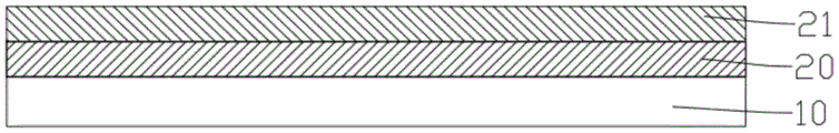
S13, forming a light resistance layer 21 covering the oxide semiconductor layer 20;
specifically, referring to fig. 3, the photoresist layer 21 is coated on the surface of the oxide semiconductor layer 20.
S14, carrying out partition exposure on the oxide semiconductor layer 20, and patterning the photoresist layer 21 to expose two opposite parts of the oxide semiconductor layer 20;
specifically, the photoresist layer 21 is subjected to divisional exposure using a half-tone (halftone) process. Referring to fig. 4, the half-toning plate can include a part of full exposure in addition to the unexposed part and the half-exposed part. This arrangement makes it possible to form three exposure results of the fully exposed region 03, the semi-exposed region 02 and the unexposed region 01 of the photoresist layer 21 in one exposure.
Specifically, the non-exposure region 01 corresponds to a gate 051 portion to be formed on the TFT substrate, the semi-exposure region 02 corresponds to regions of a source 0210, a drain 0211 and a pixel electrode 0212 to be formed on the TFT substrate, and the fully-exposure region 03 corresponds to a region of an insulating layer 031 to be formed on the TFT substrate. The correspondence of positions in this description is the correspondence of the upper and lower structural layers, that is, the correspondence of the projection areas of the structural layers on the substrate 10.
And removing the photoresist layer 21 on the fully exposed region 03 by using a wet etching process, and ashing the residual photoresist layer 21, wherein the photoresist layer 21 is still left on the unexposed region 01 and the semi-exposed region 02, as can be understood from fig. 5, the thickness of the photoresist layer 21 at the unexposed region 01 is thicker than that of the photoresist layer 21 at the semi-exposed region 02, so that in the process of ashing the photoresist layer 21, by setting and controlling the ashing depth, when the oxide semiconductor layer 20 at the semi-exposed region 02 is exposed, a part of the photoresist layer 21 at the unexposed region 01 still remains. At this time, the semi-exposure region 02 is divided into a portion to be formed with the source electrode 0210, a portion to be formed with the drain electrode 0211 and a portion to be formed with the pixel electrode region 0212, and the two portions are relatively independent.
S15, conducting two opposite parts of the oxide semiconductor layer 20, wherein one part forms a source electrode 0210, and the other part forms a drain electrode 0211 and a pixel electrode 0212 electrically connected with the drain electrode 0211;
specifically, the two opposite portions of the exposed oxide semiconductor layer 20 are made into conductors by using helium or argon plasma, and the process conditions include a chamber pressure of 10 to 150mT, a radio frequency energy of 800 to 10000W, and a gas flow of 200 to 4000 sccm. Referring to fig. 6, the oxide semiconductor layer 20 after being made conductive is changed from the initial all-semiconductor state to the "conductor-semiconductor-conductor" state, and the source electrode 0210, the drain electrode 0211 and the pixel electrode 0212 are formed at this time, see fig. 8.
And S16, removing the patterned photoresist layer 21, wherein the oxide semiconductor layer 20 covered by the patterned photoresist layer 21 becomes a channel region 011.
Specifically, the remaining photoresist layer 21 at the oxide semiconductor layer 20 is removed by ashing, and the oxide semiconductor layer 20 includes the conductor 021 and the semiconductor channel region 011 at this time, as shown in fig. 7. The semiconductor exists as the channel region 011 structure of the present TFT substrate. The position of the channel region 011 corresponds to the position of the grid 051, and the function of the TFT substrate is guaranteed to be realized.
According to the manufacturing method of the TFT substrate, the oxide semiconductor layer 20 is subjected to partition exposure, the conductor 021 comprising the source electrode 0210, the drain electrode 0211 and the pixel electrode 0212 and a semiconductor serving as the channel region 011 structure corresponding to the position of the grid 051 are formed at one time, and the space of the insulating layer 031 is formed, so that sub-pixel regions independently exist, and normal functions can be realized. The method can combine the manufacture of the grid 051, the source line 040, the drain line 041 and other structural layers in various forms to reduce a photoetching process and simplify the manufacturing procedure of the traditional plane type oxide semiconductor TFT substrate.
Fig. 9 shows a second embodiment of the method for fabricating a planar oxide semiconductor TFT substrate according to the present invention, which includes the following steps:
s201, providing a substrate 10;
specifically, the substrate 10 may be a transparent substrate, such as glass, plastic, etc.
S202, depositing a buffer layer on the substrate 10;
specifically, the buffer layer may be a silicon oxide buffer layer, which is not shown in the figure. The buffer layer is mainly used for isolating pollutants, bending stress and the like encountered by the planar oxide semiconductor TFT substrate in the subsequent manufacturing process. In some embodiments, the buffer layer may not be required to be disposed under the premise of better control of the process conditions, so as to save the manufacturing time.
S203, depositing the oxide semiconductor layer 20 on the buffer layer;
specifically, referring to fig. 2, the material of the oxide semiconductor layer 20 may be IGZO and may be deposited by physical vapor deposition, and referring to fig. 2, the material of the oxide semiconductor layer 20 may be IGZO and may be deposited by physical vapor deposition.
S204, forming a light resistance layer 21 covering the oxide semiconductor layer 20;
specifically, referring to fig. 3, the photoresist layer 21 is coated on the surface of the oxide semiconductor layer 20.
S205, carrying out partition exposure on the oxide semiconductor layer 20, and patterning the photoresist layer 21 to expose two opposite parts of the oxide semiconductor layer 20;
specifically, the photoresist layer 21 is subjected to divisional exposure using a half-tone (halftone) process. Referring to fig. 4, the half-toning plate can include a part of full exposure in addition to the unexposed part and the half-exposed part. This arrangement makes it possible to form three exposure results of the fully exposed region 03, the semi-exposed region 02 and the unexposed region 01 of the photoresist layer 21 in one exposure.
And removing the photoresist layer 21 on the fully exposed region 03 by using a wet etching process, and ashing the residual photoresist layer 21, wherein the photoresist layer 21 is still left on the unexposed region 01 and the semi-exposed region 02, as can be understood from fig. 5, the thickness of the photoresist layer 21 at the unexposed region 01 is thicker than that of the photoresist layer 21 at the semi-exposed region 02, so that in the process of ashing the photoresist layer 21, by setting and controlling the ashing depth, when the oxide semiconductor layer 20 at the semi-exposed region 02 is exposed, a part of the photoresist layer 21 at the unexposed region 01 still remains. At this time, the semi-exposure region 02 is divided into a portion to be formed with the source electrode 0210 and another portion to be formed with the drain electrode 0211 and the pixel electrode region 0212, and the two portions are relatively independent.
S206, conducting two opposite parts of the oxide semiconductor layer 20, wherein one part forms a source electrode 0210, and the other part forms a drain electrode 0211 and a pixel electrode 0212 electrically connected with the drain electrode 0211;
specifically, the two opposite portions of the exposed oxide semiconductor layer 20 are made into conductors, and helium or argon plasma is usually adopted, wherein the process conditions include a chamber pressure of 10-150 mT, a radio frequency energy of 800-10000W, and a gas flow of 200-4000 sccm. Referring to fig. 6, the oxide semiconductor layer 20 after being made conductive is changed from the initial all-semiconductor state to the "conductor-semiconductor-conductor" state, and the source electrode 0210, the drain electrode 0211 and the pixel electrode 0212 are formed at this time, see fig. 8.
S207, the patterned photoresist layer 21 is removed, and the oxide semiconductor layer 20 covered by the patterned photoresist layer 21 becomes the channel region 011.
Specifically, the remaining photoresist layer 21 at the oxide semiconductor layer 20 is removed by ashing, and the oxide semiconductor layer 20 includes the conductor 021 and the semiconductor channel region 011 at this time, as shown in fig. 7. The semiconductor exists as the channel region 011 structure of the present TFT substrate. The position of the channel region 011 corresponds to the position of the grid 051, and the function of the TFT substrate is guaranteed to be realized.
S208, depositing an insulating layer 031;
specifically, referring to fig. 10, the insulating layer 031 needs to completely cover the entire extent of the sub-pixel region.
S209, patterning the insulating layer 031 to form two connection holes 04 on the insulating layer 031, so that the two connection holes penetrate through the insulating layer 031 to expose the source 0210 and the drain 0211;
specifically, the pattern of the connection hole 04 is defined by photolithography, and here, the photomask is used for the second time in the manufacturing method of the TFT substrate of the present invention. Referring to fig. 11 and 12, a dry etching process is used to etch the shape of the connection hole 04 on the insulating layer 031, that is, the material of the insulating layer 031 in the pattern of the connection hole 04 is removed, so that the conductor 021, that is, the source 0210 and the drain 0211, at the lower portion of the insulating layer 031 are exposed, one of the connection holes 04 is communicated with the source 0210, and the other connection hole 04 is communicated with the drain 0211.
S210, depositing a metal layer 05;
specifically, a layer of the metal layer 05 is deposited on the insulating layer 031, and the connection hole 04 needs to be filled with the metal layer 05 to connect the conductor 021 to the metal layer 05, as shown in fig. 13. It is understood that the metal layer 05 is connected to the source 0210 and drain 0211 portions of the conductor 021.
S211, patterning the metal layer 05 to form a grid 051, a grid line 052, a source line 040 and a drain line 041, wherein the grid 051 is electrically connected with the grid line 052, the grid 051 is arranged corresponding to the channel region 011, the source line 040 is connected with the source electrode 0210 through the connecting hole 04, the drain line 041 is connected with the drain electrode 0211 through the other connecting hole 04, the source line 040 is arranged at intervals with the grid 051 and the grid line 052, and the drain line 041 is arranged at intervals with the grid 051 and the grid line 052;
specifically, the gate lines 051, the gate lines 052, the source lines 040, and the drain lines 041 are patterned on the metal layer 05 by photolithography. Specifically, referring to fig. 14 and 15, the gate 051, the gate line 052, the source line 040 and the drain line 041 are etched and formed by a wet etching process using a defined pattern. Here, the third photomask is used in the method for manufacturing a TFT substrate of the present invention.
The gate 051 is arranged corresponding to the channel region 011, the source line 040 is connected with the source electrode 0210 through the connecting hole 04, the drain line 041 is connected with the drain electrode 0211 through the other connecting hole 04, the source line 040 is arranged at intervals with the gate 051 and the gate line 052, and the drain line 041 is arranged at intervals with the gate 051 and the gate line 052.
S212, depositing a protective layer 06.
Specifically, referring to fig. 16, after all the structural layers are completely prepared, a protective layer 06 is deposited thereon to protect the TFT substrate of the present invention. It will be appreciated that in some embodiments, the protective layer 06 may not be deposited, and the function of the TFT substrate may be achieved as well.
A third embodiment of the method for manufacturing a planar oxide semiconductor TFT substrate according to the present invention, with reference to fig. 17, includes the following steps:
s301, providing a substrate 10;
specifically, the substrate 10 may be a transparent substrate, such as glass, plastic, etc.
S302, depositing a metal layer 05 on the substrate 10;
specifically, the metal layer 05 is deposited directly on the substrate 10.
S303, patterning the metal layer 05, and defining and forming a grid 051, a grid line 052, a source line 040 and the drain line 041;
specifically, the gate 051, the gate lines 052, the source lines 040 and the drain lines 041 are patterned by a photolithography and/or wet etching process. It is understood that the mask is used for the first time in this embodiment.
S304, depositing an insulating layer 031;
specifically, the insulating layer 031 is deposited over the gate electrode 051, the gate line 052, and the source and drain lines 040, 041.
S305, patterning the insulating layer 031 to define two connection holes 04, where the connection holes 04 penetrate through the insulating layer 031 and respectively communicate with the source line 040 and the drain line 041.
The insulating layer 031 is patterned to define and form a pattern of connection holes 04. It is understood that the connection hole 04 corresponds to the source line 040 and the drain line 041. It is understood that the mask is used for the second time in this embodiment. Specifically, by using a dry etching process, the shape of the connection hole 04 is etched on the insulating layer 031, that is, the material of the insulating layer 031 in the pattern of the connection hole 04 is removed, so that the source line 040 and the drain line 041 under the insulating layer 031 are exposed.
S306, depositing an oxide semiconductor layer 20 on the insulating layer 031;
specifically, the material of the oxide semiconductor layer 20 may be IGZO, and the deposition manner thereof may be physical vapor deposition. As can be understood, the oxide semiconductor layer 20 fills the connection hole 40 during deposition, and connects the source line 040 and the drain line 041.
S307, forming a light resistance layer 21 covering the oxide semiconductor layer 20;
specifically, the photoresist layer 21 is coated on the surface of the oxide semiconductor layer 20.
S308, carrying out partition exposure on the oxide semiconductor layer 20, carrying out no exposure in the region corresponding to the grid 051, carrying out half exposure in the source line 040, the drain line 0211 and the pixel electrode 0212, and carrying out full exposure in the rest regions;
specifically, the photoresist layer 21 is subjected to divisional exposure using a half-tone (halftone) process. The half-toning plate comprises a part of half-exposure part besides a full-exposure part and a non-exposure part, and three exposure results of a full-exposure area 03, a half-exposure area 02 and a non-exposure area 01 of the photoresist layer 21 can be formed in one exposure process.
Specifically, the position of the non-exposure region 01 corresponds to the gate 051 portion of the present embodiment, the position of the semi-exposure region 02 corresponds to the regions of the source 0210, the drain 0211 and the pixel electrode 0212 of the present embodiment, and the position of the fully-exposure region 03 corresponds to the insulating layer 031 region of the present embodiment. It is understood that the correspondence of positions in this description is the correspondence of the upper and lower structural layers, that is, the correspondence of the projection areas of the structural layers on the substrate 10.
It is understood that the photomask is used for the third time in this embodiment.
Specifically, the photoresist layer 21 on the fully exposed region 03 is removed by a wet etching process.
Specifically, the photoresist layer 21 is ashed, and at this time, the photoresist layer 21 remains on the unexposed region 01 and the semi-exposed region 02, and it can be understood that the thickness of the photoresist layer 21 at the unexposed region 01 is thicker than the thickness of the photoresist layer 21 at the semi-exposed region 02, so that in the process of ashing the photoresist layer 21, by setting and controlling the ashing depth, when the oxide semiconductor layer 20 at the semi-exposed region 02 is exposed, a part of the photoresist layer 21 at the unexposed region 01 remains.
S309, processing the semi-exposure area 02 into a conductor 021 by using plasma through a conductor process to form the source electrode 0210, the drain electrode 0211 and the pixel electrode 0212;
specifically, the exposed oxide semiconductor layer 20 is made into a conductor by using helium gas or argon gas plasma, and the process conditions include a chamber pressure of 10 to 150mT, a radio frequency energy of 800 to 10000W, and a gas flow of 200 to 4000 sccm. The oxide semiconductor layer 20 after being made conductive is changed from the initial all-semiconductor state to the "conductor-semiconductor-conductor" state, and the source electrode 0210, the drain electrode 0211, and the pixel electrode 0212 are formed at this time. When the two opposite portions of the oxide semiconductor layer are made conductive, the source electrode 0210 is connected to the source line 040, the drain electrode 0211 is connected to the drain line 041, and the channel region, i.e., the semiconductor 011, is disposed corresponding to the gate 051.
S310, removing the residual photoresist layer 21 of the part 01 of the unexposed area;
specifically, the photoresist layer 21 remaining on the oxide semiconductor layer 20 is removed by ashing, and the oxide semiconductor layer 20 includes the conductor 021 and a semiconductor. The semiconductor exists as a channel region 011 structure of the present TFT substrate, see fig. 18. The position of the channel region 011 corresponds to the position of the grid 051, and the function of the TFT substrate is guaranteed to be realized.
S311, depositing a protective layer 60.
Specifically, referring to fig. 19, after all the structural layers are completely prepared, a protective layer 06 is deposited thereon to protect the planar oxide semiconductor TFT substrate. It will be appreciated that in some embodiments, the protective layer 06 may not be deposited, and the function of the TFT substrate may be achieved as well.
According to the manufacturing method of the TFT substrate, semiconductors are sequentially formed on the oxide semiconductor layer corresponding to the grid electrodes through a partition exposure process method, conductors are formed in the areas corresponding to the source electrodes, the drain electrodes and the pixel electrodes, and the rest parts are removed through wet etching and correspond to the positions of the insulation areas. Compared with the manufacturing method in the prior art, the TFT substrate which needs to be molded by four photoetching procedures is compressed into three photoetching procedures for molding, so that one photoetching procedure flow is omitted, the process is simplified, and the production efficiency is improved.
The above-described embodiments do not limit the scope of the present invention. Any modification, equivalent replacement, and improvement made within the spirit and principle of the above-described embodiments should be included in the protection scope of the technical solution.
Claims (9)
1. A manufacturing method of a TFT substrate is characterized by comprising the following steps:
providing a substrate;
depositing a metal layer on the substrate;
patterning the metal layer to form a gate electrode, a gate line, a source line and a drain line;
depositing an insulating layer;
patterning the insulating layer, defining two connecting holes, wherein the connecting holes penetrate through the insulating layer and are respectively communicated with the source line and the drain line;
depositing an oxide semiconductor layer on the insulating layer;
forming a photoresist layer covering the oxide semiconductor layer;
exposing in a subarea mode to pattern the photoresist layer so as to expose two opposite parts of the oxide semiconductor layer;
conducting two opposite parts of the oxide semiconductor layer, wherein one part forms a source electrode, the other part forms a drain electrode and a pixel electrode electrically connected with the drain electrode, the source electrode is communicated with the source electrode line, and the drain electrode is communicated with the drain electrode line;
and removing the residual patterned photoresist layer, and forming a channel region corresponding to the gate by the oxide semiconductor layer covered by the residual patterned photoresist layer.
2. The method of fabricating the TFT substrate of claim 1, wherein the oxide semiconductor layer is deposited on the substrate, and further comprising, after forming the channel region, the steps of:
depositing an insulating layer;
patterning the insulating layer to form two connecting holes on the insulating layer, wherein the two connecting holes penetrate through the insulating layer to expose the source electrode and the drain electrode;
depositing a metal layer;
patterning the metal layer to form a gate electrode, a gate line, a source line and a drain line, the gate electrode being electrically connected to the gate line, the gate electrode being disposed corresponding to the channel region, the source line being connected to the source electrode through the connection hole, the drain line being connected to the drain electrode through another connection hole, the source line being spaced apart from the gate electrode and the gate line, and the drain line being spaced apart from the gate electrode and the gate line.
3. The method of manufacturing the TFT substrate according to claim 2, further comprising, before depositing the oxide semiconductor layer on the substrate, the steps of:
depositing a buffer layer on the substrate.
4. The method for manufacturing the TFT substrate according to claim 1, wherein the connection hole is filled with the oxide semiconductor layer when the oxide semiconductor layer is deposited.
5. The method for manufacturing a TFT substrate according to claim 1, wherein the act of depositing the oxide semiconductor layer is performed by a physical vapor deposition method.
6. The method of manufacturing the TFT substrate according to claim 1, wherein the oxide semiconductor layer is formed of IGZO.
7. The method for manufacturing a TFT substrate according to claim 1, wherein the step of exposing the oxide semiconductor layer in divided regions is performed by a halftone process.
8. The method of manufacturing a TFT substrate according to claim 1, wherein a helium gas or an argon gas plasma is used for conducting the oxide semiconductor layer.
9. The method of fabricating a TFT substrate according to any one of claims 1 to 8, wherein a protective layer is deposited after the channel region is formed.
Priority Applications (2)
| Application Number | Priority Date | Filing Date | Title |
|---|---|---|---|
| CN201711124844.7A CN107910351B (en) | 2017-11-14 | 2017-11-14 | Manufacturing method of TFT substrate |
| PCT/CN2018/074991 WO2019095562A1 (en) | 2017-11-14 | 2018-02-01 | Method for manufacturing tft substrate |
Applications Claiming Priority (1)
| Application Number | Priority Date | Filing Date | Title |
|---|---|---|---|
| CN201711124844.7A CN107910351B (en) | 2017-11-14 | 2017-11-14 | Manufacturing method of TFT substrate |
Publications (2)
| Publication Number | Publication Date |
|---|---|
| CN107910351A CN107910351A (en) | 2018-04-13 |
| CN107910351B true CN107910351B (en) | 2020-06-05 |
Family
ID=61844178
Family Applications (1)
| Application Number | Title | Priority Date | Filing Date |
|---|---|---|---|
| CN201711124844.7A Active CN107910351B (en) | 2017-11-14 | 2017-11-14 | Manufacturing method of TFT substrate |
Country Status (2)
| Country | Link |
|---|---|
| CN (1) | CN107910351B (en) |
| WO (1) | WO2019095562A1 (en) |
Families Citing this family (3)
| Publication number | Priority date | Publication date | Assignee | Title |
|---|---|---|---|---|
| CN109994530B (en) | 2019-03-28 | 2021-01-26 | 云谷(固安)科技有限公司 | Display device, display panel and manufacturing method thereof |
| CN110718467B (en) * | 2019-09-24 | 2021-12-03 | Tcl华星光电技术有限公司 | Manufacturing method of TFT array substrate |
| CN111180471A (en) * | 2020-03-02 | 2020-05-19 | 南京中电熊猫平板显示科技有限公司 | Array substrate and manufacturing method thereof |
Citations (7)
| Publication number | Priority date | Publication date | Assignee | Title |
|---|---|---|---|---|
| JP2007103418A (en) * | 2005-09-30 | 2007-04-19 | Seiko Epson Corp | Semiconductor device, method for manufacturing semiconductor device, and electro-optical device |
| CN101577283A (en) * | 2008-05-06 | 2009-11-11 | 三星移动显示器株式会社 | Thin film transistor array arrangement, organic light emitting display device having the same, and manufacturing method thereof |
| CN101825815A (en) * | 2009-03-06 | 2010-09-08 | 北京京东方光电科技有限公司 | TFT (Thin Film Transistor)-LCD (Liquid Crystal Display) array baseplate and manufacturing method thereof |
| CN102890378A (en) * | 2012-09-17 | 2013-01-23 | 京东方科技集团股份有限公司 | Array substrate and fabrication method of array substrate |
| CN104681627A (en) * | 2015-03-10 | 2015-06-03 | 京东方科技集团股份有限公司 | Array substrate, thin-film transistor and manufacturing methods thereof as well as display device |
| CN105118777A (en) * | 2015-07-01 | 2015-12-02 | 深圳市华星光电技术有限公司 | Manufacturing method for TFT back board and structure |
| CN106384714A (en) * | 2016-10-13 | 2017-02-08 | 京东方科技集团股份有限公司 | Thin film transistor, manufacturing method thereof, and array substrate |
Family Cites Families (4)
| Publication number | Priority date | Publication date | Assignee | Title |
|---|---|---|---|---|
| CN102023424B (en) * | 2009-09-09 | 2013-04-03 | 北京京东方光电科技有限公司 | TFT-LCD array substrate and manufacture method thereof |
| US20130320335A1 (en) * | 2012-06-01 | 2013-12-05 | Semiconductor Energy Laboratory Co., Ltd. | Semiconductor device and method for manufacturing the same |
| CN103715094B (en) * | 2013-12-27 | 2017-02-01 | 京东方科技集团股份有限公司 | Thin film thyristor and manufacturing method thereof, array substrate and manufacturing method thereof and display device |
| CN104393051A (en) * | 2014-10-31 | 2015-03-04 | 京东方科技集团股份有限公司 | Thin film transistor and preparation method thereof and array substrate |
-
2017
- 2017-11-14 CN CN201711124844.7A patent/CN107910351B/en active Active
-
2018
- 2018-02-01 WO PCT/CN2018/074991 patent/WO2019095562A1/en not_active Ceased
Patent Citations (7)
| Publication number | Priority date | Publication date | Assignee | Title |
|---|---|---|---|---|
| JP2007103418A (en) * | 2005-09-30 | 2007-04-19 | Seiko Epson Corp | Semiconductor device, method for manufacturing semiconductor device, and electro-optical device |
| CN101577283A (en) * | 2008-05-06 | 2009-11-11 | 三星移动显示器株式会社 | Thin film transistor array arrangement, organic light emitting display device having the same, and manufacturing method thereof |
| CN101825815A (en) * | 2009-03-06 | 2010-09-08 | 北京京东方光电科技有限公司 | TFT (Thin Film Transistor)-LCD (Liquid Crystal Display) array baseplate and manufacturing method thereof |
| CN102890378A (en) * | 2012-09-17 | 2013-01-23 | 京东方科技集团股份有限公司 | Array substrate and fabrication method of array substrate |
| CN104681627A (en) * | 2015-03-10 | 2015-06-03 | 京东方科技集团股份有限公司 | Array substrate, thin-film transistor and manufacturing methods thereof as well as display device |
| CN105118777A (en) * | 2015-07-01 | 2015-12-02 | 深圳市华星光电技术有限公司 | Manufacturing method for TFT back board and structure |
| CN106384714A (en) * | 2016-10-13 | 2017-02-08 | 京东方科技集团股份有限公司 | Thin film transistor, manufacturing method thereof, and array substrate |
Also Published As
| Publication number | Publication date |
|---|---|
| CN107910351A (en) | 2018-04-13 |
| WO2019095562A1 (en) | 2019-05-23 |
Similar Documents
| Publication | Publication Date | Title |
|---|---|---|
| CN109671726B (en) | Array substrate and manufacturing method thereof, display panel, and display device | |
| CN109300840B (en) | Display substrate, manufacturing method thereof and display device | |
| US10236388B2 (en) | Dual gate oxide thin-film transistor and manufacturing method for the same | |
| WO2017173712A1 (en) | Thin-film transistor, production method thereof, array substrate and display device | |
| US20170186879A1 (en) | Thin Film Transistor, Array Substrate and Manufacturing Processes of Them | |
| CN103681514B (en) | Array base palte and preparation method thereof, display unit | |
| CN107910351B (en) | Manufacturing method of TFT substrate | |
| CN103117224A (en) | Manufacturing method of thin film transistor and array substrate | |
| WO2020228499A1 (en) | Transistor device and manufacturing method therefor, display substrate and display apparatus | |
| CN109037241B (en) | LTPS array substrate, manufacturing method thereof, and display panel | |
| CN105629598B (en) | The array substrate and production method of FFS mode | |
| CN108231553A (en) | The production method of thin film transistor (TFT) and the production method of array substrate | |
| WO2021031374A1 (en) | Preparation method for array substrate and array substrate | |
| US20210175309A1 (en) | Active device substrate and manufacturing method thereof | |
| WO2019210602A1 (en) | Array substrate, manufacturing method therefor and display panel | |
| CN105529274A (en) | Manufacturing method of thin-film transistor, array substrate and display device | |
| CN113889489B (en) | Array substrate and preparation method thereof, and display device | |
| CN109037243B (en) | Substrate for display device, manufacturing method of substrate and display device | |
| CN110718467B (en) | Manufacturing method of TFT array substrate | |
| CN102709329A (en) | Thin film transistor and manufacturing method thereof | |
| CN105931985A (en) | Array substrate, preparation method therefor, and display device | |
| CN101197332A (en) | How to make pixel structure | |
| CN104112711A (en) | Manufacturing method of coplanar oxide semiconductor TFT (Thin Film Transistor) substrate | |
| CN101409262A (en) | Pixel structure and manufacturing method thereof | |
| CN110993619B (en) | Array substrate, preparation method thereof and display device |
Legal Events
| Date | Code | Title | Description |
|---|---|---|---|
| PB01 | Publication | ||
| PB01 | Publication | ||
| SE01 | Entry into force of request for substantive examination | ||
| SE01 | Entry into force of request for substantive examination | ||
| GR01 | Patent grant | ||
| GR01 | Patent grant | ||
| CP01 | Change in the name or title of a patent holder |
Address after: 9-2 Tangming Avenue, Guangming New District, Shenzhen City, Guangdong Province Patentee after: TCL China Star Optoelectronics Technology Co.,Ltd. Address before: 9-2 Tangming Avenue, Guangming New District, Shenzhen City, Guangdong Province Patentee before: Shenzhen China Star Optoelectronics Technology Co.,Ltd. |
|
| CP01 | Change in the name or title of a patent holder |