Detailed Description
The following disclosure provides many different embodiments, or examples, for implementing different features of the provided subject matter. Specific examples of components and arrangements are described below to simplify the present disclosure. These are, of course, merely examples and are not intended to limit the invention. For example, in the following description, forming a first feature over or on a second feature may include embodiments in which the first and second features are formed in direct contact, and may also include embodiments in which additional features may be formed between the first and second features, such that the first and second features may not be in direct contact. Moreover, the present disclosure may repeat reference numerals and/or letters in the various examples. This repetition is for the purpose of simplicity and clarity and does not in itself dictate a relationship between the various embodiments and/or configurations discussed.
Also, spatially relative terms such as "below …," "below …," "lower," "above …," "upper," and the like may be used herein for ease of description to describe one element or component's relationship to another (or other) elements or components as illustrated. Spatially relative terms are intended to encompass different orientations of the device in use or operation in addition to the orientation depicted in the figures. The device may be otherwise oriented (rotated 90 degrees or at other orientations) and the spatially relative descriptors used herein interpreted accordingly. Throughout the specification, "substantially" is used to explain a deviation in data accuracy caused by, for example, limitations of respective manufacturing processes.
Various embodiments provide one or more of the following non-limiting benefits: source/drain epitaxial facet improvement; cutting and patterning the pseudo active region; improved source/drain contact opening bonding process window, less short channel effects; less source/drain contact etch process loading requirements; improved reliability; reduced leakage current; and improved yield.
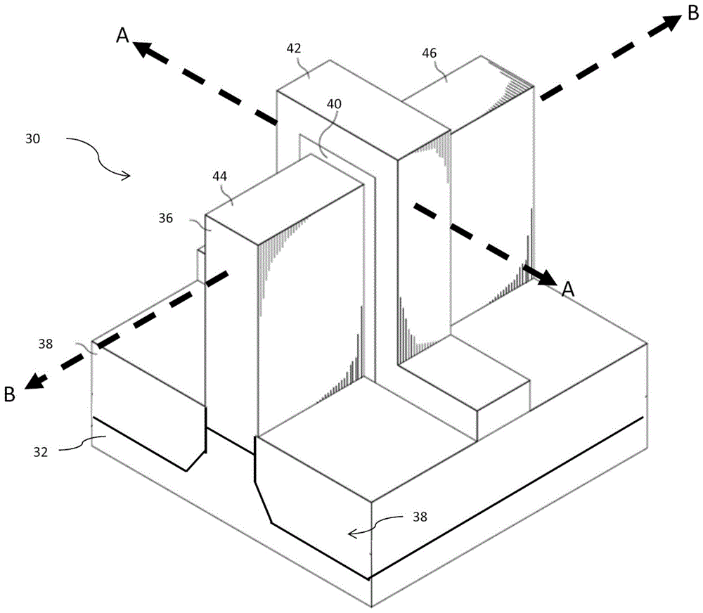
Fig. 1 shows an example of a fin field effect transistor (FinFET)30 in a three-dimensional view. FinFET 30 includes a semiconductor fin 36 on a semiconductor substrate 32. Substrate 32 includes isolation regions 38, and fins 36 protrude above adjacent isolation regions 38 and are formed between adjacent isolation regions 38. A gate dielectric 40 is along the sidewalls of fin 36 and over the top surface of fin 36, and a gate electrode 42 is over gate dielectric 40. The gate dielectric 40 and the gate electrode 42 constitute a gate stack in the finFET 30. The portion of the fin 36 covered by the gate dielectric 40/gate electrode 42 may be referred to as a channel region of the finFET 30. Source/ drain regions 44 and 46 are disposed in opposite sides of fin 36 relative to gate dielectric 40 and gate electrode 42. The cross-section a-a passes through the channel, gate dielectric 40 and gate electrode 42 of the finFET 30. Cross section B-B is perpendicular to cross section a-a and along the longitudinal axis of fin 36 and in the direction of current flow, for example, between source/ drain regions 44 and 46. For clarity, the subsequent figures refer to these reference sections.
Fig. 2, 3A, 3B, 4, 5A, 5B, 6, 7A, 7B, 8A, 8B, 9A, 9B, 10A, 10B, 11A, 11B, 12, 13A, 13B, 14A, 14B, 15A, 15B, 15C, 16A, 16B, 17A, 17B, 18A, 18B, 19A, and 19B are cross-sectional and top views of an intermediate stage in fabrication according to one exemplary embodiment. Fig. 2 shows the reference cross-section a-a shown in fig. 1, except for a plurality of finfets. In fig. 3A, 3B, 5A, 5B, 7A, 7B, 8A, 8B, 9A, 9B, 10A, 10B, 11A, 11B, 12, 13A, 13B, 15A, 15B, 16A, 16B, 17A, 17B, 18A, 18B, 19A, and 19B, the diagram ending with the "a" symbol is shown along a similar section a-a; the figures ending with the "B" symbol are shown along a similar section B-B; fig. 4, 6, 14A, and 14B illustrate top-down views of multiple finfets according to an example embodiment. Fig. 15C shows a cross-sectional view of the device taken along a similar section B-B.
Fig. 2 shows a substrate 50. The substrate 50 may be a doped (e.g., doped with p-type or n-type dopants) or undoped semiconductor substrate, such as a bulk semiconductor, a semiconductor-on-insulator (SOI) substrate, or the like. Substrate 50 may be a wafer, such as a silicon wafer. Generally, an SOI substrate includes a layer of semiconductor material formed on an insulating layer. For example, the insulating layer may be a Buried Oxide (BOX) layer, a silicon oxide layer, or the like. An insulating layer is provided on a substrate, typically a silicon substrate or a glass substrate. Other substrates such as multilayer or gradient substrates may also be used. In some embodiments, the semiconductor material of substrate 50 may include silicon; germanium; a compound semiconductor including silicon carbide, gallium arsenide, gallium phosphide, indium arsenide, and/or indium antimonide; an alloy semiconductor including SiGe, GaAsP, AlInAs, AlGaAs, GaInAs, GaInP, and/or GaInAsP; or a combination thereof.
The substrate 50 has a first region 50A and a second region 50B. The first region 50A may be used to form an n-type device such as an NMOS transistor (such as an n-type FinFET). The second region 50B may be used to form a p-type device such as a PMOS transistor (such as a p-type FinFET). Although fig. 2 shows the first region 50A and the second region 50B as being contiguous, any number of components (e.g., other active devices, isolation regions, passive devices, etc.) may be disposed between the first region 50A and the second region 50B depending on the device design.
As further illustrated by fig. 2, a hard mask 53 may be disposed over the substrate 50. The hard mask may include one or more oxide (e.g., silicon oxide layer 53A) and/or nitride (e.g., silicon nitride layer 53B) layers to reduce damage to the underlying substrate 50 during patterning in subsequent process steps. The hard mask 53 may be formed using any suitable deposition process such as Atomic Layer Deposition (ALD), Chemical Vapor Deposition (CVD), high density plasma CVD (HDP-CVD), Physical Vapor Deposition (PVD), and the like.
Fig. 3A, 3B, 4, 5A, 5B, 6, 7A, and 7B illustrate patterning of the substrate 50 to form semiconductor fins 52 (see fig. 7A and 7B) and to define trenches 55A and 55B (see fig. 7A and 7B) between the semiconductor fins 52, the trenches 55A and 55B for subsequently forming isolation regions. In an embodiment, patterning the substrate 50 includes a combination of lithography and etching. Patterning substrate 50 may include multiple photolithography and etching steps. For example, referring first to fig. 3A and 3B, after forming the hard mask 53, a photoresist material may be blanket deposited over the hard mask 53. The photoresist material can then be patterned by exposing the photoresist material to light using a photomask. Either the exposed or unexposed portions of the photoresist can then be removed depending on whether a positive or negative photoresist is used. The resulting patterned photoresist material is shown in fig. 3A and 3B as first photoresist 57. Then, the pattern of the first photoresist 57 may be transferred to the hard mask 53 using an etching process to define the trench 55A in the hard mask 53. The pattern of the first photoresist 57 may define a trench 55A in the section a-a (see fig. 3A) and not define any trench in the section B-B (see fig. 3B).
For example, fig. 4 shows a top down view of the hard mask 53 after the pattern of the first photoresist 57 has been transferred to the hard mask 53. In FIG. 4, the cross-sectional view provided by FIG. 3A is taken along dashed line 3A-3A and the cross-sectional view provided by FIG. 3B is taken along dashed line 3B-3B. As shown by fig. 4, the length of the trench 55A may extend in the x-direction, which may be substantially parallel to the section B-B of fig. 3B. The width W1 of the trench 55A may extend in the y-direction, which may be substantially parallel to the section a-a of fig. 3A. In some embodiments, the width W1 of each trench 55A in the y-direction may be about 10nm to about 1 μm. In other embodiments, the width W1 may be a different size.
For example, after the pattern of the first photoresist 57 is transferred to the hard mask 53, the first photoresist 57 is removed in an ashing and/or wet stripping process. Subsequently, in fig. 5A and 5B, a second photoresist 59 is formed and patterned over the hard mask 53. For example, a photoresist material may be blanket deposited over the hard mask 53. The blanket deposition process may be a non-conformal process and a photoresist material may be deposited to fill the trench 55A (see fig. 5A). The photoresist material can then be patterned by exposing the photoresist material to light using a photomask. Then, depending on whether a positive or negative photoresist is used, either the exposed or unexposed portions of the photoresist may be removed. The resulting patterned photoresist material is shown in fig. 5A and 5B as second photoresist 59. Then, an etching process may be used to cause the pattern of the second photoresist 59 to be transferred to the hard mask 53 to define the trench 55B in the hard mask 53. The pattern of second photoresist 59 may define trench 55B in section B-B (see fig. 5B) without defining any additional trenches in section a-a (see fig. 5A).
For example, fig. 6 shows a top down view of the hard mask 53 after the pattern of the second photoresist 59 has been transferred to the hard mask 53. In FIG. 6, the cross-sectional view provided by FIG. 5A is taken along dashed line 5A-5A and the cross-sectional view provided by FIG. 5B is taken along dashed line 5B-5B. As shown by fig. 6, the length of the trench 55B may extend in the y-direction, which may be substantially parallel to the section a-a of fig. 5A. The length of the trench 55B may also be substantially perpendicular to the length of the trench 55A. The width W2 of the trench 55B may extend in the x-direction, which may be substantially parallel to the section B-B of fig. 3B. In some embodiments, a width W2 of each trench 55B in the x-direction may be less than a width W1 of each trench 55A in the y-direction. For example, the width W2 may be about 2nm to about 30 nm. In other embodiments, the width W1 may be a different size. Width W2 is still further smaller than the respective widths (e.g., in the x-direction) of subsequently formed dummy gate structures (e.g., dummy gate 70, see fig. 11B). For example, after the pattern of the second photoresist 59 is transferred to the hard mask 53, the second photoresist 59 is removed in an ashing and/or wet stripping process.
Subsequently, during an etching process as illustrated by fig. 7A and 7B, trenches 55A and 55B are patterned into the underlying substrate 50 using the hard mask 53 as a patterning mask. The etching of the substrate 50 may include an acceptable etching process such as Reactive Ion Etching (RIE), Neutral Beam Etching (NBE), the like, or combinations thereof. The etching may be anisotropic. The photoresist is then removed, for example, in an ashing and/or wet strip process. Thus, the fin 52 is formed. The fins 52 extend upwardly from the base substrate 50 between adjacent trenches 55A/55B. As described above, fig. 7A and 7B show vertical sections. Thus, the length of trenches 55A and 55B may also be substantially perpendicular. Additionally, the width W1 of trench 55A (e.g., between adjacent fins 52 in cross-section a-a) may be greater than the width W2 of trench 55B (e.g., between adjacent fins 52 in cross-section B-B). The difference in width may be achieved, at least in part, by a multi-step lithographic process as described above.
In an embodiment, the fin 52 extends above the substrate 50 to a height H1 of about 5nm to about 200 nm. In an embodiment, each fin 52 may be long enough to allow for the formation of multiple dummy gate stacks on each fin 52 in subsequent process steps. For example, a Critical Dimension (CD) L1 of each fin 52 in cross-section B-B (see fig. 1) may be about 5nm to about 20nm, where CD L1 is measured from a first sidewall of a fin 52 to a corresponding first sidewall of an adjacent fin 52. In other embodiments, the fins 52 may have different dimensions.
In fig. 8A and 8B, an insulating material is formed between adjacent fins 52 to form isolation regions 54 in trenches 55A and 55B (see fig. 3A and 3B). The insulating material of isolation region 54 may be an oxide, such as silicon oxide, nitride, or the like, or combinations thereof, and may be formed by high density plasma chemical vapor deposition (HDP-CVD), flowable CVD (fcvd) (e.g., CVD based material deposition in a remote plasma system and post-cure to convert it to another material, such as an oxide), or the like, or combinations thereof. Other insulating materials formed by any acceptable process may be used. Once the insulating material is formed, an annealing process may be performed. In the illustrated embodiment, the isolation regions 54 comprise silicon oxide formed by an FCVD process. In some embodiments, isolation regions 54 may be formed to fill trenches 55A and 55B (see fig. 7A and 7B) and cover the top surface of fin 52. Subsequently, a planarization process such as Chemical Mechanical Polishing (CMP) may remove any excess insulating material and form the top surfaces of coplanar isolation regions 54 and the top surfaces of fins 52. The planarization process may also remove the mask 53 from the top surface of the fin 52 (see fig. 7A and 7B). In other embodiments, the mask 53 may be removed using a separate process rather than planarization.
Additionally, in some embodiments, isolation region 54 may include a conformal liner (not shown) formed on the sidewalls and bottom surfaces of trenches 55A and 55B (see fig. 7A and 7B) prior to filling trenches 55A and 55B with the insulating material of isolation region 54. In some embodiments, the liner may comprise a semiconductor (e.g., silicon) nitride, a semiconductor (e.g., silicon) oxide, a thermal semiconductor (e.g., silicon) oxide, a semiconductor (e.g., silicon) oxynitride, a polymer dielectric, combinations thereof, and the like. The liner formation may include any suitable method, such as ALD, CVD, High Density Plasma (HDP) CVD, PVD, and the like. In such embodiments, the liner may prevent (or at least reduce) diffusion of semiconductor material from the fin 52 (e.g., Si and/or Ge) into the surrounding isolation region 54 during annealing of the isolation region 54.
Fig. 9A and 9B illustrate the recessing of the
isolation regions 54 to form Shallow Trench Isolation (STI)
regions 54. The
isolation regions 54 are recessed such that the
fins 56 in the
first region 50A and in the
second region 50B protrude from between
adjacent isolation regions 54 along a section a-a (see fig. 1) as shown by fig. 9A. However, at least a portion of the
isolation region 54 between
adjacent fins 52/56 may not be recessed along section B-B (see fig. 1) as shown by 9B. Further, the top surface of the
isolation region 54 may have a planar surface as shown, a convex surface, a concave surface (such as recessed), or a combination thereof. The top surface of
isolation region 54 may be formed flat, convex, and/or concave by appropriate etching. The
isolation regions 54 may be recessed using an acceptable etch process, such as an etch process that is selective to the material of the
isolation regions 54. For example, the use of
Etching or chemical oxide removal using a material SICONI tool or dilute hydrofluoric acid (dHF). The masking layer may be formed to selectively etch
isolation regions 54 in
trenches 55A (see fig. 7A) without etching at least portions of
isolation regions 54 in
trenches 55B (see fig. 7B).
Those of ordinary skill in the art will readily appreciate that the process described with respect to fig. 2-9B is but one example of how the fin 56 may be formed. In other embodiments, a dielectric layer may be formed over the top surface of the substrate 50; a trench may be etched through the dielectric layer; a homoepitaxial structure can be epitaxially grown in the trench; and the dielectric layer may be recessed such that the homoepitaxial structure protrudes from the dielectric layer to form a fin. In still other embodiments, a heteroepitaxial structure may be used for the fins. For example, the semiconductor strips 52 in fig. 7A and 7B may be recessed, and materials other than the semiconductor strips 52 may be epitaxially grown in their locations. In still further embodiments, a dielectric layer may be formed over the top surface of the substrate 50; a trench may be etched through the dielectric layer; a heteroepitaxial structure may be epitaxially grown in the trench using a material different from the substrate 50; and isThe dielectric layer may be recessed such that the hetero-epitaxial structure protrudes from the dielectric layer to form fin 56. In some embodiments in which a homoepitaxial or heteroepitaxial structure is epitaxially grown, the grown material may be doped in situ during growth, which may avoid both prior and subsequent implantations, although both in situ and implant doping may be used. Furthermore, it may be advantageous to epitaxially grow a material in the NMOS region that is different from the material in the PMOS region. In various embodiments, fin 56 may comprise silicon germanium (Si)xGe1-xWhere x may be between about 0 and 100), silicon carbide, pure or substantially pure germanium, group III-V compound semiconductors, group II-VI compound semiconductors, and the like. For example, usable materials for forming group III-V compound semiconductors include, but are not limited to, InAs, AlAs, GaAs, InP, GaN, InGaAs, InAlAs, GaSb, AlSb, AlP, GaP, and the like.
In fig. 9A and 9B, appropriate wells may be formed in fin 56, fin 52, and/or substrate 50. For example, a P-well may be formed in the first region 50A, and an N-well may be formed in the second region 50B.
Different implantation steps for the different regions 50A and 50B may be achieved using a photoresist or other mask (not shown). For example, a photoresist is formed over fin 56 and isolation region 54 in first region 50A. The photoresist is patterned to expose a second region 50B of the substrate 50, such as a PMOS region. The photoresist may be formed by using spin-on techniques and may be patterned using acceptable photolithography techniques. Once the photoresist is patterned, n-type impurity implantation is performed in the second region 50B, and the photoresist may act as a mask to substantially prevent n-type impurities from being implanted into the first region 50A, such as an NMOS region. In the first zone to 10 or less18cm-3Such as at a concentration of from about 1017cm-3To about 1018cm-3Within the range of (1) may be phosphorus, arsenic, or the like. After implantation, the photoresist is removed, for example, by an acceptable ashing process.
After implantation of second region 50B, a photoresist is formed over fin 56 and isolation region 54 in second region 50B. The photoresist is patterned to expose a first region 50A of the substrate 50, such as an NMOS region. Can be formed by using spin coating techniqueA photoresist is formed and the photoresist can be patterned using acceptable photolithography techniques. Once the photoresist is patterned, a p-type impurity implant may be performed in the first region 50A, and the photoresist may act as a mask to substantially prevent the p-type impurity from being implanted into the second region, such as the PMOS region. In the first zone to 10 or less18cm-3Such as at a concentration of from about 1017cm-3To about 1018cm-3In the range of (1) may be boron, BF2And the like. After implantation, the photoresist is removed, for example, by an acceptable ashing process.
After the implantation of the first and second regions 50A and 50B, annealing may be performed to activate the implanted p-type and n-type impurities. The implant may form a p-well in a first region 50A, e.g., an NMOS region, and an n-well in a second region 50B, e.g., a PMOS region. In some embodiments, the material of the growth of the epitaxial fin may be doped in-situ during growth, which may avoid implantation, although both in-situ and implant doping may be used.
In fig. 10A and 10B, a dummy dielectric layer 58 is formed on fin 56 and over isolation region 54. For example, the dummy dielectric layer 58 may be silicon oxide, silicon nitride, combinations thereof, or the like, and may be deposited or thermally grown according to acceptable techniques, CVD, PVD, ALD, combinations thereof, or the like. Although the illustrated embodiment discloses dummy dielectric layer 58 over fin 56 and isolation region 54, in other embodiments dummy dielectric layer 58 may be selectively formed only over semiconductor material (e.g., only over fin 56) and not over isolation region 54. A dummy gate layer 60 is formed over dummy dielectric layer 58 and a mask layer 62 is formed over dummy gate layer 60. Dummy gate layer 60 may be deposited over dummy dielectric layer 58 and then dummy gate layer 60 planarized, such as by CMP. A mask layer 62 may be deposited over dummy gate layer 60. For example, dummy gate layer 60 may be made of polysilicon, although other materials having high etch selectivity to the etch of isolation region 54 may also be used. For example, mask layer 62 may comprise silicon nitride or the like. In this example, a single dummy gate layer 60 and a single mask layer 62 are formed across the first region 50A and the second region 50B. In other embodiments, separate dummy gate layers may be formed in the first and second regions 50A and 50B, and separate mask layers may be formed in the first and second regions 50A and 50B.
In fig. 11A and 11B, masking layer 62 may be patterned using acceptable photolithography and etching techniques to form mask 72 in first region 50A and mask 78 in second region 50B. The patterns of mask 72 and mask 78 may then be transferred to dummy gate layer 60 and dummy dielectric layer 58 by acceptable etching techniques to form dummy gate stack 70 in first region 50A and dummy gate stack 76 in second region 50B. Dummy gate stack 70 and dummy gate stack 76 cover the respective channel regions of fin 56. The dummy gate stack 70 and the dummy gate stack 76 may also have a longitudinal dimension that is substantially perpendicular to a longitudinal dimension of the corresponding epitaxial fin (see, e.g., fig. 12).
Referring to fig. 11B, the patterning of the dummy gate stacks 70 and the dummy gate stacks 76 may define openings 66 between adjacent dummy gate stacks 70 and dummy gate stacks 76. Opening 66 may expose a top surface of fin 56. Each fin 52/56 may be disposed under a plurality of dummy gates 70/76. For example, the fin 52/56 may be disposed under at least three dummy gate stacks 70/76. It has been observed that by placing fin 52/56 under a plurality of dummy gates, the topography of the upper surface of etched fin 56 may be improved after opening 66. For example, the upper surface of fin 56 may be flatter. It has been observed that by increasing the pattern density and uniformity of openings 66 (e.g., by providing more dummy gate stacks 70 and dummy gate stacks 76), the etch load requirements for etching openings 66 may be reduced. Thus, after etching, the topography of the top surface fin 56 may be improved.
In addition, at least a subset of dummy gate stacks 70 and dummy gate stacks 76 span the entire distance above isolation region 54 and between adjacent fins 52/56, and the sidewalls of each fin 52 may be disposed directly below the respective dummy gate stack 70 or dummy gate stack 76. In an embodiment, a line extending along the interface of each fin 52/56 and a respective isolation region 54 may also extend through dummy gate stack 70 or dummy gate stack 76. For example, dummy gate stack 70 includes dummy gate stack 70A disposed directly over STI region 54 in first region 50A and aligned with STI region 54, and dummy gate stack 76 includes dummy gate stack 76A disposed directly over STI region 54 in second region 50B and aligned with STI region 54. In various embodiments, the width W3 of each of the dummy gate stack 70A and the dummy gate stack 76A in cross section B-B is greater than the corresponding width W2 of the underlying STI region 54. For example, in embodiments where width W2 is about 2nm to about 30nm, width W3 of dummy gate stack 70A and dummy gate stack 76A may be about 10nm to about 45 nm. In other embodiments, width W2 and/or width W3 may have different values.
Fig. 12 shows a top view of dummy gate 70/76 and underlying fin 52/56 in first region 50A or second region 50B. In the top view of FIG. 12, the cross-sectional view provided by FIG. 8A is taken along dashed line 8A-8A and the cross-sectional view provided by FIG. 8B is taken along dashed line 8B-8B. In addition, in fig. 12, a portion of the fin 52/56 disposed below the dummy gate 70/76 is shown in dashed lines for reference. As shown by fig. 12, each fin 52/56 extends from under the first dummy gate 70/76 to under the second dummy gate 70/76, and edges 52A (e.g., opposing sidewalls) of the fin 52/56 are disposed under the dummy gate 70/76. In addition, the width of the dummy gate 70/76 (e.g., along the x-direction) may span the distance between adjacent fins 52/56 (e.g., along the longitudinal dimension of the fin 52/56 and perpendicular to the longitudinal dimension of the dummy gate 70/76) in the x-direction.
In fig. 13A and 13B, gate spacers 80 may be formed on exposed surfaces of the respective dummy gate stack 70 and dummy gate stack 76 and/or fin 56. Thermal oxidation or deposition, and subsequent anisotropic etching, may form the gate spacers 80.
After the formation of the gate spacers 80, an implant for lightly doped source/drain (LDD) regions may be performed. Similar to the implantation discussed above in fig. 9A and 9B, a mask such as photoresist may be formed over the first region 50A (e.g., NMOS region) while exposing the second region 50B (e.g., PMOS region), and p-type impurities may be implanted into the exposed fin 56 in the second region 50B. The mask may then be removed. Subsequently, a mask, such as photoresist, may be formed over the second region 50B while exposing the first regionRegion 50A, and an n-type impurity may be implanted into exposed fin 56 in first region 50A. The mask may then be removed. The n-type impurity may be any of the n-type impurities previously discussed, and the p-type impurity may be any of the p-type impurities previously discussed. The lightly doped source/drain regions may have a thickness of from about 1015cm-3To about 1016cm-3The concentration of the impurity of (a). Annealing may be used to activate the implanted impurities.
As further illustrated by fig. 13B, an etch may be performed to extend opening 66 into the semiconductor material of fin 52/56. It has been observed that by increasing the pattern density and uniformity of openings 66 (e.g., by providing more dummy gate stacks 70 and dummy gate stacks 76), the etch load requirements for etching openings 66 into the semiconductor material of fin 52/56 may be reduced. Thus, after etching, the topography of the top surface fin 56 may be improved. During the etch, gate spacers 80 and hard mask 72/78 may mask portions of the underlying dummy gate layer 60 and fin 56/52 after the etch. The resulting portion of opening 66 in fin 56/52 may be surrounded by all sides of the semiconductor material of fin 56/52.
For example, referring to the top views provided by fig. 14A and 14B, the sidewalls of the opening in fin 56/52 are shown. In FIG. 14A, the cross-sectional view provided by FIG. 13A is taken along dashed line 13A-13A and the cross-sectional view provided by FIG. 13B is taken along dashed line 13B-13B. As shown, a portion of opening 66 in fin 56/52 may be surrounded by the same semiconductor material on all sides (e.g., the semiconductor material of fin 56/52). In other embodiments, the opening 66 may be surrounded by the same semiconductor material on at least two opposing sides (e.g., the sides aligned with the sidewalls of the spacer 80). In such embodiments, other sides of opening 66 may be bounded by STI region 54.
It has been observed that when source/drain regions are subsequently grown in openings 66 on fin 56/52, more uniform conditions may be provided during epitaxy, which reduces facet formation, reduces short channel effects (e.g., due to increased size of subsequently formed source/drain regions), improves uniformity, reduces defects, and the like. In addition, an improved epitaxial region (e.g., with reduced faceting and/or short channel effects) is formed when an epitaxial process is performed on a semiconductor material (e.g., the material of fin 52/56) as compared to a dielectric material (e.g., the material of isolation region 54).
In fig. 15A and 15B, epitaxial source/ drain regions 82 and 84 are formed in opening 66 above fin 56. In first region 50A, epitaxial source/drain regions 82 are formed in fin 56 such that at least one dummy gate 70 is disposed between each adjacent pair of epitaxial source/drain regions 82. In some embodiments, epitaxial source/drain regions 82 may extend into fin 52. In second region 50B, epitaxial source/drain regions 84 are formed in fin 56 such that at least one dummy gate stack 76 is disposed between each adjacent pair of epitaxial source/drain regions 84. In some embodiments, epitaxial source/drain regions 84 may extend into fin 52. In some embodiments, since epitaxial source/ drain regions 82 and 84 are formed in opening 66, the semiconductor material of fin 52/56 may surround at least the bottom of epitaxial source/ drain regions 82 and 84 in a top view.
In an embodiment, each epitaxial source/ drain region 82 and 84 extends above the bottom surface of opening 66 to a height H2 of about 5nm to about 200 nm. Additionally, the CD L2 of each epitaxial source/ drain region 82 and 84 in section B-B (see fig. 1) may be about 10nm to about 20nm, where CD L2 is measured from a first sidewall of an epitaxial source/ drain region 82 and 84 to a corresponding first sidewall of an adjacent epitaxial source/ drain region 82 and 84. In other embodiments, the epitaxial source/drain regions 82 and/or 84 may have different dimensions.
Epitaxial source/drain regions 82 in the first region 50A, e.g., NMOS region, may be formed by masking the second region 50B, e.g., PMOS region. Epitaxial source/drain regions 82 in first region 50A are then epitaxially grown in openings 66 on the semiconductor material of fin 56/52. In some embodiments, while masking second region 50B, openings 66 may be patterned in fin 56/52 in first region 50A, and fin 56/52 in first region 50A is formed at a different time than openings 66 in second region 50B. For example, epitaxial source/drain regions 82 may be grown before or after openings 66 extend into fin 56/52 in second region 50B.
The epitaxial source/drain regions 82 may comprise any acceptable material such as those suitable for n-type finfets. For example, if fin 56 is silicon, epitaxial source/drain regions 82 may comprise silicon, SiC, SiCP, SiP, and the like. The lattice constant of epitaxial source/drain regions 82 may be different than the lattice constant of fin 56/52. Epitaxial source/drain regions 82 may have surfaces that are raised from respective surfaces of fin 56 and may have facets. Subsequently, the mask on the second region 50B may be removed.
Epitaxial source/drain regions 84 in second region 50B, e.g., a PMOS region, may be formed by masking first region 50A, e.g., an NMOS region, and epitaxially growing epitaxial source/drain regions 84 in openings 66 on the semiconductor material of fin 56/52 in second region 50B. In some embodiments, openings 66 may be patterned in fin 56/52 in second region 50B while first region 50A is masked, the formation time of first region 50A being different than the formation time of openings 66 in second region 50B. For example, epitaxial source/drain regions 84 may be grown before or after openings 66 extend into fin 56/52 in first region 50A.
The epitaxial source/drain regions 84 may comprise any acceptable material such as those suitable for p-type finfets. For example, if fin 56 is silicon, epitaxial source/drain regions 84 may include SiGe, SiGeB, Ge, GeSn, and the like. The lattice constant of epitaxial source/drain regions 84 may be different than fin 56/52. Epitaxial source/drain regions 84 may have surfaces that are raised from respective surfaces of fin 56 and may have facets. Subsequently, the mask on the first region 50A may be removed.
Because the epitaxial source/ drain regions 82 and 84 are formed in openings surrounded by the same semiconductor material, the epitaxial source/ drain regions 82 and 84 may have fewer facets than epitaxial regions formed on both the semiconductor material and the insulating material. For example, fig. 15C shows device 200 with epitaxial source/drain regions 206 formed on both semiconductor material 202 and insulating material 204. As shown by fig. 15C, epitaxial source/drain regions 206 may have more facets than epitaxial source/drain regions 82 and 84 (see fig. 15B). For example, the top surface 206A of the epitaxial source/drain regions 206 may be relatively uneven and less even than the corresponding top surfaces of the epitaxial source/drain regions 82 and 84 (see fig. 15B). It has been observed that by forming epitaxial source/ drain regions 82 and 84 with fewer facets using the processes described herein, various benefits may be provided, such as a larger and more reliable bonding surface for subsequently formed source/drain contacts (e.g., contact 102/104, see fig. 19B), less process requirements for source/drain contact opening etching in subsequent process steps, fewer short channel effects, fewer manufacturing defects, improved reliability, reduced leakage current, or combinations thereof. For example, as shown by fig. 15C, the lack of relatively small size/uniformity of the top surface 206A may result in a relatively small bonding window for forming the source/drain contacts 208. Thus, the source/drain contacts 208 may be formed under more stringent patterning requirements, and the source/drain contacts 208 may be misaligned with the epitaxial source/drain regions 206.
Similar to the process previously discussed for forming lightly doped source/drain regions, epitaxial source/ drain regions 82 and 84 and/or the epitaxial fin may be implanted with dopants to form the source/drain regions, followed by an anneal. The source/drain regions may have a thickness of from about 1019cm-3To about 1021cm-3Impurity concentration within the range. The n-type impurity for the source/drain regions in, for example, the first region 50A of the NMOS region may be any of the n-type impurities previously discussed, and the p-type impurity for the source/drain regions in, for example, the second region 50B of the PMOS region may be any of the p-type impurities previously discussed. In other embodiments, the epitaxial source/ drain regions 82 and 84 may be doped in-situ during growth.
In fig. 16A and 16B, ILD 88 is deposited over the structure shown in fig. 15A and 15B. In an embodiment, ILD 88 is a flowable film formed by flowable CVD. In some embodiments, ILD 88 is formed of a dielectric material such as phosphorous-silicate glass (PSG), boron-silicate glass (BSG), boron-doped phosphorous-silicate glass (BPSG), Undoped Silicate Glass (USG), or the like, and may be deposited by any suitable method such as CVD or PECVD. In some embodiments, ILD 88 may be formed to cover the top surface of dummy gate stack 70/76 (including masks 72 and 78, see fig. 15A and 15B). Subsequently, a planarization process such as CMP may be performed to make the top surface of ILD 88 flush with the top surfaces of dummy gate stacks 70 and 76. The CMP may also remove the masks 72 and 78 on the dummy gate stacks 70 and 76. Thus, the top surfaces of dummy gate stacks 70 and 76 are exposed by ILD 88. In other embodiments, masks 72 and 78 are removed using a separate process rather than planarization of ILD 88.
In fig. 17A and 17B, dummy gate stacks 70 and 76 are removed in an etching step, thereby forming recesses 90 between gate spacers 80. Each recess 90 exposes a channel region of a respective fin 56. Each channel region is disposed between an adjacent pair of epitaxial source/ drain regions 82 and 84.
In fig. 18A and 18B, gate dielectric layers 92 and 96 and gate electrodes 94 and 98 are formed for replacement gates. Gate dielectric layers 92 and 96 are conformally deposited in recess 90, such as on the top surface and sidewalls of fin 56 and on the sidewalls of gate spacer 80, and on the top surface of ILD 88. According to some embodiments, gate dielectric layers 92 and 96 comprise silicon oxide, silicon nitride, or multilayers thereof. In other embodiments, gate dielectric layers 92 and 96 comprise a high-k dielectric material, and in these embodiments, gate dielectric layers 92 and 96 may have a k value greater than about 7.0, and may comprise metal oxides or silicates of Hf, Al, Zr, La, Mg, Ba, Ti, Pb, and combinations thereof. Methods of forming the gate dielectric layers 92 and 96 may include Molecular Beam Deposition (MBD), Atomic Layer Deposition (ALD), PECVD, and the like.
Next, gate electrodes 94 and 98 are deposited over the gate dielectric layers 92 and 96, respectively, and fill the remaining portions of the recess 90. The gate electrodes 94 and 98 can be made of a metal-containing material such as TiN, TaN, TaC, Co, Ru, Al, combinations thereof, or multilayers thereof. After the filling of gate electrodes 94 and 98, a planarization process such as CMP may be performed to remove excess portions of the material of gate dielectric layers 92 and 96 and gate electrodes 94 and 98, where the excess portions are located over the top surface of ILD 88. The remaining portions of the material of the resulting gate electrodes 94 and 98 and gate dielectric layers 92 and 96 thus form the replacement gate stacks 95 and 99 of the resulting FinFET.
The formation of gate dielectric layers 92 and 96 may occur simultaneously so that gate dielectric layers 92 and 96 are made of the same material, and the formation of gate electrodes 94 and 98 may occur simultaneously so that gate electrodes 94 and 98 are made of the same material. However, in other embodiments, the gate dielectric layers 92 and 96 may be formed by different processes so that the gate dielectric layers 92 and 96 may be made of different materials, and the gate electrodes 94 and 98 may be formed by different processes so that the gate electrodes 94 and 98 may be made of different materials. When different processes are used, various masking steps may be used to mask and expose the appropriate regions.
As shown in fig. 18B, some replacement gate stacks 95 and 99 (labeled 95A or 99A) are functional gate stacks that may be used to apply appropriate voltages to the channel region within fin 56 and may turn the resulting FinFET on and/or off. The other replacement gate stacks 95 and 99 (labeled 95B or 99B) are dummy gate stacks disposed over isolation region 54. Dummy gate stacks 95B and 99B may not be used to turn the resulting FinFET on and/or off. For example, in the resulting device, dummy gate stacks 95B and 99B may be electrically isolated from other conductive vias and/or conductive lines in the resulting device.
In fig. 19A and 18B, ILD100 is deposited over ILD 88. As further illustrated by fig. 19A and 19B, contacts 102 and 104 are formed through ILD100 and ILD 88, and contacts 106 and 108 are formed through ILD 100. In an embodiment, the ILD100 is a flowable film formed by a flowable CVD process. In some embodiments, the ILD100 is formed of dielectric materials such as PSG, BSG, BPSG, USG, and the like and may be deposited by any suitable method such as CVD and PECVD. Openings for contacts 102 and 104 are formed through ILDs 88 and 100. Openings for contacts 106 and 108 are formed through the ILD 100. These openings may all be formed simultaneously in the same process or in separate processes. For example, fig. 19B shows contacts 102, 104, 106, and 108 in a single cross-section for ease of illustration. In other embodiments, contacts 102, 104, 106, and 108 may be disposed in different cross-sections. For example, a cross-section that includes contacts 102 and/or 104 may or may not include contacts 106 and/or 108.
The openings can be formed using acceptable photolithography and etching techniques. A liner and a conductive material such as a diffusion barrier layer, an adhesive layer, or the like are formed in the opening. The liner may comprise titanium, titanium nitride, tantalum nitride, and the like. The conductive material may be copper, copper alloy, silver, gold, tungsten, aluminum, nickel, or the like. A planarization process, such as CMP, may be performed to remove excess material from the surface of the ILD 100. The remaining liner and conductive material form contacts 102 and 104 in the openings. An annealing process may be performed to form silicide at the interface between the epitaxial source/ drain regions 82 and 84 and contacts 102 and 104, respectively. Contact 102 is physically and electrically connected to epitaxial source/drain region 82, contact 104 is physically and electrically connected to epitaxial source/drain region 84, contact 106 is physically and electrically connected to gate electrode 94 of functional gate stack 95A, and contact 108 is physically and electrically connected to gate electrode 98 of functional gate stack 99A. Because the epitaxial source/ drain regions 82 and 84 are formed with fewer facets, the contacts 102 and 104 may be provided with a bonding area (e.g., at the epitaxial source/drain regions 82 and 84) having improved planarity, which reduces manufacturing defects. For example, the bonding area of contacts 102 and 104 on respective epitaxial source/ drain regions 82 and 84 is flatter and larger than the bonding area of contact 208 on epitaxial source/drain region 206 of fig. 15C. Accordingly, reliability and yield of the manufacturing process can be improved. Furthermore, due to the larger size of the epitaxial source/ drain regions 82 and 84 formed using the example process (e.g., as compared to the epitaxial source/drain regions 206 of fig. 15C), the electrical performance of the resulting FinFET device may also be improved. The improved electrical performance may include reduced short channel effects, reduced leakage, lower parasitic capacitance, combinations thereof, and the like.
ILD100 may cover the entire top surfaces of dummy gate stacks 95B and 99B and no contact may extend through ILD100 to dummy gate stacks 95B and 99B. Thus, in the resulting device, dummy gate stacks 95B and 99B may be electrically isolated from other conductive lines and/or conductive vias in the resulting device. In other embodiments, contacts (e.g., similar to contacts 106 and/or 108) may also be formed in ILD100 to electrically connect the gate electrodes of dummy gate stacks 95B and 99B.
Accordingly, as described above, a recess may be patterned in the semiconductor fin between adjacent dummy gate stacks. The semiconductor fins may span the entire distance between adjacent dummy gate stacks. In a top view of the device, the recess may be surrounded by the same material of the semiconductor fin. Subsequently, source/drain epitaxial regions are formed in the recesses on the material of the semiconductor fin. Because the source/drain epitaxy is performed on a semiconductor material and surrounded by the same material on all sides, the epitaxial source/drain regions may be formed with fewer facets, reduced defects, reduced short channel effects, etc.
According to an embodiment, a method includes forming a first dummy gate stack and a second dummy gate stack over a semiconductor fin. A portion of the semiconductor fin is exposed by an opening between the first dummy gate stack and the second dummy gate stack. The method also includes etching a portion of the semiconductor fin to extend the opening into the semiconductor fin. In a top view of the semiconductor fin, the material of the semiconductor fin surrounds the opening. The method also includes epitaxially growing source/drain regions in the openings on the portions of the semiconductor fins.
According to another embodiment, a method includes forming a first dummy gate stack over an isolation region between a first semiconductor fin and a second semiconductor fin. The first dummy gate stack extends from over a sidewall of the first semiconductor fin to over a sidewall of the second semiconductor fin, and extends through the first semiconductor fin and the second semiconductor fin along a first line of a longitudinal dimension of the first semiconductor fin. The method also includes etching a first opening in a first semiconductor fin adjacent to the first dummy gate stack, etching a second opening in a second semiconductor fin adjacent to the first dummy gate stack, epitaxially growing a first source/drain region in the first opening on the first semiconductor fin, epitaxially growing a second source/drain region in the second opening on the second semiconductor fin, and replacing the first dummy gate stack with a first replacement gate stack.
According to yet another embodiment, a device includes a first semiconductor fin extending upward from a semiconductor substrate, a first gate stack extending over and along a sidewall of the first semiconductor fin in a first cross section of the device, and a source/drain region adjacent the first gate stack. In a top view of the device, the material of the first semiconductor fin surrounds at least a bottom portion of the source/drain regions. The device also includes a first dielectric layer over the source/drain region, a first source/drain contact extending through the first dielectric layer and electrically connected to the source/drain region, a second dielectric layer over the first dielectric layer and the first gate stack, and a gate contact extending through the second dielectric layer and electrically connected to the first gate stack.
According to some embodiments of the present invention, there is provided a method of forming a semiconductor device, including: forming a first dummy gate stack and a second dummy gate stack over a semiconductor fin, wherein a portion of the semiconductor fin is exposed by an opening between the first dummy gate stack and the second dummy gate stack; etching the portion of the semiconductor fin to extend the opening into the semiconductor fin, wherein, in a top view of the semiconductor fin, material of the semiconductor fin surrounds the opening; and epitaxially growing source/drain regions in the openings on the portion of the semiconductor fin.
In the above method, epitaxially growing the source/drain regions includes epitaxially growing the source/drain regions along sidewalls of the first and second dummy gate stacks.
In the above method, the first dummy gate stack also extends over an isolation region in the semiconductor substrate.
In the above method, the first dummy gate stack extends from the semiconductor fin to an additional semiconductor fin, wherein the isolation region is disposed between the semiconductor fin and the additional semiconductor fin.
In the above method, further comprising a third dummy gate stack disposed on an opposite side of the second dummy gate stack from the first dummy gate stack, wherein a first sidewall of the semiconductor fin is disposed below the first dummy gate stack, and wherein a second sidewall of the semiconductor fin opposite the first sidewall is disposed below the third dummy gate stack.
In the above method, further comprising: replacing the first dummy gate stack with a first replacement gate stack; and replacing the second dummy gate stack with a second replacement gate stack.
In the above method, the first replacement gate stack is a dummy gate stack, and wherein after forming a gate contact electrically connected to the second replacement gate stack through the dielectric layer, the dielectric layer covers an entire top surface of the first replacement gate stack.
According to further embodiments of the present invention, there is also provided a method of forming a semiconductor device, including: forming a first dummy gate stack over an isolation region between a first semiconductor fin and a second semiconductor fin, wherein the first dummy gate stack extends from over a sidewall of the first semiconductor fin to over a sidewall of the second semiconductor fin, and wherein a first line along a longitudinal dimension of the first semiconductor fin extends through the first semiconductor fin and the second semiconductor fin; etching a first opening in the first semiconductor fin adjacent to the first dummy gate stack; etching a second opening in the second semiconductor fin adjacent to the first dummy gate stack; epitaxially growing a first source/drain region in the first opening on the first semiconductor fin; epitaxially growing a second source/drain region in the second opening on the second semiconductor fin; and replacing the first dummy gate stack with a first replacement gate stack.
In the above method, in a top view of the first semiconductor fin, the material of the first semiconductor fin completely surrounds the first opening.
In the above method, further comprising: forming a second dummy gate stack adjacent to the first dummy gate stack on the first semiconductor fin; replacing the second dummy gate stack with a second replacement gate stack after epitaxially growing the first source/drain region; depositing a first dielectric layer over the first replacement gate stack and the second replacement gate stack; and forming a gate contact extending through the first dielectric layer and electrically connected to the second replacement gate stack.
In the above method, further comprising: forming a second dielectric layer over the first and second source/drain regions; forming a first source/drain contact through the second dielectric layer and electrically connected to the first source/drain region; and forming a second source/drain contact through the second dielectric layer and electrically connected to the second source/drain region.
In the above method, in a cross-sectional view taken along a second line perpendicular to the first line, the first dummy gate stack extends along sidewalls of the first and second semiconductor fins.
In the above method, further comprising: forming spacers along sidewalls of the first dummy gate stack over the first semiconductor fin, wherein the first opening and sidewalls of the spacers are aligned.
According to still further embodiments of the present invention, there is also provided a semiconductor device including: a first semiconductor fin extending upward from the semiconductor substrate; a first gate stack over and extending along sidewalls of the first semiconductor fin in a first cross section of the device; a source/drain region adjacent to the first gate stack, wherein, in a top view of the device, material of the first semiconductor fin surrounds at least a bottom of the source/drain region; a first dielectric layer over the source/drain region; a first source/drain contact extending through the first dielectric layer and electrically connected to the source/drain region; a second dielectric layer over the first dielectric layer and the first gate stack; and a gate contact extending through the second dielectric layer and electrically connected to the first gate contact.
In the above semiconductor device, further comprising: a second gate stack disposed on an opposite side of the source/drain region from the first gate stack, wherein, in a second cross section of the device perpendicular to the first cross section, a first sidewall of the first semiconductor fin is disposed below the second gate stack.
In the above semiconductor device, further comprising an isolation region interfacing with the first sidewall of the first semiconductor fin, wherein the second gate stack extends over the isolation region.
In the above semiconductor device, further comprising: a second semiconductor fin extending upward from the semiconductor substrate and disposed on a side of the isolation region opposite the first semiconductor fin, wherein, in the second cross section of the device, a second sidewall of the second semiconductor fin is disposed below the second gate stack.
In the above semiconductor device, the second dielectric layer covers an entire top surface of the second gate stack.
In the above semiconductor device, further comprising: a third gate stack disposed on an opposite side of the first gate stack from the second gate stack, wherein a third sidewall of the first semiconductor fin is disposed below the third gate stack in the second cross section of the device, and wherein the third sidewall of the first semiconductor fin is opposite the first sidewall of the first semiconductor fin.
In the above semiconductor device, further comprising: a gate spacer disposed between the first gate stack and the source/drain region, wherein a sidewall of the gate spacer is aligned with a sidewall of the bottom of the source/drain region.
The foregoing outlines features of several embodiments so that those skilled in the art may better understand the aspects of the present disclosure. Those skilled in the art should appreciate that they may readily use the present disclosure as a basis for designing or modifying other processes and structures for carrying out the same purposes and/or achieving the same advantages of the embodiments introduced herein. Those skilled in the art should also realize that such equivalent constructions do not depart from the spirit and scope of the present disclosure, and that they may make various changes, substitutions, and alterations herein without departing from the spirit and scope of the present disclosure.