[go: up one dir, main page]

CN109585293B - Footing removal in metal cutting processes - Google Patents

Footing removal in metal cutting processes Download PDF

Info

Publication number
CN109585293B
CN109585293B CN201810875547.4A CN201810875547A CN109585293B CN 109585293 B CN109585293 B CN 109585293B CN 201810875547 A CN201810875547 A CN 201810875547A CN 109585293 B CN109585293 B CN 109585293B
Authority
CN
China
Prior art keywords
gate
etching
dielectric
gate stack
footing
Prior art date
Legal status (The legal status is an assumption and is not a legal conclusion. Google has not performed a legal analysis and makes no representation as to the accuracy of the status listed.)
Active
Application number
CN201810875547.4A
Other languages
Chinese (zh)
Other versions
CN109585293A (en
Inventor
黄铭淇
黄国彬
庄英良
叶明熙
Current Assignee (The listed assignees may be inaccurate. Google has not performed a legal analysis and makes no representation or warranty as to the accuracy of the list.)
Taiwan Semiconductor Manufacturing Co TSMC Ltd
Original Assignee
Taiwan Semiconductor Manufacturing Co TSMC Ltd
Priority date (The priority date is an assumption and is not a legal conclusion. Google has not performed a legal analysis and makes no representation as to the accuracy of the date listed.)
Filing date
Publication date
Priority claimed from US15/966,437 external-priority patent/US10811320B2/en
Application filed by Taiwan Semiconductor Manufacturing Co TSMC Ltd filed Critical Taiwan Semiconductor Manufacturing Co TSMC Ltd
Publication of CN109585293A publication Critical patent/CN109585293A/en
Application granted granted Critical
Publication of CN109585293B publication Critical patent/CN109585293B/en
Active legal-status Critical Current
Anticipated expiration legal-status Critical

Links

Images

Classifications

    • HELECTRICITY
    • H10SEMICONDUCTOR DEVICES; ELECTRIC SOLID-STATE DEVICES NOT OTHERWISE PROVIDED FOR
    • H10DINORGANIC ELECTRIC SEMICONDUCTOR DEVICES
    • H10D30/00Field-effect transistors [FET]
    • H10D30/60Insulated-gate field-effect transistors [IGFET]
    • H10D30/62Fin field-effect transistors [FinFET]
    • HELECTRICITY
    • H10SEMICONDUCTOR DEVICES; ELECTRIC SOLID-STATE DEVICES NOT OTHERWISE PROVIDED FOR
    • H10DINORGANIC ELECTRIC SEMICONDUCTOR DEVICES
    • H10D30/00Field-effect transistors [FET]
    • H10D30/01Manufacture or treatment
    • H10D30/021Manufacture or treatment of FETs having insulated gates [IGFET]
    • H10D30/024Manufacture or treatment of FETs having insulated gates [IGFET] of fin field-effect transistors [FinFET]
    • H10D30/0241Manufacture or treatment of FETs having insulated gates [IGFET] of fin field-effect transistors [FinFET] doping of vertical sidewalls, e.g. using tilted or multi-angled implants
    • HELECTRICITY
    • H10SEMICONDUCTOR DEVICES; ELECTRIC SOLID-STATE DEVICES NOT OTHERWISE PROVIDED FOR
    • H10DINORGANIC ELECTRIC SEMICONDUCTOR DEVICES
    • H10D30/00Field-effect transistors [FET]
    • H10D30/60Insulated-gate field-effect transistors [IGFET]
    • H10D30/62Fin field-effect transistors [FinFET]
    • H10D30/6212Fin field-effect transistors [FinFET] having fin-shaped semiconductor bodies having non-rectangular cross-sections
    • H10D30/6213Fin field-effect transistors [FinFET] having fin-shaped semiconductor bodies having non-rectangular cross-sections having rounded corners
    • HELECTRICITY
    • H10SEMICONDUCTOR DEVICES; ELECTRIC SOLID-STATE DEVICES NOT OTHERWISE PROVIDED FOR
    • H10DINORGANIC ELECTRIC SEMICONDUCTOR DEVICES
    • H10D62/00Semiconductor bodies, or regions thereof, of devices having potential barriers
    • H10D62/10Shapes, relative sizes or dispositions of the regions of the semiconductor bodies; Shapes of the semiconductor bodies
    • H10D62/13Semiconductor regions connected to electrodes carrying current to be rectified, amplified or switched, e.g. source or drain regions
    • H10D62/149Source or drain regions of field-effect devices
    • H10D62/151Source or drain regions of field-effect devices of IGFETs 
    • HELECTRICITY
    • H10SEMICONDUCTOR DEVICES; ELECTRIC SOLID-STATE DEVICES NOT OTHERWISE PROVIDED FOR
    • H10DINORGANIC ELECTRIC SEMICONDUCTOR DEVICES
    • H10D64/00Electrodes of devices having potential barriers
    • H10D64/01Manufacture or treatment
    • H10D64/017Manufacture or treatment using dummy gates in processes wherein at least parts of the final gates are self-aligned to the dummy gates, i.e. replacement gate processes
    • HELECTRICITY
    • H10SEMICONDUCTOR DEVICES; ELECTRIC SOLID-STATE DEVICES NOT OTHERWISE PROVIDED FOR
    • H10DINORGANIC ELECTRIC SEMICONDUCTOR DEVICES
    • H10D64/00Electrodes of devices having potential barriers
    • H10D64/01Manufacture or treatment
    • H10D64/021Manufacture or treatment using multiple gate spacer layers, e.g. bilayered sidewall spacers
    • HELECTRICITY
    • H10SEMICONDUCTOR DEVICES; ELECTRIC SOLID-STATE DEVICES NOT OTHERWISE PROVIDED FOR
    • H10DINORGANIC ELECTRIC SEMICONDUCTOR DEVICES
    • H10D84/00Integrated devices formed in or on semiconductor substrates that comprise only semiconducting layers, e.g. on Si wafers or on GaAs-on-Si wafers
    • H10D84/01Manufacture or treatment
    • H10D84/0123Integrating together multiple components covered by H10D12/00 or H10D30/00, e.g. integrating multiple IGBTs
    • H10D84/0126Integrating together multiple components covered by H10D12/00 or H10D30/00, e.g. integrating multiple IGBTs the components including insulated gates, e.g. IGFETs
    • H10D84/0135Manufacturing their gate conductors
    • HELECTRICITY
    • H10SEMICONDUCTOR DEVICES; ELECTRIC SOLID-STATE DEVICES NOT OTHERWISE PROVIDED FOR
    • H10DINORGANIC ELECTRIC SEMICONDUCTOR DEVICES
    • H10D84/00Integrated devices formed in or on semiconductor substrates that comprise only semiconducting layers, e.g. on Si wafers or on GaAs-on-Si wafers
    • H10D84/01Manufacture or treatment
    • H10D84/0123Integrating together multiple components covered by H10D12/00 or H10D30/00, e.g. integrating multiple IGBTs
    • H10D84/0126Integrating together multiple components covered by H10D12/00 or H10D30/00, e.g. integrating multiple IGBTs the components including insulated gates, e.g. IGFETs
    • H10D84/0151Manufacturing their isolation regions
    • HELECTRICITY
    • H10SEMICONDUCTOR DEVICES; ELECTRIC SOLID-STATE DEVICES NOT OTHERWISE PROVIDED FOR
    • H10DINORGANIC ELECTRIC SEMICONDUCTOR DEVICES
    • H10D84/00Integrated devices formed in or on semiconductor substrates that comprise only semiconducting layers, e.g. on Si wafers or on GaAs-on-Si wafers
    • H10D84/01Manufacture or treatment
    • H10D84/0123Integrating together multiple components covered by H10D12/00 or H10D30/00, e.g. integrating multiple IGBTs
    • H10D84/0126Integrating together multiple components covered by H10D12/00 or H10D30/00, e.g. integrating multiple IGBTs the components including insulated gates, e.g. IGFETs
    • H10D84/0158Integrating together multiple components covered by H10D12/00 or H10D30/00, e.g. integrating multiple IGBTs the components including insulated gates, e.g. IGFETs the components including FinFETs
    • HELECTRICITY
    • H10SEMICONDUCTOR DEVICES; ELECTRIC SOLID-STATE DEVICES NOT OTHERWISE PROVIDED FOR
    • H10DINORGANIC ELECTRIC SEMICONDUCTOR DEVICES
    • H10D84/00Integrated devices formed in or on semiconductor substrates that comprise only semiconducting layers, e.g. on Si wafers or on GaAs-on-Si wafers
    • H10D84/01Manufacture or treatment
    • H10D84/0123Integrating together multiple components covered by H10D12/00 or H10D30/00, e.g. integrating multiple IGBTs
    • H10D84/0126Integrating together multiple components covered by H10D12/00 or H10D30/00, e.g. integrating multiple IGBTs the components including insulated gates, e.g. IGFETs
    • H10D84/0165Integrating together multiple components covered by H10D12/00 or H10D30/00, e.g. integrating multiple IGBTs the components including insulated gates, e.g. IGFETs the components including complementary IGFETs, e.g. CMOS devices
    • H10D84/0172Manufacturing their gate conductors
    • HELECTRICITY
    • H10SEMICONDUCTOR DEVICES; ELECTRIC SOLID-STATE DEVICES NOT OTHERWISE PROVIDED FOR
    • H10DINORGANIC ELECTRIC SEMICONDUCTOR DEVICES
    • H10D84/00Integrated devices formed in or on semiconductor substrates that comprise only semiconducting layers, e.g. on Si wafers or on GaAs-on-Si wafers
    • H10D84/01Manufacture or treatment
    • H10D84/0123Integrating together multiple components covered by H10D12/00 or H10D30/00, e.g. integrating multiple IGBTs
    • H10D84/0126Integrating together multiple components covered by H10D12/00 or H10D30/00, e.g. integrating multiple IGBTs the components including insulated gates, e.g. IGFETs
    • H10D84/0165Integrating together multiple components covered by H10D12/00 or H10D30/00, e.g. integrating multiple IGBTs the components including insulated gates, e.g. IGFETs the components including complementary IGFETs, e.g. CMOS devices
    • H10D84/0184Manufacturing their gate sidewall spacers
    • HELECTRICITY
    • H10SEMICONDUCTOR DEVICES; ELECTRIC SOLID-STATE DEVICES NOT OTHERWISE PROVIDED FOR
    • H10DINORGANIC ELECTRIC SEMICONDUCTOR DEVICES
    • H10D84/00Integrated devices formed in or on semiconductor substrates that comprise only semiconducting layers, e.g. on Si wafers or on GaAs-on-Si wafers
    • H10D84/01Manufacture or treatment
    • H10D84/0123Integrating together multiple components covered by H10D12/00 or H10D30/00, e.g. integrating multiple IGBTs
    • H10D84/0126Integrating together multiple components covered by H10D12/00 or H10D30/00, e.g. integrating multiple IGBTs the components including insulated gates, e.g. IGFETs
    • H10D84/0165Integrating together multiple components covered by H10D12/00 or H10D30/00, e.g. integrating multiple IGBTs the components including insulated gates, e.g. IGFETs the components including complementary IGFETs, e.g. CMOS devices
    • H10D84/0188Manufacturing their isolation regions
    • HELECTRICITY
    • H10SEMICONDUCTOR DEVICES; ELECTRIC SOLID-STATE DEVICES NOT OTHERWISE PROVIDED FOR
    • H10DINORGANIC ELECTRIC SEMICONDUCTOR DEVICES
    • H10D84/00Integrated devices formed in or on semiconductor substrates that comprise only semiconducting layers, e.g. on Si wafers or on GaAs-on-Si wafers
    • H10D84/01Manufacture or treatment
    • H10D84/0123Integrating together multiple components covered by H10D12/00 or H10D30/00, e.g. integrating multiple IGBTs
    • H10D84/0126Integrating together multiple components covered by H10D12/00 or H10D30/00, e.g. integrating multiple IGBTs the components including insulated gates, e.g. IGFETs
    • H10D84/0165Integrating together multiple components covered by H10D12/00 or H10D30/00, e.g. integrating multiple IGBTs the components including insulated gates, e.g. IGFETs the components including complementary IGFETs, e.g. CMOS devices
    • H10D84/0193Integrating together multiple components covered by H10D12/00 or H10D30/00, e.g. integrating multiple IGBTs the components including insulated gates, e.g. IGFETs the components including complementary IGFETs, e.g. CMOS devices the components including FinFETs
    • HELECTRICITY
    • H10SEMICONDUCTOR DEVICES; ELECTRIC SOLID-STATE DEVICES NOT OTHERWISE PROVIDED FOR
    • H10DINORGANIC ELECTRIC SEMICONDUCTOR DEVICES
    • H10D84/00Integrated devices formed in or on semiconductor substrates that comprise only semiconducting layers, e.g. on Si wafers or on GaAs-on-Si wafers
    • H10D84/01Manufacture or treatment
    • H10D84/02Manufacture or treatment characterised by using material-based technologies
    • H10D84/03Manufacture or treatment characterised by using material-based technologies using Group IV technology, e.g. silicon technology or silicon-carbide [SiC] technology
    • H10D84/038Manufacture or treatment characterised by using material-based technologies using Group IV technology, e.g. silicon technology or silicon-carbide [SiC] technology using silicon technology, e.g. SiGe
    • H10P50/266
    • H10P50/267
    • H10P50/667
    • HELECTRICITY
    • H10SEMICONDUCTOR DEVICES; ELECTRIC SOLID-STATE DEVICES NOT OTHERWISE PROVIDED FOR
    • H10DINORGANIC ELECTRIC SEMICONDUCTOR DEVICES
    • H10D84/00Integrated devices formed in or on semiconductor substrates that comprise only semiconducting layers, e.g. on Si wafers or on GaAs-on-Si wafers
    • H10D84/80Integrated devices formed in or on semiconductor substrates that comprise only semiconducting layers, e.g. on Si wafers or on GaAs-on-Si wafers characterised by the integration of at least one component covered by groups H10D12/00 or H10D30/00, e.g. integration of IGFETs
    • H10D84/82Integrated devices formed in or on semiconductor substrates that comprise only semiconducting layers, e.g. on Si wafers or on GaAs-on-Si wafers characterised by the integration of at least one component covered by groups H10D12/00 or H10D30/00, e.g. integration of IGFETs of only field-effect components
    • H10D84/83Integrated devices formed in or on semiconductor substrates that comprise only semiconducting layers, e.g. on Si wafers or on GaAs-on-Si wafers characterised by the integration of at least one component covered by groups H10D12/00 or H10D30/00, e.g. integration of IGFETs of only field-effect components of only insulated-gate FETs [IGFET]
    • H10D84/85Complementary IGFETs, e.g. CMOS
    • H10D84/853Complementary IGFETs, e.g. CMOS comprising FinFETs
    • H10P50/287

Landscapes

  • Engineering & Computer Science (AREA)
  • Insulated Gate Type Field-Effect Transistor (AREA)
  • Physics & Mathematics (AREA)
  • Condensed Matter Physics & Semiconductors (AREA)
  • General Chemical & Material Sciences (AREA)
  • Chemical Kinetics & Catalysis (AREA)
  • Chemical & Material Sciences (AREA)
  • General Physics & Mathematics (AREA)
  • Manufacturing & Machinery (AREA)
  • Computer Hardware Design (AREA)
  • Microelectronics & Electronic Packaging (AREA)
  • Power Engineering (AREA)
  • Plasma & Fusion (AREA)

Abstract

方法包括形成栅极堆叠件,栅极堆叠件包括:位于第一半导体鳍的部分上方的第一部分,位于第二半导体鳍的部分上方的第二部分,以及将第一部分连接至第二部分的第三部分。对栅极堆叠件的第三部分实施各向异性蚀刻以在第一部分和第二部分之间形成开口。在各向异性蚀刻之后,第三部分的基脚部分保留。该方法还包括实施各向同性蚀刻以去除基脚部分的金属栅极部分,以及用介电材料填充开口。本发明的实施例还涉及切割金属工艺中的基脚去除。

Figure 201810875547

The method includes forming a gate stack including a first portion over a portion of the first semiconductor fin, a second portion over a portion of the second semiconductor fin, and a first portion connecting the first portion to the second portion three parts. Anisotropic etching is performed on the third portion of the gate stack to form an opening between the first portion and the second portion. After the anisotropic etching, the footing portion of the third portion remains. The method also includes performing an isotropic etch to remove the metal gate portion of the footing portion, and filling the opening with a dielectric material. Embodiments of the present invention also relate to footing removal in cutting metal processes.

Figure 201810875547

Description

Footing removal in metal cutting processes
Technical Field
Embodiments of the present invention relate to footing removal in a process of cutting metal.
Background
Metal Oxide Semiconductor (MOS) devices are basic building blocks in integrated circuits. Existing MOS devices typically have a gate electrode comprising polysilicon that is doped with p-type or n-type impurities using a doping operation such as ion implantation or thermal diffusion. The work function of the gate electrode can be adjusted to the band edge of silicon. For n-type metal oxide semiconductor (NMOS) devices, the work function may be adjusted to be close to the conduction band of silicon. For p-type metal oxide semiconductor (PMOS) devices, the work function can be adjusted to be close to the valence band of silicon. Adjusting the work function of the polysilicon gate electrode can be achieved by selecting appropriate impurities.
MOS devices with polysilicon gate electrodes exhibit a carrier depletion effect, also known as polysilicon depletion effect. When the applied electric field clears carriers from the gate region proximate the gate dielectric, a polysilicon depletion effect occurs, forming a depletion layer. In an n-doped polysilicon layer, the depletion layer includes ionized non-mobile donor sites, wherein in a p-doped polysilicon layer, the depletion layer includes ionized non-mobile acceptor sites. Depletion effects result in an increase in the effective gate dielectric thickness, making it more difficult to create an inversion layer at the surface of the semiconductor.
The polysilicon depletion problem can be solved by forming metal gate electrodes or metal silicide gate electrodes, wherein the metal gates for NMOS devices and PMOS devices may also have band edge work functions. Because NMOS devices and PMOS devices have different work function requirements, dual gate CMOS devices are used.
In forming the metal gate electrode, a long dummy gate is first formed, and then the long dummy gate is etched so that portions of the long dummy gate are separated from each other. After that, a dielectric material is filled into the opening left by the etched portion of the long dummy gate. The dielectric material is then polished, leaving portions of the dielectric material between the remaining portions of the dummy gate. Thereafter, the separated portions of the dummy gate are replaced with metal gates.
Disclosure of Invention
An embodiment of the present invention provides a method of forming a transistor, including: forming a gate stack, the gate stack comprising: a first portion over a portion of the first semiconductor fin; a second portion over a portion of the second semiconductor fin; and a third portion connecting the first portion to the second portion; performing an anisotropic etch on a third portion of the gate stack to form an opening between the first portion and the second portion, wherein a footing portion of the third portion remains after the anisotropic etch; performing an isotropic etch to remove a metal gate portion of the footing portion; and filling the opening with a dielectric material.
Another embodiment of the present invention provides a method of forming a transistor, including: forming a gate stack between the first gate spacer and the second gate spacer, the gate stack comprising: a gate dielectric; and a metal electrode over the gate dielectric; etching a first portion of the gate stack to expose sidewalls of the first and second gate spacers; depositing a polymer layer on sidewalls of the first and second gate spacers; thinning the polymer layer to expose a footing portion of the gate stack, wherein the footing portion overlaps a portion of the first gate spacer; and etching a remaining portion of the metal electrode in the footing portion.
Yet another embodiment of the present invention provides a method of forming a transistor, including: forming a gate stack comprising a gate dielectric and a gate electrode over the gate dielectric, wherein each of the gate dielectric and the gate electrode comprises: a first portion over a portion of the first semiconductor fin; a second portion over a portion of the second semiconductor fin; and a third portion connecting the first portion to the second portion; etching a third portion of the gate electrode to electrically disconnect a first portion of the gate electrode from a second portion of the gate electrode, wherein the third portion of the gate dielectric comprises the remaining portion after the etching, and wherein the first portion of the gate dielectric is physically connected to the second portion of the gate dielectric; and filling the opening left by the third portion of the gate electrode with a dielectric material.
Drawings
Various aspects of the invention are best understood from the following detailed description when read with the accompanying drawing figures. It should be noted that, in accordance with standard practice in the industry, various components are not drawn to scale. In fact, the dimensions of the various elements may be arbitrarily increased or decreased for clarity of discussion.
Fig. 1-14A, 14B, 14C, and 14D illustrate perspective, top, and cross-sectional views of intermediate stages in the formation of a fin field effect transistor (FinFET), according to some embodiments.
Fig. 15 illustrates a process flow for forming a FinFET in accordance with some embodiments.
Detailed Description
The following disclosure provides many different embodiments, or examples, for implementing different features of the invention. Specific examples of components and arrangements are described below to simplify the present disclosure. These are, of course, merely examples and are not intended to limit the invention. For example, in the following description, forming a first feature over or on a second feature may include embodiments in which the first and second features are formed in direct contact, and may also include embodiments in which additional features may be formed between the first and second features, such that the first and second features may not be in direct contact. Further, the present invention may repeat reference numerals and/or characters in the various embodiments. This repetition is for the purpose of simplicity and clarity and does not in itself dictate a relationship between the various embodiments and/or configurations discussed.
Also, spatially relative terms, such as "below …," "below …," "lower," "above …," "upper," and the like, may be used herein for ease of description to describe one element or component's relationship to another element (or other) component as illustrated. Spatially relative terms are intended to encompass different orientations of the device in use or operation in addition to the orientation depicted in the figures. The device may be otherwise oriented (rotated 90 degrees or at other orientations) and the spatially relative descriptors used herein interpreted accordingly.
According to various exemplary embodiments, transistors formed using a cut metal gate process and methods of forming the same are provided. An intermediate stage in forming a transistor is shown according to some embodiments. Some variations of some embodiments are discussed. Like reference numerals are used to designate like elements throughout the various views and exemplary embodiments. In the illustrated exemplary embodiment, the concept of the present invention is explained using the formation of a fin field effect transistor (FinFET) as an example. Planar transistors may also employ embodiments of the present invention.
Fig. 1-14A illustrate cross-sectional and perspective views of intermediate stages in formation of a FinFET in accordance with some embodiments of the present invention. The steps shown in fig. 1-14A are also schematically illustrated in the process flow 200 shown in fig. 15.
Fig. 1 shows a perspective view of the initial structure. The initial structure includes a wafer 10, the wafer 10 further including a substrate 20. The substrate 20 may be a semiconductor substrate, which may be a silicon substrate, a silicon germanium substrate, or a substrate formed of other semiconductor materials. The substrate 20 may be doped with p-type impurities or n-type impurities. Isolation regions 22, such as Shallow Trench Isolation (STI) regions, may be formed to extend from the top surface of the substrate 20 into the substrate 20. The portion of substrate 20 located between adjacent STI regions 22 is referred to as a semiconductor strip 24. According to some example embodiments, the top surface of the semiconductor stripes 24 and the top surface of the STI regions 22 may be substantially flush with each other. According to some embodiments of the present invention, the semiconductor strips 24 are part of the initial substrate 20, and thus the material of the semiconductor strips 24 is the same as the material of the substrate 20. According to an alternative embodiment of the present invention, the semiconductor strips 24 are replacement strips formed by etching portions of the substrate 20 between the STI regions 22 to form recesses and performing epitaxy to regrow another semiconductor material in the recesses. Thus, the semiconductor stripes 24 are formed of a different semiconductor material than the substrate 20. According to some exemplary embodiments, the semiconductor strips 24 are formed of silicon germanium, silicon carbon, or a III-V compound semiconductor material.
STI regions 22 may include a pad oxide (not shown), which may be a thermal oxide formed by thermal oxidation of a surface layer of substrate 20. The liner oxide may also be a deposited silicon oxide layer formed using, for example, Atomic Layer Deposition (ALD), High Density Plasma Chemical Vapor Deposition (HDPCVD), or Chemical Vapor Deposition (CVD). The STI region 22 may also include a dielectric material over the substrate oxide, wherein the dielectric material may be formed using Flowable Chemical Vapor Deposition (FCVD), spin coating, or the like.
Referring to fig. 2, the STI region 22 is recessed such that the top of the semiconductor strips 24 protrudes above the top surface 22A of the remaining portion of the STI region 22 to form protruding fins 24'. The corresponding step is shown as step 202 in the process flow 200 shown in fig. 15. The etching may be performed using a dry etching process, whichIn (1), use HF3And NH3As an etching gas. According to an alternative embodiment of the present invention, the recessing of the STI regions 22 is performed using a wet etch process. For example, the etching chemistry may include an HF solution.
In the exemplary embodiments shown above, the fins may be patterned by any suitable method. For example, the fins may be patterned using one or more photolithography processes including a double patterning or multiple patterning process. Typically, double patterning or multiple patterning processes combine lithographic and self-aligned processes, allowing for the creation of patterns with smaller pitches than, for example, those obtainable using a single direct lithographic process. For example, in one embodiment, a sacrificial layer is formed over a substrate and patterned using a photolithographic process. Spacers are formed alongside the patterned sacrificial layer using a self-aligned process. The sacrificial layer is then removed, and the fin may then be patterned using the remaining spacers or mandrels.
The material of the protruding fin 24' may also be replaced with a different material than the substrate 20. For example, the protruding fin 24' may be formed of Si, SiP, SiC, SiPC, SiGe, SiGeB, Ge, or a III-V compound semiconductor such as InP, GaAs, AlAs, InAs, InAlAs, InGaAs, or the like.
Referring to fig. 3, a dummy gate stack 30 is formed on the top surface and sidewalls of the (protruding) fin 24'. The corresponding step is shown as step 204 in the process flow 200 shown in fig. 15. The dummy gate stack 30 includes a dummy gate dielectric 32 and a dummy gate electrode 34 over the dummy gate dielectric 32. Dummy gate electrode 34 may be formed, for example, using polysilicon, but other materials may also be used. Each of the dummy gate stacks 30 may also include one (or more) hard mask layer(s) 36 located over the dummy gate electrode 34. The hard mask layer 36 may be formed of silicon nitride, silicon oxide, silicon carbonitride, or a multilayer thereof. The dummy gate stack 30 may span over a single or multiple protruding fins 24' and/or STI regions 22. The longitudinal direction of the dummy gate stack 30 is also perpendicular to the longitudinal direction of the protruding fin 24'.
Next, gate spacers 38 are formed on the sidewalls of the dummy gate stack 30. According to some embodiments of the present invention, the gate spacer 38 is formed of a dielectric material such as silicon nitride, silicon oxide, silicon carbonitride, silicon oxynitride, silicon oxycarbonitride, or the like, and may have a single layer structure or a multilayer structure including a plurality of dielectric layers.
According to some embodiments of the invention, an etching step (hereinafter referred to as recessing the source/drains) is performed to etch the portions of the protruding fins 24' not covered by the dummy gate stack 30 and the gate spacers 38, resulting in the structure shown in fig. 4. The recess may be anisotropic and thus the portion of the fin 24' directly under the dummy gate stack 30 and the gate spacer 38 is protected and not etched. According to some embodiments, the top surfaces 24A of the recessed semiconductor strips 24 may be lower than the top surfaces 22A of the STI regions 22. Thus, grooves 40 are formed between STI regions 22. The grooves 40 are located on opposite sides of the dummy gate stack 30.
Next, epitaxial regions (source/drain regions) 42 are formed by selectively growing semiconductor material in the recesses 40, resulting in the structure of fig. 5A. The corresponding step is shown as step 206 in the process flow 200 shown in fig. 15. According to some exemplary embodiments, the epitaxial region 42 comprises silicon germanium, silicon, or silicon carbon. Depending on whether the resulting FinFET is a p-type FinFET or an n-type FinFET, either a p-type or n-type impurity may be doped in-situ as the epitaxy progresses. For example, when the resulting FinFET is a p-type FinFET, silicon germanium boron (SiGeB), GeB, etc. may be grown. Conversely, when the resulting FinFET is an n-type FinFET, silicon phosphorus (SiP), silicon carbon phosphorus (SiCP), or the like may be grown. According to an alternative embodiment of the present invention, epitaxial region 42 is formed of a III-V compound semiconductor such as GaAs, InP, GaN, InGaAs, InAlAs, GaSb, AlSb, AlAs, AlP, GaP, combinations thereof, or multilayers thereof. After the epi region 42 completely fills the recess 40, the epi region 42 begins to expand horizontally and may form a facet.
After the epitaxy step, the epitaxial region 42 may be further implanted with p-type or n-type impurities to form source and drain regions, which are also denoted with reference numeral 42. According to an alternative embodiment of the present invention, the implantation step is skipped when the epitaxial region 42 is in-situ doped with p-type or n-type impurities during the epitaxy to form the source/drain regions. The epitaxial source/drain regions 42 include lower portions formed in the STI regions 22 and upper portions formed above the top surfaces of the STI regions 22.
Fig. 5B illustrates the formation of overlying source/drain regions 42 according to an alternative embodiment of the present invention. According to these embodiments, the protruding fin 24 'shown in fig. 3 is not recessed, and the epitaxial region 41 is grown on the protruding fin 24'. The material of the epitaxial region 41 may be similar to the material of the epitaxial semiconductor material 42 shown in fig. 5A, depending on whether the resulting FinFET is a p-type or n-type FinFET. Thus, source/drain 42 includes protruding fin 24' and epitaxial region 41. Implantation may (or may not) be performed to implant an n-type impurity or a p-type impurity.
Fig. 6A shows a perspective view of the structure after formation of a Contact Etch Stop Layer (CESL)46 and an interlayer dielectric (ILD) layer 48. The corresponding step is shown as step 208 in the process flow 200 shown in fig. 15. CESL 46 may be formed of silicon nitride, silicon carbonitride, or the like. For example, CESL 46 may be formed using a conformal deposition method such as ALD or CVD. ILD48 may comprise a dielectric material formed using, for example, FCVD, spin-on coating, CVD, or other deposition methods. ILD48 may also be formed of an oxygen-containing dielectric material, which may be silicon oxide-based, such as Tetraethylorthosilicate (TEOS) oxide, plasma-enhanced CVD (PECVD) oxide (SiO)2) Phosphosilicate glass (PSG), borosilicate glass (BSG), boron-doped phosphosilicate glass (BPSG), and the like. A planarization step, such as Chemical Mechanical Polishing (CMP) or mechanical grinding, may be performed to make the top surfaces of ILD48, dummy gate stack 30, and gate spacer 38 flush with one another.
Fig. 6B shows a cross-sectional view of the structure shown in fig. 6A. The cross-sectional view is taken in a vertical plane containing line a-a in fig. 6A. As shown in fig. 6B, one dummy gate stack 30 is shown. The bottom of the dummy gate stack 30 is wider than the corresponding upper portion due to a process such as an etching effect in the formation of the dummy gate stack 30. In addition, the dummy gate stack 30 may include an upper portion having straight and vertical sidewalls and a lower portion having sloped sidewalls. The sloped sidewalls may also be straight, or may be slightly curved, substantially straight. The bottom widening of the dummy gate stack 30 is referred to as a footing effect, and the widened portion is referred to as a footing region (or portion) as labeled by portion 30'. The footing portions 30' overlap portions of the gate spacers 38. According to some embodiments of the invention, the difference between the width W1 of the bottom of the gate stack 30 and the width W2 of the top (which has vertical edges) is greater than about 8nm, and may be in a range between about 8nm and about 12 nm. The gate spacers 38 may follow the contour of the sidewalls of the dummy gate stack 30 and thus have a sloped bottom.
Next, as shown in fig. 7A and 7B, the dummy gate stack 30 is replaced with a replacement gate stack, wherein the dummy gate stack 30 includes the hard mask layer 36, the dummy gate electrode 34, and the dummy gate dielectric 32, and the replacement gate stack includes the metal gate and the replacement gate dielectric. According to some embodiments of the present invention, the replacement includes etching the hard mask layer 36, the dummy gate electrode 34, and the dummy gate dielectric 32 as shown in fig. 6A and 6B in one or more etching steps, resulting in an opening formed between opposing portions of the gate spacer 38. The corresponding step is shown as step 210 in the process flow 200 shown in fig. 15. A corresponding structure may be achieved by removing the dummy gate stack 30 from the structure shown in fig. 6A.
Next, referring to fig. 7A and 7B, a (replacement) gate stack 60 is formed, the gate stack 60 including the gate dielectric layer 54 and the gate electrode 56. The corresponding step is shown as step 212 in the process flow 200 shown in fig. 15. The formation of the gate stack 60 includes forming/depositing a plurality of layers, and then performing a planarization process such as a CMP process or a mechanical polishing process. Gate dielectric layer 54 extends into the trenches left by the removed dummy gate stack. According to some embodiments of the present invention, the gate dielectric layer 54 includes an Interfacial Layer (IL)50 as a lower portion thereof (fig. 8C). The IL 50 is formed on the exposed surface of the protruding fin 24'. The IL 50 may comprise an oxide layer, such as a silicon oxide layer, formed by thermal oxidation, chemical oxidation process, or deposition process of the protruding fin 24'. Gate dielectric layer 54 may also include a high-k dielectric layer 52 formed over IL 50 (fig. 8B and 8C). High-k dielectric layer 52 includes, for example, HfO2、ZrO2、HfZrOx、HfSiOx、HfSiON、ZrSiOx、HfZrSiOx、Al2O3、HfAlOx、HfAlN、ZrAlOx、La2O3、TiO2、Yb2O3High-k dielectric materials such as silicon nitride. The high-k dielectric material has a dielectric constant (k value) higher than 3.9 and may be higher than about 7.0. The high-k dielectric layer 52 is formed as a conformal layer and extends over the sidewalls of the protruding fin 24' and the sidewalls of the gate spacer 38. According to some embodiments of the present invention, the high-k dielectric layer 52 is formed using ALD or CVD.
Referring back to fig. 7A and 7B, a gate electrode 56 is formed on top of the gate dielectric layer 54 and fills the remaining portion of the trench left by the removed dummy gate stack. The sublayers in the gate electrode 56 are not separately shown in fig. 7A, but in reality, the sublayers are distinguishable from each other due to their different compositions. The deposition of at least the lower sub-layer may be carried out using a conformal deposition method such as ALD or CVD such that the thickness of the horizontal portion and the thickness of the vertical portion of the gate electrode 56 (and each sub-layer) are substantially equal to each other.
The gate electrode 56 may include multiple layers including, but not limited to, a Titanium Silicon Nitride (TSN) layer, a tantalum nitride (TiN) layer, a titanium aluminum (TiAl) layer, additional TiN and/or TaN layers, and a fill metal. Some of which define the work function of the corresponding FinFET. Further, the metal layers of the p-type finfets and the n-type finfets may be different from each other such that the work function of the metal layers is appropriate for the respective p-type or n-type finfets. The filler metal may comprise aluminum, copper or cobalt.
Fig. 7B shows a cross-sectional view of an exemplary metal gate stack 60. The cross-sectional view is taken from a vertical plane containing a-a as shown in fig. 7A. Since the cross-sectional view is taken from a plane that intersects the STI region 22, rather than the protruding fin 24', the IL 50 is not present in the cross-sectional view. Also, the high-k dielectric layer 52 contacts the top surface of the STI region 22. According to some exemplary embodiments, the gate electrode 56 includes a TSN layer 56-1, a TaN layer 56-2, a TiN layer 56-3, a TiAl layer 56-4, a TiN layer 56-5, and a fill metal 56-6. It should be understood that this layer stack is an example, and metal stacks having different structures may be employed. The gate stack 60 also includes a footer portion 60 'that results from the presence of the footer region 30' (fig. 6B) in the dummy gate stack 30. The illustrated footing portion 60' includes a high-k dielectric layer 52 and possibly some metal layers, such as TSN, TaN and/or TiN layers. The footer portion 60' is located directly below a portion of the gate spacer 38 and overlaps a portion of the gate spacer 38.
Next, as shown in fig. 8A, 8B, and 8C, a hard mask 62 is formed. The corresponding step is shown as step 214 in the process flow 200 shown in fig. 15. The material of hard mask 62 may be the same as or different from some of CESL 46, ILD48, and/or gate spacers 38. According to some embodiments of the present invention, the formation of the hard mask 62 includes recessing the replacement gate stack 60 by etching to form a recess, filling a dielectric material into the recess, and performing planarization to remove excess portions of the dielectric material. The remaining portion of the dielectric material is a hard mask 62. According to some embodiments, the hard mask 62 is formed of silicon nitride, silicon oxynitride, silicon oxycarbide, silicon oxycarbonitride, or the like.
Fig. 8D shows a top view of a portion of the structure shown in fig. 8A. One of the replacement gate stack 60 and the overlying hard mask 62 is shown. The gate spacers 38 may form a ring completely surrounding the replacement gate stack 60 and the hard mask 62. Further, the replacement gate stack 60 spans over the protruding fins 24' of finfets 66A and 66B, which finfets 66A and 66B share the common replacement gate stack 60 at this stage.
Fig. 8B shows a cross-sectional view of the structure shown in fig. 8D, where the cross-sectional view is taken from a plane containing line a-a in fig. 8D, and the plane is also the same plane containing line a-a in fig. 8A. Fig. 8C shows a cross-sectional view of the structure shown in fig. 8D, wherein the cross-sectional view is taken from a plane containing line B-B in fig. 8D.
Thereafter, portions of the hard mask 62 are etched, and the etched portions are shown as regions 69 in FIG. 8D. Referring to fig. 9B, the etching process includes forming a patterned photoresist 68 over the hard mask 62 and etching the hard mask 62 using the photoresist 68 as an etch mask. Fig. 9A and 9B show sectional views taken from the same plane containing line a-a and line B-B in fig. 8D, respectively. The corresponding step is shown as step 216 in the process flow 200 shown in fig. 15. After etching the hard mask 62, the photoresist 68 may be removed.
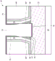
Fig. 10A and 10B illustrate a main etch of the gate stack 60. The corresponding step is shown as step 218 in the process flow 200 shown in fig. 15. Fig. 10A and 10B show sectional views taken from the same plane containing line a-a and line B-B in fig. 8D, respectively. The main etch removes a portion of the gate electrode in region 69 in fig. 8D and serves to cut replacement gate stack 60 in fig. 8D into two portions, each serving as a replacement gate electrode for one of finfets 66A and 66B, as shown in fig. 8D and 10B. Accordingly, the corresponding step is referred to as a cut metal (or cut metal gate) process. The etching produces openings 72 as shown in fig. 10A and 10B. According to some embodiments, the opening 72 extends into the STI region 22, and may extend slightly into the STI region 22.
According to some embodiments of the invention, the main etch comprises a plurality of etch deposition cycles, each cycle comprising an etch step and a polymer deposition step. According to some embodiments of the invention, a compound selected from, but not limited to, Cl is used2、BCl3、Ar、CH4、CF4And combinations thereof. The etching may be performed at a pressure in a range between about 3mTorr and about 10 mTorr. The RF power is applied in the main etch and may range between about 500 watts and about 900 watts. A bias of less than about 150 watts may also be applied.
A polymer layer 70 is deposited, the polymer layer 70 including portions on the sidewalls of the openings 72 to protect the sidewalls so that when the openings 72 extend downward, the upper portions of the openings 72 do not expand laterally. According to some embodiments of the invention, the use comprises SiCl4、O2Ar, etc. to effect deposition of the polymer layer 70. The deposition may be performed at a pressure in a range between about 2mTorr and about 15mTorr, an RF power in a range between about 400 watts and about 900 watts, and a bias voltage of less than about 150 watts. The resulting polymer layer 70 contains elements of silicon (Si), oxygen (O) and carbon (C). In addition, the polymer layer 70 includes SiO in which other elements are mixed2
Each of the etch deposition cycles causes the opening 72 to extend further down until the STI region 22 is exposed. The gate spacers 38 are exposed by etching in each cycle and are then covered by a subsequently deposited polymer layer 70. The etch is anisotropic and thus the sidewalls of the opening 72 are substantially vertical. The polymer layer 70 includes a top horizontal portion on top of the gate spacers 38, ILD48 and CESL 46 and a bottom horizontal portion at the bottom of the opening 72. There may be three or four (or fewer or more) etch deposition cycles. After each cycle or after the final cycle is carried out, it is possible, for example, to use gas O2、N2And H2The post-etch curing is performed. The pressure of the curing gas may be in a range between about 3mTorr and about 10 mTorr. RF power may be applied during curing and may range between about 500 watts and about 900 watts. Curing removes chlorine-containing polymers formed during the cycle.
Since the etching is anisotropic, the footing portions 60 'are not etched due to the shielding of the gate spacers 38 that overlap the footing portions 60'. The footing portion 60' includes portions of the high-k dielectric layer 52 and some remaining portions of the metal gate electrode 56. The remaining portion of the metal gate electrode 56 may comprise TSN, TaN and/or TiN or more, depending on the width of the footer portion 60'.
The polymer layer 70 formed in the previous process has an upper portion 70A located in the opening 72 and a lower portion 70B located below the upper portion 70A. The thickness T2 of lower portion 70B is less than the thickness T1 of portion 70A. For example, the thickness T2 may be less than about 50% of the thickness T1, and may be less than about 30% of the thickness T1. Moreover, the upper portion 70A may have a substantially uniform thickness, while the lower portion 70B may have a lesser and lesser thickness as the depth into the opening 72 increases.
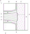
Next, an isotropic wet etch process is performed to thin at least a lower portion 70B (relatively thin) of the polymer layer 70 such that the footing portion 60' is exposed. The resulting structure is shown in fig. 11. The corresponding step is shown as step 220 in the process flow 200 shown in fig. 15. The thicker portions of the polymer layer 70 (including the horizontal portion and the upper portion 70A) are thinned and may not be completely removed. According to some embodiments of the invention, the wet etch is performed using a chemical solution that may be dilute HF. The etching may be performed at a temperature in a range between about 20 ℃ and about 30 ℃, and the etching time may be in a range between about 30 seconds and about 60 seconds.
During the wet etch, the etchant is selected such that the polymer layer 70 is partially etched, while the material in the footing portion 60' is not substantially etched. This can be achieved, for example, by adjusting the concentration of the etching solution (such as HF) to be sufficiently low. According to alternative embodiments, the weight ratio of water to HF in the diluted HF is greater than about 1500:1 and may range between about 1500:1 and about 2500:1 in the etching solution. It should be appreciated that the effect of the etch is related to the concentration of the dilute HF, and that high concentrations, e.g., about 500:1 or higher, may result in the removal of all of the polymer layer 70 and the footing portion 60' and damage to the spacer 38. Therefore, the concentration of diluted HF is chosen to be sufficiently low.
Next, an additional etch is performed to remove portions of the gate electrode 56 in the footer gate stack portion 60'. The corresponding step is shown as step 222 in the process flow 200 shown in fig. 15. The etching is represented by arrows 74 in fig. 12A. The high-k dielectric layer 52 is not etched and remains in the final structure. As can be appreciated from fig. 12A and 8D, high-k dielectric layer 52 of the gate stack of transistor 66A and high-k dielectric layer 52 of the gate stack of transistor 66B are physically connected by the remaining high-k dielectric layer 52 in region 69 (fig. 8D). Since high-k dielectric layer 52 is non-conductive, although the remaining portion of high-k dielectric layer 52 physically connects the gate stack of transistor 66A (fig. 10B and 8D) to the gate stack of transistor 66B, there is no electrical connection.
Referring back to FIG. 12A, etch process 74 may be a dry etch process using NF3As an etching gas. NF3May be in a range between about 1000 and about 2000 mTorr. The temperature of the corresponding wafer is in a range between about 50 ℃ and about 75 ℃Inside the enclosure. The etch time may be in a range between about 60 seconds and about 180 seconds. By etching the metal layer and leaving the high-k dielectric layer 52, the high-k dielectric layer 52 may serve as a protective layer for reducing lateral etching, particularly in the footing region. Also, to leave the high-k dielectric layer 52 unetched, the etching may be gentle and damage to the hard mask (62 in fig. 10B) is reduced due to the gentle etching.
The etching of TiN, TaN, and TSN in the portion of the gate electrode 56 located in the pedestal portion 60' may be represented using the following equations:
TiN+NF+F->TiF (gas) + N2
TaN+NF+F->TaF (gas) + N2
TiSiN+NF+F->TiF (gas) + SiF (gas) + N2
The products of the etching are gaseous and can therefore be removed.
The use of oxygen (O) may also be practiced2) As a curing step for the process gas. The curing may last for a period of time between about 10 seconds and about 40 seconds. Curing may also be skipped. Next, the use of NF may be performed after the oxygen cure3Another etching of (2). Using NF3The etch of (a) may be used with a previous etch (which also uses NF)3Implemented) similar process conditions. And use of NF3The etch in combination with the oxygen cure can effectively etch TiN, TaN and TSN, particularly TaN, which are generally difficult to etch.
According to an alternative embodiment of the present invention, instead of performing the steps shown in fig. 11 and 12A, a wet etch is performed for thinning the polymer layer 70 (fig. 10A), and the etching solution is adjusted such that the etching solution simultaneously attacks the exposed footing portions 60' (including the gate electrode 56 and the high-k dielectric layer 52). In the resulting structure, the footing portion 60' is removed, and the resulting structure is shown in FIG. 12B. According to some embodiments of the invention, the use comprises ammonia fluoride (NH)4F) The wet etching is performed with the chemical solution of (1). NH (NH)4The concentration of F is adjusted to be high enough so that it can etch the polymer layer 70 and the footer gate stack portion 60'. For example, NH4The concentration of F may be greater than about18%, and may range between about 18% and about 25%. It should be understood that NH4The concentration of F affects the results, and low concentrations may not be able to etch some metal layers such as TaN. When the metal layer is not etched, the high-k dielectric layer 52 will also be protected by the metal layer. Thus, to effectively remove the footer gate stack portion 60', NH is selected based on the material and composition of the footer portion 604F concentration to ensure efficient etching. The etching may be performed at a temperature in a range between about 20 ℃ and about 30 ℃, and the etching time may be in a range between about 10 seconds and about 30 seconds.
According to some embodiments of the present invention, after forming the structure as shown in fig. 12A or 12B, the remaining polymer layer 70 is removed, for example, using ultra-dilute HF as an etch chemistry. The resulting structures are shown in fig. 13A and 13B, respectively. The corresponding step is shown as step 224 in the process flow 200 shown in fig. 15. According to an alternative embodiment of the invention, the etching of the polymer layer 70 is skipped and the polymer layer 70 will remain in the final structure. Thus, step 224 in FIG. 15 is shown in a dashed box to indicate that it may or may not be implemented.
Fig. 14A, 14B, 14C and 14D illustrate the formation of dielectric (isolation) regions 76. The corresponding step is shown as step 226 in the process flow 200 shown in fig. 15. Fig. 14D shows a top view of the resulting structure showing isolation regions 76 separating the gate stacks of finfets 66A and 66B. Fig. 14A and 14B are taken from a plane containing line a-a in fig. 14D. FIG. 14C is taken from a plane containing line B-B in FIG. 14D.
The formation of the dielectric (isolation) regions 76 may include depositing a dielectric material into the openings 72 (fig. 13A and 13B) and performing a planarization, such as a CMP or mechanical polish, to remove excess portions of the dielectric material. The filling method may include low pressure chemical vapor deposition, spin coating, Plasma Enhanced Chemical Vapor Deposition (PECVD), etc. The fill material may include silicon nitride, silicon oxide, silicon carbide, silicon oxynitride, silicon oxycarbide, and the like. Fig. 14A also shows the polymer layers 70 using dashed lines to indicate that they may be removed or may remain in the final structure. In fig. 14A, the high-k dielectric layer 52 remains and overlaps the overhang portion of the gate spacer 38.
Fig. 14B illustrates the structure after filling a dielectric material into the opening 72 in fig. 13B, in accordance with some embodiments. The polymer layers 70 are also shown with dashed lines to indicate that they may be removed or may remain in the final structure. In fig. 14B, no high-k dielectric layer remains, and dielectric region 76 extends into the foot region.
Fig. 14C shows a cross-sectional view taken from a plane containing line B-B in fig. 14D. Throughout the description, the combination of the dielectric region 76 and the polymer layer 70 (if remaining) is referred to as an isolation region 78 (fig. 14D), the isolation region 78 separating the gate stacks of the finfets 66A and 66B from each other as replacement gate stacks 60A and 60B. In subsequent steps, more upper ILD (not shown) is formed, and gate contact plugs (not shown) contacting the gate stacks 60A and 60B are formed over the gate stacks 60A and 60B. Silicide regions and source/drain contact plugs (not shown) are also formed over the source/drain regions in contact with the source/drain regions.
Embodiments of the present invention have some advantageous features. By etching the footer portion of the replacement metal gate, footer residue is eliminated and leakage is avoided. Lateral etching is reduced and hard mask loss is also reduced. The process window of the metal cutting process is enlarged.
According to some embodiments of the invention, a method comprises forming a gate stack, the gate stack comprising: a first portion over a portion of the first semiconductor fin; a second portion over a portion of the second semiconductor fin; and a third portion connecting the first portion to the second portion; performing an anisotropic etch on a third portion of the gate stack to form an opening between the first portion and the second portion, wherein a footing portion of the third portion remains after the anisotropic etch; performing an isotropic etch to remove the metal gate portion of the footing portion; and filling the opening with a dielectric material. In an embodiment, the isotropic etching includes using a material containing NH4Wet etching with chemical solution of F. In the implementation ofIn one example, the isotropic etching includes using a composition comprising NF3Dry etching of the process gas (c). In an embodiment, the method further comprises performing an additional isotropic etch to thin the polymer layer on the sidewalls of the footing portion and expose the footing portion. In an embodiment, an additional isotropic etch is performed using diluted HF, and during the additional isotropic etch, the footing portions are substantially unetched. In an embodiment, the high-k dielectric portion and the metal gate electrode portion in the footer portion of the gate stack are removed in an isotropic etch. In an embodiment, in the isotropic etch, the metal gate electrode portion in the footer portion of the gate stack is removed and the high-k dielectric portion in the footer portion of the gate stack remains. In an embodiment, the dielectric material contacts the high-k dielectric portion.
According to some embodiments of the invention, the method comprises forming a gate stack between the first gate spacer and the second gate spacer, the gate stack comprising: a gate dielectric; and a metal electrode over the gate dielectric; etching a first portion of the gate stack to expose sidewalls of the first gate spacer and the second gate spacer; depositing a polymer layer on sidewalls of the first gate spacer and the second gate spacer; thinning the polymer layer to expose a footer portion of the gate stack, wherein the footer portion overlaps a portion of the first gate spacer; and etching the remaining portion of the metal electrode in the footing portion. In an embodiment, a portion of the gate dielectric in the footer portion remains after etching the remaining portion of the metal electrode. In an embodiment, thinning the polymer layer is performed using a diluted HF solution as an etchant. In an embodiment, in thinning the polymer layer, the footing portions are substantially unetched. In an embodiment, etching the remaining portion of the metal electrode comprises using NF3As a first etching step of an etching gas. In an embodiment, the method further comprises: after the first etching step: performing a curing step using oxygen as a process gas, wherein a remaining portion of the gate stack is exposed to oxygen; and use of NF3The second etching step is performed as an etching gas. In an embodiment, the method further comprises coupling the mediaThe electrical material fills into the opening left by the etched first portion of the gate stack. In an embodiment, the gate stack further includes a second portion and a third portion connected by the first portion, and each of the second portion and the third portion is a gate electrode of a transistor.
According to some embodiments of the invention, a method includes forming a gate stack including a gate dielectric and a gate electrode over the gate dielectric, wherein each of the gate dielectric and the gate electrode includes: a first portion over a portion of the first semiconductor fin; a second portion over a portion of the second semiconductor fin; and a third portion connecting the first portion to the second portion; etching a third portion of the gate electrode to electrically disconnect the first portion of the gate electrode from the second portion of the gate electrode, wherein the third portion of the gate dielectric comprises a remaining portion after the etching, and wherein the first portion of the gate dielectric is physically connected to the second portion of the gate dielectric; and filling the opening left by the third portion of the gate electrode with a dielectric material. In an embodiment, the method further comprises forming a gate spacer on a sidewall of the gate stack, wherein a remaining portion of the third portion of the gate dielectric overlaps the gate spacer. In an embodiment, etching the third portion of the gate electrode comprises: anisotropically etching to form an opening, wherein the anisotropically etching is performed until reaching a top surface of the shallow trench isolation region under the gate electrode; and isotropic etching to remove the remaining portion of the gate electrode. In the examples, NF was used3Isotropic etching is performed as an etching gas.
The foregoing has outlined features of several embodiments so that those skilled in the art may better understand the aspects of the present invention. Those skilled in the art should appreciate that they may readily use the present disclosure as a basis for designing or modifying other processes and structures for carrying out the same purposes and/or achieving the same advantages of the embodiments introduced by oneself. Those skilled in the art should also realize that such equivalent constructions do not depart from the spirit and scope of the present disclosure, and that they may make various changes, substitutions, and alterations herein without departing from the spirit and scope of the present disclosure.

Claims (20)

1. A method of forming a transistor, comprising:
forming a gate stack, the gate stack comprising:
a first portion over a portion of the first semiconductor fin;
a second portion over a portion of the second semiconductor fin; and
a third portion connecting the first portion to the second portion;
forming gate spacers on sidewalls of the gate stack;
performing an anisotropic etch on a third portion of the gate stack to form an opening between the first portion and the second portion, wherein, after the anisotropic etch, a footer portion of the third portion remains and is covered by a polymer layer, and the footer portion of the third portion overlaps with a portion of the gate spacer;
performing an isotropic etch to remove a metal gate portion of the footing portion; and
the opening is filled with a dielectric material.
2. The method of claim 1, wherein the isotropic etching comprises using a material comprising ammonium fluoride (NH)4F) Wet etching of the chemical solution of (4).
3. The method of claim 1, wherein the isotropic etching comprises using a mask comprising NF3Dry etching of the process gas (c).
4. The method of claim 3, further comprising performing an additional isotropic etch to thin the polymer layer on the sidewalls of the footing portion and expose the footing portion.
5. The method of claim 4, wherein the additional isotropic etching is performed using diluted HF and the footing portions are not etched during the additional isotropic etching.
6. The method of claim 1, wherein in the isotropic etch, a high-k dielectric portion and a metal gate electrode portion in the footer portion of the gate stack are removed.
7. The method of claim 1, wherein in the isotropic etch, a metal gate electrode portion in the footer portion of the gate stack is removed and a high-k dielectric portion in the footer portion of the gate stack remains.
8. The method of claim 7, wherein the dielectric material contacts the high-k dielectric portion.
9. A method of forming a transistor, comprising:
forming a gate stack between the first gate spacer and the second gate spacer, the gate stack comprising:
a gate dielectric; and
a metal electrode over the gate dielectric;
etching a first portion of the gate stack to expose sidewalls of the first and second gate spacers;
depositing a polymer layer on sidewalls of the first and second gate spacers; thinning the polymer layer to expose a footing portion of the gate stack, wherein the footing portion overlaps a portion of the first gate spacer; and
etching a remaining portion of the metal electrode in the footing portion.
10. The method of claim 9, wherein a portion of the gate dielectric in the footer portion remains after etching the remaining portion of the metal electrode.
11. The method according to claim 9, wherein thinning the polymer layer is performed using a diluted HF solution as an etchant.
12. The method of claim 9, wherein the footing portions are not etched in the thinning of the polymer layer.
13. The method of claim 9, wherein etching the remaining portion of the metal electrode comprises using NF3As a first etching step of an etching gas.
14. The method of claim 13, further comprising:
after the first etching step:
performing a curing step using oxygen as a process gas, wherein a remaining portion of the gate stack is exposed to oxygen; and
using NF3The second etching step is performed as an etching gas.
15. The method of claim 9, further comprising filling a dielectric material into an opening left by the etched first portion of the gate stack.
16. The method of claim 9, wherein the gate stack further comprises a second portion and a third portion connected by the first portion, and each of the second portion and the third portion is a gate electrode of a transistor.
17. A method of forming a transistor, comprising:
forming a gate stack over a semiconductor substrate, the gate stack comprising a gate dielectric and a gate electrode over the gate dielectric, wherein each of the gate dielectric and the gate electrode comprises:
a first portion over a portion of the first semiconductor fin;
a second portion over a portion of the second semiconductor fin; and
a third portion connecting the first portion to the second portion;
etching a third portion of the gate electrode to electrically disconnect the first portion of the gate electrode from the second portion of the gate electrode, wherein the third portion of the gate dielectric comprises the remaining portion after the etching in a vertical plane between and parallel to a lengthwise direction of the first and second semiconductor fins, and wherein the first portion of the gate dielectric is physically connected to the second portion of the gate dielectric by the remaining portion, and wherein the vertical plane is perpendicular to a major bottom surface of the semiconductor substrate; and
filling the opening left by the third portion of the gate electrode with a dielectric material.
18. The method of claim 17, further comprising forming gate spacers on sidewalls of the gate stack, wherein remaining portions of the third portion of the gate dielectric overlap the gate spacers.
19. The method of claim 17, wherein etching the third portion of the gate electrode comprises:
anisotropically etching to form an opening, wherein the anisotropically etching is performed until reaching a top surface of a shallow trench isolation region under the gate electrode; and
an isotropic etch to remove remaining portions of the gate electrode.
20. The method of claim 19, wherein NF is used3The isotropic etching is performed as an etching gas.
CN201810875547.4A 2017-09-29 2018-08-03 Footing removal in metal cutting processes Active CN109585293B (en)

Applications Claiming Priority (4)

Application Number Priority Date Filing Date Title
US201762565532P 2017-09-29 2017-09-29
US62/565,532 2017-09-29
US15/966,437 2018-04-30
US15/966,437 US10811320B2 (en) 2017-09-29 2018-04-30 Footing removal in cut-metal process

Publications (2)

Publication Number Publication Date
CN109585293A CN109585293A (en) 2019-04-05
CN109585293B true CN109585293B (en) 2021-12-24

Family

ID=65728149

Family Applications (1)

Application Number Title Priority Date Filing Date
CN201810875547.4A Active CN109585293B (en) 2017-09-29 2018-08-03 Footing removal in metal cutting processes

Country Status (3)

Country Link
US (1) US20240096707A1 (en)
CN (1) CN109585293B (en)
DE (1) DE102018122665B4 (en)

Families Citing this family (4)

* Cited by examiner, † Cited by third party
Publication number Priority date Publication date Assignee Title
US10236213B1 (en) 2018-03-12 2019-03-19 Globalfoundries Inc. Gate cut structure with liner spacer and related method
DE102019101555B4 (en) * 2018-09-28 2023-01-12 Taiwan Semiconductor Manufacturing Company, Ltd. METAL GATE CUTTING SHAPE
DE102020125324A1 (en) * 2020-02-26 2021-08-26 Taiwan Semiconductor Manufacturing Co., Ltd. Partly directional etching process and the resulting structures
CN113764272B (en) * 2020-06-01 2024-04-26 中芯国际集成电路制造(上海)有限公司 Semiconductor structure and method of forming the same

Citations (4)

* Cited by examiner, † Cited by third party
Publication number Priority date Publication date Assignee Title
CN104051266A (en) * 2013-03-11 2014-09-17 台湾积体电路制造股份有限公司 Fin shape for fin field-effect transistors and method of forming
US9553090B2 (en) * 2015-05-29 2017-01-24 Taiwan Semiconductor Manufacturing Company, Ltd. Structure and formation method of semiconductor device structure
CN106898610A (en) * 2015-12-17 2017-06-27 台湾积体电路制造股份有限公司 Semiconductor devices and its manufacture method
CN109326562A (en) * 2017-07-31 2019-02-12 台湾积体电路制造股份有限公司 Metal gate structure, semiconductor device and method of making the same

Family Cites Families (133)

* Cited by examiner, † Cited by third party
Publication number Priority date Publication date Assignee Title
US4528066A (en) * 1984-07-06 1985-07-09 Ibm Corporation Selective anisotropic reactive ion etching process for polysilicide composite structures
US5498566A (en) * 1993-11-15 1996-03-12 Lg Semicon Co., Ltd. Isolation region structure of semiconductor device and method for fabricating the same
US5811347A (en) * 1996-04-29 1998-09-22 Advanced Micro Devices, Inc. Nitrogenated trench liner for improved shallow trench isolation
US5963789A (en) * 1996-07-08 1999-10-05 Kabushiki Kaisha Toshiba Method for silicon island formation
US6060375A (en) * 1996-07-31 2000-05-09 Lsi Logic Corporation Process for forming re-entrant geometry for gate electrode of integrated circuit structure
US6097076A (en) * 1997-03-25 2000-08-01 Micron Technology, Inc. Self-aligned isolation trench
US7157385B2 (en) * 2003-09-05 2007-01-02 Micron Technology, Inc. Method of depositing a silicon dioxide-comprising layer in the fabrication of integrated circuitry
TWI246633B (en) * 1997-12-12 2006-01-01 Applied Materials Inc Method of pattern etching a low k dielectric layen
US5943585A (en) * 1997-12-19 1999-08-24 Advanced Micro Devices, Inc. Trench isolation structure having low K dielectric spacers arranged upon an oxide liner incorporated with nitrogen
TW362289B (en) * 1997-12-22 1999-06-21 United Microelectronics Corp Manufacturing method of metal oxide semiconductor field effect transistor
US6093655A (en) * 1998-02-12 2000-07-25 Micron Technology, Inc. Plasma etching methods
US6268637B1 (en) * 1998-10-22 2001-07-31 Advanced Micro Devices, Inc. Method of making air gap isolation by making a lateral EPI bridge for low K isolation advanced CMOS fabrication
JP4221859B2 (en) * 1999-02-12 2009-02-12 株式会社デンソー Manufacturing method of semiconductor device
US6300219B1 (en) * 1999-08-30 2001-10-09 Micron Technology, Inc. Method of forming trench isolation regions
US6251750B1 (en) * 1999-09-15 2001-06-26 United Microelectronics Corp. Method for manufacturing shallow trench isolation
US6433371B1 (en) * 2000-01-29 2002-08-13 Advanced Micro Devices, Inc. Controlled gate length and gate profile semiconductor device
US6830977B1 (en) * 2000-08-31 2004-12-14 Micron Technology, Inc. Methods of forming an isolation trench in a semiconductor, methods of forming an isolation trench in a surface of a silicon wafer, methods of forming an isolation trench-isolated transistor, trench-isolated transistor, trench isolation structures formed in a semiconductor, memory cells and drams
US6433871B1 (en) * 2001-05-25 2002-08-13 Advanced Micron Devices, Inc. Method of using scatterometry measurements to determine and control gate electrode profiles
DE10162065A1 (en) * 2001-12-17 2003-06-26 Infineon Technologies Ag Process for anisotropic deep trench etching in a silicon substrate comprises deep trench etching in the silicon substrate up to a prescribed etching depth so that the re-deposit is replaced by a protective layer for side wall passivation
US6660598B2 (en) * 2002-02-26 2003-12-09 International Business Machines Corporation Method of forming a fully-depleted SOI ( silicon-on-insulator) MOSFET having a thinned channel region
US6979652B2 (en) * 2002-04-08 2005-12-27 Applied Materials, Inc. Etching multi-shaped openings in silicon
US20040029389A1 (en) * 2002-08-06 2004-02-12 Winbond Electronics Corporation Method of forming shallow trench isolation structure with self-aligned floating gate
JP2004111429A (en) * 2002-09-13 2004-04-08 Renesas Technology Corp Semiconductor device
US7169695B2 (en) * 2002-10-11 2007-01-30 Lam Research Corporation Method for forming a dual damascene structure
KR100505044B1 (en) * 2002-12-17 2005-07-29 삼성전자주식회사 Cleaning Solution and Method of Cleaning semiconductor device
US7091104B2 (en) * 2003-01-23 2006-08-15 Silterra Malaysia Sdn. Bhd. Shallow trench isolation
KR100503814B1 (en) * 2003-02-04 2005-07-27 동부아남반도체 주식회사 Method for forming gate of semiconductor element
US20040173566A1 (en) * 2003-03-03 2004-09-09 Macronix International Co., Ltd. Method for polymer removal after an etching process
KR100752214B1 (en) * 2003-10-16 2007-08-28 엘지.필립스 엘시디 주식회사 Manufacturing method of transflective liquid crystal display device
US6955964B2 (en) * 2003-11-05 2005-10-18 Promos Technologies, Inc. Formation of a double gate structure
US7247569B2 (en) * 2003-12-02 2007-07-24 International Business Machines Corporation Ultra-thin Si MOSFET device structure and method of manufacture
US6812120B1 (en) * 2004-02-26 2004-11-02 Powerchip Semiconductor Corp. Method of forming floating gate of memory device
US7053010B2 (en) * 2004-03-22 2006-05-30 Micron Technology, Inc. Methods of depositing silicon dioxide comprising layers in the fabrication of integrated circuitry, methods of forming trench isolation, and methods of forming arrays of memory cells
JP4112550B2 (en) * 2004-11-01 2008-07-02 富士通株式会社 Manufacturing method of semiconductor device
US7749911B2 (en) * 2004-11-30 2010-07-06 Taiwan Semiconductor Manufacturing Co., Ltd. Method for forming an improved T-shaped gate structure
US8012847B2 (en) * 2005-04-01 2011-09-06 Micron Technology, Inc. Methods of forming trench isolation in the fabrication of integrated circuitry and methods of fabricating integrated circuitry
KR100655647B1 (en) * 2005-07-04 2006-12-08 삼성전자주식회사 Cleaning liquid composition for semiconductor substrate, manufacturing method thereof, cleaning method of semiconductor substrate using same and manufacturing method of semiconductor device
US7588946B2 (en) * 2005-07-25 2009-09-15 Taiwan Semiconductor Manufacturing Company, Ltd. Controlling system for gate formation of semiconductor devices
US20070059897A1 (en) * 2005-09-09 2007-03-15 Armin Tilke Isolation for semiconductor devices
US7544621B2 (en) * 2005-11-01 2009-06-09 United Microelectronics Corp. Method of removing a metal silicide layer on a gate electrode in a semiconductor manufacturing process and etching method
KR100698078B1 (en) * 2005-11-24 2007-03-23 동부일렉트로닉스 주식회사 Manufacturing Method of Semiconductor Device
KR100758296B1 (en) * 2006-01-31 2007-09-12 삼성전자주식회사 How to form a trench
JP2007221058A (en) * 2006-02-20 2007-08-30 Toshiba Corp Manufacturing method of semiconductor device
US7351664B2 (en) * 2006-05-30 2008-04-01 Lam Research Corporation Methods for minimizing mask undercuts and notches for plasma processing system
KR101033222B1 (en) * 2007-06-29 2011-05-06 주식회사 하이닉스반도체 Method for manufacturing nonvolatile memory device having charge trap layer
JP5130834B2 (en) * 2007-09-05 2013-01-30 ソニー株式会社 Semiconductor device and manufacturing method thereof
US7790559B2 (en) * 2008-02-27 2010-09-07 International Business Machines Corporation Semiconductor transistors having high-K gate dielectric layers and metal gate electrodes
US20090242512A1 (en) * 2008-03-27 2009-10-01 Dalsa Semiconductor Inc. Deep reactive ion etching
US7972968B2 (en) * 2008-08-18 2011-07-05 Applied Materials, Inc. High density plasma gapfill deposition-etch-deposition process etchant
US20100044804A1 (en) * 2008-08-25 2010-02-25 Taiwan Semiconductor Manufacturing Company, Ltd. Novel high-k metal gate structure and method of making
US8319311B2 (en) * 2009-03-16 2012-11-27 Taiwan Semiconductor Manufacturing Company, Ltd. Hybrid STI gap-filling approach
US8258588B2 (en) * 2009-08-07 2012-09-04 Taiwan Semiconductor Manufacturing Company, Ltd. Sealing layer of a field effect transistor
US8076735B2 (en) * 2009-10-02 2011-12-13 United Microelectronics Corp. Semiconductor device with trench of various widths
KR20110042614A (en) * 2009-10-19 2011-04-27 삼성전자주식회사 Semiconductor device and method of forming the same
US9299664B2 (en) * 2010-01-18 2016-03-29 Semiconductor Components Industries, Llc Method of forming an EM protected semiconductor die
US20120077327A1 (en) * 2010-09-29 2012-03-29 International Business Machines Corporation Formation of a Shallow Trench Isolation Structure
US8598675B2 (en) * 2011-02-10 2013-12-03 Taiwan Semiconductor Manufacturing Company, Ltd. Isolation structure profile for gap filling
US8421132B2 (en) * 2011-05-09 2013-04-16 International Business Machines Corporation Post-planarization UV curing of stress inducing layers in replacement gate transistor fabrication
US9184100B2 (en) * 2011-08-10 2015-11-10 United Microelectronics Corp. Semiconductor device having strained fin structure and method of making the same
US8652969B2 (en) * 2011-10-26 2014-02-18 International Business Machines Corporation High aspect ratio and reduced undercut trench etch process for a semiconductor substrate
US20130178055A1 (en) * 2012-01-09 2013-07-11 Globalfoundries Inc. Methods of Forming a Replacement Gate Electrode With a Reentrant Profile
US8741723B2 (en) * 2012-04-25 2014-06-03 Globalfoundries Inc. Methods of forming self-aligned contacts for a semiconductor device
US8803249B2 (en) * 2012-08-09 2014-08-12 Taiwan Semiconductor Manufacturing Co., Ltd. Profile pre-shaping for replacement poly gate interlayer dielectric
US9219153B2 (en) * 2013-08-21 2015-12-22 Globalfoundries Inc. Methods of forming gate structures for FinFET devices and the resulting semiconductor products
US9991285B2 (en) * 2013-10-30 2018-06-05 Taiwan Semiconductor Manufacturing Company, Ltd. Mechanisms for forming FinFET device
US10825738B2 (en) * 2013-11-28 2020-11-03 Institute of Microelectronics, Chinese Academy of Sciences Semiconductor arrangements and methods of manufacturing the same
US9553171B2 (en) * 2014-02-14 2017-01-24 Taiwan Semiconductor Manufacturing Co., Ltd. Fin field effect transistor (FinFET) device and method for forming the same
US9620621B2 (en) * 2014-02-14 2017-04-11 Taiwan Semiconductor Manufacturing Company Ltd. Gate structure of field effect transistor with footing
US9324710B2 (en) * 2014-02-24 2016-04-26 International Business Machines Corporation Very planar gate cut post replacement gate process
US10084060B2 (en) * 2014-08-15 2018-09-25 Taiwan Semiconductor Manufacturing Company Ltd. Semiconductor structure and manufacturing method of the same
US9373641B2 (en) * 2014-08-19 2016-06-21 International Business Machines Corporation Methods of forming field effect transistors using a gate cut process following final gate formation
US9935126B2 (en) * 2014-09-08 2018-04-03 Infineon Technologies Ag Method of forming a semiconductor substrate with buried cavities and dielectric support structures
KR102222818B1 (en) * 2014-10-06 2021-03-04 삼성전자주식회사 Methods of manufacturing a semiconductor device
US10164049B2 (en) * 2014-10-06 2018-12-25 Taiwan Semiconductor Manufacturing Company, Ltd. Structure and formation method of semiconductor device with gate stack
US9496402B2 (en) * 2014-10-17 2016-11-15 Taiwan Semiconductor Manufacturing Company, Ltd. Metal gate with silicon sidewall spacers
US9214358B1 (en) * 2014-10-30 2015-12-15 Taiwan Semiconductor Manufacturing Company, Ltd. Equal gate height control method for semiconductor device with different pattern densites
KR102217246B1 (en) * 2014-11-12 2021-02-18 삼성전자주식회사 Integrated circuit device and method of manufacturing the same
KR102290793B1 (en) * 2014-12-18 2021-08-19 삼성전자주식회사 Semiconductor device, methods of forming patterns for semiconductor device, and methods of manufacturing semiconductor devices
US9929242B2 (en) * 2015-01-12 2018-03-27 Taiwan Semiconductor Manufacturing Co., Ltd. Semiconductor device and manufacturing method thereof
US9331074B1 (en) * 2015-01-30 2016-05-03 Taiwan Semiconductor Manufacturing Co., Ltd. Semiconductor device and manufacturing method thereof
KR102312346B1 (en) * 2015-02-23 2021-10-14 삼성전자주식회사 Methods of Fabricating Semiconductor Devices
US9577101B2 (en) * 2015-03-13 2017-02-21 Taiwan Semiconductor Manufacturing Company, Ltd. Source/drain regions for fin field effect transistors and methods of forming same
US9748394B2 (en) * 2015-05-20 2017-08-29 Taiwan Semiconductor Manufacturing Co., Ltd. FinFET having a multi-portioned gate stack
KR102258109B1 (en) * 2015-06-08 2021-05-28 삼성전자주식회사 Semiconductor device blocking a leakage current and method for fabricating the same
KR102505242B1 (en) * 2015-07-21 2023-03-06 삼성전자주식회사 Semiconductor device and method for fabricating the same
KR102292812B1 (en) * 2015-08-18 2021-08-23 삼성전자주식회사 Semiconductor device
KR102292813B1 (en) * 2015-10-14 2021-08-23 삼성전자주식회사 Semiconductor device and method for fabricating the same
US10096712B2 (en) * 2015-10-20 2018-10-09 Taiwan Semiconductor Manufacturing Company, Ltd. FinFET device and method of forming and monitoring quality of the same
KR20170047953A (en) * 2015-10-26 2017-05-08 삼성전자주식회사 Semiconductor device and method of fabricating the same
US9659930B1 (en) * 2015-11-04 2017-05-23 Taiwan Semiconductor Manufacturing Co., Ltd. Semiconductor device and manufacturing method thereof
US20170148682A1 (en) * 2015-11-19 2017-05-25 International Business Machines Corporation Finfet with post-rmg gate cut
US9431399B1 (en) * 2015-12-15 2016-08-30 International Business Machines Corporation Method for forming merged contact for semiconductor device
US9985031B2 (en) * 2016-01-21 2018-05-29 Taiwan Semiconductor Manufacturing Co., Ltd. Integrated circuit and manufacturing method thereof
US9773912B2 (en) * 2016-01-28 2017-09-26 Taiwan Semiconductor Manufacturing Company Limited Semiconductor device and manufacturing method thereof
US9768170B2 (en) * 2016-02-05 2017-09-19 Taiwan Semiconductor Manufacturing Co., Ltd. Fin field effect transistor and method for fabricating the same
US9847330B2 (en) * 2016-02-05 2017-12-19 Taiwan Semiconductor Manufacturing Co., Ltd. Fin field effect transistor and method for fabricating the same
US10269793B2 (en) * 2016-04-28 2019-04-23 Taiwan Semiconductor Manufacturing Company, Ltd. Source/drain regions in fin field effect transistors (FinFETs) and methods of forming same
US9899266B2 (en) * 2016-05-02 2018-02-20 Taiwan Semiconductor Manufacturing Company, Ltd. FinFET structures and methods of forming the same
US9917085B2 (en) * 2016-05-31 2018-03-13 Taiwan Semiconductor Manufacturing Company, Ltd. Metal gate isolation structure and method forming same
US10103246B2 (en) * 2016-06-09 2018-10-16 International Business Machines Corporation Fabrication of a vertical fin field effect transistor (vertical finFET) with a self-aligned gate and fin edges
US9960074B2 (en) * 2016-06-30 2018-05-01 Taiwan Semiconductor Manufacturing Company, Ltd. Integrated bi-layer STI deposition
TWI707473B (en) * 2016-11-23 2020-10-11 聯華電子股份有限公司 Semiconductor device and manufacturing method thereof
US10079289B2 (en) * 2016-12-22 2018-09-18 Taiwan Semiconductor Manufacturing Co., Ltd. Metal gate structure and methods thereof
US10263090B2 (en) * 2017-04-24 2019-04-16 Taiwan Semiconductor Manufacturing Co., Ltd. Semiconductor device and manufacturing method thereof
US10354997B2 (en) * 2017-04-28 2019-07-16 Taiwan Semiconductor Manufacturing Company, Ltd. Method for manufacturing semiconductor device with replacement gates
US10115724B1 (en) * 2017-06-27 2018-10-30 International Business Machines Corporation Double diffusion break gate structure without vestigial antenna capacitance
DE102017126027B4 (en) * 2017-07-31 2022-02-24 Taiwan Semiconductor Manufacturing Co., Ltd. Metal gate structure and method
US10535654B2 (en) * 2017-08-30 2020-01-14 Taiwan Semiconductor Manufacturing Co., Ltd. Cut metal gate with slanted sidewalls
US20190096751A1 (en) * 2017-09-26 2019-03-28 Microchip Technology Incorporated Dual Damascene Process for Forming Vias and Interconnects in an Integrated Circuit Structure
US10811320B2 (en) * 2017-09-29 2020-10-20 Taiwan Semiconductor Manufacturing Company, Ltd. Footing removal in cut-metal process
US10325912B2 (en) * 2017-10-30 2019-06-18 Taiwan Semiconductor Manufacturing Co., Ltd. Semiconductor structure cutting process and structures formed thereby
US10483369B2 (en) * 2017-10-30 2019-11-19 Globalfoundries Inc. Methods of forming replacement gate structures on transistor devices
US10453936B2 (en) * 2017-10-30 2019-10-22 Globalfoundries Inc. Methods of forming replacement gate structures on transistor devices
US10163640B1 (en) * 2017-10-31 2018-12-25 Taiwan Semiconductor Manufacturing Company, Ltd. Gate isolation plugs structure and method
US10388652B2 (en) * 2017-11-14 2019-08-20 Globalfoundries Inc. Intergrated circuit structure including single diffusion break abutting end isolation region, and methods of forming same
US10468527B2 (en) * 2017-11-15 2019-11-05 Taiwan Semiconductor Manufacturing Co., Ltd. Metal gate structure and methods of fabricating thereof
US10978351B2 (en) * 2017-11-17 2021-04-13 Taiwan Semiconductor Manufacturing Co., Ltd. Etch stop layer between substrate and isolation structure
US10319581B1 (en) * 2017-11-30 2019-06-11 Taiwan Semiconductor Manufacturing Co., Ltd. Cut metal gate process for reducing transistor spacing
KR20190081071A (en) * 2017-12-29 2019-07-09 삼성전자주식회사 Semiconductor device
US10236213B1 (en) * 2018-03-12 2019-03-19 Globalfoundries Inc. Gate cut structure with liner spacer and related method
KR20190130348A (en) * 2018-05-14 2019-11-22 삼성전자주식회사 Semiconductor devices
US10418285B1 (en) * 2018-05-30 2019-09-17 Globalfoundries Inc. Fin field-effect transistor (FinFET) and method of production thereof
KR102636464B1 (en) * 2018-06-12 2024-02-14 삼성전자주식회사 Semiconductor device having gate isolation layer and method of manufacturing the same
US10658491B2 (en) * 2018-06-15 2020-05-19 Taiwan Semiconductor Manufacturing Company, Ltd. Controlling profiles of replacement gates
US10854603B2 (en) * 2018-06-29 2020-12-01 Taiwan Semiconductor Manufacturing Company, Ltd. Semiconductor device and method
US10714347B2 (en) * 2018-10-26 2020-07-14 Taiwan Semiconductor Manufacturing Company, Ltd. Cut metal gate processes
US11217486B2 (en) * 2018-10-31 2022-01-04 Taiwan Semiconductor Manufacturing Company, Ltd. Semiconductor device and method
TWI804632B (en) * 2019-06-05 2023-06-11 聯華電子股份有限公司 Semiconductor device and method for fabricating the same
US11374110B2 (en) * 2020-02-26 2022-06-28 Taiwan Semiconductor Manufacturing Co., Ltd. Partial directional etch method and resulting structures
DE102020125324A1 (en) * 2020-02-26 2021-08-26 Taiwan Semiconductor Manufacturing Co., Ltd. Partly directional etching process and the resulting structures
CN113990799B (en) * 2020-07-27 2022-12-16 长鑫存储技术有限公司 Preparation method of semiconductor device and semiconductor device
US12364002B2 (en) * 2021-06-25 2025-07-15 Intel Corporation Integrated circuit structures having metal gates with tapered plugs
US20240105504A1 (en) * 2022-09-23 2024-03-28 Vanguard International Semiconductor Corporation Semiconductor device and method of manufacturing the same

Patent Citations (4)

* Cited by examiner, † Cited by third party
Publication number Priority date Publication date Assignee Title
CN104051266A (en) * 2013-03-11 2014-09-17 台湾积体电路制造股份有限公司 Fin shape for fin field-effect transistors and method of forming
US9553090B2 (en) * 2015-05-29 2017-01-24 Taiwan Semiconductor Manufacturing Company, Ltd. Structure and formation method of semiconductor device structure
CN106898610A (en) * 2015-12-17 2017-06-27 台湾积体电路制造股份有限公司 Semiconductor devices and its manufacture method
CN109326562A (en) * 2017-07-31 2019-02-12 台湾积体电路制造股份有限公司 Metal gate structure, semiconductor device and method of making the same

Also Published As

Publication number Publication date
DE102018122665A1 (en) 2019-04-04
US20240096707A1 (en) 2024-03-21
CN109585293A (en) 2019-04-05
DE102018122665B4 (en) 2025-07-31

Similar Documents

Publication Publication Date Title
US11854903B2 (en) Footing removal in cut-metal process
US12206011B2 (en) Dummy gate cutting process and resulting gate structures
CN110634799B (en) Method for forming semiconductor device and semiconductor device
US8786019B2 (en) CMOS FinFET device
US11145512B2 (en) Gate isolation plugs structure and method
CN108231588A (en) Transistor and forming method thereof
TW201643966A (en) Fin field effect transistor device and forming method thereof
TW201826336A (en) Semiconductor device and method of manufacturing same
CN110610861A (en) Method for forming semiconductor device
US20240096707A1 (en) Footing Removal in Cut-Metal Process
TW202006830A (en) Semiconductor device and fabrication method thereof
TW201903858A (en) Methods for fabricating semiconductor devices
KR102334898B1 (en) Residue removal in metal gate cutting process
TWI807325B (en) Semiconductor device and method for forming the same
US20250248108A1 (en) Dummy Fin with Reduced Height and Method Forming Same
US12176415B2 (en) Device with a dummy fin contacting a gate isolation region
US12520559B2 (en) Semiconductor device

Legal Events

Date Code Title Description
PB01 Publication
PB01 Publication
SE01 Entry into force of request for substantive examination
GR01 Patent grant
GR01 Patent grant