CN107077262B - Pixelization from capacitive water repellence - Google Patents
Pixelization from capacitive water repellence Download PDFInfo
- Publication number
- CN107077262B CN107077262B CN201580058366.7A CN201580058366A CN107077262B CN 107077262 B CN107077262 B CN 107077262B CN 201580058366 A CN201580058366 A CN 201580058366A CN 107077262 B CN107077262 B CN 107077262B
- Authority
- CN
- China
- Prior art keywords
- touch
- image
- water
- scan
- node electrodes
- Prior art date
- Legal status (The legal status is an assumption and is not a legal conclusion. Google has not performed a legal analysis and makes no representation as to the accuracy of the status listed.)
- Active
Links
Images


Classifications
-
- G—PHYSICS
- G06—COMPUTING OR CALCULATING; COUNTING
- G06F—ELECTRIC DIGITAL DATA PROCESSING
- G06F3/00—Input arrangements for transferring data to be processed into a form capable of being handled by the computer; Output arrangements for transferring data from processing unit to output unit, e.g. interface arrangements
- G06F3/01—Input arrangements or combined input and output arrangements for interaction between user and computer
- G06F3/03—Arrangements for converting the position or the displacement of a member into a coded form
- G06F3/041—Digitisers, e.g. for touch screens or touch pads, characterised by the transducing means
- G06F3/0416—Control or interface arrangements specially adapted for digitisers
- G06F3/0418—Control or interface arrangements specially adapted for digitisers for error correction or compensation, e.g. based on parallax, calibration or alignment
-
- G—PHYSICS
- G06—COMPUTING OR CALCULATING; COUNTING
- G06F—ELECTRIC DIGITAL DATA PROCESSING
- G06F3/00—Input arrangements for transferring data to be processed into a form capable of being handled by the computer; Output arrangements for transferring data from processing unit to output unit, e.g. interface arrangements
- G06F3/01—Input arrangements or combined input and output arrangements for interaction between user and computer
- G06F3/03—Arrangements for converting the position or the displacement of a member into a coded form
- G06F3/033—Pointing devices displaced or positioned by the user, e.g. mice, trackballs, pens or joysticks; Accessories therefor
- G06F3/0354—Pointing devices displaced or positioned by the user, e.g. mice, trackballs, pens or joysticks; Accessories therefor with detection of 2D relative movements between the device, or an operating part thereof, and a plane or surface, e.g. 2D mice, trackballs, pens or pucks
- G06F3/03547—Touch pads, in which fingers can move on a surface
-
- G—PHYSICS
- G06—COMPUTING OR CALCULATING; COUNTING
- G06F—ELECTRIC DIGITAL DATA PROCESSING
- G06F3/00—Input arrangements for transferring data to be processed into a form capable of being handled by the computer; Output arrangements for transferring data from processing unit to output unit, e.g. interface arrangements
- G06F3/01—Input arrangements or combined input and output arrangements for interaction between user and computer
- G06F3/03—Arrangements for converting the position or the displacement of a member into a coded form
- G06F3/041—Digitisers, e.g. for touch screens or touch pads, characterised by the transducing means
- G06F3/0412—Digitisers structurally integrated in a display
-
- G—PHYSICS
- G06—COMPUTING OR CALCULATING; COUNTING
- G06F—ELECTRIC DIGITAL DATA PROCESSING
- G06F3/00—Input arrangements for transferring data to be processed into a form capable of being handled by the computer; Output arrangements for transferring data from processing unit to output unit, e.g. interface arrangements
- G06F3/01—Input arrangements or combined input and output arrangements for interaction between user and computer
- G06F3/03—Arrangements for converting the position or the displacement of a member into a coded form
- G06F3/041—Digitisers, e.g. for touch screens or touch pads, characterised by the transducing means
- G06F3/0416—Control or interface arrangements specially adapted for digitisers
- G06F3/04166—Details of scanning methods, e.g. sampling time, grouping of sub areas or time sharing with display driving
- G06F3/041662—Details of scanning methods, e.g. sampling time, grouping of sub areas or time sharing with display driving using alternate mutual and self-capacitive scanning
-
- G—PHYSICS
- G06—COMPUTING OR CALCULATING; COUNTING
- G06F—ELECTRIC DIGITAL DATA PROCESSING
- G06F3/00—Input arrangements for transferring data to be processed into a form capable of being handled by the computer; Output arrangements for transferring data from processing unit to output unit, e.g. interface arrangements
- G06F3/01—Input arrangements or combined input and output arrangements for interaction between user and computer
- G06F3/03—Arrangements for converting the position or the displacement of a member into a coded form
- G06F3/041—Digitisers, e.g. for touch screens or touch pads, characterised by the transducing means
- G06F3/044—Digitisers, e.g. for touch screens or touch pads, characterised by the transducing means by capacitive means
- G06F3/0443—Digitisers, e.g. for touch screens or touch pads, characterised by the transducing means by capacitive means using a single layer of sensing electrodes
Landscapes
- Engineering & Computer Science (AREA)
- General Engineering & Computer Science (AREA)
- Theoretical Computer Science (AREA)
- Human Computer Interaction (AREA)
- Physics & Mathematics (AREA)
- General Physics & Mathematics (AREA)
- Position Input By Displaying (AREA)
Abstract
Description
相关专利申请的交叉引用Cross-references to related patent applications
本专利申请要求于2014年10月27日提交的美国临时专利申请No. 62/069,231的权益,该专利申请的全部公开内容以引用方式并入本文以用于所有目的。This patent application claims the benefit of US Provisional Patent Application No. 62/069,231, filed October 27, 2014, the entire disclosure of which is incorporated herein by reference for all purposes.
技术领域technical field
本发明整体上涉及触摸传感器面板,并且更具体地涉及在像素化自电容触摸传感器面板上排斥水。The present invention relates generally to touch sensor panels, and more particularly to repelling water on pixelated self-capacitance touch sensor panels.
背景技术Background technique
很多类型的输入设备当前可用于在计算系统中执行操作,诸如按钮或按键、鼠标、轨迹球、操纵杆、触摸传感器面板、触摸屏等等。具体地,触摸屏因其在操作方面的简便性和灵活性以及其不断下降的价格而变得日益受欢迎。触摸屏可包括触摸传感器面板和显示设备诸如液晶显示器 (LCD),该触摸传感器面板可以是具有触敏表面的透明面板,该显示设备可部分地或完全被定位在面板的后面,使得触敏表面可覆盖显示设备的可视区域的至少一部分。该触摸屏可允许用户通过使用手指、触笔或其他对象在由显示设备所显示的用户界面(UI)常常指示的位置处触摸该触摸传感器面板来执行各种功能。一般来讲,该触摸屏可识别触摸和触摸在触摸传感器面板上的位置,并且该计算系统然后可根据触摸发生时出现的显示内容来解释该触摸,并且然后可基于触摸来执行一个或多个动作。就一些触摸感测系统而言,检测触摸不需要显示器上的物理触摸。例如,在一些电容式触摸感测系统中,用于检测触摸的边缘电场可能会延伸超过显示器的表面,并且接近表面的对象可能被检测出在表面附近而无需实际接触表面。Many types of input devices are currently available for performing operations in computing systems, such as buttons or keys, mice, trackballs, joysticks, touch sensor panels, touch screens, and the like. In particular, touchscreens are becoming increasingly popular due to their simplicity and flexibility in operation and their falling prices. A touch screen may include a touch sensor panel, which may be a transparent panel with a touch-sensitive surface, and a display device, such as a liquid crystal display (LCD), that may be positioned partially or fully behind the panel so that the touch-sensitive surface may be Covers at least a portion of the viewable area of the display device. The touch screen may allow a user to perform various functions by touching the touch sensor panel with a finger, stylus, or other object at a location often indicated by a user interface (UI) displayed by the display device. In general, the touchscreen can recognize touches and the location of the touches on the touch sensor panel, and the computing system can then interpret the touches from what appears on the display when the touches occur, and can then perform one or more actions based on the touches . With some touch-sensing systems, detecting a touch does not require a physical touch on the display. For example, in some capacitive touch sensing systems, fringing electric fields used to detect touch may extend beyond the surface of the display, and objects approaching the surface may be detected near the surface without actually touching the surface.
该电容触摸传感器面板可由基本上透明或不透明的导电板的矩阵形成,该基本上透明的导电板由材料诸如氧化铟锡(ITO)制成。如上所述,部分由于其基本上透明,因此可将一些电容触摸传感器面板重叠在显示器上,以形成触摸屏。一些触摸屏可通过将触摸感测电路至少部分地集成到显示器像素层叠结构(即,形成显示器像素的堆叠材料层)中来形成。The capacitive touch sensor panel may be formed from a matrix of substantially transparent or opaque conductive plates made of materials such as indium tin oxide (ITO). As mentioned above, some capacitive touch sensor panels can be overlaid on a display to form a touch screen, in part because of their substantial transparency. Some touch screens may be formed by integrating touch-sensing circuitry at least partially into a display pixel stack-up (ie, the stacked layers of material that form the display pixels).
发明内容SUMMARY OF THE INVENTION
一些电容触摸传感器面板可由基本上透明或不透明的导电板的矩阵形成,该基本上透明的导电板由材料诸如氧化铟锡(ITO)制成,而一些触摸屏可通过将触摸感测电路至少部分地集成到显示器像素层叠结构(即,形成显示器像素的堆叠材料层)中来形成。通过检测导电板(触摸节点电极) 的自电容的变化,可在触摸屏上感测触摸事件。在一些示例中,水或水滴可能存在于本公开的触摸屏上。同样有益的是,能够将在触摸屏上可能存在的水(例如,水滴)与手指触摸活动区分开来,前者可被忽略,而后者可被处理为触摸活动。在一些示例中,本公开的触摸屏上的孤立水滴 (即,未接触接地的用户或对象的水滴)可能不会出现在触摸屏的完全自举扫描上,但可能不同程度地出现在触摸屏的部分自举扫描以及互电容扫描上。因此,可使用触摸屏的完全自举扫描和触摸屏的部分自举扫描和/或互电容扫描的比较来识别触摸屏上的水的存在,并将水从可用于分析触摸活动的最终触摸图像忽略或弃去。Some capacitive touch sensor panels may be formed from a matrix of substantially transparent or opaque conductive plates made of materials such as indium tin oxide (ITO), while some touch screens may be formed by incorporating touch sensing circuitry at least partially. It is formed by being integrated into a display pixel stack-up (ie, the stacked layers of material that form the display pixels). Touch events can be sensed on the touch screen by detecting changes in the self-capacitance of the conductive plates (touch node electrodes). In some examples, water or water droplets may be present on the touch screen of the present disclosure. It is also beneficial to be able to distinguish the possible presence of water (eg, water droplets) on the touch screen from finger touch activity, which can be ignored and which can be treated as touch activity. In some examples, isolated water droplets (ie, water droplets that do not contact a grounded user or object) on the touchscreen of the present disclosure may not appear on a full bootstrap scan of the touchscreen, but may appear to varying degrees on a portion of the touchscreen self-guided. Lift scan and mutual capacitance scan. Thus, a comparison of a full bootstrap scan of the touchscreen and a partial bootstrap scan and/or mutual capacitance scan of the touchscreen can be used to identify the presence of water on the touchscreen and ignore or discard water from the final touch image that can be used to analyze touch activity go.
附图说明Description of drawings
图1A-图1C示出了可各自包括根据本公开的示例的示例性触摸屏的示例性移动电话、示例性媒体播放器和示例性便携式计算设备。1A-1C illustrate an example mobile phone, an example media player, and an example portable computing device that may each include an example touchscreen according to examples of the present disclosure.
图2是示出了根据本公开的示例的示例性触摸屏的一个具体实施的示例性计算系统的框图。2 is a block diagram of an exemplary computing system illustrating one implementation of an exemplary touch screen according to an example of the present disclosure.
图3示出了根据本公开的示例的与自电容触摸节点电极和感测电路对应的示例性触摸传感器电路。3 illustrates an example touch sensor circuit corresponding to a self-capacitance touch node electrode and a sense circuit according to an example of the present disclosure.
图4示出了根据本公开的示例的其中公共电极可形成触摸感测系统的触摸感测电路的部分的示例性配置。4 illustrates an example configuration in which a common electrode may form part of a touch-sensing circuit of a touch-sensing system, according to an example of the present disclosure.
图5A示出了根据本公开的示例的其中每个触摸节点电极可被同时驱动和感测的示例性完全自举式触摸屏。5A illustrates an example fully bootstrapped touch screen in which each touch node electrode can be driven and sensed simultaneously, according to examples of the present disclosure.
图5B示出了根据本公开的示例的其中仅一部分触摸节点电极可被同时驱动和感测的示例性部分自举式触摸屏。5B illustrates an example partially bootstrapped touch screen in which only a portion of the touch node electrodes may be driven and sensed simultaneously, according to examples of the present disclosure.
图6A示出了根据本公开的示例的其上可驻留有孤立水滴的示例性完全自举式触摸屏。6A illustrates an exemplary fully bootstrapped touch screen on which isolated water droplets may reside, according to an example of the present disclosure.
图6B示出了根据本公开的示例的其上可驻留有孤立水滴的示例性部分自举式触摸屏。6B illustrates an exemplary partially bootstrapped touch screen on which isolated water droplets may reside, according to an example of the present disclosure.
图6C示出了根据本公开的示例的以互电容配置操作的其上可驻留有孤立水滴的示例性触摸屏。6C illustrates an example touch screen on which isolated water droplets may reside, operating in a mutual capacitance configuration, in accordance with examples of the present disclosure.
图7A示出了根据本公开的示例的具有耦接到适当电路的触摸节点的部分自举式触摸屏的示例性配置。7A illustrates an exemplary configuration of a partially bootstrapped touch screen with touch nodes coupled to appropriate circuitry according to an example of the present disclosure.
图7B示出了根据本公开的示例的可利用开关阵列将适当的电路耦接到触摸节点的部分自举式触摸屏的示例性配置。7B illustrates an exemplary configuration of a partially bootstrapped touch screen that may utilize a switch array to couple appropriate circuitry to touch nodes, according to an example of the present disclosure.
图8A示出了根据本公开的示例的触摸屏上的示例性完全自举扫描。8A illustrates an exemplary full bootstrap scan on a touch screen according to an example of the present disclosure.
图8B示出了根据本公开的示例的触摸屏上的示例性部分自举扫描。8B illustrates an exemplary partial bootstrap scan on a touch screen according to an example of the present disclosure.
图8C示出了根据本公开的示例的触摸屏上的分辨率降低的示例性完全自举扫描。8C illustrates an exemplary full bootstrap scan with reduced resolution on a touch screen according to an example of the present disclosure.
图9A示出了根据本公开的示例的触摸屏上的示例性完全自举扫描。9A illustrates an exemplary full bootstrap scan on a touch screen according to an example of the present disclosure.
图9B示出了根据本公开的示例的触摸屏上的示例性互电容扫描。9B illustrates an example mutual capacitance scan on a touch screen according to an example of the present disclosure.
图9C示出了根据本公开的示例的触摸屏上的分辨率降低的示例性完全自举扫描。9C illustrates an exemplary full bootstrap scan with reduced resolution on a touch screen according to an example of the present disclosure.
图10A示出了根据本公开的示例的示例性基础触摸屏显示帧和触摸帧配置。10A illustrates an example base touch screen display frame and touch frame configuration according to examples of the present disclosure.
图10B示出了根据本公开的示例的图10A中的部分自举扫描步骤的示例性细节。10B shows exemplary details of the partial bootstrap scan step in FIG. 10A according to an example of the present disclosure.
图11A示出了根据本公开的示例的示例性水检测和水排斥显示帧和触摸帧配置。11A illustrates an exemplary water detection and water repelling display frame and touch frame configuration in accordance with an example of the present disclosure.
图11B示出了根据本公开的示例的另一示例性水检测和水排斥显示帧和触摸帧配置。11B illustrates another exemplary water detection and water rejection display frame and touch frame configuration in accordance with examples of the present disclosure.
图11C示出了根据本公开的示例的图11B中的完全自举扫描步骤的示例性细节。FIG. 11C shows exemplary details of the full bootstrap scan step in FIG. 11B according to an example of the present disclosure.
图11D示出了根据本公开的示例的与图11A中的水检测和水排斥步骤对应的示例性过程。FIG. 11D illustrates an exemplary process corresponding to the water detection and water rejection steps in FIG. 11A , according to an example of the present disclosure.
图11E示出了根据本公开的示例的与图11B中的水检测和水排斥步骤对应的示例性过程。FIG. 11E shows an exemplary process corresponding to the water detection and water rejection steps in FIG. 11B , according to an example of the present disclosure.
图12A示出了根据本公开的示例的示例性水检测和水排斥显示帧和触摸帧配置。12A illustrates an exemplary water detection and water repelling display frame and touch frame configuration in accordance with an example of the present disclosure.
图12B示出了根据本公开的示例的图12A中的互电容扫描步骤的示例性细节。12B shows exemplary details of the mutual capacitance scanning step in FIG. 12A according to an example of the present disclosure.
图12C示出了根据本公开的示例的与图12A中的水检测和水排斥步骤对应的示例性过程。12C illustrates an exemplary process corresponding to the water detection and water rejection steps in FIG. 12A, according to an example of the present disclosure.
图13A示出了根据本公开的示例的处于就绪模式的示例性动态水检测和水排斥显示帧和触摸帧配置。13A illustrates an exemplary dynamic water detection and water repelling display frame and touch frame configuration in ready mode according to an example of the present disclosure.
图13B示出了根据本公开的示例的处于活动模式的示例性动态水检测和水排斥显示帧和触摸帧配置。13B illustrates an example dynamic water detection and water rejection display frame and touch frame configuration in active mode according to an example of the present disclosure.
图13C示出了根据本公开的示例的与图13B中的水检测和水排斥步骤对应的示例性过程。13C illustrates an exemplary process corresponding to the water detection and water rejection steps in FIG. 13B, according to an example of the present disclosure.
图13D示出了根据本公开的示例的与图13B中的水检测和水排斥步骤对应的另一示例性过程。Figure 13D illustrates another exemplary process corresponding to the water detection and water rejection steps in Figure 13B, according to an example of the present disclosure.
图14A示出了根据本公开的示例的示例性默认显示帧和触摸帧配置。14A illustrates an exemplary default display frame and touch frame configuration according to an example of the present disclosure.
图14B示出了根据本公开的示例的用于部分自举操作模式下的触摸屏操作的示例性显示帧和触摸帧配置。14B illustrates an exemplary display frame and touch frame configuration for touch screen operation in a partial bootstrap mode of operation, according to an example of the present disclosure.
图14C示出了根据本公开的示例的使本发明的触摸屏可在完全自举操作和部分自举操作之间转换的示例性条件。14C illustrates exemplary conditions that enable the touch screen of the present invention to be transitionable between full bootstrapping operation and partial bootstrapping operation, according to an example of the present disclosure.
图14D示出了根据本公开的示例的与图14A中的水检测和水排斥步骤对应的示例性过程。14D illustrates an exemplary process corresponding to the water detection and water rejection steps in FIG. 14A, according to an example of the present disclosure.
图14E示出了根据本公开的示例的与图14B中的水检测和水排斥步骤对应的示例性过程。Figure 14E shows an exemplary process corresponding to the water detection and water rejection steps in Figure 14B, according to an example of the present disclosure.
图15A示出了根据本公开的示例的其中触摸屏上的每个触摸节点电极可在某个时间点被驱动和感测的示例性驱动和感测方案。15A illustrates an exemplary drive and sense scheme in which each touch node electrode on a touch screen may be driven and sensed at a certain point in time, according to an example of the present disclosure.
图15B示出了可与本公开的触摸屏一起使用的示例性互电容驱动和感测方案。FIG. 15B illustrates an exemplary mutual capacitance drive and sense scheme that can be used with the touch screen of the present disclosure.
图15C示出了与本公开的互电容驱动和感测方案相关联的各种电容。Figure 15C shows various capacitances associated with the mutual capacitance drive and sense scheme of the present disclosure.
具体实施方式Detailed ways
在以下对示例的描述中将引用形成以下描述的一部分的附图并且在附图中以举例的方式示出了可被实施的具体示例。应当理解,在不脱离所公开的示例的范围的情况下,可使用其他示例并且可进行结构性变更。In the following description of the examples, reference is made to the accompanying drawings which form a part of the following description and in which specific examples that may be implemented are shown by way of example. It is to be understood that other examples may be utilized and structural changes may be made without departing from the scope of the disclosed examples.
一些电容触摸传感器面板可由基本上透明或不透明的导电板的矩阵形成,该基本上透明的导电板由材料诸如氧化铟锡(ITO)制成,而一些触摸屏可通过将触摸感测电路至少部分地集成到显示器像素层叠结构(即,形成显示器像素的堆叠材料层)中来形成。通过检测导电板(触摸节点电极) 的自电容的变化,可在触摸屏上感测触摸事件。在一些示例中,水或水滴可能存在于本公开的触摸屏上。同样有益的是,能够将在触摸屏上可能存在的水(例如,水滴)与手指触摸活动区分开来,前者可被忽略,而后者可被处理为触摸活动。在一些示例中,本公开的触摸屏上的孤立水滴 (即,未接触接地的用户或对象的水滴)可能不会出现在触摸屏的完全自举扫描上,但可能不同程度地出现在触摸屏的部分自举扫描以及互电容扫描上。因此,可使用触摸屏的完全自举扫描和触摸屏的部分自举扫描和/或互电容扫描的比较来识别触摸屏上的水的存在,并将水从可用于分析触摸活动的最终触摸图像忽略或弃去。虽然参考水对本公开的示例进行了描述,但是应当理解,本公开的示例可用于检测触摸屏上除了水之外的液体,并且更一般地,检测触摸屏上的未接地的对象的存在。Some capacitive touch sensor panels may be formed from a matrix of substantially transparent or opaque conductive plates made of materials such as indium tin oxide (ITO), while some touch screens may be formed by incorporating touch sensing circuitry at least partially. It is formed by being integrated into a display pixel stack-up (ie, the stacked layers of material that form the display pixels). Touch events can be sensed on the touch screen by detecting changes in the self-capacitance of the conductive plates (touch node electrodes). In some examples, water or water droplets may be present on the touch screen of the present disclosure. It is also beneficial to be able to distinguish the possible presence of water (eg, water droplets) on the touch screen from finger touch activity, which can be ignored and which can be treated as touch activity. In some examples, isolated water droplets (ie, water droplets that do not contact a grounded user or object) on the touchscreen of the present disclosure may not appear on a full bootstrap scan of the touchscreen, but may appear to varying degrees on a portion of the touchscreen self-guided. Lift scan and mutual capacitance scan. Thus, a comparison of a full bootstrap scan of the touchscreen and a partial bootstrap scan and/or mutual capacitance scan of the touchscreen can be used to identify the presence of water on the touchscreen and ignore or discard water from the final touch image that can be used to analyze touch activity go. Although examples of the present disclosure are described with reference to water, it should be understood that examples of the present disclosure may be used to detect liquids other than water on a touch screen, and more generally, to detect the presence of ungrounded objects on a touch screen.
图1A-图1C示出了其中根据本公开的示例的触摸屏可被实现的示例性系统。图1A示出了包括触摸屏124的示例性移动电话136。图1B示出了包括触摸屏126的示例数字媒体播放器140。图1C示出了包括触摸屏128 的示例性便携式计算设备144。触摸屏124,126和128可基于自电容。应当理解,上述触摸屏也可在其他设备中实现,包括在可穿戴设备中实现。基于自电容的触摸系统可包括单个导电材料板的矩阵,可将这种单个导电材料板称为触摸节点电极(如下文参考图2中的触摸屏220所述)。例如,触摸屏可包括多个个体触摸节点电极,每个触摸节点电极识别或代表触摸屏上的感测触摸或邻近性(悬停)(即,触摸事件或邻近事件)的唯一位置,并且每个触摸节点电极与触摸屏/面板中的其他触摸节点电极电隔离。可将此类触摸屏称为像素化自电容触摸屏,但应当理解,在一些示例中,触摸屏上的触摸节点电极可用于在触摸屏上执行除自电容扫描之外的扫描 (例如,互电容扫描)。在操作期间,可利用AC波形来激励触摸节点电极,并且可测量至触摸节点电极的接地部的自电容。在对象接近触摸节点电极时,至触摸节点电极的接地部的自电容可变化。可由触摸感测系统检测并测量触摸节点电极的自电容的这种变化,以在多个对象触摸或接近触摸屏时确定它们的位置。在一些示例中,可由导电材料的行和列形成基于自电容的触摸系统的电极,并且类似于上文,可检测至行和列的接地部的自电容的变化。在一些示例中,触摸屏可以是多点触摸、单点触摸、投影扫描、全成像多点触摸、电容式触摸等。1A-1C illustrate an example system in which a touch screen according to an example of the present disclosure may be implemented. FIG. 1A shows an example
图2是示出了根据本公开的示例的示例性触摸屏220的一个具体实施的示例性计算系统200的框图。计算系统200可例如被包括在移动电话 136、数字媒体播放器140、便携式计算设备144或包括触摸屏的任何移动计算设备或非移动计算设备中,其包括可穿戴设备。计算系统200可包括触摸感测系统,该触摸感测系统包括一个或多个触摸处理器202、外围设备 204、触摸控制器206和触摸感测电路(以下更加详细地描述)。外围设备 204可包括但不限于随机存取存储器(RAM)或其他类型的存储器或存储装置、监视定时器等等。触摸控制器206可包括但不限于一个或多个感测信道208和信道扫描逻辑部件210。信道扫描逻辑部件210可访问RAM 212,从感测信道208自主地读取数据,并为感测信道提供控制。此外,信道扫描逻辑部件210可控制感测信道208,以在各种频率和相位下生成激励信号,这些激励信号可被选择性地施加到触摸屏220的触摸节点电极,如下文更加详细所述的。在一些示例中,触摸控制器206、触摸处理器202和外围设备204可被集成到单个专用集成电路(ASIC)中,并且在一些示例中可与触摸屏220本身集成。FIG. 2 is a block diagram of an
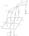
触摸屏220可包括触摸感测电路,该触摸感测电路可包括具有多个电隔离的触摸节点电极222的电容式感测介质(例如,像素化的自电容触摸屏)。触摸节点电极222可耦接到触摸控制器206中的感测信道208,可由通过驱动/感测接口225的来自感测信道的激励信号驱动,并且还可由感测信道通过驱动/感测接口而被感测到,如上所述。在触摸屏220被视为捕获触摸的“图像”(如“触摸图像”)时,将用于检测触摸的导电板(即,触摸节点电极222)标记为“触摸节点”电极可能尤其有用。换句话讲,在触摸控制器206确定在触摸屏220中的每个触摸节点电极222处检测的触摸量之后,可将触摸屏中发生触摸的触摸节点电极的图案视为触摸图像 (例如,触摸触摸屏的手指的图案)。The
计算系统200还可包括用于从触摸处理器202接收输出并基于输出来执行动作的主机处理器228。例如,主机处理器228可连接到程序存储装置 232和显示器、控制器诸如LCD驱动器234。LCD驱动器234可在选择 (栅极)线上向每个像素晶体管提供电压,并可沿数据线向这些相同的晶体管提供数据信号,以控制像素显示图像,如下文更加详细所述的。主机处理器228可使用LCD驱动器234来在触摸屏220上生成显示图像诸如用户界面(UI)显示图像,并可使用触摸处理器202和触摸控制器206来检测触摸屏220上或附近的触摸。触摸输入可由被存储在程序存储装置232中的计算机程序用于执行动作,该动作可包括但不限于移动对象诸如光标或指针、滚动或平移、调节控制设置、打开文件或文档、查看菜单、作出选择、执行指令、操作连接到主机设备的外围设备、应答电话呼叫、拨打电话呼叫、终止电话呼叫、改变音量或音频设置、存储与电话通信相关的信息(诸如地址、频繁拨打的号码、已接来电、未接来电)、登录到计算机或计算机网络上、允许经授权的个体访问计算机或计算机网络的受限区域、加载与用户优选的计算机桌面的布置相关联的用户配置文件、允许访问网页内容、启动特定程序、对消息加密或解密等等。主机处理器228还可执行可能与触摸处理不相关的附加功能。
需注意,如上所述的功能中的一种或多种功能,包括电极和感测信道的配置和操作,可由被存储在存储器(例如图2中的外围设备204之一) 中并由触摸处理器202执行的、或被存储在程序存储装置232中并由主机处理器228执行的固件来执行。该固件也可在任何非暂态计算机可读存储介质内存储和/或输送,以供指令执行系统、装置或设备诸如基于计算机的系统、包括处理器的系统或可从指令执行系统、装置或设备获取指令并执行指令的其他系统使用或与其结合。在本文档的上下文中,“非暂态计算机可读存储介质”可以是可包含或存储程序以供指令执行系统、装置和设备使用或与其结合的任何介质(不包括信号)。计算机可读存储介质可包括但不限于电子、磁性、光学、电磁、红外或半导体系统、装置或设备,便携式计算机磁盘(磁性)、随机存取存储器(RAM)(磁性)、只读存储器(ROM)(磁性)、可擦除可编程只读存储器(EPROM)(磁性)、便携式光盘诸如CD、CD-R、CD-RW、DVD、DVD-R或DVD-RW,或闪存存储器诸如紧凑型闪存卡、安全数字卡、USB存储设备、记忆棒等。Note that one or more of the functions described above, including the configuration and operation of electrodes and sensing channels, may be stored in memory (eg, one of
该固件也可传播于任何传输介质内以供指令执行系统、装置或设备,诸如基于计算机的系统、包含处理器的系统,或从可指令执行系统、装置或设备获取指令并执行指令的其他系统使用或与其结合。在本文的上下文中,“传输介质”可以是可传送、传播或传输程序以供指令执行系统、装置或设备使用或与其结合的任何介质。传输介质可包括但不限于电子、磁性、光学、电磁或红外有线或无线传播介质。The firmware may also be propagated within any transmission medium for an instruction execution system, apparatus or device, such as a computer-based system, a system including a processor, or other system that obtains and executes instructions from an instruction-executable system, apparatus or device used or combined with it. In the context of this document, a "transmission medium" can be any medium that can convey, propagate, or transport a program for use by or in connection with an instruction execution system, apparatus, or device. Transmission media may include, but are not limited to, electronic, magnetic, optical, electromagnetic or infrared wired or wireless propagation media.
图3示出了根据本公开的示例的与自电容触摸节点电极302和感测电路314对应的示例性触摸传感器电路300。触摸节点电极302可对应于触摸节点电极222。触摸节点电极302可具有到与其相关联的接地部的固有自电容,并且具有到仅在对象(诸如手指305)接近或接触电极时才形成的对接地部的附加自电容。触摸节点电极302对接地部的总自电容可被示为电容 304。触摸节点电极302可耦接到感测电路314(其可对应于感测信道 208)。尽管可采用其他配置,但是感测电路314可包括运算放大器308、反馈电阻器312、反馈电容器310和输入电压源306。例如,反馈电阻器312可由开关式电容器电阻器来代替,以使得可由可变反馈电阻器所导致的寄生电容效应最小化。触摸节点电极302可耦接至运算放大器308的反相输入端(-)。AC电压源306(Vac)可耦接至运算放大器308的同相输入端(+)。触摸传感器电路300可被配置为感测由手指或对象触摸或接近触摸传感器面板所引起的触摸节点电极302的总自电容304的变化。输出320可由处理器(例如,触摸控制器206)用于确定接近事件或触摸事件的存在,或者该输出可被输入到离散逻辑网络中,以确定触摸事件或接近事件的存在。应当理解,本公开中所使用的“触摸事件”可包括手指或对象触摸触摸传感器面板(即,与触摸传感器面板物理接触),以及手指或对象接近但不接触所述触摸传感器面板(例如,悬停在触摸传感器面板上方)。FIG. 3 illustrates an example
重新参考图2,在一些示例中,触摸屏220可以是集成式触摸屏,其中触摸感测系统的触摸感测电路元件可被集成到显示器的显示器像素层叠结构中。触摸屏220中的电路元件可包括例如可存在于LCD或其他显示器中的元件,诸如一个或多个像素晶体管(例如,薄膜晶体管(TFT))、栅极线、数据线、像素电极和公共电极。在给定的显示器像素中,像素电极和公共电极之间的电压可控制显示器像素的亮度。像素电极上的电压可由数据线通过像素晶体管提供,该像素晶体管可由栅极线控制。需要指出的是,电路元件不限于整个电路部件,诸如整个电容器、整个晶体管等,而是可包括电路的部分,例如平行板电容器的两个板中的一个板。图4示出了一种示例性配置,其中公共电极402可形成触摸感测系统的触摸感测电路的部分-在本公开的一些示例中,公共电极可形成用于检测触摸屏400上的触摸图像的触摸节点电极,如上所述。每个公共电极402(即,触摸节点电极)可包括多个显示器像素401(被示为具有虚线边界的小正方形),并且每个显示器像素401可包括公共电极402的一部分,其可以是一些类型的LCD或其他显示器的显示器像素的显示器像素层叠结构(即,形成显示器像素的层叠材料层)中的显示系统电路的电路元件-换句话说,公共电极可作为显示系统的一部分来操作,以在触摸屏400上显示显示图像。Referring back to FIG. 2, in some examples, the
在图4所示的示例中,每个公共电极402可用作多功能电路元件,其可作为触摸屏400的显示系统的显示电路来操作,并且还可作为触摸感测系统的触摸感测电路来操作。在该示例中,如上所述,每个公共电极402 可作为触摸屏400的显示电路的公共电极来操作,并且还可作为触摸屏的触摸感测电路来操作。例如,在触摸感测阶段期间,公共电极402可作为触摸感测电路的触摸节点电极的电容部分来操作。触摸屏400的其他电路元件可通过例如开关电连接等方式来形成触摸感测电路的一部分。更具体地,在一些示例中,在触摸感测阶段期间,栅极线可连接到电源诸如电荷泵,其可施加电压以将被包括在触摸节点电极中的显示器像素中的TFT保持在“关闭”状态。激励信号可被施加至公共电极402。如前所述,可通过运算放大器来感测公共电极402的总自电容的变化。公共电极402的总自电容的变化可取决于触摸对象(诸如手指305)与公共电极的接近程度。以这种方式,所测量的公共电极402的总电容的变化,可为触摸屏上或附近的触摸提供指示。In the example shown in FIG. 4, each
通常,触摸感测电路元件中的每个触摸感测电路元件可以是多功能电路元件,其可形成触摸感测电路的一部分并且可执行一项或多项其他功能诸如形成显示电路的一部分,或者该每个触摸感测电路元件可以是仅可作为触摸感应电路来操作的单功能电路元件。类似地,显示电路元件中的每个显示电路元件可以是多功能电路元件,其可作为显示电路来操作并且可执行一项或多项其他功能诸如作为触摸感测电路来操作,或者该每个显示电路元件可以是仅可作为显示电路来操作的单功能电路元件。因此,在一些示例中,显示器像素层叠结构中的一些电路元件可以是多功能电路元件,而其他电路元件可以是单功能电路元件。在其他示例中,显示器像素层叠结构的所有电路元件可以是单功能电路元件。Typically, each of the touch-sensing circuit elements may be a multi-function circuit element that may form part of a touch-sensing circuit and may perform one or more other functions such as forming part of a display circuit, or The each touch sensing circuit element may be a single function circuit element operable only as a touch sensing circuit. Similarly, each of the display circuit elements can be a multifunction circuit element that can operate as a display circuit and can perform one or more other functions such as operating as a touch sensing circuit, or the The display circuit element may be a single-function circuit element that can only operate as a display circuit. Thus, in some examples, some circuit elements in a display pixel stack-up may be multi-function circuit elements, while other circuit elements may be single-function circuit elements. In other examples, all circuit elements of the display pixel stack may be single-function circuit elements.
此外,尽管这里的示例可将显示电路描述成在显示阶段期间进行操作并将触摸感测电路描述成在触摸感测阶段期间进行操作,但应当理解,显示阶段和触摸感测阶段可同时进行操作,例如部分或完全交叠,或者显示阶段和触摸感测阶段可在不同时间进行操作。而且,尽管这里的示例将特定电路元件描述成多功能的并且其他电路元件是单功能的,但应当理解,在其他示例中电路元件不限于特定功能。换言之,在本文的一个示例中被描述为单功能电路的电路元件可在其他示例中被配置为多功能电路,并且反之亦然。Furthermore, although examples herein may describe the display circuit as operating during the display phase and the touch sensing circuit as operating during the touch sensing phase, it should be understood that the display phase and the touch sensing phase may operate simultaneously , eg partially or completely overlapping, or the display phase and touch sensing phase may operate at different times. Furthermore, although the examples herein describe certain circuit elements as being multifunctional and other circuit elements being single function, it should be understood that in other examples the circuit elements are not limited to the particular function. In other words, circuit elements described as single-function circuits in one example herein may be configured as multi-function circuits in other examples, and vice versa.
图4的公共电极402(即,触摸节点电极)和显示器像素401被示为触摸屏400上的矩形或正方形区域。然而,应当理解,公共电极402和显示器像素401不限于所示的形状、取向和位置,而是可包括根据本公开的示例的任何合适的构型。Common electrodes 402 (ie, touch node electrodes) and display
虽然本公开着重讨论的是触摸屏,但是应当理解,本发明的一部分或所有示例可类似地在触摸传感器面板(即,具有不含显示电路的触摸感测电路的面板)中实现。然而,为了简明起见,本发明的示例已并且将在触摸屏的上下文中描述。While this disclosure focuses on touchscreens, it should be understood that some or all examples of the present invention may similarly be implemented in touch sensor panels (ie, panels having touch sensing circuitry without display circuitry). However, for the sake of brevity, examples of the present invention have been and will be described in the context of a touch screen.
水排斥water repelling
在自电容触摸屏中,由自电容触摸节点电极所见的电容可影响在该触摸节点电极处测量的总自电容,并且因此影响该触摸节点电极处的触摸测量。因此,在一些示例中,为了减少或消除可能促成触摸节点电极处测量到的总自电容的不必要的电容,使触摸屏“自举”可以是有益的。使触摸屏“自举”可能需要以与用于驱动和感测触摸节点电极相同频率和相位的电压来驱动触摸屏的一个或多个部件或部分(如上所述),使得可存在于触摸节点电极与触摸屏的一个或多个部分之间的电容可有效地得到消除。例如,使触摸屏自举可能需要以与用于驱动和感测触摸节点电极相同频率和相位的电压来驱动触摸屏的一个或多个栅极线。同样有益的是能够将触摸屏上可能存在的水(例如,水滴)与手指触摸活动区分开来,前者可被忽略,而后者可被处理为触摸活动。应当注意,虽然在自举式触摸屏的上下文中描述了本发明的水检测和水排斥示例,但是水检测和水排斥方案可类似地应用于触摸传感器面板(而不仅仅是触摸屏),该触摸传感器面板中未发生自举,但触摸节点电极会按如下所述的方式被驱动、感测和/或接地。In a self-capacitance touch screen, the capacitance seen by a self-capacitance touch node electrode can affect the total self-capacitance measured at that touch node electrode, and thus the touch measurement at that touch node electrode. Thus, in some examples, it may be beneficial to "bootstrap" the touch screen in order to reduce or eliminate unnecessary capacitance that may contribute to the total self-capacitance measured at the touch node electrodes. "bootstrapping" the touchscreen may require driving one or more components or portions of the touchscreen (as described above) with the same frequency and phase voltages used to drive and sense the touch node electrodes, so that there may be a difference between the touch node electrodes and the touch node electrodes. Capacitance between one or more parts of the touch screen can be effectively eliminated. For example, bootstrapping the touch screen may require driving one or more gate lines of the touch screen with the same frequency and phase voltages used to drive and sense the touch node electrodes. It would also be beneficial to be able to distinguish the possible presence of water (eg, water droplets) on the touch screen from finger touch activity, which can be ignored and which can be treated as touch activity. It should be noted that although the water detection and water rejection example of the present invention is described in the context of a bootstrapped touch screen, the water detection and water rejection scheme can be similarly applied to touch sensor panels (rather than just touch screens), which No bootstrapping occurs in the panel, but the touch node electrodes are driven, sensed and/or grounded as described below.
图5A示出了示例性完全自举式触摸屏500,其中每个触摸节点电极可被同时驱动和感测。触摸屏500可包括触摸节点电极502,504,506和508。触摸节点电极502,504,506和508可以是可被包括在触摸屏500中的触摸节点电极的一部分。为了便于描述,将其他触摸节点电极省去,但是应当理解,本公开的范围包括具有多于四个触摸节点电极的触摸屏。在一些示例中,触摸屏上的所有触摸节点电极可按完全自举配置被同时驱动和感测。在一些示例中,可按完全自举配置并且一部分一部分地对触摸屏进行感测 (例如,一次感测触摸屏的25%,类似于参考图10B所描述的那样),其中所感测的那部分触摸屏中的所有触摸节点电极可被同时驱动和感测(例如,按完全自举配置),随后可按完全自举配置顺序地对触摸屏的剩余部分类似地进行感测,直到整个触摸屏已被感测。在一些示例中,触摸屏的在完全自举配置下当前未被感测的那些部分中的触摸节点电极,可在偏置电压(AC或DC)下发生偏压,或者可利用与下述激励信号相同的激励信号来驱动:用于驱动和感测触摸屏的在完全自举配置下当前正被感测的那部分中的触摸节点电极的激励信号。FIG. 5A shows an exemplary fully bootstrapped
触摸节点电极502,504,506和508中的每个可被来自激励源514的同一激励信号同时(或在驱动时被顺次地感测)驱动和感测(由“DS”表示),该激励源可耦接到可包括触摸屏500的设备(例如,图1A-图1C中所示的任何设备)的系统接地部516。激励源514可对应于图3中的感测电路314和/或电压源306。虽然触摸节点电极502,504,506和508被示出为耦接到相同的激励源514,但是应当理解,如果触摸节点电极耦接到提供相同激励信号的不同激励源的任何组合,则可获取基本上相同的结果。由于触摸节点电极502,504,506和508中的每一个触摸节点电极可利用同一激励信号而被同时驱动和感测(或在驱动时被顺次地感测),因此可能存在于触摸节点电极之间的电容可得到有效地消除,并且所感测的触摸节点电极的总自电容可被限制为可存在于触摸节点电极和手指(或对象)518之间的电容,以及可能存在于触摸节点电极和其他系统部件(例如,系统接地部)之间的其他潜在电容(例如,寄生电容)。这些电容可由C1 503、C2 505、C3 507和C4 509表示。Each of
如图5A所示,Cg 520可表示手指518和系统接地部之间的总电容,并且可以是各种电容的组合,如下所述。具体地,手指518可在其自身和大地之间具有电容C人体,其中C人体可表示例如人体到大地的电容。手指518 还可在其自身与可包括触摸屏500的设备之间具有电容CF-SG,其中CF-SG可表示手指到系统(设备)接地部的电容。包括触摸屏500的设备可在其自身与大地之间具有电容CSG-EG,其中CSG-EG可表示系统(设备)接地部到大地的电容。在一些示例中,C人体可比CF-SG和CSG-EG大得多。因此,可认为手指518有效地通过C人体短接到大地。因此,可认为CSG-EG在系统(设备)接地部与手指518(可以短接到地面)之间;而从前文可知,CF-SG可以是系统(设备)接地部和手指518之间的另一电容。CF-SG和CSG-EG故而可以是能够存在于手指518和系统接地部516之间的并联电容。这样,手指518和系统接地部之间的总电容Cg 520可被表示为:As shown in FIG. 5A, Cg 520 may represent the total capacitance between
Cg=CF-SG+CSG-EG (1)C g = C F-SG + C SG-EG (1)
来自触摸节点电极502,504,506和508的电流可流过手指518和Cg 520 并流至系统接地部516。然而,由于与Cg 520相关联的阻抗可至少部分地将手指518与系统接地部516隔离,因此当更多的电流从触摸节点电极 502,504,506和508流过手指518并流至系统接地部516时,手指518处的电压可移动得与系统接地部516的差距越来越大。由于触摸节点电极502,504,506和508中的每个触摸节点电极可被同时驱动和感测,因此来自全部四个触摸节点电极的电流均可流过手指518并流至系统接地部516。其结果是,手指518处的电压相对于系统接地部而言可以相对较高,并且C1 503、C2 505、C3 507和C4 509中的每一者两端的电压降可相对更小,这可导致电荷耦合减少,并且导致在与电容C1、C2、C3和C4相关联的每个触摸节点电极处感测到的电容发生衰减。该衰减可反映在衰减因子中,C1 503、 C2 505、C3507和C4 509电容均可与该衰减因子相乘,其可表示为:Current from
α=Cg/C总 (2)α=Cg/ Ctotal ( 2)
其中α可表示衰减因子,并且:where α can represent the decay factor, and:
C总=Cg+C1+C2+C3+C4 (3)C total = C g + C 1 + C 2 + C 3 + C 4 (3)
因此,在任一触摸节点电极处感测到的有效自电容可表示为:Therefore, the effective self-capacitance sensed at any touch node electrode can be expressed as:
C有效,X=α*CX (4)C is valid, X = α*C X (4)
其中CX可以是C1 503、C2 505、C3 507或C4 509。所感测到的触摸节点电极的自电容发生的这种衰减可使得感测触摸屏500上的触摸变得困难。在一些示例中,触摸屏500包括全部被同时驱动和感测的更多个触摸节点电极,并且用户手部(或其他对象)的许多部分接近/接触触摸屏(例如,用户的手掌、拇指和多根手指接触所述触摸屏),此时衰减因子α可低至 4%。应当理解,在一些示例中,手指518可良好接地,在这种情况下,Cg可非常大(或者可以说是无穷大的),并且α可约为1(即,不衰减)。在手指518未接地的情况下,由于触摸信号衰减程度非常大,因此可能难以检测到触摸。在一些示例中,可通过部分地而不是完全地使触摸屏自举来减少可呈现出的触摸信号衰减量。Wherein C X can be
图5B示出了其中仅一部分触摸节点电极可在给定时刻被驱动和感测的示例性部分自举式触摸屏501。触摸屏501可与触摸屏500大致相同,不同之处在于,在触摸屏500中,触摸节点电极502,504,506和508全部被同时驱动和感测,而在触摸屏501中,仅触摸节点电极502(触摸节点电极 DS)可被驱动和感测。触摸节点电极504和506(触摸节点电极D)可被驱动但不被感测,并且触摸节点电极508(触摸节点电极G)可被接地到系统接地部516。虽然为了清楚起见而未示出,但是触摸节点电极504和506 可耦接到激励源,以便由正在驱动触摸节点电极502的同一激励信号来驱动。另外,应当理解,在触摸节点电极个数比图5B所示更多的触摸屏中,根据本公开的示例,DS、D和G触摸节点电极图案可在触摸屏的一部分上或整个触摸屏上重复。此外,在一些示例中,触摸屏的部分自举扫描可包括,至少一个触摸节点电极被驱动和感测,并且至少一个触摸节点电极接地,剩余触摸节点电极可被驱动和感测、仅被驱动、接地、浮接或处于任何其他电气状态。FIG. 5B shows an exemplary partially bootstrapped
部分自举式触摸屏501可表现出完全自举式触摸屏500的许多益处。具体地,由于触摸节点电极502,504和506可利用同一激励信号来驱动,因此触摸节点电极502(目标触摸节点电极,即总自电容受到感测的触摸节点电极)与触摸节点电极504和506之间的电容可继续有效地得到消除。触摸节点电极502与触摸节点电极508之间的电容可能不会得到消除,这是由于触摸节点电极508可耦接到系统接地部516;然而,由于触摸节点电极 502和508可相对于彼此对角地设置(尽管应当理解,它们不一定要这样设置),这两者之间可能存在的电容可相对较小。因此,在触摸节点电极502 处感测到的总自电容,可基本上不含可能存在于触摸节点电极502和其他触摸节点电极之间的电容,这可是完全自举式触摸屏的一个益处。A partially bootstrapped
与完全自举式触摸屏500相比,部分自举式触摸屏501也可表现出较少的触摸信号衰减。而在触摸屏500中,从触摸节点电极到接地部的唯一电流路径可流过手指518和Cg520,而在触摸屏501中,从触摸节点电极到接地部的电流可流过C4 509并流至系统接地部516,也可流过手指518 和Cg 520。因此,手指518处的电压可降至更靠近系统接地部516,这可能导致C1 503两端的电压降比触摸屏500中更多;这样,可在触摸节点电极 502处感测到C1 503的更多的电荷耦合和较少的衰减。部分自举式触摸屏衰减因子可被表示为:Partially bootstrapped
α=(Cg+C4)/C总 (5)α=(C g +C 4 )/ Ctotal (5)
与前文类似,在触摸节点电极502处感测到的有效自电容可被表示为:Similar to the previous, the effective self-capacitance sensed at the
C有效,1=α*C1 (6)C is valid, 1 = α*C 1 (6)
在触摸屏501包括更多个的触摸节点电极的示例中,这些触摸节点电极在所示的部分自举模式中被驱动、感测并接地,同时用户手部的许多部分接近/接触所述触摸屏(例如,用户的手掌、拇指和多根手指接触所述触摸屏),在这种情况下,衰减系数可从完全自举式触摸屏中的~4%增加到部分自举式触摸屏中的~25%。这种增加可由可包括在等式(5)的分子中的C4附加项导致,并且与触摸屏500相比,可使触摸屏感测电路的信噪比要求放宽多于六倍,这可降低在触摸屏上感测触摸的难度。In the example where
如上所述,在一些示例中,水或水滴可能存在于本公开的触摸屏上。能够区分存在水的情况与存在手指的情况对于确保适当的触摸屏操作来说是有益的。As mentioned above, in some examples, water or water droplets may be present on the touch screen of the present disclosure. Being able to distinguish between the presence of water and the presence of a finger is beneficial to ensure proper touch screen operation.
图6A示出了根据本公开的示例的其上可驻留有孤立水滴619的示例性完全自举式触摸屏600。触摸屏600可基本上类似于图5A中的触摸屏 500,不同之处在于手指518可被孤立水滴619替代。孤立水滴619可以是可驻留在触摸屏600表面上的水滴,并且可以是“孤立的”,由于它可能不触摸用户、用户的手指或可至少部分接地的任何其他对象。如在触摸屏500中的那样,触摸屏600可以是完全自举的。6A illustrates an exemplary fully bootstrapped
由于孤立水滴619可与接地部隔离,因此从水滴到接地部不会存在路径,故而没有电流可从触摸节点电极602,604,606和608流过该孤立水滴到达接地部。其结果是,孤立水滴619可使触摸节点电极602,604,606和608 中的任一触摸节点电极的自电容基本上不发生变化,因此孤立水滴不会带来其自身的自电容触摸图像。换句话说,对于完全自举式触摸屏而言,水滴可被自动忽略/从触摸扫描中弃去。Since the
然而,由于上述原因,有时本公开的触摸屏可按部分自举配置进行操作。图6B示出了根据本公开的示例的其上可驻留有孤立水滴619的示例性部分自举式触摸屏601。触摸屏601可基本上类似于图5B中的触摸屏 501,不同之处在于手指518可被孤立水滴619替代,如图6A的那样。与图6A所示不同的是,由于触摸屏601可被部分自举,因此可存在从水滴 619到接地部的路径。具体地,水滴619可通过C4 609和触摸节点电极608 而被耦接到接地部616。其结果是,电流可从触摸节点电极602,604和606 流过水滴619到达接地部616。因此,在部分自举式触摸屏601上获取的自电容触摸图像中可能出现水滴619。However, for the reasons described above, sometimes the touch screen of the present disclosure may operate in a partial bootstrap configuration. 6B illustrates an exemplary partially bootstrapped
出于上文结合图5B所述的类似原因,与水滴619相关联的衰减因子可被表示为:For similar reasons described above in connection with Figure 5B, the attenuation factor associated with
α=C4/C总 (7)α = C 4 /C total (7)
与前文类似,在触摸节点电极602处感测到的有效自电容可被表示为:Similar to the previous, the effective self-capacitance sensed at the
C有效,1=α*C1 (8)C is valid, 1 = α*C 1 (8)
因此,在部分自举配置中,在触摸屏601上可检测到水滴619的衰减的自电容触摸图像。Thus, in a partially bootstrapped configuration, a decaying self-capacitance touch image of
在一些示例中,本公开的触摸屏可另外地或替代地以互电容配置来操作。在一些示例中,触摸屏可按互电容配置操作,以便校正与未接地(或接地不良)用户相关联的上述衰减,并且在一些示例中,触摸屏可作为将水从实际触摸活动区分开并排斥的一部分按相互电容配置进行操作,如本文将描述的。本公开的后文将对未接地的用户衰减校正进行讨论。图6C示出了根据本公开的示例的以互电容配置操作的其上可驻留有孤立水滴619 的示例性触摸屏650。所示的互电容驱动和感测方案可在上述完全/部分自举方案之前、之后或之中使用,如本文稍后将要更详细描述的,另外,图 6C的示例性互电容驱动和感测方案图示出,该方案应用于四个触摸节点电极,但是应当理解,该方案可类似地扩展到可能存在于本公开的触摸屏上的附加触摸节点电极。例如,触摸屏上的一组四个触摸节点电极可如下所述被驱动、感测和接地。在一些示例中,该组四个触摸节点电极可被依次驱动、感测和接地,即一次一个。在一些示例中,该组四个触摸节点电极可被至少部分同时地驱动、感测和接地,即每次多于一个。In some examples, the touchscreens of the present disclosure may additionally or alternatively operate in a mutual capacitance configuration. In some examples, the touch screen may operate in a mutual capacitance configuration in order to correct for the aforementioned attenuation associated with an ungrounded (or poorly grounded) user, and in some examples, the touch screen may act as a means of distinguishing and repelling water from actual touch activity Some operate in a mutual capacitance configuration, as will be described herein. Ungrounded user attenuation correction is discussed later in this disclosure. 6C illustrates an
现在将描述互电容驱动和感测方案。在第一相互电容扫描时间段内,触摸屏的触摸节点电极可被驱动和感测,如图6C所示。具体地说,可经由激励源617驱动左上方的触摸节点电极602(D触摸节点电极)。激励源 617可以是用于向触摸节点电极602提供电压的任何适当的电压源。可经由读出放大器620来感测右下方的触摸节点电极608(S触摸节点电极)(例如,D触摸节点电极602和S触摸节点电极608可对角地布置)。右上方和左下方的触摸电极604和606(G触摸节点电极)可接地(或在另一个基准电压下发生偏压)。触摸节点电极的上述配置可允许D触摸节点电极 602和S触摸节点电极608之间的互电容分别被测量。在一些示例中,可通过如下方式来获取互电容测量:利用一个或多个激励缓冲器来激励触摸屏上的一个或多个D触摸节点电极,利用一个或多个AC接地缓冲器来将一个或多个G触摸节点电极接地,和/或利用一个或多个读出放大器(例如,感测电路)来感测一个或多个S个触摸节点电极。用于使触摸节点电极被驱动、感测和/或接地的机制可类似于先前描述的方案(例如,就图5A-图 5B和图6A-图6B而言)和/或其他等效方案,为了简明起见,本文不再重复其细节。Mutual capacitance drive and sensing schemes will now be described. During the first mutual capacitance scan period, the touch node electrodes of the touch screen may be driven and sensed, as shown in FIG. 6C . Specifically, the upper left touch node electrode 602 (D touch node electrode) can be driven via the
在一些示例中,可在第二互电容扫描时间段内执行第二互电容扫描。在第二互电容扫描时间段内,可驱动和感测触摸节点电极,使得右上方的触摸节点电极可被驱动,左下方的触摸节点电极可被感测,并且左上方和右下方的触摸节点电极可接地。在经过两个互电容扫描时间段之后,可以获取触摸屏上每对对角的触摸节点电极之间的互电容测量。应当理解,可利用其他驱动和感测配置来获取本公开的示例的互电容测量,并且所提供的配置仅仅是一个示例。例如,在图6C中,替代驱动左上方的触摸节点电极并感测右下方的触摸节点电极,可驱动右下方的触摸节点电极并且可感测左上方的触摸节点电极,以获取基本上相同的结果。应当理解,本公开中所使用的“互电容”可指触摸屏上的多个部件之间(例如,D和S触摸节点电极之间)所示出的标称电容,或者在适当的情况下是指在触摸屏的多个部件之间所示出的标称电容变化。In some examples, the second mutual capacitance scan may be performed during the second mutual capacitance scan period. During the second mutual capacitance scan period, the touch node electrodes may be driven and sensed such that the upper right touch node electrode may be driven, the lower left touch node electrode may be sensed, and the upper left and lower right touch nodes The electrodes can be grounded. Mutual capacitance measurements between each pair of diagonal touch node electrodes on the touch screen can be acquired after two mutual capacitance scanning periods. It should be appreciated that other drive and sense configurations may be utilized to obtain mutual capacitance measurements of examples of the present disclosure, and that the configuration provided is only one example. For example, in Figure 6C, instead of driving the upper left touch node electrode and sensing the lower right touch node electrode, the lower right touch node electrode may be driven and the upper left touch node electrode may be sensed to obtain substantially the same result. It should be understood that "mutual capacitance" as used in this disclosure may refer to the nominal capacitance shown between various components on the touch screen (eg, between the D and S touch node electrodes), or as appropriate Refers to the nominal capacitance variation shown between components of a touch screen.
图6C还示出了与本公开的互电容驱动和感测方案相关联的各种电容。水滴619可在其自身与触摸节点电极602之间具有电容C1 603,在其自身与触摸节点电极604之间具有电容C2 605,在其自身与触摸节点电极606 之间具有电容C3 607,并且在其自身与触摸节点电极608之间具有电容C4 609。当驱动一个触摸节点电极并感测另一个触摸节点电极时,可感测到贯水滴619互电容。例如,可感测到从触摸节点电极602通过C1 603到达水滴619再通过电容C4 608到达触摸节点电极608的互电容。触摸节点电极 602和608之间的贯水滴619互电容可被表示为:Figure 6C also shows various capacitances associated with the mutual capacitance drive and sense scheme of the present disclosure.
CM-水=(C1*C4)/(C1+C2+C3+C4) (9)C M-water = (C 1 *C 4 )/(C 1 +C 2 +C 3 +C 4 ) (9)
因此,在本公开的触摸屏的互电容测量中,水滴619可显现出来。尽管未示出,但手指或其他对象(无论是部分接地还是完全接地的)都可类似地出现在本公开的触摸屏的互电容测量中。触摸节点电极602和608之间的贯指(或对象)互电容可被表示为:Therefore, in the mutual capacitance measurement of the touch screen of the present disclosure, the
CM-手指=(C1*C4)/(Cg+C1+C2+C3+C4) (10)C M-finger =(C 1 *C 4 )/(C g +C 1 +C 2 +C 3 +C 4 ) (10)
其中Cg可表示手指和系统接地部之间的总电容,如先前结合图5A-图5B所讨论的那样。where Cg may represent the total capacitance between the finger and system ground, as previously discussed in connection with Figures 5A-5B.
可使用任何适当的电路来将本公开的触摸屏的触摸节点驱动、感测和/ 或接地。图7A示出了具有耦接到适当电路的触摸节点的部分自举式触摸屏 700的示例性配置-即,可与类似的适当电路一起操作的完全自举式和/或互电容配置。触摸屏700可与触摸屏501和601基本上相同。可被驱动和感测的触摸节点702可耦接到感测电路714。感测电路714可对应于例如图3 中的感测电路314。可被驱动但不被感测的触摸节点704和706可耦接到激励缓冲器716。在一些示例中,感测电路714和激励缓冲器716可共享激励源720,这是由于触摸节点702,704和706可由同一激励信号驱动;然而,应当理解,感测电路和激励缓冲器不一定要共享同一激励源。可接地的触摸节点708可耦接到AC接地缓冲器718。电压源722可向AC接地部提供由AC接地缓冲器718提供的DC偏压。在一些示例中,感测电路714、激励缓冲器716和/或AC接地缓冲器718可被包括在触摸控制器206中,并且在一些示例中,被被包括在感测信道208中。此外,感测电路714、激励缓冲器716和/或AC接地缓冲器718仅作为示例而提供,并且应当理解,可使用其他电路来类似地将本公开的触摸节点驱动、感测和接地。The touch nodes of the touch screen of the present disclosure may be driven, sensed, and/or grounded using any suitable circuitry. Figure 7A shows an exemplary configuration of a partially bootstrapped
图7B示出了可利用开关阵列752将适当的电路耦接到触摸节点的部分自举式触摸屏750的示例性配置。触摸屏750中的触摸节点可耦接到开关阵列752。开关阵列752可包括可将输入端耦接到开关阵列的一个或多个输出端的开关和/或多路复用器或其他电路。开关阵列752可耦接到放大器电路754,该放大器电路可包括电路诸如图7A所示的一个或多个感测电路 714、一个或多个激励缓冲器716和一个或多个AC接地缓冲器718。放大器电路部分754可耦接到触摸处理电路756,诸如模拟前端(AFE)、模数转换器(ADC)和用于处理在触摸屏750上检测到的触摸信号的解调电路。FIG. 7B shows an exemplary configuration of a partially bootstrapped
电路诸如感测电路714、激励缓冲器716和AC接地缓冲器718不需要永久地耦接到触摸节点来进行适当的触摸屏操作。相反,此类电路可通过开关阵列752耦接到触摸节点,使得适当的触摸节点可仅在需要时耦接到适当的电路。这可允许多个触摸节点共享公共电路,继而可减少触摸屏操作所需的电路的数量。例如,可使用开关阵列752来将要驱动和感测的第一触摸节点(第一DS触摸节点)耦接到感测电路714。当要驱动和感测第二触摸节点(第二DS触摸节点)时,开关阵列可将同一感测电路714耦接到第二触摸节点,以驱动和感测第二触摸节点而不是第一触摸节点。此类开关阵列752的操作可类似地应用于将激励缓冲器716、AC接地缓冲器 718以及任何其他适当的电路耦合至适当的触摸节点。开关阵列752可以是可将触摸节点耦接到放大器电路部分754中的适当电路的任何合适的开关网络。Circuits such as
在一些示例中,触摸屏750上的触摸节点可在单个激励配置中被激励,如本公开中普遍描述的那样(例如,放大器电路部分754中的单个感测电路714可在任何时刻激励和感测单个触摸节点)。在一些示例中,本公开的触摸屏扫描可扩展到多激励型具体实施,其中触摸屏750上的触摸节点可按多激励配置被激励(例如,放大器电路部分754中的单个感测电路714可在任何时刻激励和感测多个触摸节点)。在多激励配置中,可使用任何合适的多激励方案,并且可酌情使用开关阵列752来实现多激励方案。例如,可利用具有接收侧编码的哈达玛(Hadamard)/循环矩阵驱动和感测方案,其中除了共模触摸扫描步骤之外,对于每个触摸扫描步骤,接收正相位激励信号的触摸节点和接收负相位激励信号的触摸节点可为等同的。In some examples, touch nodes on
如图5B、图6B和图7A所示,在部分自举扫描配置中,在任何一个时刻,每四个触摸节点中仅有一个触摸节点可被驱动和感测。因此,可仅捕获总自电容触摸图像的四分之一。另外,如图6C所示,在任何一个时刻,与每四个触摸节点仅一对触摸节点相关联的互电容可被感测。因此,可仅捕获总互电容触摸图像的一半。如此一来,有益的是,在某个时间点将每个触摸节点驱动、感测和/或接地,以便捕获触摸屏上的完整的自电容和/或互电容触摸图像。下面将描述各种自电容和互电容扫描方案。应当注意,本公开的示例可扩展到其他部分自举、完全自举和互电容方案,这些方案中,不同数量以及布置方式的触摸节点可被驱动和感测、被驱动但不被感测、被感测,以及被接地;然而,为了便于描述,本公开的示例将重点聚焦具有四个触摸节点的配置。As shown in Figures 5B, 6B and 7A, in a partial bootstrap scan configuration, only one of every four touch nodes can be driven and sensed at any one time. Therefore, only a quarter of the total self-capacitive touch image can be captured. Additionally, as shown in FIG. 6C, at any one time, the mutual capacitance associated with only one pair of touch nodes for every four touch nodes can be sensed. Therefore, only half of the total mutual capacitance touch image can be captured. As such, it is beneficial to drive, sense and/or ground each touch node at some point in time in order to capture a full self-capacitance and/or mutual-capacitance touch image on the touch screen. Various self-capacitance and mutual-capacitance scanning schemes will be described below. It should be noted that the examples of the present disclosure can be extended to other partial bootstrap, full bootstrap, and mutual capacitance schemes in which different numbers and arrangements of touch nodes can be driven and sensed, driven but not sensed, sensed, and grounded; however, for ease of description, examples of this disclosure will focus on configurations with four touch nodes.
如上所述,本公开的触摸屏上的孤立水滴(即,未接触接地用户或对象的水滴)可能不会出现在触摸屏的完全自举扫描上,但可能不同程度地出现在触摸屏的部分自举扫描和互电容扫描上。因此,可使用触摸屏的完全自举扫描和触摸屏的部分自举和/或互电容扫描的比较结果来识别触摸屏上的水的存在,并将水从可用于分析触摸活动的最终触摸图像中忽略或弃去。应当理解,本公开的水检测和水排斥方案适用于可能存在于触摸屏上的孤立水滴,而不适用于例如可能接触用户手指的水滴。As noted above, isolated water droplets (ie, water droplets that do not contact a grounded user or object) on touchscreens of the present disclosure may not appear on a full bootstrap scan of the touchscreen, but may appear on partial bootstrap scans of the touchscreen to varying degrees and mutual capacitance scan on. Therefore, a comparison of a full bootstrap scan of the touchscreen and a partial bootstrap and/or mutual capacitance scan of the touchscreen can be used to identify the presence of water on the touchscreen and omit water from the final touch image that can be used to analyze touch activity or discard. It should be understood that the water detection and water repelling schemes of the present disclosure are applicable to isolated water droplets that may be present on a touch screen, but not to water droplets that may be in contact with a user's finger, for example.
图8A示出了根据本公开的示例的触摸屏800上的示例性完全自举扫描。图8A所示的完全自举扫描可基本上类似于图5A和图6A所示的完全自举扫描。如上所述,由于进行了所示完全自举扫描(在用户未接地或接地不良的情况下,触摸活动会衰减),触摸屏800上的触摸活动可被感测到,但是水不会被感测到。因此,图8A的完全自举扫描可提供包括触摸活动但不包括水的触摸图像,该触摸图像具有4×4个触摸节点的分辨率(每个触摸节点802可独立地被驱动和感测,无论是同时还是以其他方式)。FIG. 8A shows an exemplary full bootstrap scan on a
图8B示出了根据本公开的示例的触摸屏800上的示例性部分自举扫描。图8B所示的部分自举扫描可基本上类似于图5B和图6B所示的部分自举扫描。在一些示例中,部分自举扫描可在至少四个步骤中进行,在这些步骤期间,一组四个触摸节点中的不同触摸节点802可被驱动和感测、被驱动但不被感测,以及被接地。具体地,在第一步骤804中,左上方的触摸节点802可被驱动和感测,右下方的触摸节点可接地,并且剩下的两个触摸节点(左下方和右上方)可被驱动但不被感测。如图所示,第二步骤806、第三步骤808和第四步骤810步骤可使不同排列方式的触摸节点被驱动和感测、被驱动但不被感测,以及被接地,使得在第四步骤结束时,该组四个触摸节点中的所有触摸节点已在某个时间点被驱动和感测。所提供的扫描步骤的顺序仅是示例性的,并且应当理解,可利用不同的扫描步骤顺序。8B illustrates an exemplary partial bootstrap scan on
如上所述,由于可能存在于触摸屏800上的水可被反映在触摸屏的部分自举扫描中,因此图8B的部分自举扫描可产生包括触摸活动和水的触摸图像,该触摸图像具有4×4个触摸节点的分辨率。可将该触摸图像与图8A 中获取的触摸图像(其可包括触摸活动而不包括水)进行比较,以确定触摸屏800上是否存在水,并确定可能存在水的位置,接着在分析触摸屏上的触摸时,可将触摸图像中与水相关联的那部分弃去或忽略。As described above, since water that may be present on the
在一些示例中,为了节省时间和/或减少资源(例如感测电路)用量,在不需要高分辨率水排斥的情况下(例如,如果不需要在触摸节点电极电平上进行水检测),可针对水检测和水排斥目的来降低触摸屏的完全自举扫描的分辨率。图8C示出了根据本公开的示例的触摸屏800上的分辨率降低的示例性完全自举扫描。在图8C的扫描中,一组四个触摸节点可由同一感测电路驱动和感测,而不是每个触摸节点802单独地被各个感测电路驱动和感测(无论是同时还是以其他方式)。与图8A的扫描相比,由于每次触摸屏有更大的部分可被驱动和感测,因此这可减少所需的感测电路的数量,和/或可减少扫描整个触摸屏800所需的时间量。然而,其结果是,所得到的触摸图像的分辨率可降至2×2个“复合触摸节点”(2×2的触摸节点组)。可将该分辨率降低的触摸图像与例如从图8B的部分自举扫描获取的触摸图像进行比较,从而如前述那样确定触摸屏800上是否存在水,并确定可能存在水的位置,接着在分析触摸屏上的触摸时,可将触摸图像中与水相关联的那部分弃去或忽略,尽管分辨率比以前低。In some examples, to save time and/or reduce resource (eg, sense circuit) usage, where high resolution water rejection is not required (eg, if water detection is not required at the touch node electrode level), The resolution of the full bootstrap scan of the touch screen can be reduced for water detection and water rejection purposes. 8C illustrates an exemplary full bootstrap scan with reduced resolution on
图8A-图8C描述了一种水检测和水排斥方案,其中将完全自举触摸扫描与部分自举触摸扫描进行比较,以确定触摸屏上水的存在和/或位置。在一些示例中,可使用替代的水检测和水排斥方案,该方案可基于完全自举触摸扫描和互电容扫描。8A-8C depict a water detection and water repelling scheme in which a full bootstrap touch scan is compared to a partial bootstrap touch scan to determine the presence and/or location of water on a touch screen. In some examples, alternative water detection and water repulsion schemes may be used, which may be based on fully bootstrapped touch scanning and mutual capacitance scanning.
图9A示出了根据本公开的示例的触摸屏900上的示例性完全自举扫描。图9A的扫描可与图8A的扫描相同,为了简明起见,此处省略其细节。FIG. 9A shows an exemplary full bootstrap scan on a
图9B示出了根据本公开的示例的触摸屏900上的示例性互电容扫描。图9B所示的互电容扫描基本上类似于图6C所示的互电容扫描。在一些示例中,该互电容扫描可在至少两个步骤中进行,在此期间,一组四个触摸节点中的不同触摸节点902可被驱动、感测和接地,如前所述。具体而言,在第一步骤904中,左上方的触摸节点902可被驱动,右下方的触摸节点可被感测,剩下的两个触摸节点(左下方和右上方)可接地。如图所示,第二步骤906可使不同排列方式的触摸节点被驱动、感测和接地,使得在第二步骤结束时,该组四个触摸节点中的两对触摸节点的互电容已在某个时间点被感测。所提供的扫描步骤和具体配置的顺序仅是示例性的,并且应当理解,可利用不同的扫描步骤顺序。FIG. 9B illustrates an example mutual capacitance scan on
如上所述,由于可能存在于触摸屏900上的水可被反映在触摸屏的互电容扫描中,因此图9B的互电容扫描可产生包括触摸活动和水的触摸图像。可将该触摸图像与图9A中获取的触摸图像(其可包括触摸活动而不包括水)进行比较,以确定触摸屏900上是否存在水,并确定可能存在水的位置,接着在分析触摸屏上的触摸时,可将触摸图像中与水相关联的那部分弃去或忽略。As described above, since water that may be present on the
如前所述,在一些示例中,为了节省时间和/或减少资源(例如感测电路)用量,在不需要高分辨率水排斥的情况下(例如,如果不需要在触摸节点电极电平上进行水检测),可针对水检测和水排斥目的来降低触摸屏的完全自举扫描的分辨率。图9C示出了根据本公开的示例的触摸屏900上的分辨率降低的示例性完全自举扫描。图9C的扫描以及所得到的水检测和水排斥方案,可类似于参照图8C所描述的内容,为了简明起见,不再重复其细节。As previously mentioned, in some examples, in order to save time and/or reduce resource (eg, sense circuit) usage, in cases where high-resolution water repellency is not required (eg, if not required at the touch node electrode level) water detection), the resolution of a full bootstrap scan of the touchscreen can be reduced for water detection and water rejection purposes. 9C illustrates an exemplary full bootstrap scan with reduced resolution on
现在将描述各种触摸屏显示帧和触摸帧配置,在这些配置中可采用图 8A-图8C及图9A-图9C的水检测和水排斥方案。所提供的配置仅是示例性的,并且应当理解,可使用基于相似原理的其他配置,并得到相似的结果。Various touch screen display frame and touch frame configurations will now be described in which the water detection and water rejection schemes of FIGS. 8A-8C and 9A-9C may be employed. The provided configurations are exemplary only and it should be understood that other configurations based on similar principles may be used with similar results.
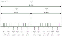
图10A示出了根据本公开的示例的示例性基础触摸屏显示帧和触摸帧配置1000。显示帧1002可是本公开的触摸屏的显示器部分可被更新的持续时间。显示帧1002可包括两个触摸帧,即触摸帧1004和触摸帧1006,在这两个触摸帧期间,可检测触摸屏的所有部分上的触摸活动(例如,可按比更新显示器更快的速度扫描触摸活动-在一些示例中,以两倍的速度)。换句话说,在一些示例中,触摸帧1004可以是可检测触摸屏的所有部分上的触摸活动的第一持续时间,并且触摸帧1006可以是可检测触摸屏的所有部分上的触摸活动的的第二持续时间。显示帧1002与触摸帧1004和1006 的一对二关系仅作为示例提供,并且应当理解,对于图10A的示例以及本公开的所有示例来说,可采用其他比例的显示帧与触摸帧。FIG. 10A illustrates an exemplary base touch screen display frame and
触摸帧1004可包括扫描步骤MC1 1008和MC2 1014。MC1 1008和 MC2 1014可分别对应于图9B中的互电容扫描步骤904和906。如上所述,在一些示例中,可使用MC1 1008和MC2 1014来校正未接地的用户触摸信号的衰减和/或水检测和水排斥。
在触摸帧1004中,MC1 1008和MC2 1014可由PB1 1010和PB2 1012 分隔开。PB11010和PB2 1012可对应于在触摸屏的不同区域中执行的部分自举扫描步骤804,806,808和810。换句话说,PB1 1010可对应于在触摸屏的第一区域中执行的部分自举扫描步骤,并且PB2 1012可对应于在触摸屏的第二区域中执行的部分自举扫描步骤。类似地,PB3 1016和PB4 1018可分别对应于在触摸屏的第三区域和第四区域中执行的部分自举扫描步骤。 PB11010、PB2 1012、PB3 1016和PB4 1018合起来可在触摸屏上提供完整的部分自举触摸图像。将在下文更详细地描述PB1 1010、PB2 1012、PB3 1016和PB4 1018的细节。如上所述,在一些示例中,可使用PB1 1010、 PB2 1012、PB3 1016和PB4 1018来获取触摸屏上的触摸图像,和/或校正未接地的用户触摸信号的衰减。触摸帧1006可与触摸帧1004相同。In
图10B示出了图10A中部分自举扫描步骤的示例性细节。在一些示例中,可通过逐个扫描触摸屏的各个部分而不是一次性地扫描触摸屏的所有部分来减少扫描本公开的触摸屏所需的感测电路的量,如将在下文更详细描述的那样。在PB1 1010期间,可使用部分自举扫描方案来扫描触摸屏的第一部分1011(例如,第一个四分之一)。作为该扫描的一部分,可按图案1020所示的配置来扫描触摸屏的第一部分1011的触摸电极(类似于参照图8C所描述的扫描步骤804,806,808和810)。可按图案1022所示的配置来驱动触摸屏的其余部分,该配置可与图案1020所示的配置相对应。图案1022中的扫描配置可与图案1020中的扫描配置相同,而唯一不同之处在于图案1020中的DS触摸节点电极在图案1022中可被驱动但不被感测 (即,DS触摸节点电极可变为D触摸节点电极)。FIG. 10B shows exemplary details of a portion of the bootstrap scan step in FIG. 10A. In some examples, the amount of sensing circuitry required to scan the touchscreens of the present disclosure may be reduced by scanning portions of the touchscreen individually rather than scanning all portions of the touchscreen at once, as will be described in more detail below. During
扫描步骤PB2 1012、PB3 1016和PB4 1018的细节可类似于PB1 1010 的细节,为了简明起见,将不再重复其细节。PB1 1010、PB2 1012、PB3 1016和PB4 1018合起来可提供整个触摸屏的部分自举触摸图像。可以理解,在一些示例中,可按少于或多于此处呈现的扫描次数来获取整个触摸屏的部分自举触摸图像(例如,可根据图案1020同时扫描整个触摸屏);然而,在给定时间仅扫描触摸屏的一些部分可减少所需的感测电路的量。通常将假设扫描触摸屏的一些部分来提供本公开的示例,但本公开的范围不限于此。Details of
图11A示出了根据本公开的示例的示例性水检测和水排斥显示帧和触摸帧配置1100。类似于前述内容,显示帧1102可包括两个触摸帧1104和 1106。触摸帧1104可基本上类似于图10A中的触摸帧1004,不同之处在于触摸帧1104可以另外包括处于扫描步骤MC11108和MC2 1114之前的扫描步骤FB 1120。FB 1120可对应于如图8A、图8C、图9A或图9C所示的完全自举扫描步骤。PB1 1110、PB2 1112、PB3 1116、PB4 1118、MC1 1108和MC2 1114可对应于图10A中的PB1 1010、PB2 1012、PB3 1016、 PB4 1018、MC1 1008和MC2 1014。FIG. 11A illustrates an exemplary water detection and water repelling display frame and
FB 1120可提供整个触摸屏的完全自举触摸图像。在一些示例中,这种完全自举触摸图像可以是全分辨率(一次性地感测或逐个部分地感测),或者如前所述可以是分辨率降低的,这可应用于本公开所述的一个或多个示例扫描配置。如上所述,可将来自PB1 1110、PB2 1112、PB3 1116和 PB4 1118的部分自举触摸图像与来自FB 1120的完全自举触摸图像进行比较,以检测和排除水。在一些示例中,可将来自FB 1120的完全自举触摸图像与少于PB1 1110、PB2 1112、PB3 1116和PB4 1118的全部进行比较,使得可每次检测和排除一个或多个触摸屏部分的水。例如,可将触摸帧 1104的部分1124中的FB 1120与触摸帧1104的部分1124中的PB2 1112和 PB3 1116进行比较,以检测和排除与扫描步骤PB2和PB3相对应的触摸屏部分中的水。类似地,可将触摸帧1104和1106的部分1126中的FB 1120 与触摸帧1104和1106的部分1126中的PB4 1118和PB1 1110进行比较,以检测和排除触摸屏中与扫描步骤PB4和PB1相对应的那部分中的水。触摸帧的其他部分(例如,部分1122,1128和1130)可类似于上述那样进行操作。The
将FB 1120分配在触摸帧内的各个位置以及在触摸帧的一些部分内检测和排除水的一个优点可以是可使水检测和水排斥周期期间触摸图像(例如由于移动的手指或移动的水引起)的变化最小化,由于更难以在比较触摸图像时精确地对准各种类型的触摸图像(例如,完全自举的触摸图像和互电容触摸图像,或完全自举的触摸图像和部分自举的触摸图像),因此触摸图像的此类变化可能会对正确的水检测和水排斥产生不利影响。One advantage of assigning the
在一些示例中,可按与上述内容类似的方式将MC1 1108和MC2 1114 与FB 1120结合起来用于水检测和水排斥,和/或用于诸如校正未接地用户触摸信号衰减的其他目的。另选地,在一些示例中,MC1 1108和/或MC2 1114可以触摸帧1104和1106中去除。在一些示例中,交换FB 1120和 MC1 1108/MC2 1114的顺序可实现基本上相同的结果。扫描顺序的这种交换可类似地应用于本公开的一个或多个其他示例。In some examples,
图11B示出了根据本公开的示例的另一示例性水检测和水排斥显示帧和触摸帧配置1101。类似于前述内容,显示帧1102可包括两个触摸帧 1104和1106。配置1101中的触摸帧1104和1106可基本上类似于图11A中的配置1100中的触摸帧1104和1106,不同之处在于,在图11B中的配置 1101中,配置1100中的FB 1120可分成FB1 1132、FB2 1134、FB3 1136和FB4 1138。FIG. 11B illustrates another exemplary water detection and water rejection display frame and
具体地说,FB1 1132可在触摸帧1104中的PB1 1110之前。FB1 1132 可对应于如图8A、图8C、图9A或图9C所示的在触摸屏的第一区域中执行的完全自举扫描步骤,类似于PB11110与在触摸屏的第一区域中执行的部分自举扫描步骤相对应的方式,如前所述。将参考图11C描述FB1 1132 的细节。Specifically,
FB1 1132可在触摸屏的第一区域中提供完全自举触摸图像,并且PB1 1110可在触摸屏的第一区域中提供部分自举触摸图像。因此,在触摸帧 1104的区域1140中,可使用FB11132和PB1 1110在触摸屏的第一部分中执行水检测和水排斥。FB2 1134、FB3 1136和FB41138及对应的PB2 1112、PB3 1116和PB4 1118可类似地用于分别在触摸屏的第二区域、第三区域和第四区域执行水检测和水排斥。如前所述,将FB1 1132、FB2 1134、FB3 1136和FB41138分配在触摸帧内的各个位置以及在触摸屏的对应部分内检测和排除水的一个优点可以是可使水检测和水排斥周期期间的触摸图像(例如由于移动的手指或移动的水引起)的变化最小化,由于更难以在比较触摸图像时精确地对准各种类型的触摸图像,触摸图像的此类变化可能会对正确的水检测和水排斥产生不利影响(例如,完全自举的触摸图像和互电容触摸图像,或完全自举的触摸图像和部分自举的触摸图像)。
在一些示例中,可按与上述内容类似的方式将MC1 1108和MC2 1114 与FB1 1132、FB2 1134、FB3 1136和FB4 1138结合以用于水检测和水排斥,和/或用于其他目的诸如校正未接地的用户触摸信号衰减。另选地,在一些示例中,MC1 1108和/或MC2 1114可从触摸帧1104和1106中去除。In some examples,
图11C示出了图11B中完全自举扫描步骤的示例性细节。在FB1 1132 期间,可使用完全自举扫描方案来扫描触摸屏的第一部分1111(例如,第一个四分之一)。尽管应当理解,可参照图8A和图9A所描述的那样扫描触摸屏的第一部分的触摸节点电极,但作为该扫描的一部分,可按图案 1148所示的配置来扫描触摸屏的第一部分1111的触摸电极(类似于图8C和图9C的扫描步骤)。可按图案1149所示的配置来驱动触摸屏的其余部分。图案1149中的扫描配置可与图案1148中的扫描配置相同,而唯一不同之处在于图案1148中的DS触摸节点电极在图案1149中可被驱动但不被感测(即,DS触摸节点电极可变为D触摸节点电极)。Figure 11C shows exemplary details of the full bootstrap scan step in Figure 11B. During
扫描步骤FB2 1134,FB3 1136和FB4 1138的细节可类似于FB1 1132 的细节,为了简明起见,将不再进行重复。FB1 1132、FB2 1134、FB3 1134和FB4 1138合起来可提供整个触摸屏的完全自举触摸图像。可理解,在一些示例中,可按少于或多于此处呈现的扫描次数来获取整个触摸屏的完全自举触摸图像(例如,可以根据图案1148同时扫描整个触摸屏);然而,在给定时间仅扫描触摸屏的一些部分可减少所需的感测电路的量。通常将假设扫描触摸屏的一些部分来提供本公开的示例,但本公开的范围不限于此。Details of
图11D示出了与图11A的水检测和水排斥步骤对应的示例性过程 1150。在1152处,过程1150可从触摸屏的完全自举扫描(例如,FB 1120)开始。在1154处,可执行触摸屏的第一互相电容扫描(例如,MC1 1108)。在1156处,可确定过程1150是否位于触摸帧(例如,触摸帧 1104)的起点。在一些示例中,这可通过检查触摸屏是已发生一个或两个完全自举扫描(例如,FB 1120)来确定,如果是一个,则1156的q答案可为“是”,如果是两个,则1156的答案可为“否”。如果过程1150位于触摸帧的起点,则可在1158处执行触摸屏的第一部分自举扫描(例如, PB1 1110)。在1160处,可执行触摸屏的第二部分自举扫描(例如,PB2 1112)。在1162处,可执行触摸屏的完全自举扫描(例如,FB 1120)。在 1164处,可执行触摸屏的第二互电容扫描(例如,MC2 1114)。Figure 11D shows an
如果在1156处,过程1150没有位于触摸帧的起点,则可在1166处执行触摸屏的第三部分自举扫描(例如,PB3 1116)。在1168处,可执行触摸屏的第四部分自举扫描(例如,PB4 1118)。If at 1156 the
在1170处,可从获取自触摸屏的第一部分自举扫描、第二部分自举扫描、第三部分自举扫描和第四部分自举扫描的总部分自举触摸图像中减去噪声基底。步骤1170可包括减去可从先前扫描存储的任何基线触摸测量 (例如,基线部分自举触摸图像、基线互电容触摸图像等)。At 1170, the noise floor may be subtracted from the total partial bootstrap touch image acquired from the first partial bootstrap scan, the second partial bootstrap scan, the third partial bootstrap scan, and the fourth partial bootstrap scan of the touch screen.
在1172处,可检查触摸屏上是否存在水。具体地,如果触摸屏的部分自举扫描包含未被包含在触摸屏的完全自举扫描中的触摸图像的部分,则触摸图像的那些部分可归因于存在于触摸屏上的水。可从原始的部分自举触摸图像中移除归因于水的部分自举触摸图像的部分,以提供水排斥部分自举触摸图像,并且也可从原始的互电容触摸图像移除归因于水的部分自举触摸图像的部分以提供水排斥互电容触摸图像。可使用水排斥部分自举触摸图像和水排斥互电容触摸图像来对原始的部分自举触摸图像执行未接地的用户补偿,以提供经补偿的部分自举触摸图像。At 1172, the touch screen can be checked for the presence of water. Specifically, if a partial bootstrap scan of the touchscreen contains portions of the touch image that were not included in the full bootstrap scan of the touchscreen, those portions of the touch image may be attributed to water present on the touchscreen. Portions of the partially bootstrapped touch image attributed to water may be removed from the original partially bootstrapped touch image to provide a water repelling partially bootstrapped touch image, and may also be removed from the original mutual capacitance touch image. The portion of the water bootstraps the portion of the touch image to provide the water repelling mutual capacitive touch image. Ungrounded user compensation may be performed on the original partially bootstrapped touch image using the water repelling partial bootstrap touch image and the water repelling mutual capacitance touch image to provide a compensated partial bootstrap touch image.
在1174处,可分析经补偿的部分自举触摸图像,以确定在触摸图像中是否存在触摸活动(无论是由于水所引起还是由于实际触摸引起)。如果不存在触摸活动,则在1176处可确定触摸屏上没有触摸并且没有水,并且可捕获/存储上述测量的部分自举触摸图像和互电容触摸图像,以使其用作后续扫描中的基线测量。At 1174, the compensated partial bootstrap touch image can be analyzed to determine whether there is touch activity (whether due to water or an actual touch) in the touch image. If there is no touch activity, then at 1176 it can be determined that there is no touch and no water on the touch screen, and a partially bootstrapped touch image and mutual capacitance touch image measured above can be captured/stored for use as a baseline measurement in subsequent scans .
如果在1174处经补偿的部分自举触摸图像中存在触摸活动,则在1178 处,可确定完全自举触摸图像是否包含触摸活动。如果不存在触摸活动,则在1180处可确定触摸屏上没有实际触摸,但触摸屏上有水。上述测量的部分自举触摸图像和互电容触摸图像可被捕获/存储以用作基线测量,这些基线测量可用作衡量后续扫描中的水的影响的基准。If there is touch activity in the compensated partially bootstrapped touch image at 1174, then at 1178, it may be determined whether the fully bootstrapped touch image contains touch activity. If there is no touch activity, then at 1180 it may be determined that there is no actual touch on the touch screen, but there is water on the touch screen. Partial bootstrap touch images and mutual capacitance touch images of the above measurements can be captured/stored to be used as baseline measurements that can be used as a baseline to measure the effect of water in subsequent scans.
如果在1178处,完全自举触摸图像中存在触摸活动,则在1182处可确定触摸屏上存在实际触摸活动和水。可通过比较完全自举触摸图像和经补偿的部分自举触摸图像,从经补偿的部分自举触摸图像中排除由于水引起的触摸活动,如本公开所述的,并且可导致水排斥触摸活动,系统可利用搞水排斥触摸活动来执行与触摸相关的功能。If at 1178 there is touch activity in the fully bootstrapped touch image, then at 1182 it may be determined that there is actual touch activity and water on the touch screen. Touch activity due to water can be excluded from the compensated partial bootstrap touch image by comparing the fully bootstrapped touch image with the compensated partial bootstrap touch image, as described in this disclosure, and can cause water to repel touch activity , the system can perform touch-related functions using water-repellent touch activities.
图11E示出了与图11B的水检测和水排斥步骤对应的示例性过程 1151。在1153处,过程1151可从触摸屏的第一互电容扫描(例如,MC1 1108)开始。在1155处,可确定过程1151是否位于触摸帧(例如,触摸帧 1104)的起点。在一些示例中,这可通过检查触摸屏是已发生了一个或两个互电容扫描(例如,MC1 1108、MC2 1114)来确定,如果是一个,则 1155的答案可为“是”,如果是两个,则1155的答案可为“否”。如果过程1151位于触摸帧的起点,则可在1157处执行触摸屏的第一完全自举扫描(例如,FB1 1132)。在1159处,可执行触摸屏的第一部分自举扫描 (例如,PB1 1110)。在1161处,可执行触摸屏的第二完全自举扫描(例如,FB2 1134)。在1163处,可执行触摸屏的第二部分自举扫描(例如, PB2 1112)。在1165处,可执行触摸屏的第二互电容扫描(例如,MC2 1114)。Figure 11E shows an
如果在1155处,过程1151没有位于触摸帧的起点,则可在1167处执行触摸屏的第三完全自举扫描(例如,FB3 1136)。在1169处,可执行触摸屏的第三部分自举扫描(例如,PB3 1116)。在1171处,可执行触摸屏的第四完全自举扫描(例如,FB4 1138)。在1173处,可执行触摸屏的第四部分自举扫描(例如,PB4 1118)。If at 1155
在1175处,可从获取自触摸屏的第一部分和/或完全自举扫描、第二部分和/或完全自举扫描、第三部分和/或完全自举扫描和第四部分和/或完全自举扫描的总部分自举触摸图像中减去噪声基底。步骤1175可包括减去可从先前扫描存储的任何基线触摸测量(例如,基线部分自举触摸图像、基线互电容触摸图像等、基线完全自举触摸图像等)。At 1175, a first partial and/or full bootstrap scan, a second partial and/or full bootstrap scan, a third partial and/or full bootstrap scan, and a fourth partial and/or full bootstrap scan may be obtained from the touch screen The noise floor is subtracted from the bootstrap touch image from the total portion of the bootstrap scan.
在1177处,可检查触摸屏上是否存在水。具体地,如果触摸屏的部分自举扫描包含未被包含在触摸屏的完全自举扫描中的触摸图像的部分,则触摸图像的那些部分可归因于存在于触摸屏上的水。可从原始的部分自举触摸图像中移除归因于水的部分自举触摸图像的部分,以提供水排斥部分自举触摸图像,并且也可从原始的互电容触摸图像移除归因于水的部分自举触摸图像的部分以提供水排斥互电容触摸图像。可使用水排斥部分自举触摸图像和水排斥互电容触摸图像来对原始的部分自举触摸图像执行未接地的用户补偿,以提供经补偿的部分自举触摸图像。At 1177, the touch screen can be checked for the presence of water. Specifically, if a partial bootstrap scan of the touchscreen contains portions of the touch image that were not included in the full bootstrap scan of the touchscreen, those portions of the touch image may be attributed to water present on the touchscreen. Portions of the partially bootstrapped touch image attributed to water may be removed from the original partially bootstrapped touch image to provide a water repelling partially bootstrapped touch image, and may also be removed from the original mutual capacitance touch image. The portion of the water bootstraps the portion of the touch image to provide the water repelling mutual capacitive touch image. Ungrounded user compensation may be performed on the original partially bootstrapped touch image using the water repelling partial bootstrap touch image and the water repelling mutual capacitance touch image to provide a compensated partial bootstrap touch image.
在1179处,可分析经补偿的部分自举触摸图像,以确定在触摸图像中是否存在触摸活动(无论是由于水所引起还是由于实际触摸引起)。如果不存在触摸活动,则在1181处,可确定触摸屏上没有触摸并且没有水,并且可捕获/存储部分自举触摸图像、上述测量的互电容触摸图像和完全自举触摸图像,以使其用作后续扫描中的基线测量。At 1179, the compensated partial bootstrap touch image can be analyzed to determine if there is touch activity (whether due to water or an actual touch) in the touch image. If there is no touch activity, then at 1181 it can be determined that there is no touch and no water on the touch screen, and the partial bootstrap touch image, the measured mutual capacitance touch image described above, and the full bootstrap touch image can be captured/stored for use Take baseline measurements in subsequent scans.
如果在1179处经补偿的部分自举触摸图像中存在触摸活动,则在1183 处可确定完全自举触摸图像是否包含触摸活动。如果不存在触摸活动,则在1185处可确定触摸屏上没有实际触摸,但触摸屏上有水。上述测量的部分自举触摸图像和互电容触摸图像可被捕获/存储以用作基线测量,这些基线测量可用作衡量后续扫描中的水的影响的基准。If there is touch activity in the compensated partially bootstrapped touch image at 1179, then at 1183 it may be determined whether the fully bootstrapped touch image contains touch activity. If there is no touch activity, then at 1185 it may be determined that there is no actual touch on the touch screen, but there is water on the touch screen. Partial bootstrap touch images and mutual capacitance touch images of the above measurements can be captured/stored to be used as baseline measurements that can be used as a baseline to measure the effect of water in subsequent scans.
如果在1183处完全自举触摸图像中存在触摸活动,则在1187处可确定触摸屏上存在实际触摸活动和水。可通过比较完全自举触摸图像和经补偿的部分自举触摸图像,从经补偿的部分自举触摸图像中排除由于水引起的触摸活动,如本公开所述的,并且可导致水排斥触摸活动,系统可利用搞水排斥触摸活动来执行与触摸相关的功能。If there is touch activity in the fully bootstrapped touch image at 1183, then at 1187 it may be determined that there is actual touch activity and water on the touch screen. Touch activity due to water can be excluded from the compensated partial bootstrap touch image by comparing the fully bootstrapped touch image with the compensated partial bootstrap touch image, as described in this disclosure, and can cause water to repel touch activity , the system can perform touch-related functions using water-repellent touch activities.
图12A示出了根据本公开的示例的示例性水检测和水排斥显示帧和触摸帧配置1200。水检测和水排斥显示帧和触摸帧配置1200可包含与图11A 中的水检测和水排斥显示帧和触摸帧配置1100相同的扫描顺序的相同扫描步骤。例如,类似于图11A,FB 1220可对应于如图8A、图8C、图9A或图9C所示的完全自举扫描步骤。然而,在图11A中,完全自举扫描FB1120与部分自举扫描PB1 1110、PB2 1112、PB3 1116和PB4 1118组合使用 (例如,与之相比较)以执行水检测和水排斥,在图12A中,完全自举扫描FB 1220可与互电容扫描MC1 1208和MC2 1214组合使用(例如,与之相比较)以执行水检测和水排斥,如本公开中所述。12A illustrates an exemplary water detection and water repelling display frame and
将FB 1220与相邻设置的MC1 1208和/或MC2 1214一起使用以执行水排斥的一个优点可以是可使水检测和水排斥周期期间触摸图像(例如由于移动的手指或移动的水引起)的变化最小化,,由于更难以在比较触摸图像时精确地对准各种类型的触摸图像,触摸图像的此类变化可能会对正确的水检测和水排斥产生不利影响(例如,完全自举的触摸图像和互电容触摸图像,或完全自举的触摸图像和部分自举的触摸图像)。例如,可将 FB1220与相邻设置的MC1 1208一起使用以执行水检测和水排斥,并且可将另外一个FB 1220与相邻设置的MC2 1214一起使用以执行进一步的水检测和水排斥。在一些示例中,MC11208和MC2 1214两者在针对触摸帧启动水检测和水排斥之前执行。One advantage of using the
在一些示例中,MC1 1208和MC2 1214可除此之外或作为另外一种选择用于除水检测和水排斥以外的目的;例如,在一些示例中,MC1和MC2 可用于校正未接地的用户触摸信号衰减。In some examples,
图12B示出了图12A中的互电容扫描步骤的示例性细节。如上所述,在一些示例中,本公开的完全自举扫描步骤(例如,FB 1220)可以是全分辨率扫描(例如,如图8A所示)。然而,在一些示例中,本公开的完全自举扫描步骤(例如,FB 1220)可以是其中多个触摸节点电极由相同感测电路(例如,如图8C所示)驱动和感测的分辨率降低的扫描。在一些示例中,在本公开的完全自举扫描步骤(例如,FB 1220)期间,可由相同电路来驱动和感测4×4触摸节点电极组。Figure 12B shows exemplary details of the mutual capacitance scanning step in Figure 12A. As mentioned above, in some examples, the full bootstrap scan step (eg, FB 1220 ) of the present disclosure may be a full resolution scan (eg, as shown in FIG. 8A ). However, in some examples, the full bootstrap scan step (eg, FB 1220 ) of the present disclosure may be a resolution where multiple touch node electrodes are driven and sensed by the same sensing circuit (eg, as shown in FIG. 8C ) Reduced scan. In some examples, a 4x4 set of touch node electrodes may be driven and sensed by the same circuit during a full bootstrap scan step (eg, FB 1220) of the present disclosure.
在这些示例中,对应的互电容扫描步骤(例如,MC1 1208和MC2 1214)可类似地以降低的分辨率执行,使得在执行水检测和水排斥时,完全自举的触摸图像和互电容触摸图像的分辨率可基本上对应(例如,降低分辨率的完全自举的触摸图像可以是2×2触摸节点图像,并且分辨率降低的互电容触摸图像可以是具有常见感测触摸值的2×2触摸节点图像)。具体地,例如,在MC1 1208期间,可由相同的读出放大器1205感测4×4触摸节点电极组中的多个触摸节点电极,如配置1201所示。类似地,在MC2 1214期间,可由相同的读出放大器1205感测4×4触摸节点电极组中的多个触摸节点电极,如配置1203所示。这样,可在触摸屏上捕获分辨率降低的互电容触摸图像,这些图像基本上对应于可在触摸屏上捕获的分辨率降低的完全自举触摸图像的分辨率。应当理解,上述4×4触摸电极的分组仅是示例性的,并且可类似地利用其他组布置以及驱动、感测和接地配置来实现类似的结果。In these examples, the corresponding mutual capacitance scanning steps (eg,
图12C示出了与图12A的水检测和水排斥步骤对应的示例性过程 1250。在1252处,过程1250可从触摸屏的完全自举扫描(例如,FB 1220)开始。在1254处,可执行触摸屏的第一互相电容扫描(例如,MC1 1208)。在1256处,可确定过程1250是否位于触摸帧(例如,触摸帧 1204)的起点。在一些示例中,这可通过检查触摸屏是已发生一个或两个完全自举扫描(例如,FB 1220)来确定,如果是一个,则1256的答案可为“是”,如果是两个,则1256的答案可为“否”。如果过程1250位于触摸帧的起点,则可在1258处执行触摸屏的第一部分自举扫描(例如, PB1 1210)。在1260处,可执行触摸屏的第二部分自举扫描(例如,PB2 1212)。在1262处,可执行触摸屏的完全自举扫描(例如,FB 1220)。在1264处,可执行触摸屏的第二互电容扫描(例如,MC2 1214)。Figure 12C shows an
如果在1256处,过程1250没有在触摸帧的起点,则可在1266处执行触摸屏的第三部分自举扫描(例如,PB3 1216)。在1268处,可执行触摸屏的第四部分自举扫描(例如,PB41218)。If, at 1256, the
在1270处,可从获取自触摸屏的第一部分自举扫描、第二部分自举扫描、第三部分自举扫描和第四部分自举扫描的总部分自举触摸图像中减去噪声基底。步骤1270可包括减去可从先前扫描存储的任何基线触摸测量 (例如,基线部分自举触摸图像、基线互电容触摸图像等)。At 1270, the noise floor may be subtracted from the total partial bootstrap touch image acquired from the first partial bootstrap scan, the second partial bootstrap scan, the third partial bootstrap scan, and the fourth partial bootstrap scan from the touch screen.
在1272处,可检查触摸屏上是否存在水。具体地,如果触摸屏的互电容扫描包含触摸屏的完全自举扫描中不包含的触摸图像的部分,则触摸图像的那些部分可归因于触摸屏上存在的水。可从原始的部分自举触摸图像中移除归因于水的互电容触摸图像的部分,以提供水排斥部分自举触摸图像,并且也可从原始的互电容触摸图像移除归因于水的互电容触摸图像的部分,以提供水排斥互电容触摸图像。可使用水排斥部分自举触摸图像和水排斥互电容触摸图像来对原始的部分自举触摸图像执行未接地的用户补偿,以提供经补偿的部分自举触摸图像。At 1272, the touch screen can be checked for the presence of water. Specifically, if the mutual capacitance scan of the touch screen contains parts of the touch image that are not included in the full bootstrap scan of the touch screen, then those parts of the touch image are attributable to the presence of water on the touch screen. Portions of the mutual capacitance touch image attributed to water can be removed from the original partial bootstrap touch image to provide a water repelling partial bootstrap touch image, and can also be removed from the original mutual capacitance touch image. part of the mutual capacitive touch image to provide water repellency to the mutual capacitive touch image. Ungrounded user compensation may be performed on the original partially bootstrapped touch image using the water repelling partial bootstrap touch image and the water repelling mutual capacitance touch image to provide a compensated partial bootstrap touch image.
在1274处,可分析经补偿的部分自举触摸图像,以确定在触摸图像中是否存在触摸活动(无论是由于水所引起还是由于实际触摸引起)。如果不存在触摸活动,则在1276处可确定触摸屏上没有触摸并且没有水,并且可捕获/存储上述测量的部分自举触摸图像和互电容触摸图像,以使其用作后续扫描中的基线测量。At 1274, the compensated partial bootstrap touch image can be analyzed to determine whether there is touch activity (whether due to water or an actual touch) in the touch image. If there is no touch activity, then at 1276 it can be determined that there is no touch and no water on the touch screen, and a partially bootstrapped touch image and mutual capacitance touch image measured above can be captured/stored for use as a baseline measurement in subsequent scans .
如果在1274处经补偿的部分自举触摸图像中存在触摸活动,则在 1278处可确定完全自举触摸图像是否包含触摸活动。如果不存在触摸活动,则在1280处可确定触摸屏上没有实际触摸,但触摸屏上有水。上述测量的部分自举触摸图像和互电容触摸图像可被捕获/存储以用作基线测量,这些基线测量可用作衡量后续扫描中的水的影响的基准。If there is touch activity in the compensated partially bootstrapped touch image at 1274, it may be determined at 1278 whether the fully bootstrapped touch image contains touch activity. If there is no touch activity, then at 1280 it may be determined that there is no actual touch on the touch screen, but there is water on the touch screen. Partial bootstrap touch images and mutual capacitance touch images of the above measurements can be captured/stored to be used as baseline measurements that can be used as a baseline to measure the effect of water in subsequent scans.
如果在1278处完全自举触摸图像中存在触摸活动,则在1282处可确定触摸屏上存在实际触摸活动和水。可通过比较互电容触摸图像和完全自举触摸图像来从经补偿的部分自举触摸图像中排除由于水引起的触摸活动,如本公开所述,并且可导致水排斥触摸活动,系统可利用水排斥触摸活动来执行与触摸相关的功能。If there is touch activity in the fully bootstrapped touch image at 1278, then at 1282 it may be determined that there is actual touch activity and water on the touch screen. Touch activity due to water can be excluded from the compensated partially bootstrapped touch image by comparing the mutual capacitance touch image with the fully bootstrapped touch image, as described in this disclosure, and can cause water to repel touch activity, the system can utilize water Repel touch activity to perform touch-related functions.
例如,在一些示例中,可响应于水或触摸活动来动态地确定触摸屏的触摸帧和显示帧中的扫描步骤。图13A示出了根据本公开的示例的处于就绪模式的示例性动态水检测和水排斥显示帧和触摸帧配置1300。配置1300 可对应于触摸屏的就绪模式。在就绪模式期间,触摸帧1304和1306可包括完全自举扫描步骤FB 1320,以及第一互电容扫描步骤MC11308和第二互电容扫描步骤MC2 1314。For example, in some examples, the scan steps in the touch frame and display frame of the touch screen may be dynamically determined in response to water or touch activity. 13A illustrates an example dynamic water detection and water rejection display frame and
触摸屏可保持处于就绪模式,直到在触摸屏上检测到实际触摸。如前所述,触摸屏上的实际触摸可出现在完全自举触摸图像(例如,来自FB 1320)和互电容触摸图像(例如,来自MC1 1308和MC2 1314)上,而水仅可能出现在互电容触摸图像上。因此,在就绪模式中,触摸屏可区分实际触摸和水,并且可保持处于就绪模式,直到在触摸屏上检测到实际触摸。在一些示例中,MC1 1308和MC2 1314中的一者可不是必需的并且可从触摸帧1304和1306中移除,由于可能只需要MC1和MC2中的一者来确定触摸屏上是否存在水,因此可通过从触摸帧中移除MC1和MC2中的一者来节省功率。在一些示例中,可从触摸帧移除MC1和MC2两者并且可仅基于FB来确定触摸屏上是否存在实际触摸(这可自动排斥触摸屏上的水,如上所述)。The touchscreen can remain in ready mode until an actual touch is detected on the touchscreen. As mentioned earlier, the actual touch on the touch screen can appear on the fully bootstrapped touch image (eg, from FB 1320) and the mutual capacitance touch image (eg, from
当在触摸屏上检测到实际触摸时,触摸屏可转变到活动模式。图13B 示出了根据本公开的示例的处于活动模式的示例性动态水检测和水排斥显示帧和触摸帧配置1301。在活动模式下,可将扫描步骤1310、1312、 1316、1318、1322、1324、1326和1328添加到触摸帧1304和1306,如图所示。取决于各种标准,扫描步骤1310、1312、1316、1318、1322、 1324、1326和1328可以是部分自举扫描步骤或完全自举扫描步骤,如将在下文更详细地描述的。When an actual touch is detected on the touch screen, the touch screen may transition to an active mode. FIG. 13B shows an example dynamic water detection and water rejection display frame and
例如,如果在触摸屏上检测到了实际触摸但没有检测到水,则触摸帧 1304和1306中的扫描步骤1310、1312、1316、1318、1322、1324、1326 和1328可以全部是部分自举扫描步骤或全部是完全自举扫描步骤。例如,部分自举扫描步骤可对应于先前关于图11A和图12A讨论的PB1、PB2、 PB3和PB4。例如,完全自举扫描步骤可对应于先前关于图11B讨论的 FB1、FB2、FB3和FB4。For example, if an actual touch is detected on the touch screen but no water is detected, the scan steps 1310, 1312, 1316, 1318, 1322, 1324, 1326 and 1328 in
如果在触摸屏上检测到实际触摸并且在触摸屏上检测到水,则触摸帧 1304中的扫描步骤1310、1312、1316和1318可不同于触摸帧1306中的扫描步骤1322、1324、1326和1328,具体地,一个触摸帧中的扫描步骤可以是部分自举扫描步骤,而另一个触摸帧中的扫描步骤可以是完全自举扫描步骤。例如,如上所述,部分自举扫描步骤可对应于先前关于图11A和图 12A讨论的PB1、PB2、PB3和PB4,并且完全自举扫描步骤可对应于先前关于图11B讨论的FB1、FB2、FB3和FB4。If an actual touch is detected on the touch screen and water is detected on the touch screen, then scan
在一些示例中,在主动模式下,可通过将完全自举触摸图像与部分自举触摸图像进行比较或者通过将完全自举触摸图像与互电容触摸图像进行比较来执行水检测和水排斥,如本公开所述。因此,图13A和13B示出了示例性动态水检测和水排斥显示帧和触摸帧构造。In some examples, in active mode, water detection and water repulsion may be performed by comparing a fully bootstrapped touch image to a partially bootstrapped touch image or by comparing a fully bootstrapped touch image to a mutual capacitance touch image, such as described in this disclosure. Accordingly, Figures 13A and 13B illustrate exemplary dynamic water detection and water rejection display frame and touch frame configurations.
图13C示出了与图13B的水检测和水排斥步骤对应的示例性过程 1350。在1352处,过程1350可从触摸屏的完全自举扫描(例如,FB 1320)开始。在1354处,可执行触摸屏的第一互相电容扫描(例如,MC1 1308)。在一些示例中,如果作为FB和/或MC1扫描的结果没有检测到触摸,则过程1350可返回到起点(步骤1352)并且可跳过将在下文描述的后续扫描以节省功率;这种在触摸帧开始时在触摸屏上没有检测到触摸而跳过后续扫描步骤以节省功率的操作可类似地应用于其他附图(例如,图 11A至图14E)中描述的所有其他扫描计划。然而,在一些示例中,即使作为FB和/或MC1扫描的结果没有检测到触摸,由于触摸屏可能需要捕获新的基线以供以后的扫描步骤使用,所以过程1350可如图13C所示那样继续。可能基于许多因素(例如触摸屏温度、时间等)而需要新的基线。该基线捕获算法可类似地应用于其他附图(例如,图11A至图14E)中描述的所有其他扫描计划。如果过程由于任何原因而在1354之后继续,则在 1356处可确定过程1350是否位于触摸帧(例如,触摸帧1304)的起点。在一些示例中,这可通过检查触摸屏是已发生一个或两个互电容扫描(例如,MC1 1308、MC21314),如果是一个,则1356的答案可为“是”,如果是两个,则1356的答案可为“否”。如果过程1350位于触摸帧的起点,则可在1358处执行触摸屏的第一部分自举扫描(例如,在扫描步骤 1310处)。在1360处,可执行触摸屏的第二部分自举扫描(例如,在扫描步骤1312处)。在1364处,可执行触摸屏的第二互电容扫描(例如, MC2 1314)。Figure 13C shows an
如果在1356处,过程1350没有在触摸帧的起点,则可在1366处执行触摸屏的第三部分自举扫描(例如,在扫描步骤1316处)。在1368处,可执行触摸屏的第四部分自举扫描(例如,在扫描步骤1318处)。If, at 1356, the
在1372处,可从获取自触摸屏的第一部分自举扫描、第二部分自举扫描、第三部分自举扫描和第四部分自举扫描的总部分自举触摸图像中减去噪声基底。步骤1372可包括减去可从先前扫描存储的任何基线触摸测量(例如,基线部分自举触摸图像、基线互电容触摸图像等、基线完全自举触摸图像等)。At 1372, the noise floor may be subtracted from the total partial bootstrap touch image obtained from the first partial bootstrap scan, the second partial bootstrap scan, the third partial bootstrap scan, and the fourth partial bootstrap scan from the touch screen.
在1370处,可检查触摸屏上是否存在水。具体地,如果触摸屏的互电容扫描包含触摸屏的完全自举扫描中不包含的触摸图像的部分,则触摸图像的那些部分可归因于触摸屏上存在的水。可从原始的部分自举触摸图像中移除归因于水的互电容触摸图像的部分,以提供水排斥部分自举触摸图像,并且也可从原始的互电容触摸图像移除归因于水的互电容触摸图像的部分,以提供水排斥互电容触摸图像。可使用水排斥部分自举触摸图像和水排斥互电容触摸图像来对原始的部分自举触摸图像执行未接地的用户补偿,以提供经补偿的部分自举触摸图像。At 1370, the touch screen can be checked for the presence of water. Specifically, if the mutual capacitance scan of the touch screen contains parts of the touch image that are not included in the full bootstrap scan of the touch screen, then those parts of the touch image are attributable to the presence of water on the touch screen. Portions of the mutual capacitance touch image attributed to water can be removed from the original partial bootstrap touch image to provide a water repelling partial bootstrap touch image, and can also be removed from the original mutual capacitance touch image. part of the mutual capacitive touch image to provide water repellency to the mutual capacitive touch image. Ungrounded user compensation may be performed on the original partially bootstrapped touch image using the water repelling partial bootstrap touch image and the water repelling mutual capacitance touch image to provide a compensated partial bootstrap touch image.
如果在1370处没有在触摸屏上检测到水,则可在1374处分析经补偿的部分自举触摸图像,以确定在触摸图像中是否存在触摸活动(无论是由于水所引起还是由于实际触摸引起)。如果不存在触摸活动,则在1376处可确定触摸屏上没有触摸并且没有水,并且可捕获/存储上述测量的部分自举触摸图像、互电容触摸图像和完全自举触摸图像,以使其用作后续扫描中的基线测量。If no water is detected on the touch screen at 1370, the compensated partial bootstrap touch image can be analyzed at 1374 to determine if there is touch activity in the touch image (whether due to water or an actual touch) . If there is no touch activity, then at 1376 it can be determined that there is no touch and no water on the touch screen, and the above measured partial bootstrap touch image, mutual capacitance touch image, and full bootstrap touch image can be captured/stored for use as Baseline measurements in subsequent scans.
如果在1374处,经补偿的部分自举触摸图像中存在触摸活动,则在 1378处,可确定触摸屏上存在实际触摸活动但不存在水。触摸活动可被系统用于执行与触摸相关的功能。If, at 1374, there is touch activity in the compensated partial bootstrap touch image, then at 1378, it may be determined that there is actual touch activity but no water on the touch screen. Touch activity can be used by the system to perform touch-related functions.
重新参考步骤1370,如果在触摸屏上检测到水,则触摸屏可在于一个触摸帧(例如,触摸帧1304)期间执行部分自举触摸扫描与于下一个触摸帧(例如,触摸帧1306)期间执行完全自举触摸扫描之间进行切换。具体地,在1380处,过程1350可从触摸屏的完全自举扫描(例如,FB 1320) 开始。在1382处,可执行触摸屏的第一互相电容扫描(例如,MC1 1308)。在1384处,可确定过程1350是否位于触摸帧(例如,触摸帧 1306)的起点。在一些示例中,这可通过检查触摸屏是已发生一个或两个互电容扫描(例如,MC1 1308、MC2 1314)来确定,如果是一个,则 1384的答案可为“是”,如果是两个,则1384的答案可为“否”。如果过程1350位于触摸帧的起点,则可在1386处执行触摸屏的第一完全自举扫描(例如,在扫描步骤1322处)。在1388处,可执行触摸屏的第二完全自举扫描(例如,在扫描步骤1324处)。在1392处,可执行触摸屏的第二互电容扫描(例如,MC2 1314)。Referring back to
如果在1384处,过程1350没有位于触摸帧的起点,则可在1394处执行触摸屏的第三完全自举扫描(例如,在扫描步骤1326处)。在1396 处,可执行触摸屏的第四完全自举扫描(例如,在扫描步骤1328处)。If, at 1384, the
在1398处,可从获取自触摸屏的第一完全自举扫描、第二完全自举扫描、第三完全自举扫描和第四完全自举扫描的总完全自举触摸图像中减去噪声基底。步骤1398可包括减去可以从先前扫描存储的任何基线触摸测量 (例如,基线部分自举触摸图像、基线互电容触摸图像等、基线完全自举触摸图像等)。At 1398, the noise floor may be subtracted from the total fully bootstrapped touch image acquired from the first, second, third, and fourth fully bootstrapped touchscreen scans.
在1398-2处,可检查触摸屏上是否存在水。具体地,如果触摸屏的部分自举扫描包含未被包含在触摸屏的完全自举扫描中的触摸图像的部分,则触摸图像的那些部分可归因于存在于触摸屏上的水。可从原始的部分自举触摸图像中移除归因于水的部分自举触摸图像的部分,以提供水排斥部分自举触摸图像,并且也可从原始的互电容触摸图像移除归因于水的部分自举触摸图像的部分以提供水排斥互电容触摸图像。可使用水排斥部分自举触摸图像和水排斥互电容触摸图像来对原始的部分自举触摸图像执行未接地的用户补偿,以提供经补偿的部分自举触摸图像。At 1398-2, the touch screen can be checked for the presence of water. Specifically, if a partial bootstrap scan of the touchscreen contains portions of the touch image that were not included in the full bootstrap scan of the touchscreen, those portions of the touch image may be attributed to water present on the touchscreen. Portions of the partially bootstrapped touch image attributed to water may be removed from the original partially bootstrapped touch image to provide a water repelling partially bootstrapped touch image, and may also be removed from the original mutual capacitance touch image. The portion of the water bootstraps the portion of the touch image to provide the water repelling mutual capacitive touch image. Ungrounded user compensation may be performed on the original partially bootstrapped touch image using the water repelling partial bootstrap touch image and the water repelling mutual capacitance touch image to provide a compensated partial bootstrap touch image.
在1398-4处分析经补偿的部分自举触摸图像,以确定在触摸图像中是否存在触摸活动(无论是由于水所引起还是由于实际触摸引起)。如果不存在触摸活动,则在1376处可确定触摸屏上没有触摸并且没有水,并且可捕获/存储上述测量的部分自举触摸图像、互电容触摸图像和完全自举触摸图像,以使其用作后续扫描中的基线测量。The compensated partial bootstrap touch image is analyzed at 1398-4 to determine if there is touch activity (whether due to water or an actual touch) in the touch image. If there is no touch activity, then at 1376 it can be determined that there is no touch and no water on the touch screen, and the above measured partial bootstrap touch image, mutual capacitance touch image, and full bootstrap touch image can be captured/stored for use as Baseline measurements in subsequent scans.
如果在1398-4处经补偿的部分自举触摸图像中存在触摸活动,则在1398-6处可确定完全自举触摸图像是否包含触摸活动。如果不存在触摸活动,则在1398-8处可确定触摸屏上没有实际触摸,但触摸屏上有水。上述测量的部分自举触摸图像和互电容触摸图像可被捕获/存储以用作基线测量,这些基线测量可用于消除后续扫描中的水的影响。If there is touch activity in the compensated partially bootstrapped touch image at 1398-4, then at 1398-6 it may be determined whether the fully bootstrapped touch image contains touch activity. If there is no touch activity, then at 1398-8 it can be determined that there is no actual touch on the touch screen, but there is water on the touch screen. Partial bootstrap touch images and mutual capacitance touch images of the above measurements can be captured/stored to be used as baseline measurements that can be used to eliminate the effects of water in subsequent scans.
如果在1398-6处经补偿的完全自举触摸图像中存在触摸活动,则在 1398-10处可确定触摸屏上存在实际触摸活动和水。可通过比较部分自举触摸图像和完全自举触摸图像来从经补偿的部分自举触摸图像中排除由于水引起的触摸活动,如本公开所述,并且可导致水排斥触摸活动,系统可利用水排斥触摸活动来执行与触摸相关的功能。If there is touch activity in the compensated fully bootstrapped touch image at 1398-6, then at 1398-10 it may be determined that there is actual touch activity and water on the touch screen. Touch activity due to water may be excluded from the compensated partially bootstrapped touch image by comparing the partially bootstrapped touch image with the fully bootstrapped touch image, as described in this disclosure, and may result in water repelling touch activity, the system may utilize Water repels touch activity to perform touch-related functions.
图13D示出了与图13B的水检测和水排斥步骤对应的另一个示例性过程1351。过程1351可与图13C中的过程1350基本上相同,不同的是在过程1350中的1358,1360,1366和1368处执行的部分自举扫描可分别由在过程1351中的1359,1361,1367和1369处执行的完全自举扫描代替。此外,在过程1350中的1386,1388,1394和1396处执行的完全自举扫描可分别由在过程1351中的1387,1389,1395和1397处执行的部分自举扫描代替。过程1351的剩余细节与过程1350中的基本上相同,为了简洁起见,这里将不再重复。Figure 13D shows another
在一些示例中,本公开的触摸屏可在完全自举触摸扫描和部分自举触摸扫描之间进行切换,这具体取决于与该触摸屏交互的用户是良好接地还是接地不良。具体地,触摸屏可在默认情况下执行完全自举触摸扫描,由于完全自举触摸扫描可自动排斥水(即,水不会出现在完全自举触摸扫描中)。然而,如果触摸信号衰减由于接地不良的用户交互而变得过大(例如,如果超过适当的品质因数或未能满足),则触摸屏可转换到执行部分自举触摸扫描,以抵消接地不良触摸信号的衰减。此外,触摸屏可利用本公开中讨论的水检测和水排斥方案(例如,比较完全自举触摸图像与部分自举触摸图像和/或比较完全自举触摸图像与互电容触摸图像)来检测和排斥可能出现在部分自举触摸扫描中的水。In some examples, the touchscreens of the present disclosure can switch between fully bootstrapped touch scans and partially bootstrapped touch scans, depending on whether the user interacting with the touchscreen is well grounded or poorly grounded. Specifically, the touchscreen may perform a fully bootstrapped touch scan by default, since the fully bootstrapped touch scan may automatically repel water (ie, water does not appear in the fully bootstrapped touch scan). However, if touch signal attenuation becomes excessive due to poorly grounded user interaction (eg, if an appropriate figure of merit is exceeded or not met), the touchscreen may transition to performing a partial bootstrap touch scan to counteract the poorly grounded touch signal attenuation. In addition, the touch screen may utilize the water detection and water repelling schemes discussed in this disclosure (eg, comparing fully bootstrapped touch images to partially bootstrapped touch images and/or comparing fully bootstrapped touch images to mutual capacitance touch images) for detection and repulsion Water that may appear in partial bootstrap touch scans.
图14A示出了根据本公开的示例的示例性默认显示帧和触摸帧配置 1400。如前所述,显示帧1402可包括触摸帧1404和1406。如上所述,配置1400可主要基于触摸屏的完全自举扫描,由于此类扫描可自动地排斥可能存在于触摸屏上的水。因此,触摸帧1404可包括完全自举扫描步骤FB1 1432、FB2 1434、FB3 1436和FB4 1438。FB1 1432、FB2 1434、FB3 1436和FB4 1438可对应于图11B中描述的FB1 1132、FB2 1134、FB3 1136和 FB4 1138。触摸帧1406可类似地包括完全自举扫描步骤FB1 1432、FB2 1434、FB3 1436和FB4 1438。触摸帧1404和1406还可包括互电容扫描步骤MC1 1408和MC2 1414,这些步骤可在适当的情况下用于执行未接地的用户补偿。触摸活动可从FB1 1432、FB2 1434、FB3 1436和FB4 1438确定,并且可由系统用于执行与触摸相关的功能。14A illustrates an exemplary default display frame and
如果未接地的用户触摸信号衰减变得过大,则触摸屏可转换到部分自举操作模式。可使用可反映用户接地良好程度的任何适当的度量来确定该衰减。在一些示例中,一种合适的度量可以是“Z密度”(Zdensity)度量,对于一个给定的触摸,该度量可被表达为:If the ungrounded user touch signal attenuation becomes too great, the touch screen can transition to a partial bootstrap mode of operation. This attenuation can be determined using any suitable metric that reflects how well the user is grounded. In some examples, a suitable metric may be the "Zdensity" metric, which for a given touch may be expressed as:
Z密度=(触摸量)/(触摸半径) (11)Z density = (touch volume)/(touch radius) (11)
高Z密度可反映接地良好的用户,而低Z密度可反映接地不良的用户。可使用各种Z密度阈值来控制触摸屏是在完全自举操作模式还是在部分自举操作模式下操作,如将在下文更详细地描述的。High Z densities reflect well-grounded users, while low Z densities reflect poorly grounded users. Various Z density thresholds may be used to control whether the touch screen operates in a fully bootstrapped mode of operation or a partial bootstrap mode of operation, as will be described in more detail below.
图14B示出了根据本公开的示例的用于部分自举操作模式下的触摸屏操作的示例性显示帧和触摸帧配置1401。如前所述,显示帧1402可包括触摸帧1404和1406。响应于检测到图14A中的接地不良的用户,配置1400 中的完全自举扫描步骤FB1 1432、FB2 1434、FB31436和FB4 1438可在配置1401中变成部分自举扫描步骤PB1 1410、PB2 1412、PB3 1416和PB4 1418。此外,可将单独的完全自举扫描步骤1420添加到触摸帧1404。触摸帧1406可以与触摸帧1404基本上相同。14B illustrates an exemplary display frame and
因此,触摸屏可利用部分自举扫描步骤PB1 1410、PB2 1412、PB3 1416和PB4 1418以及互电容扫描步骤MC1 1408和MC2 1414来执行触摸检测、未接地的用户补偿或这两者。除此之外或作为另外一种选择,触摸屏可利用部分自举扫描步骤PB1 1410、PB2 1412、PB31416和PB4 1418、互电容扫描步骤MC1 1408和MC2 1414,和/或完全自举扫描步骤1420来执行水检测和水排斥,如在本公开中所讨论的。具体地,触摸屏可利用完全自举触摸图像与部分自举触摸图像的比较和/或完全自举触摸图像和互电容触摸图像的比较来检测和排斥可能出现在触摸屏的部分自举触摸扫描中的水。Thus, the touch screen may utilize partial bootstrap
图14C示出了根据本公开的示例的使本发明的触摸屏可在完全自举操作和部分自举操作之间进行转换的示例性条件1440。如前所述,触摸屏可以完全自举操作模式1441开始。完全自举操作模式可对应于图14A中的配置1400中的扫描步骤。FIG. 14C illustrates
当在触摸屏上没有检测到触摸时,触摸屏可经由1444而保持处于完全自举操作模式1441。在一些示例中,触摸屏上不存在触摸的情况可由检测到的触摸图像(在针对未接地用户触摸信号衰减对该触摸图像进行补偿之后)的小于第二阈值的Z密度来表示。When no touch is detected on the touch screen, the touch screen may remain in a full bootstrap mode of
此外,当在触摸屏上检测到接地用户(接地触摸)时,触摸屏可经由 1443而保持处于完全自举操作模式1441。在一些示例中,接地用户可由在未接地的用户补偿之前检测到的触摸图像的大于第一阈值的Z密度以及在未接地的用户补偿之后检测到的触摸图像的大于第二阈值的Z密度来表示。在上文和下文的讨论中,第一阈值可对应于即使在对未接地的用户效应进行补偿之前也可以被认定为触摸的触摸(例如,强触摸信号)。第二阈值可对应于在对未接地的用户效应进行补偿之后将被认定为触摸的触摸 (例如,中等触摸信号)。如前所述,Z密度及其相关阈值仅以举例方式提供,并且应当理解,可类似地使用可反映用户在与触摸屏交互时的接地良好程度或接地不良程度的其他品质因素。Additionally, when a grounded user (grounded touch) is detected on the touchscreen, the touchscreen may remain in a full bootstrap mode of
当在触摸屏上检测到未接地用户(未接地触摸)时,触摸屏可经由 1445而从完全自举操作模式1441转换到部分自举操作模式1442。在一些示例中,未接地用户可由在未接地的用户补偿之前检测到的触摸图像的小于第一阈值的Z密度以及在未接地的用户补偿之后检测到的触摸图像的大于第二阈值的Z密度来表示。当在触摸屏上检测到未接地触摸时,触摸屏可经由1446而保持处于部分自举操作模式1442。When an ungrounded user (ungrounded touch) is detected on the touch screen, the touch screen may transition via 1445 from a fully bootstrapped mode of
触摸屏可响应于以下两个条件从部分自举操作模式1442而转换回到完全自举操作模式1441:在触摸屏上没有检测到一些阈值量或时间的触摸,或在触摸屏上检测到良好接地的用户交互。在一些示例中,无触摸条件可由在未接地的用户补偿之后检测到的触摸图像(如果有的话)的小于第二阈值的Z密度或者在未接地的用户补偿之后检测到的触摸图像的大于第二阈值的Z密度来表示,但部分自举操作模式中的完全自举扫描步骤(例如,图14B中的扫描步骤1420)没有表现出触摸图像。在一些示例中,良好接地用户可由在未接地的用户补偿之前检测到的触摸图像的大于第一阈值的Z密度以及在未接地的用户补偿之后检测到的触摸图像的大于第二阈值的Z密度来表示。The touch screen may transition from the partially bootstrapped mode of
图14D示出了与图14A的水检测和水排斥步骤对应的示例性过程 1450。在1452处,可执行触摸屏的第一互相电容扫描(例如,MC1 1408)。在1454处,可确定过程1450是否位于触摸帧(例如,触摸帧 1404)的起点。在一些示例中,这可通过检查触摸屏是已发生一个或两个互电容扫描(例如,MC1 1408、MC2 1414)来确定,如果是一个,则 1454的答案可为“是”,如果是两个,则1454的答案可为“否”。如果过程1450处位于触摸帧的起点,则可在1456处执行触摸屏的第一完全自举扫描(例如,FB1 1432)。在1458处,可执行触摸屏的第二完全自举扫描 (例如,FB2 1434)。在1460处,可执行触摸屏的第二互电容扫描(例如,MC21414)。Figure 14D shows an
如果在1454处,过程1450没有位于触摸帧的起点,则可在1462处执行触摸屏的第三完全自举扫描(例如,FB3 1436)。在1464处,可执行触摸屏的第四完全自举扫描(例如,FB4 1438)。If at 1454 the
在1466处,可从获取自触摸屏的第一完全自举扫描、第二完全自举扫描、第三完全自举扫描和第四完全自举扫描的总完全自举触摸图像中减去噪声基底。步骤1466可包括减去可以从先前扫描存储的任何基线触摸测量 (例如,基线部分自举触摸图像、基线互电容触摸图像等、基线完全自举触摸图像等)。At 1466, the noise floor may be subtracted from the total full bootstrap touch image acquired from the first full bootstrap scan, the second full bootstrap scan, the third full bootstrap scan, and the fourth full bootstrap scan of the touch screen.
在1468处,可确定可能已在完全自举触摸图像中检测到的任何触摸的 Z密度。如果该触摸在未接地的用户补偿之前的Z密度大于第一阈值,则可确定与触摸屏交互的用户是良好接地的。检测到的触摸活动可被系统用于执行与触摸相关的功能。At 1468, the Z-density of any touches that may have been detected in the fully bootstrapped touch image can be determined. If the Z-density of the touch before ungrounded user compensation is greater than a first threshold, it may be determined that the user interacting with the touch screen is well grounded. The detected touch activity can be used by the system to perform touch-related functions.
在1468处如果该触摸在未接地的用户补偿之前的Z密度不大于第一阈值,则可在1470处检查触摸屏上是否存在水。具体地,如果触摸屏的互电容扫描包含触摸屏的完全自举扫描中不包含的触摸图像的部分,则这些触摸图像的部分可归因于触摸屏上存在的水。可从原始的互电容触摸图像移除归因于水的互电容触摸图像的部分,以提供水排斥互电容触摸图像。可使用水排斥互电容触摸图像来对原始的完全自举触摸图像执行未接地的用户补偿,以提供经补偿的完全自举触摸图像。At 1468, if the Z-density of the touch before ungrounded user compensation is not greater than the first threshold, then at 1470 the touch screen may be checked for the presence of water. Specifically, if the mutual capacitance scan of the touch screen contains parts of the touch image that are not included in the full bootstrap scan of the touch screen, then these parts of the touch image are attributable to the presence of water on the touch screen. Portions of the mutual capacitive touch image due to water may be removed from the original mutual capacitive touch image to provide a water repelling mutual capacitive touch image. Ungrounded user compensation can be performed on the original fully bootstrapped touch image using the water repelling mutual capacitance touch image to provide a compensated fully bootstrapped touch image.
在1472处,可确定未接地的用户补偿之后的触摸的Z密度是否大于第二阈值。如果是,则可确定与触摸屏交互的用户接地不良,并且触摸屏可经由1480而转换到下一触摸帧中的部分自举操作模式(在图14E中更详细地说明)。At 1472, it may be determined whether the Z-density of touches after ungrounded user compensation is greater than a second threshold. If so, the user interacting with the touch screen may be determined to be poorly grounded, and the touch screen may transition via 1480 to a partial bootstrap mode of operation in the next touch frame (explained in more detail in Figure 14E).
如果该触摸在未接地的用户补偿之后的Z密度不大于第二阈值,则在 1474处可确定互电容触摸图像是否包含任何触摸图像。如果不包含,则在 1476处可确定触摸屏上没有触摸并且没有水,并且可捕获/存储上述测量的互电容触摸图像和完全自举触摸图像,以使其用作后续扫描中的基线测量。If the Z-density of the touch after ungrounded user compensation is not greater than the second threshold, then at 1474 it may be determined whether the mutual capacitance touch image contains any touch images. If not, then at 1476 it can be determined that there is no touch and no water on the touch screen, and the above measured mutual capacitance touch image and fully bootstrapped touch image can be captured/stored for use as a baseline measurement in subsequent scans.
如果互电容触摸图像包含有触摸图像,则在1478处可确定触摸屏上没有实际触摸,但触摸屏上有水。上述测量的互电容触摸图像可被捕获/存储以用作基线测量,这些基线测量可用于消除后续扫描中的水的影响。If the mutual capacitance touch image contains a touch image, then at 1478 it may be determined that there is no actual touch on the touch screen, but there is water on the touch screen. Mutual capacitance touch images of the above measurements can be captured/stored to be used as baseline measurements that can be used to eliminate the effects of water in subsequent scans.
图14E示出了与图14B的水检测和水排斥步骤对应的示例性过程 1451。在1453处,过程1451可从触摸屏的完全自举扫描(例如,FB 1420)开始。在1455处,可执行触摸屏的第一互相电容扫描(例如,MC1 1408)。在1457处,可确定过程1451是否位于触摸帧(例如,触摸帧 1404)的起点。在一些示例中,这可通过检查触摸屏是已发生一个或两个完全自举扫描(例如,FB 1420)来确定,如果是一个,则1457的答案可为“是”,如果是两个,则1457的答案可为“否”。如果过程1451位于触摸帧的起点,则可在1459处执行触摸屏的第一部分自举扫描(例如, PB1 1410)。在1461处,可执行触摸屏的第二部分自举扫描(例如,PB2 1412)。在1463处,可执行触摸屏的另一个完全自举扫描(例如,FB 1420)。在1465处,可执行触摸屏的第二互电容扫描(例如,MC2 1414)。Figure 14E shows an
如果在1457处过程1451没有位于触摸帧的起点,则可在1467处执行触摸屏的第三部分自举扫描(例如,PB3 1416)。在1469处,可执行触摸屏的第四部分自举扫描(例如,PB41418)。If
在1471处,可从获取自触摸屏的第一部分自举扫描、第二部分自举扫描、第三部分自举扫描和第四部分自举扫描的总部分自举触摸图像中减去噪声基底。步骤1471可包括减去可以从先前扫描存储的任何基线触摸测量 (例如,基线部分自举触摸图像、基线互电容触摸图像等、基线完全自举触摸图像等)。At 1471, the noise floor may be subtracted from the total partial bootstrap touch image obtained from the first partial bootstrap scan, the second partial bootstrap scan, the third partial bootstrap scan, and the fourth partial bootstrap scan from the touch screen.
在1473处,可检查触摸屏上是否存在水。具体地,如果触摸屏的部分自举扫描包含未被包含在触摸屏的完全自举扫描中的触摸图像的部分,则触摸图像的那些部分可归因于存在于触摸屏上的水。可从原始的部分自举触摸图像中移除归因于水的部分自举触摸图像的部分,以提供水排斥部分自举触摸图像,并且也可从原始的互电容触摸图像移除归因于水的部分自举触摸图像的部分以提供水排斥互电容触摸图像。可以使用水排斥部分自举触摸图像和水排斥互电容触摸图像来对原始的部分自举触摸图像执行未接地的用户补偿,以提供经补偿的部分自举触摸图像。At 1473, the touch screen can be checked for the presence of water. Specifically, if a partial bootstrap scan of the touchscreen contains portions of the touch image that were not included in the full bootstrap scan of the touchscreen, those portions of the touch image may be attributed to water present on the touchscreen. Portions of the partially bootstrapped touch image attributed to water may be removed from the original partially bootstrapped touch image to provide a water repelling partially bootstrapped touch image, and may also be removed from the original mutual capacitance touch image. The portion of the water bootstraps the portion of the touch image to provide the water repelling mutual capacitive touch image. Ungrounded user compensation can be performed on the original partially bootstrapped touch image using the water repelling partial bootstrap touch image and the water repelling mutual capacitance touch image to provide a compensated partial bootstrap touch image.
在1475处,可分析经补偿的部分自举触摸图像,以确定在触摸图像中是否存在触摸活动(无论是由于水所引起还是由于实际触摸引起)。如果不存在触摸活动,则在1477可确定触摸屏上没有触摸并且没有水,并且可捕获/存储上述测量的部分自举触摸图像和互电容触摸图像,以使其用作后续扫描中的基线测量。此外,触摸屏可经由1479而返回到下一触摸帧中的完全自举操作模式。At 1475, the compensated partial bootstrap touch image can be analyzed to determine whether there is touch activity (whether due to water or an actual touch) in the touch image. If there is no touch activity, then at 1477 it can be determined that there is no touch and no water on the touch screen, and a partial bootstrap touch image and mutual capacitance touch image measured above can be captured/stored for use as a baseline measurement in subsequent scans. Additionally, the touch screen may return via 1479 to a full bootstrap mode of operation in the next touch frame.
如果在1475处补偿部分自举触摸图像中存在触摸活动,则在1481处可确定完全自举触摸图像是否包含触摸活动。如果不存在触摸活动,则在 1483处可确定触摸屏上没有实际触摸,但触摸屏上有水。上述测量的部分自举触摸图像和互电容触摸图像可被捕获/存储以用作基线测量,这些基线测量可用作衡量后续扫描中的水的影响的基准。此外,触摸屏可经由1479 而返回到下一触摸帧中的完全自举操作模式。If there is touch activity in the compensated partially bootstrapped touch image at 1475, then at 1481 it may be determined whether the fully bootstrapped touch image contains touch activity. If there is no touch activity, then at 1483 it can be determined that there is no actual touch on the touch screen, but there is water on the touch screen. Partial bootstrap touch images and mutual capacitance touch images of the above measurements can be captured/stored to be used as baseline measurements that can be used as a baseline to measure the effect of water in subsequent scans. Additionally, the touch screen may return via 1479 to a full bootstrap mode of operation in the next touch frame.
如果在1481处完全自举触摸图像中存在触摸活动,则在1485处可确定触摸屏上存在实际触摸活动和水。可通过比较部分自举触摸图像和完全自举触摸图像来从经补偿的部分自举触摸图像中排除由于水引起的触摸活动,如本公开所述,并且可导致水排斥触摸活动,系统可利用水排斥触摸活动来执行与触摸相关的功能。If there is touch activity in the fully bootstrapped touch image at 1481, then at 1485 it can be determined that there is actual touch activity and water on the touch screen. Touch activity due to water may be excluded from the compensated partially bootstrapped touch image by comparing the partially bootstrapped touch image with the fully bootstrapped touch image, as described in this disclosure, and may result in water repelling touch activity, the system may utilize Water repels touch activity to perform touch-related functions.
在1487处,可确定所识别的触摸活动的Z密度是否大于第一阈值。如果该Z密度大于第一阈值,则可确定与触摸屏交互的用户接地良好,并且触摸屏可经由1479而返回到完全自举操作模式。如果该Z密度不大于第一阈值,则可确定与触摸屏交互的用户接地不良,并且触摸屏可保持处于图 14E中所示的部分自举操作模式。At 1487, it can be determined whether the Z-density of the identified touch activity is greater than a first threshold. If the Z-density is greater than the first threshold, it may be determined that the user interacting with the touch screen is well grounded, and the touch screen may return via 1479 to a fully bootstrapped mode of operation. If the Z-density is not greater than the first threshold, the user interacting with the touch screen may be determined to be poorly grounded, and the touch screen may remain in the partial bootstrap mode of operation shown in Figure 14E.
未接地的用户补偿Ungrounded User Compensation
有时,触摸屏可以是部分自举式触摸屏,其中一些触摸节点可被驱动和感测,一些触摸节点可被驱动但不被感测,并且一些触摸节点可被接地,如上所述。然而,在一些示例中,与触摸屏交互的用户或对象可能没有完全接地,这会导致在触摸屏上检测到的自电容触摸信号发生衰减。未接地的用户补偿可利用各种技术来减少与触摸屏(包括与部分自举式触摸屏)的此类未接地的交互的影响。现在将描述用于执行如本公开上文所讨论的未接地的用户补偿的示例性方案。Sometimes the touch screen can be a partially bootstrapped touch screen, where some touch nodes can be driven and sensed, some touch nodes can be driven but not sensed, and some touch nodes can be grounded, as described above. However, in some examples, the user or object interacting with the touch screen may not be fully grounded, which can cause attenuation of self-capacitance touch signals detected on the touch screen. Ungrounded User Compensation Various techniques can be utilized to reduce the effects of such ungrounded interactions with touchscreens, including with partially bootstrapped touchscreens. An exemplary scheme for performing ungrounded user compensation as discussed above in this disclosure will now be described.
图15A示出了根据本公开的示例的其中触摸屏上的每个触摸节点电极可在某个时间点被驱动和感测的示例性驱动和感测方案。图15A的示例性驱动和感测方案图示出该方案应用于四个触摸节点电极,但是应当理解,该方案可类似地扩展到可能存在于本公开的触摸屏上的附加触摸节点电极。例如,触摸屏上的每一组四个触摸节点电极可如下所述地被驱动、感测和接地。在一些示例中,该组四个触摸节点电极可被依次驱动、感测和接地,即一次一个。在一些示例中,该组四个触摸节点电极可被至少部分同时地驱动、感测和接地,即每次多于一个。可使用的感测电路714、激励缓冲器716和/或AC接地缓冲器718(如参考图7A所述)的适当的数量可以取决于触摸屏上的触摸节点电极的数量,以及触摸屏将以单激励模式还是多激励模式进行操作。15A illustrates an exemplary drive and sense scheme in which each touch node electrode on a touch screen may be driven and sensed at a certain point in time, according to an example of the present disclosure. The exemplary drive and sense scheme of FIG. 15A illustrates this scheme applied to four touch node electrodes, but it should be understood that this scheme can be similarly extended to additional touch node electrodes that may be present on touch screens of the present disclosure. For example, each set of four touch node electrodes on a touch screen can be driven, sensed, and grounded as described below. In some examples, the set of four touch node electrodes may be driven, sensed, and grounded sequentially, ie, one at a time. In some examples, the set of four touch node electrodes may be driven, sensed, and grounded at least partially simultaneously, ie, more than one at a time. The appropriate number of
可在第一自电容扫描时间段内执行第一自电容扫描,可如配置1502所示驱动和感测触摸电极。具体地,左上触摸节点电极(DS触摸节点电极) 可被驱动和感测,右上和左下触摸节点电极(D触摸节点电极)可被驱动但不被感测,并且右下触摸节点电极可被接地(G触摸节点电极)。用于使这些触摸节点电极被驱动、感测和/或接地的机制可如前所述,并且为了简明起见,本文不再重复其细节。A first self-capacitance scan can be performed during a first self-capacitance scan period, and the touch electrodes can be driven and sensed as shown in
在第一自电容扫描时间段之后,可在第二自电容扫描时间段内执行第二自电容扫描。在第二自电容扫描时间段内,可如配置1504所示来驱动和感测触摸节点电极。具体地,右上触摸节点电极可被驱动和感测,左上和右下触摸节点电极可被驱动但不被感测,并且左下触摸节点电极可被接地。换句话讲,配置1502的驱动、感测和接地方案可沿顺时针方向旋转,以到达配置1504。配置1504的驱动、感测和接地方案可类似地沿顺时针方向旋转以在第三自电容扫描时间段内到达配置1506,并且再次沿顺时针方向旋转以在第四自电容扫描时间段内到达配置1508。在经过了四个自电容扫描时间段之后,触摸屏上的所有触摸节点电极可全部已被驱动和感测,因此可捕获完整的触摸图像,同时可继续实现前述的部分自举驱动和感测方案的有益效果。应当理解,可利用其他驱动和感测配置来扫描触摸屏上的每一个触摸节点电极,并且所提供的配置仅仅是一个示例。例如,可以、将驱动和感测配置在逆时针方向而不是顺时针方向旋转,以实现基本上相同的结果。此外,在一些示例中,不需要将DS和G触摸屏电极对角地设置,而是可将它们作为相邻的触摸节点电极;可对本公开中所述的技术进行适当调整以便在这些示例中正常操作。类似地,设想了在触摸屏上的DS、D和/或G触摸节点电极的其他空间布置方式。After the first self-capacitance scan period, a second self-capacitance scan may be performed during a second self-capacitance scan period. During the second self-capacitance scan period, the touch node electrodes may be driven and sensed as shown in
图15A所示的四种驱动和感测配置中的每一者可与其自身的衰减因子相关联。根据图5B的讨论,配置1502的衰减因子可被表达为:Each of the four drive and sense configurations shown in Figure 15A can be associated with its own attenuation factor. From the discussion of Figure 5B, the decay factor for
α1=(Cg+∑C4)/C总 (12)α 1 =(C g +∑C 4 )/ Ctotal (12)
其中Cg可表示手指(或其他对象)与系统接地部之间的电容,∑C4可表示整个触摸屏上与位置4(即,右下)的触摸节点电极相关联的总自电容,并且C总可以是Cg+∑C1+∑C2+∑C3+∑C4。∑C1、∑C2和∑C3可分别是整个触摸屏上与位置1(左上)、位置2(右上)和位置3(左下)的触摸节点电极相关联的总自电容。where Cg may represent the capacitance between the finger (or other object) and system ground, ΣC4 may represent the total self-capacitance associated with the touch node electrode at position 4 (ie, lower right) across the touch screen, and C It can always be C g +∑C 1 +∑C 2 +∑C 3 +∑C 4 . ΣC 1 , ΣC 2 , and ΣC 3 may be the total self-capacitance associated with touch node electrodes at position 1 (upper left), position 2 (upper right), and position 3 (lower left), respectively, over the entire touch screen.
配置1504、1506和1508的衰减因子分别可类似地表达为:The decay factors for
α2=(Cg+∑C3)/C总 (13)α 2 =(C g +∑C 3 )/ Ctotal (13)
α3=(Cg+∑C2)/C总 (14)α 3 =(C g +∑C 2 )/ Ctotal (14)
α4=(Cg+∑C1)/C总 (15)α 4 =(C g +∑C 1 )/ Ctotal (15)
虽然本公开的部分自举式触摸屏的衰减因子可大于关于图5A所述的完全自举式触摸屏的衰减因子,但对部分自举衰减进行校正以从部分自举式触摸屏恢复更大幅度的触摸信号仍然是有益。具有更大幅度的触摸信号可使识别触摸活动和相关联的触摸处理更加容易。Although the attenuation factor of the partially bootstrapped touch screen of the present disclosure may be greater than the attenuation factor of the fully bootstrapped touch screen described with respect to FIG. 5A, the partial bootstrap attenuation is corrected to recover larger magnitude touches from the partially bootstrapped touch screen Signals are still helpful. Having a larger amplitude touch signal makes it easier to identify touch activity and associated touch processing.
一种取消或校正部分自举式触摸屏中的衰减的方法可以是利用缩放因子对在触摸屏上测量的自电容值进行缩放,该缩放因子可以是上述衰减因子的倒数。这样,可有效地完全消除衰减,并且可基本上恢复每个触摸节点电极的未衰减自电容值,或者可基本上确定与良好接地的手指(或对象)相关联的自电容值。用来缩放图15A所示的每种驱动和感测配置的所测自电容值的示例性缩放因子可被表达为:One approach to canceling or correcting the attenuation in a partially bootstrapped touchscreen may be to scale the self-capacitance value measured on the touchscreen with a scaling factor, which may be the inverse of the aforementioned attenuation factor. In this way, attenuation can be effectively eliminated completely, and the unattenuated self-capacitance value of each touch node electrode can be substantially restored, or the self-capacitance value associated with a well-grounded finger (or object) can be substantially determined. An exemplary scaling factor used to scale the measured self-capacitance values for each of the drive and sense configurations shown in Figure 15A can be expressed as:
K1=1/α1=C总/(Cg+∑C4) (16)K 1 =1/α 1 =C total /(C g +∑C 4 ) (16)
K2=1/α2=C总/(Cg+∑C3) (17)K 2 =1/α 2 =C total /(C g +∑C 3 ) (17)
K3=1/α3=C总/(Cg+∑C2) (18)K 3 =1/α 3 =C total /(C g +∑C 2 ) (18)
K4=1/α4=C总/(Cg+∑C1) (19)K 4 =1/α 4 =C total /(C g +∑C 1 ) (19)
应用上述缩放时的一个困难可能是,Cg、∑C1、∑C2、∑C3和∑C4可以是未知量,由于∑C1、∑C2、∑C3和∑C4可表示在这些相应位置的触摸节点电极的未衰减总自电容,而不是这些触摸节点电极的测量(即,衰减)的自电容。Cg即手指(或其他对象)与系统接地部之间的电容也是未知的。因此,除上述的自电容测量之外,还可能需要执行进一步的测量才能够确定上述缩放因子。One difficulty in applying the scaling described above may be that C g , ΣC 1 , ΣC 2 , ΣC 3 and ΣC 4 may be unknowns, since ΣC 1 , ΣC 2 , ΣC 3 and ΣC 4 may be The unattenuated total self-capacitance of touch node electrodes at these corresponding locations is represented, rather than the measured (ie, decayed) self-capacitance of those touch node electrodes. Cg , the capacitance between the finger (or other object) and the system ground is also unknown. Therefore, in addition to the self-capacitance measurements described above, further measurements may need to be performed to be able to determine the scaling factors described above.
一种确定上述缩放因子的方法可以是使用本公开的触摸节点电极来执行除自电容测量之外的一种或多种互电容测量。图15B示出了可与本公开的触摸屏一起使用的示例性互电容驱动和感测方案。可在上述自电容驱动和感测方案之前、之后或期间利用互电容驱动和感测方案。另外,图15B 的示例性互电容驱动和感测方案图示出,该方案应用于四个触摸节点电极,但是应当理解,该方案可类似地扩展到可能存在于本公开的触摸屏上的附加触摸节点电极。例如,触摸屏上的每一组四个触摸节点电极可如下所述地被驱动、感测和接地。在一些示例中,该组四个触摸节点电极可被依次驱动、感测和接地,即一次一个。在一些示例中,该组四个触摸节点电极可被至少部分同时地驱动、感测和接地,即每次多于一个。One method of determining the scaling factor described above may be to use the touch node electrodes of the present disclosure to perform one or more mutual capacitance measurements in addition to self-capacitance measurements. FIG. 15B illustrates an exemplary mutual capacitance drive and sense scheme that can be used with the touch screen of the present disclosure. Mutual capacitance drive and sense schemes may be utilized before, after, or during the self-capacitance drive and sense schemes described above. In addition, the exemplary mutual capacitance drive and sense scheme of FIG. 15B illustrates that this scheme applies to four touch node electrodes, but it should be understood that this scheme can be similarly extended to additional touches that may be present on touchscreens of the present disclosure node electrode. For example, each set of four touch node electrodes on a touch screen can be driven, sensed, and grounded as described below. In some examples, the set of four touch node electrodes may be driven, sensed, and grounded sequentially, ie, one at a time. In some examples, the set of four touch node electrodes may be driven, sensed, and grounded at least partially simultaneously, ie, more than one at a time.
可在第一互电容扫描时间段内执行第一互电容扫描。在第一互电容扫描时间段内,触摸屏的触摸节点电极可被驱动和感测,如配置1510所示。具体地,左上触摸节点电极(D触摸节点电极)可被驱动,右下触摸节点电极(S触摸节点节点电极)可被感测,右上和左下触摸节点电极(G触摸节点电极)可被接地。该配置1510可以许测量D和S触摸节点电极之间的互电容。在第一互电容扫描时间段内获取的第一互电容测量可以是共模测量(即,可将触摸屏上的D和S触摸节点电极之间的所有感测到的互电容信号加在一起)。在一些示例中,可通过如下方式来获取该共模测量:利用一个激励缓冲器来激励多个D触摸节点电极,利用一个AC接地缓冲器来将多个G触摸节点电极接地,和/或者利用一个读出放大器(例如,感测电路)来感测多个S触摸节点电极。在一些示例中,触摸节点电极可被各个激励缓冲器、读出放大器和/或AC接地缓冲器驱动、感测和/或接地,并且所得的感测输出可相加在一起以获取共模互电容测量。用于使触摸节点电极被驱动、感测和/或接地的机制可类似于先前描述的方案(例如,就图 7A而言)和/或其他等效方案,为了简明起见,本文不再重复其细节。The first mutual capacitance scan may be performed within the first mutual capacitance scan period. During the first mutual capacitance scan period, touch node electrodes of the touch screen may be driven and sensed, as shown by
在第一互电容扫描时间段之后,可在第二互电容扫描时间段内执行第二互电容扫描。在第二互电容扫描时间段内,可如配置1512所示来驱动和感测触摸节点电极。具体地,右上触摸节点电极可被驱动,左下触摸节点电极可被感测,并且左上和右下触摸节点电极可被接地。在第二互电容扫描时间段内获取的第二互电容测量也可以是共模测量(即,可以将触摸屏上的D和S触摸节点电极之间的所有感测到的互电容信号加在一起)。在经过两个互电容扫描时间段之后,可以获取触摸屏上每对对角的触摸节点电极之间的互电容测量。应当理解,可利用其他驱动和感测配置来获取本公开的示例的互电容测量,并且所提供的配置仅仅是一个示例。例如,在配置1510中,替代驱动左上方的触摸节点电极并感测右下方的触摸节点电极,可驱动右下方的触摸节点电极并且可感测左上方的触摸节点电极,以获取基本上相同的结果。应当理解,本公开中所使用的“互电容”可指触摸屏上的多个部件之间(例如,D和S触摸节点电极之间)所示出的标称电容,或者在适当的情况下是指在触摸屏的多个部件之间所示出的标称电容变化。After the first mutual capacitance scan period, a second mutual capacitance scan may be performed during the second mutual capacitance scan period. During the second mutual capacitance scan period, the touch node electrodes may be driven and sensed as shown in
图15C示出了与本公开的互电容驱动和感测方案相关联的各种电容。图15B所示的互电容驱动和感测方案可被设计成测量经过手指(或经过对象)的互电容;例如测量从触摸节点电极到手指或对象(由节点1518表示)再从手指或对象返回到另一个触摸节点电极的互电容。然而,测量中还可包括可直接存在于触摸节点电极之间的直接互电容。Figure 15C shows various capacitances associated with the mutual capacitance drive and sense scheme of the present disclosure. The mutual capacitance drive and sense scheme shown in Figure 15B can be designed to measure mutual capacitance across a finger (or across an object); eg, from a touch node electrode to the finger or object (represented by node 1518) and back from the finger or object Mutual capacitance to another touch node electrode. However, direct mutual capacitances that may exist directly between touch node electrodes may also be included in the measurement.
具体地,采用配置1510在D触摸节点电极和S触摸节点电极之间的测得的总共模经过手指互电容可被表达为:Specifically, the measured total mode through finger mutual capacitance between the D touch node electrode and the S touch node
∑CM14=(∑C1*∑C4)/C总-∑CNM14 (20)∑C M14 =(∑C 1 *∑C 4 )/Ctotal -∑C NM14 ( 20)
其中∑C1和∑C4可分别是位置1(左上)和位置4(右下)的触摸节点电极与整个触摸屏上的手指1518之间的总自电容。C总可以是Cg+∑C1+∑C2+ ∑C3+∑C4,如前所述。最后,∑CNM14可以是位置1和位置4的触摸节点电极之间的总直接互电容(“近似互电容”)。where ΣC1 and ΣC4 may be the total self-capacitance between the touch node electrodes at position 1 (upper left) and position 4 (lower right) and the
类似地,采用配置1512在D触摸节点电极和S触摸节点电极之间的测得的总共模经过手指互电容可被表达为:Similarly, the measured total mode through finger mutual capacitance between the D touch node electrode and the S touch node
∑CM23=(∑C2*∑C3)/C总-∑CNM23 (21)∑C M23 =(∑C 2 *∑C 3 )/Ctotal - ∑C NM23 (21)
其中∑C2和∑C3可分别是位置2(右上)和位置3(左下)的触摸节点电极与整个触摸屏上的手指1518之间的总自电容。∑CNM23可以是位置2和位置 3的触摸节点电极之间的总直接互电容(“近似互电容”)。where ΣC2 and ΣC3 may be the total self-capacitance between the touch node electrodes at position 2 (upper right) and position 3 (lower left) and the
由于∑CNM14和∑CNM23可以是不希望的项,可确定可基于电容场模拟结果的这些项的近似值并将其代入等式(20)和(21)。这些近似值可基于触摸节点电极的几何形状/间隔以及手指(对象)相对于触摸节点电极的位置中的一者或多者。具体地,可使用电容场模拟来确定对角触摸节点电极之间的自电容和互电容之间的近似关系,并且可将其表达为:Since ΣC NM14 and ΣC NM23 can be undesired terms, approximate values of these terms, which can be based on capacitive field simulation results, can be determined and substituted into equations (20) and (21). These approximations may be based on one or more of the geometry/spacing of the touch node electrodes and the position of the finger (object) relative to the touch node electrodes. Specifically, capacitive field simulations can be used to determine an approximate relationship between self-capacitance and mutual capacitance between diagonal touch node electrodes and can be expressed as:
∑CNM14=β*(∑C1*∑C4)/(∑C1+∑C4) (22) ∑C NM14 =β*(∑C 1 *∑C 4 )/(∑C 1 +∑C 4 ) (22)
∑CNM23=β*(∑C2*∑C3)/(∑C2+∑C3) (23)∑C NM23 =β*(∑C 2 *∑C 3 )/(∑C 2 +∑C 3 ) (23)
其中β可近似为常数。通过将等式(22)和(23)代入等式(20)和(21),可获取可以是C1、C2、C3和C4的函数的∑CM14和∑CM23的表达式。此外,可使用上述互电容测量来获取∑CM14和∑CM23的实际测量值。where β can be approximated as a constant. By substituting equations (22) and (23) into equations (20) and (21), the expressions for ΣC M14 and ΣC M23 that can be functions of C 1 , C 2 , C 3 and C 4 can be obtained . Additionally, the above-described mutual capacitance measurements can be used to obtain actual measurements of ΣC M14 and ΣC M23 .
除了上述∑CM14和∑CM23的测量之外,可在前述四个自电容扫描时间段内在触摸屏上获取四个自电容测量。这四个测量可被表达为:In addition to the measurements of ΣC M14 and ΣC M23 described above, four self-capacitance measurements can be acquired on the touch screen during the aforementioned four self-capacitance scan periods. These four measures can be expressed as:
∑XC1=α1*∑C1-∑CNM14 (24)∑XC 1 =α 1 *∑C 1 -∑C NM14 (24)
∑XC2=α2*∑C2-∑CNM23 (25)∑XC 2 =α 2 *∑C 2 -∑C NM23 (25)
∑XC3=α3*∑C3-∑CNM23 (26)∑XC 3 =α 3 *∑C 3 -∑C NM23 (26)
∑XC4=α4*∑C4-∑CNM14 (27)∑XC 4 =α 4 *∑C 4 -∑C NM14 (27)
其中∑XCy可表示在触摸屏上的位置y处的触摸节点电极处测量的总自电容,αy可如在等式(17)至(20)中表示的那样,∑Cy可以是触摸屏上的位置y 处的触摸节点电极处的总自电容,∑CNMxy可表示在触摸屏上位置x和位置 y处的触摸节点电极之间的总直接互电容(“近似互电容”)。该近似电容项可影响可以在每个触摸节点电极处测量的自电容,由于该互电容可存在于DS触摸节点电极和G触摸节点电极之间,并且其表现可与自电容的表现相反(即,近似互电容的绝对值可以在自电容增大时增大,但互电容的变化的符号可以与自电容的变化的符号相反)。因此,该近似互电容项可以被包括在等式(24)至(27)中,如文中所示。where ΣXC y may represent the total self-capacitance measured at the touch node electrode at location y on the touch screen, α y may be as represented in equations (17) to (20), and ΣC y may be the The total self-capacitance at the touch node electrodes at location y, ΣC NMxy may represent the total direct mutual capacitance ("approximate mutual capacitance") between the touch node electrodes at location x and location y on the touch screen. This approximate capacitance term can affect the self-capacitance that can be measured at each touch node electrode, since this mutual capacitance can exist between the DS touch node electrode and the G touch node electrode, and can behave inversely to that of the self capacitance (i.e. , the absolute value of the approximate mutual capacitance can increase as the self capacitance increases, but the sign of the change in mutual capacitance can be opposite to the sign of the change in self capacitance). Therefore, this approximate mutual capacitance term can be included in equations (24) to (27), as shown in the text.
可操纵等式(20)至(21)以及(24)至(27)以获取∑C1、∑C2、∑C3和∑C4的等式,它们分别为位置1、位置2、位置3和位置4处的触摸节点电极处的未衰减总自电容。具体地,这些等式可被确定为:Equations (20) to (21) and (24) to (27) can be manipulated to obtain equations for ∑C1, ∑C2 , ∑C3 , and ∑C4 , which are position 1 ,
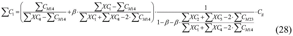
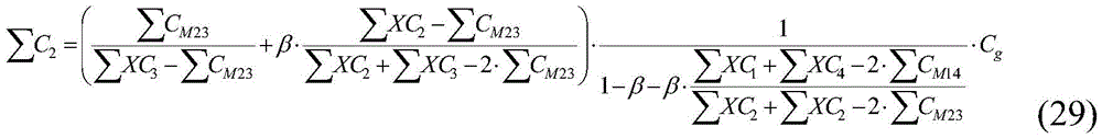

在等式(28)至(31)中,可仅有Cg和β是未知量,尽管β可近似为根据电容场模拟结果的适当常数。剩余的项可以是从四个自电容测量和两个互电容测量(例如,∑XC4、∑CM14等)得到的测量量。可将等式(28)至(31)中的相应一个等式代入到缩放因子等式(16)至(19),以获取K1、K2、K3和K4的表达式。例如,可将等式(31)代入等式(16),以获取K1的以下表达式:In equations (28) to (31), only C g and β may be unknowns, although β may be approximated as a suitable constant from capacitive field simulation results. The remaining terms may be measurements derived from four self-capacitance measurements and two mutual-capacitance measurements (eg, ΣXC4 , ΣC M14 , etc.). A corresponding one of equations (28) to (31) can be substituted into scaling factor equations ( 16 ) to ( 19 ) to obtain expressions for K1, K2, K3 and K4 . For example, equation (31) can be substituted into equation ( 16 ) to obtain the following expression for K1:

其中:in:

在等式(32)中,可仅有β是未知量,由于等式(16)和(31)中的Cg可从分子和分母中消掉。β可近似为根据电容场模拟结果的适当常数,并且剩余项可以是已知的测量量(例如,∑XC4、∑CM14等)。因此,可基于在本公开的触摸屏上获取的四个自电容和两个互电容测量来确定K1。然后可利用K1对从触摸屏上位置1处的触摸节点电极获取的自电容测量进行缩放,以有效地消除可能由部分自举式触摸屏导致的衰减。可类似地利用由以下等式表示的适当缩放因子来从对触摸屏上位置2、位置3和位置4处的触摸节点电极获取的自电容测量进行缩放,以有效地消除它们各自的衰减:In equation (32), only β may be unknown, since C g in equations (16) and (31) can be eliminated from the numerator and denominator. β can be approximated by an appropriate constant from the capacitive field simulation results, and the remaining terms can be known measurements (eg, ΣXC4 , ΣC M14 , etc.). Therefore, K 1 may be determined based on four self-capacitance and two mutual capacitance measurements taken on the touch screen of the present disclosure. Self-capacitance measurements taken from the touch node electrode at position 1 on the touchscreen can then be scaled with K1 to effectively remove the attenuation that may be caused by a partially bootstrapped touchscreen. Self-capacitance measurements taken for touch node electrodes at
作为利用各个缩放因子对相应位置处的触摸节点电极进行缩放的替代做法,在一些示例中,可利用一个平均缩放因子来缩放在触摸屏上的所有触摸节点电极处获取的所有自电容测量。该平均缩放因子可以提供足够的精度,使得可不需要个体化的缩放因子。部分自举式触摸屏的平均缩放因子可被表达为:As an alternative to scaling touch node electrodes at respective locations with individual scaling factors, in some examples, one average scaling factor may be used to scale all self-capacitance measurements taken at all touch node electrodes on the touch screen. This average scaling factor may provide sufficient accuracy such that individual scaling factors may not be required. The average scaling factor for a partially bootstrapped touchscreen can be expressed as:
如上所述,可通过利用缩放因子缩放触摸信号来有效地消除可在本公开的触摸屏上检测到的触摸信号的衰减,所述缩放因子可使用四个自电容测量和两个互电容测量来确定。可使用上文在水排斥的上下文中描述的完全自举扫描、部分自举扫描和/或互电容扫描的任何组合来捕获这些测量。As described above, the attenuation of touch signals detectable on touchscreens of the present disclosure can be effectively eliminated by scaling the touch signals using a scaling factor that can be determined using four self-capacitance measurements and two mutual-capacitance measurements . These measurements can be captured using any combination of full bootstrap scans, partial bootstrap scans, and/or mutual capacitance scans described above in the context of water repulsion.
上述未接地的用户补偿方案可应用于部分自举式触摸屏。在一些示例中,对于完全自举式触摸屏可能需要未接地的用户补偿(例如,在图14D 中的过程1451中)。完全自举式触摸屏的未接地的用户补偿可采用类似于部分自举式触摸屏的未接地的用户补偿的方式执行,如下所述。The above ungrounded user compensation scheme can be applied to some bootstrap touchscreens. In some examples, ungrounded user compensation may be required for a fully bootstrapped touchscreen (eg, in
具体地,重新参考图5A,完全自举式触摸屏的衰减因子可由等式(2)表达,并且在任何一个触摸节点电极处感测到的有效自电容可由等式(4)表达,它们均在下面再现:Specifically, referring back to FIG. 5A, the attenuation factor of a fully bootstrapped touch screen can be expressed by Equation (2), and the effective self-capacitance sensed at any one touch node electrode can be expressed by Equation (4), both of which are in The following reproduces:
α=Cg/C总 (2)α=Cg/ Ctotal ( 2)
C有效,X=α*CX (4)C is valid, X = α*C X (4)
其中C总=Cg+C1+C2+C3+C4(等式(3)),并且CX可以是C1 503、C2 where Ctotal =Cg+ C1 +C2 + C3 + C4 (equation ( 3 )), and Cx can be C1503 , C2
505、C3 507或C4 509。因此,为了基本上消除上述衰减,可利用缩放因子 1/α或C总/Cg来缩放触摸节点的自电容值。505,
如前所述,可使用互电容测量来确定上述适当的完全自举缩放因子。具体地,图15B至图15C的互电容扫描可用于获取经过手指的互电容测量,该测量可被表达为:As previously mentioned, mutual capacitance measurements can be used to determine the appropriate full bootstrap scaling factors described above. Specifically, the mutual capacitance scans of FIGS. 15B-15C can be used to obtain a mutual capacitance measurement across the finger, which can be expressed as:
∑CM=(∑CFD*∑CFS)/C总 (38)∑C M =(∑C FD *∑C FS )/ Ctotal (38)
其中∑CFD可以是所有驱动触摸节点电极到手指电容之和(例如,图15C中的配置1510中的∑C1),并且∑CFS可以是所有感测触摸节点电极到手指电容之和(例如,图15C中的配置1512中的∑C4)。等式(38)可与在完全自举式触摸屏扫描期间获取的有效自电容测量结合(例如,等式(4)),以提供完全自举缩放因子的等式:where ΣC FD may be the sum of all drive touch node electrodes to finger capacitances (eg, ΣC 1 in
KFB=C总/Cg=∑CM/∑C有效,FS+∑CM/∑C有效,FD+1 (39)K FB = C total /C g = ∑C M /∑C valid, FS +∑C M /∑C valid, FD +1 (39)
由于上述互电容测量可能包含对角触摸节点电极之间的直接互电容效应(如前所述),因此上述完全自举缩放因子可能包含一些非理想因素,其可被表达为:Since the above mutual capacitance measurements may contain direct mutual capacitance effects between the diagonal touch node electrodes (as previously discussed), the above fully bootstrapped scaling factors may contain some non-ideal factors, which can be expressed as:
KFB,理想=KFB,非理想/(1-β) (40)K FB, ideal = K FB, non-ideal /(1-β) (40)
其中β可以表达为:where β can be expressed as:
β=∑CNM/((∑CFS*∑CFD)/(∑CFS+∑CFD)) (41)β=∑C NM /((∑C FS *∑C FD )/(∑C FS +∑C FD )) (41)
其中∑CNM可以是触摸屏上的触摸节点电极之间(例如,图15C中的配置 1510中的触摸节点电极1和4之间)的总直接互电容(“近似互电容”)。可以使用场软件模拟来表明β对准确触摸位置的依赖性可很小,因此不需要在上文中加以考虑,或者可使用场软件模拟来确定。where ΣC NM may be the total direct mutual capacitance ("approximate mutual capacitance") between touch node electrodes on the touch screen (eg, between
基于等式(38),图15C所示的两个互电容配置的经过手指互电容可被表达为:Based on Equation (38), the through-finger mutual capacitance of the two mutual capacitance configurations shown in Figure 15C can be expressed as:
CM14=(C1*C4)/C总 (42)C M14 = (C 1 *C 4 )/C total (42)
CM23=(C2*C3)/C总 (43)C M23 = (C 2 *C 3 )/C total (43)
此外,基于等式(2)和(4),在图5A中的每个触摸节点处测量的有效自电容(XCy)可被表达为:Furthermore, based on equations (2) and (4), the effective self-capacitance (XC y ) measured at each touch node in FIG. 5A can be expressed as:
XC1=Cg/C总*C1 (44)XC 1 =C g /C total *C 1 (44)
XC2=Cg/C总*C2 (45)XC 2 =C g /C total *C 2 (45)
XC3=Cg/C总*C3 (46)XC 3 =C g /C total *C 3 (46)
XC4=Cg/C总*C4 (47)XC 4 =C g /C total *C 4 (47)
将上述的完全自举有效测量和互电容测量结合起来(例如,图5A的扫描和图15C的扫描得到等式(42)至(47)),可确定理想的完全自举缩放因子可被表达为:Combining the above-described fully bootstrapped effective measurements and mutual capacitance measurements (eg, the scan of Figure 5A and the scan of Figure 15C yields equations (42) through (47)), it is determined that the ideal fully bootstrapped scaling factor can be expressed as for:
KFB,理想=∑CM14/∑XC4+∑CM14/∑XC1+∑CM23/∑XC3+K FB, ideal = ∑C M14 /∑XC 4 +∑C M14 /∑XC 1 +∑C M23 /∑XC 3 +
∑CM23/∑XC2+1 (48)∑C M23 /∑XC 2 +1 (48)
其中∑XCy可表示在完全自举扫描期间在触摸屏上的触摸节点电极和手指之间的总测量自电容,并且∑CMyz可表示触摸屏上的总测量经过手指互电容。where ΣXCy may represent the total measured self-capacitance between the touch node electrodes and the finger on the touch screen during a full bootstrap scan, and ΣC Myz may represent the total measured through-finger mutual capacitance on the touch screen.
非理想因素可以通过β来解决,如上面在等式(40)中所讨论的。具体地,对于图15C所示的配置,β的等式(41)可被表达如下:Non-idealities can be accounted for by β, as discussed above in equation (40). Specifically, for the configuration shown in Figure 15C, equation (41) for β can be expressed as follows:
β=∑CNM14/((∑C4*∑C1)/(∑C4+∑C1))+β= ∑C NM14 /((∑C 4 *∑C 1 )/(∑C 4 +∑C 1 ))+
∑CNM23/((∑C3*∑C2)/(∑C3+∑C2)) (49)∑C NM23 /((∑C 3 *∑C 2 )/(∑C 3 +∑C 2 )) (49)
因此,使用上述关系,可对完全自举的触摸屏执行未接地的用户补偿。Therefore, using the above relationship, ungrounded user compensation can be performed for a fully bootstrapped touchscreen.
因此,本公开的示例提供了用于在触摸屏上检测水和水排斥以及在具有或不具有未接地的用户补偿的情况下这样做的一种或多种配置。Accordingly, examples of the present disclosure provide one or more configurations for detecting water and water repulsion on a touch screen and doing so with or without ungrounded user compensation.
因此,根据上述内容,本公开的一些示例涉及一种触摸传感器面板,该触摸传感器面板包括:多个触摸节点电极;以及触摸控制器,该触摸控制器被配置为:以完全自举的配置来驱动和感测多个触摸节点电极,以获取完全自举的触摸图像;以不同于该完全自举的配置的第二配置来驱动和感测多个触摸节点电极,以获取第二触摸图像,该第二触摸图像包括水对该触摸传感器面板的影响;并且基于完全自举的触摸图像和第二触摸图像来确定最终触摸图像,该最终触摸图像补偿水对该触摸传感器面板的影响。除上文公开的示例中的一个或多个示例之外或作为另外一种选择,在一些示例中,该第二配置包括互电容配置。除上文公开的示例中的一个或多个示例之外或作为另外一种选择,在一些示例中,该第二配置包括部分自举的配置。除上文公开的示例中的一个或多个示例之外或作为另外一种选择,在一些示例中,该最终触摸图像包括触摸传感器面板的第一部分的触摸图像,该触摸传感器面板包括触摸传感器面板的第一部分和触摸传感器面板的第二部分。除上文公开的示例中的一个或多个示例之外或作为另外一种选择,在一些示例中,该触摸传感器面板的第一部分包括多个触摸节点电极。除上文公开的示例中的一个或多个示例之外或作为另外一种选择,在一些示例中,该触摸传感器面板的第一部分包括多个触摸节点电极的第一部分,该多个触摸节点电极包括多个触摸节点电极的第一部分和多个触摸节点电极的第二部分。除上文公开的示例中的一个或多个示例之外或作为另外一种选择,在一些示例中,该触摸控制器被配置为在触摸帧期间以完全自举的配置来驱动和感测多个触摸节点电极并且以第二配置来驱动和感测多个触摸节点电极。除上文公开的示例中的一个或多个示例之外或作为另外一种选择,在一些示例中,该触摸控制器被配置为以分辨率降低的完全自举的配置驱动和感测多个触摸节点电极。除上文公开的示例中的一个或多个示例之外或作为另外一种选择,在一些示例中,该触摸控制器被配置为以分辨率降低的第二配置来驱动和感测多个触摸节点电极。除上文公开的示例中的一个或多个示例之外或作为另外一种选择,在一些示例中,该触摸控制器被配置为检测触摸传感器面板上的触摸活动并基于该触摸活动来确定第二配置。Accordingly, in light of the foregoing, some examples of the present disclosure relate to a touch sensor panel comprising: a plurality of touch node electrodes; and a touch controller configured to: in a fully bootstrapped configuration driving and sensing the plurality of touch node electrodes to obtain a fully bootstrapped touch image; driving and sensing the plurality of touch node electrodes in a second configuration different from the fully bootstrapped configuration to obtain a second touch image, The second touch image includes the effect of water on the touch sensor panel; and a final touch image is determined based on the fully bootstrapped touch image and the second touch image, the final touch image compensating for the effect of water on the touch sensor panel. In addition to or alternatively to one or more of the examples disclosed above, in some examples, the second configuration includes a mutual capacitance configuration. In addition to or alternatively to one or more of the examples disclosed above, in some examples, the second configuration includes a partially bootstrapped configuration. In addition to or alternatively to one or more of the examples disclosed above, in some examples, the final touch image includes a touch image of a first portion of a touch sensor panel that includes a touch sensor panel the first part and the second part of the touch sensor panel. In addition to or alternatively to one or more of the examples disclosed above, in some examples, the first portion of the touch sensor panel includes a plurality of touch node electrodes. In addition to or alternatively to one or more of the examples disclosed above, in some examples, the first portion of the touch sensor panel includes a first portion of a plurality of touch node electrodes that A first portion of the plurality of touch node electrodes and a second portion of the plurality of touch node electrodes are included. In addition to or alternatively to one or more of the examples disclosed above, in some examples, the touch controller is configured to drive and sense multiple touch node electrodes and drive and sense the plurality of touch node electrodes in the second configuration. In addition to or alternatively to one or more of the examples disclosed above, in some examples, the touch controller is configured to drive and sense multiple Touch the node electrode. In addition to or alternatively to one or more of the examples disclosed above, in some examples, the touch controller is configured to drive and sense multiple touches in a second, reduced resolution configuration node electrode. In addition to or alternatively to one or more of the examples disclosed above, in some examples, the touch controller is configured to detect touch activity on the touch sensor panel and determine a first touch based on the touch activity Second configuration.
本公开的一些示例涉及一种方法,该方法包括:以完全自举的配置来驱动和感测触摸传感器面板上的多个触摸节点电极,以获取完全自举的触摸图像;以不同于该完全自举的配置的第二配置来驱动和感测多个触摸节点电极,以获取第二触摸图像,该第二触摸图像包括水对该触摸传感器面板的影响;并且基于完全自举的触摸图像和第二触摸图像来确定最终触摸图像,该最终触摸图像补偿水对该触摸传感器面板的影响。除上文公开的示例中的一个或多个示例之外或作为另外一种选择,在一些示例中,该第二配置包括互电容配置。除上文公开的示例中的一个或多个示例之外或作为另外一种选择,在一些示例中,该第二配置包括部分自举的配置。除上文公开的示例中的一个或多个示例之外或作为另外一种选择,在一些示例中,该最终触摸图像包括触摸传感器面板的第一部分的触摸图像,该触摸传感器面板包括触摸传感器面板的第一部分和触摸传感器面板的第二部分。除上文公开的示例中的一个或多个示例之外或作为另外一种选择,在一些示例中,该触摸传感器面板的第一部分包括多个触摸节点电极。除上文公开的示例中的一个或多个示例之外或作为另外一种选择,在一些示例中,触摸传感器面板的第一部分包括多个触摸节点电极的第一部分,该多个触摸节点电极包括多个触摸节点电极的第一部分和多个触摸节点电极的第二部分。除上文公开的示例中的一个或多个示例之外或作为另外一种选择,在一些示例中,以完全自举的配置来驱动和感测多个触摸节点电极和以第二配置来驱动和感测多个触摸节点电极是在触摸帧期间进行的。除上文公开的示例中的一个或多个示例之外或作为另外一种选择,在一些示例中,以完全自举的配置来驱动和感测多个触摸节点电极包括以分辨率降低的完全自举的配置驱动和感测多个触摸节点电极。除上文公开的示例中的一个或多个示例之外或作为另外一种选择,在一些示例中,以第二配置来驱动和感测多个触摸节点电极包括以分辨率降低的第二配置来驱动和感测多个触摸节点电极。除上文公开的示例中的一个或多个示例之外或作为另外一种选择,在一些示例中,该方法进一步包括:检测触摸传感器面板上的触摸活动;并且基于该触摸活动来确定第二配置。Some examples of the present disclosure relate to a method comprising: driving and sensing a plurality of touch node electrodes on a touch sensor panel in a fully bootstrapped configuration to obtain a fully bootstrapped touch image; a second configuration of the bootstrapped configuration to drive and sense the plurality of touch node electrodes to obtain a second touch image including the effect of water on the touch sensor panel; and based on the fully bootstrapped touch image and The second touch image determines a final touch image that compensates for the effect of water on the touch sensor panel. In addition to or alternatively to one or more of the examples disclosed above, in some examples, the second configuration includes a mutual capacitance configuration. In addition to or alternatively to one or more of the examples disclosed above, in some examples, the second configuration includes a partially bootstrapped configuration. In addition to or alternatively to one or more of the examples disclosed above, in some examples, the final touch image includes a touch image of a first portion of a touch sensor panel that includes a touch sensor panel the first part and the second part of the touch sensor panel. In addition to or alternatively to one or more of the examples disclosed above, in some examples, the first portion of the touch sensor panel includes a plurality of touch node electrodes. In addition to or alternatively to one or more of the examples disclosed above, in some examples, the first portion of the touch sensor panel includes a first portion of a plurality of touch node electrodes that include A first portion of the plurality of touch node electrodes and a second portion of the plurality of touch node electrodes. In addition to or alternatively to one or more of the examples disclosed above, in some examples, the plurality of touch node electrodes are driven and sensed in a fully bootstrapped configuration and driven in a second configuration and sensing multiple touch node electrodes during a touch frame. In addition to or alternatively to one or more of the examples disclosed above, in some examples, driving and sensing the plurality of touch node electrodes in a fully bootstrapped configuration includes fully The bootstrapped configuration drives and senses multiple touch node electrodes. In addition to or alternatively to one or more of the examples disclosed above, in some examples, driving and sensing the plurality of touch node electrodes in the second configuration includes the second configuration with reduced resolution to drive and sense multiple touch node electrodes. In addition to or alternatively to one or more of the examples disclosed above, in some examples, the method further includes: detecting touch activity on the touch sensor panel; and determining a second based on the touch activity configuration.
虽然参照附图对本公开的示例进行了全面的描述,但应注意,各种变化和修改对于本领域内的技术人员而言将变得显而易见。应当理解,此类变化和修改被认为被包括在由所附权利要求所限定的本公开的示例的范围内。Although the examples of the present disclosure have been fully described with reference to the accompanying drawings, it is to be noted that various changes and modifications will become apparent to those skilled in the art. It should be understood that such changes and modifications are considered to be included within the scope of the examples of the present disclosure as defined by the appended claims.
Claims (19)
Priority Applications (1)
| Application Number | Priority Date | Filing Date | Title |
|---|---|---|---|
| CN202011300207.2A CN112379792B (en) | 2014-10-27 | 2015-10-27 | Pixelated self-capacitive water repellent |
Applications Claiming Priority (3)
| Application Number | Priority Date | Filing Date | Title |
|---|---|---|---|
| US201462069231P | 2014-10-27 | 2014-10-27 | |
| US62/069,231 | 2014-10-27 | ||
| PCT/US2015/057644 WO2016069642A1 (en) | 2014-10-27 | 2015-10-27 | Pixelated self-capacitance water rejection |
Related Child Applications (1)
| Application Number | Title | Priority Date | Filing Date |
|---|---|---|---|
| CN202011300207.2A Division CN112379792B (en) | 2014-10-27 | 2015-10-27 | Pixelated self-capacitive water repellent |
Publications (2)
| Publication Number | Publication Date |
|---|---|
| CN107077262A CN107077262A (en) | 2017-08-18 |
| CN107077262B true CN107077262B (en) | 2020-11-10 |
Family
ID=55858268
Family Applications (2)
| Application Number | Title | Priority Date | Filing Date |
|---|---|---|---|
| CN201580058366.7A Active CN107077262B (en) | 2014-10-27 | 2015-10-27 | Pixelization from capacitive water repellence |
| CN202011300207.2A Active CN112379792B (en) | 2014-10-27 | 2015-10-27 | Pixelated self-capacitive water repellent |
Family Applications After (1)
| Application Number | Title | Priority Date | Filing Date |
|---|---|---|---|
| CN202011300207.2A Active CN112379792B (en) | 2014-10-27 | 2015-10-27 | Pixelated self-capacitive water repellent |
Country Status (4)
| Country | Link |
|---|---|
| US (2) | US10712867B2 (en) |
| EP (1) | EP3213173B1 (en) |
| CN (2) | CN107077262B (en) |
| WO (1) | WO2016069642A1 (en) |
Families Citing this family (118)
| Publication number | Priority date | Publication date | Assignee | Title |
|---|---|---|---|---|
| US20090174676A1 (en) | 2008-01-04 | 2009-07-09 | Apple Inc. | Motion component dominance factors for motion locking of touch sensor data |
| US8922521B2 (en) | 2009-02-02 | 2014-12-30 | Apple Inc. | Switching circuitry for touch sensitive display |
| US8593410B2 (en) | 2009-04-10 | 2013-11-26 | Apple Inc. | Touch sensor panel design |
| US8957874B2 (en) | 2009-06-29 | 2015-02-17 | Apple Inc. | Touch sensor panel design |
| US9329723B2 (en) | 2012-04-16 | 2016-05-03 | Apple Inc. | Reconstruction of original touch image from differential touch image |
| US10936120B2 (en) | 2014-05-22 | 2021-03-02 | Apple Inc. | Panel bootstraping architectures for in-cell self-capacitance |
| US10289251B2 (en) | 2014-06-27 | 2019-05-14 | Apple Inc. | Reducing floating ground effects in pixelated self-capacitance touch screens |
| US9880655B2 (en) | 2014-09-02 | 2018-01-30 | Apple Inc. | Method of disambiguating water from a finger touch on a touch sensor panel |
| WO2016048269A1 (en) | 2014-09-22 | 2016-03-31 | Onamp Research Llc | Ungrounded user signal compensation for pixelated self-capacitance touch sensor panel |
| CN107077262B (en) | 2014-10-27 | 2020-11-10 | 苹果公司 | Pixelization from capacitive water repellence |
| US10795488B2 (en) | 2015-02-02 | 2020-10-06 | Apple Inc. | Flexible self-capacitance and mutual capacitance touch sensing system architecture |
| US10488992B2 (en) | 2015-03-10 | 2019-11-26 | Apple Inc. | Multi-chip touch architecture for scalability |
| US11907484B2 (en) | 2015-06-22 | 2024-02-20 | Sigmasense, Llc. | Function and orientation identification for input/output (I/O) operative touch sensor device (TSD) |
| US10664098B2 (en) | 2015-06-22 | 2020-05-26 | Sigmasense, Llc. | Channel driver circuit |
| US11397492B2 (en) | 2015-06-22 | 2022-07-26 | Sigmasense, Llc. | Enhanced mutual capacitance touch screen display with shape detection and methods for use therewith |
| KR101948453B1 (en) | 2015-07-06 | 2019-02-14 | 시그마센스, 엘엘씨. | Pen system with internal pressure tilt rotation |
| US10365773B2 (en) | 2015-09-30 | 2019-07-30 | Apple Inc. | Flexible scan plan using coarse mutual capacitance and fully-guarded measurements |
| US12121773B2 (en) | 2016-08-18 | 2024-10-22 | Sigmasense, Llc. | Personal athlete monitoring system |
| US12181352B2 (en) | 2021-06-03 | 2024-12-31 | Sigmasense, Llc. | Insole XYZ force detection system |
| US12194344B2 (en) | 2016-08-18 | 2025-01-14 | Sigmasense, Llc. | Plurality of layers of pressure sensors within a foot force detection system |
| US11246507B2 (en) | 2016-08-18 | 2022-02-15 | Sigmasense, Llc. | Wireless in-shoe physical activity monitoring apparatus |
| US12207703B2 (en) | 2016-08-18 | 2025-01-28 | Sigmasense, Llc. | Shoe to shoe communication within a foot force detection system |
| US12446798B2 (en) | 2016-08-18 | 2025-10-21 | Sigmasense, Llc. | Personal monitoring system for monitoring body conditions using e-field communications |
| US12226674B2 (en) | 2016-08-18 | 2025-02-18 | Sigmasense, Llc. | Power harvesting in a foot force detection system |
| US12225979B2 (en) | 2016-08-18 | 2025-02-18 | Sigmasense, Llc. | Variable sampling rate within a foot force detection system |
| AU2017208277B2 (en) | 2016-09-06 | 2018-12-20 | Apple Inc. | Back of cover touch sensors |
| CN107908353B (en) * | 2016-09-30 | 2020-12-18 | 禾瑞亚科技股份有限公司 | Electronic system, touch processing device and method thereof |
| WO2018082002A1 (en) * | 2016-11-04 | 2018-05-11 | 深圳市汇顶科技股份有限公司 | Terminal water entry protection method and electronic device |
| US10642418B2 (en) | 2017-04-20 | 2020-05-05 | Apple Inc. | Finger tracking in wet environment |
| JP2018190095A (en) * | 2017-04-28 | 2018-11-29 | 株式会社ジャパンディスプレイ | Detection device, display device and detection method |
| US10901557B2 (en) * | 2017-05-19 | 2021-01-26 | Elo Touch Solutions, Inc. | PCAP with enhanced immunity to water contaminants |
| US10558306B2 (en) | 2017-06-12 | 2020-02-11 | Himax Technologies Limited | In-cell touch apparatus and a water mode detection method thereof |
| TWI624778B (en) * | 2017-07-05 | 2018-05-21 | 奇景光電股份有限公司 | In-cell touch apparatus and water mode detection method thereof |
| US10838530B2 (en) | 2017-09-15 | 2020-11-17 | Sigmasense, Llc. | Touchscreen display with concurrent touch and display operations |
| US10545614B2 (en) | 2018-01-22 | 2020-01-28 | Cypress Semiconductor Corporation | Two-electrode touch button with a multi-phase capacitance measurement process |
| CN108919997B (en) * | 2018-06-29 | 2021-06-29 | 中国联合网络通信集团有限公司 | Method and device for improving recognition accuracy of capacitive touch screen |
| US11644860B2 (en) | 2018-08-27 | 2023-05-09 | Sigmasense, Llc. | Configuring a programmable drive sense unit |
| US11550426B2 (en) | 2018-08-27 | 2023-01-10 | Sigmasense, Llc. | Sensor monitoring system |
| US10895867B2 (en) | 2018-08-27 | 2021-01-19 | Sigmasense, Llc. | Analog world interfacing for automated systems |
| US11914812B2 (en) | 2018-08-27 | 2024-02-27 | Sigmasense, Llc. | Current reference operative drive-sense circuit (DSC) |
| US11003205B2 (en) | 2019-02-04 | 2021-05-11 | Sigmasense, Llc. | Receive analog to digital circuit of a low voltage drive circuit data communication system |
| US11429226B2 (en) | 2018-08-27 | 2022-08-30 | Sigmasense, Llc. | Analog-digital drive sense circuit |
| US10554215B1 (en) | 2019-03-26 | 2020-02-04 | Sigmasense, Llc. | Analog to digital conversion circuit with very narrow bandpass digital filtering |
| US11099032B2 (en) | 2018-08-27 | 2021-08-24 | Sigmasense, Llc. | Drive sense circuit with drive-sense line |
| US12007421B2 (en) | 2018-08-27 | 2024-06-11 | Sigmasense, Llc. | Load sensing circuit employing sink and sense configuration |
| US11635396B2 (en) | 2018-08-27 | 2023-04-25 | Sigmasense, Llc. | Sensing device with drive sense circuit and particle sensor and methods for use therewith |
| US11822358B2 (en) | 2018-08-27 | 2023-11-21 | Sigmasense, Llc. | Drive-sense circuit to determine effects of different electrical characteristics on load |
| US11899867B2 (en) | 2018-09-14 | 2024-02-13 | Sigmasense, Llc. | Touch screen display with touchless gestures and methods for use therewith |
| US10908718B2 (en) | 2018-09-14 | 2021-02-02 | Sigmasense, Llc. | Large touch screen display with integrated electrodes |
| US11875005B2 (en) | 2018-09-14 | 2024-01-16 | Sigmasense, Llc. | Touch screen display with touchless indications and methods for use therewith |
| US11789555B2 (en) | 2018-09-14 | 2023-10-17 | Sigmasense, Llc. | Touch sense control circuit with noise suppression |
| US10845985B2 (en) | 2018-09-14 | 2020-11-24 | Sigmasense, Llc. | Identification in touch systems |
| US11372510B2 (en) * | 2018-11-02 | 2022-06-28 | Sigmasense, Llc. | Multi-conductor touch system |
| US10852857B2 (en) | 2018-11-19 | 2020-12-01 | Sigmasense, Llc. | Frequency diverse e-pen for touch sensor and e-pen systems |
| US10935585B2 (en) | 2018-11-19 | 2021-03-02 | Sigmasense, Llc. | Drive sense circuit with transient suppression |
| US10996728B2 (en) | 2019-01-04 | 2021-05-04 | Sigmasense, Llc. | Power supply signal conditioning system based on drive-sense circuit (DSC) processing |
| US10831690B2 (en) | 2019-01-14 | 2020-11-10 | Sigmasense, Llc. | Channel allocation among low voltage drive circuits |
| US10915483B2 (en) | 2019-01-14 | 2021-02-09 | Sigmasense, Llc. | Low voltage drive circuit with variable oscillating characteristics and methods for use therewith |
| CN111610873B (en) * | 2019-02-26 | 2023-10-27 | 敦泰电子有限公司 | Touch control method, circuit system and touch device |
| US11061082B2 (en) | 2019-03-18 | 2021-07-13 | Sigmasense, Llc. | Single line hall effect sensor drive and sense |
| US10671034B1 (en) | 2019-03-18 | 2020-06-02 | Sigmasense, Llc. | Motor drive input adaptation with in-line drive-sense circuit |
| US12046214B2 (en) | 2019-03-22 | 2024-07-23 | Sigmasense, Llc. | Display controller with row enable based on drive settle detection |
| US11016617B2 (en) * | 2019-04-12 | 2021-05-25 | Egalax_Empia Technology Inc. | Touch sensitive processing method and apparatus and touch sensitive system |
| US11029782B2 (en) | 2019-05-03 | 2021-06-08 | Sigmasense, Llc. | Light emitting diode (LED) touch display circuit |
| US10756578B1 (en) | 2019-05-31 | 2020-08-25 | Sigmasense, Llc. | Wireless power transfer with in-line sensing and control |
| US11056930B2 (en) | 2019-05-31 | 2021-07-06 | Sigmasense, Llc. | Wireless power transfer and communications |
| US11131714B2 (en) | 2019-05-31 | 2021-09-28 | Sigmasense, Llc. | Battery monitoring and characterization during charging |
| US11221709B2 (en) | 2019-06-10 | 2022-01-11 | Sigmasense, Llc. | Electronic writing apparatus with ring-back and other functionalities |
| US11216133B2 (en) | 2019-06-10 | 2022-01-04 | Sigmasense, Llc. | Device for use with a touch screen |
| US11126297B2 (en) | 2019-06-10 | 2021-09-21 | Sigmasense, Llc. | Electronic pen with ring-back and other functionalities |
| US11555687B2 (en) | 2019-08-08 | 2023-01-17 | Sigmasense, Llc. | Capacitive imaging glove |
| US10976837B2 (en) | 2019-08-20 | 2021-04-13 | Sigmasense, Llc. | User input passive device for use with an interactive display device |
| US11157109B1 (en) | 2019-09-06 | 2021-10-26 | Apple Inc. | Touch sensing with water rejection |
| US11017845B2 (en) | 2019-09-11 | 2021-05-25 | Sigmasense, Llc. | RAM cell processing circuit for concurrency of refresh and read |
| US10908641B1 (en) | 2019-10-09 | 2021-02-02 | Sigmasense, Llc. | Display generated data transmission from user device to touchscreen via user |
| US11221980B2 (en) | 2019-10-31 | 2022-01-11 | Sigmasense, Llc. | Low voltage drive circuit operable to convey data via a bus |
| US11133811B2 (en) | 2019-11-08 | 2021-09-28 | Sigmasense, Llc. | High resolution analog to digital converter (ADC) with improved bandwidth |
| US11190205B2 (en) | 2019-11-08 | 2021-11-30 | Sigmasense, Llc. | Single-ended direct interface dual DAC feedback photo-diode sensor |
| US10862492B1 (en) | 2019-11-08 | 2020-12-08 | Sigmasense, Llc. | Current operative analog to digital converter (ADC) |
| US11709189B2 (en) | 2019-11-08 | 2023-07-25 | Sigmasense, Llc. | Two-element high accuracy impedance sensing circuit with increased signal to noise ratio (SNR) |
| US12352713B2 (en) | 2019-12-30 | 2025-07-08 | Sigmasense, Llc. | Organic and/or inorganic material test system using differential drive-sense circuits |
| US11935397B2 (en) | 2019-12-30 | 2024-03-19 | Sigmasense, Llc. | Organic and inorganic test system |
| US11216109B2 (en) | 2020-01-07 | 2022-01-04 | Sigmasense, Llc. | Drive-sense control for extended sensor panels |
| US11221704B2 (en) | 2020-02-05 | 2022-01-11 | Sigmasense, Llc. | Screen-to-screen communication via touch sense elements |
| US11079888B1 (en) | 2020-02-18 | 2021-08-03 | Sigmasense, Llc. | Sensitivity region of interest processing (ROIP) for input/output (I/O) operative touch sensor device (TSD) |
| US11144160B1 (en) * | 2020-03-30 | 2021-10-12 | Sigmasense, Llc. | Three-dimensional data reduction method and system |
| US11182038B2 (en) | 2020-04-08 | 2021-11-23 | Sigmasense, Llc. | Encoded data pattern touchscreen sensing system |
| US11340995B2 (en) | 2020-05-21 | 2022-05-24 | Sigmasense, Llc. | Integrated circuit with programmable input/output module |
| TWI737318B (en) * | 2020-05-27 | 2021-08-21 | 禾瑞亞科技股份有限公司 | Touch sensitive processing method, apparatus and touch system |
| US11662867B1 (en) | 2020-05-30 | 2023-05-30 | Apple Inc. | Hover detection on a touch sensor panel |
| US11439812B2 (en) | 2020-06-03 | 2022-09-13 | Sigmasense, Llc. | Array operative to perform distributed/patterned sensing and/or stimulation across patient bodily section |
| US11504535B2 (en) | 2020-06-03 | 2022-11-22 | Sigmasense, Llc. | Pacemaker operative to deliver impulses of pace signal and sense cardiac response via single conductor of pacemaker lead |
| US11304002B2 (en) | 2020-08-12 | 2022-04-12 | Sigmasense, Llc. | Single transducer audio in/out device |
| KR102812808B1 (en) * | 2020-09-23 | 2025-05-28 | 삼성디스플레이 주식회사 | Display device |
| KR20220082315A (en) * | 2020-12-10 | 2022-06-17 | 엘지디스플레이 주식회사 | Light emitting display device with integrated touch screen |
| US11300536B1 (en) | 2020-12-18 | 2022-04-12 | Cypress Semiconductor Corporation | Non-contact liquid sensing technologies |
| US11374587B1 (en) | 2021-02-25 | 2022-06-28 | Sigmasense, Llc. | Batteryless wireless sensor system |
| US11989378B2 (en) | 2021-04-23 | 2024-05-21 | Sigmasense, Llc. | Passive pen with variable capacitor for pressure indication |
| US11575850B2 (en) | 2021-05-28 | 2023-02-07 | Sigmasense, Llc. | Imaging device with drive-sense circuit(s) and methods for use therewith |
| US11575851B2 (en) | 2021-05-28 | 2023-02-07 | Sigmasense, Llc. | Handheld communication device with drive-sense circuit based imaging array and methods for use therewith |
| US11977123B2 (en) | 2021-06-01 | 2024-05-07 | Sigmasense, Llc. | Sensing voltage using micro-watt sensor |
| US12360641B2 (en) | 2021-06-28 | 2025-07-15 | Sigmasense, Llc. | System for detecting and validating multiuser interaction with interface elements via perimeter sensors |
| US12373070B2 (en) | 2021-06-28 | 2025-07-29 | Sigmasense, Llc. | System for detecting and validating multiuser interaction with interface elements via signaling through users bodies |
| US11679678B2 (en) | 2021-06-28 | 2023-06-20 | Sigmasense, Llc. | Vehicle system for detecting and visually conveying vehicle button interaction |
| US11733818B2 (en) | 2021-07-19 | 2023-08-22 | Sigmasense, Llc. | Identifying capacitively coupled devices |
| US11556298B1 (en) | 2021-07-30 | 2023-01-17 | Sigmasense, Llc | Generation and communication of user notation data via an interactive display device |
| US11592874B1 (en) | 2021-08-04 | 2023-02-28 | Sigmasense, Llc. | Touch sensing in a flexible/foldable touch screen display |
| US11797139B2 (en) | 2021-09-21 | 2023-10-24 | Sigmasense, Llc. | Fingerprint scanning device incorporating drive-sense circuitry |
| US11435864B1 (en) | 2021-09-28 | 2022-09-06 | Sigmasense, Llc. | Differential touch screen display |
| US11709563B2 (en) | 2021-10-26 | 2023-07-25 | Sigmasense, Llc. | Touch-based device with interlaced electrode grids |
| US12271550B2 (en) | 2022-04-28 | 2025-04-08 | Sigmasense, Llc. | Multi-frequency character transmission and detection |
| US12360630B2 (en) | 2022-06-03 | 2025-07-15 | Sigmasense, Llc. | Touch sensor device with differentiated priority sensing region |
| US11740752B1 (en) | 2022-07-13 | 2023-08-29 | Sigmasense, Llc. | Device with signal generator |
| US12175039B2 (en) | 2022-07-13 | 2024-12-24 | Sigmasense, Llc. | Touch icon offset based on touch data samples |
| US11928289B2 (en) | 2022-07-17 | 2024-03-12 | Novatek Microelectronics Corp. | Touch sensing method for non-water mode and water mode |
| US12050740B2 (en) | 2022-11-29 | 2024-07-30 | Sigmasense, Llc. | Passive device with compressible pressure assembly for Z-direction capacitance detection |
| US12541267B2 (en) | 2023-04-28 | 2026-02-03 | Sigmasense, Llc. | Touch sensor noise prediction and cancellation |
| US12135852B1 (en) | 2023-04-28 | 2024-11-05 | Sigmasense, Llc. | Spatial filtering a touch signal of a touch screen display |
Citations (2)
| Publication number | Priority date | Publication date | Assignee | Title |
|---|---|---|---|---|
| CN102411460A (en) * | 2010-09-17 | 2012-04-11 | 索尼公司 | Display apparatus, driving method and driving circuit therefor, and electronic apparatus |
| CN103221910A (en) * | 2010-08-27 | 2013-07-24 | Uico公司 | Capacitive touch screen having dynamic capacitance control and improved touch-ensing |
Family Cites Families (449)
| Publication number | Priority date | Publication date | Assignee | Title |
|---|---|---|---|---|
| US3040142A (en) | 1959-10-22 | 1962-06-19 | Arrow Hart & Hegeman Electric | Lighted push button starting switch |
| US4090092A (en) | 1976-07-16 | 1978-05-16 | General Electric Company | Shielding arrangement for a capacitive touch switch device |
| US4087625A (en) | 1976-12-29 | 1978-05-02 | International Business Machines Corporation | Capacitive two dimensional tablet with single conductive layer |
| US4304976A (en) | 1978-03-16 | 1981-12-08 | Texas Instruments Incorporated | Capacitive touch switch panel |
| US4475235A (en) | 1982-01-04 | 1984-10-02 | Rolm Corporation | Signature verification sensor |
| IT1194351B (en) | 1983-07-28 | 1988-09-22 | Snam Progetti | PROCEDURE FOR THE RECOVERY OF BUTENE-1 DEGREE POLYMERIZATION |
| US4550221A (en) | 1983-10-07 | 1985-10-29 | Scott Mabusth | Touch sensitive control device |
| US4659874A (en) | 1985-09-23 | 1987-04-21 | Sanders Associates, Inc. | X-Y position sensor |
| US5459463A (en) | 1990-05-25 | 1995-10-17 | Sextant Avionique | Device for locating an object situated close to a detection area and a transparent keyboard using said device |
| GB2245708A (en) | 1990-06-29 | 1992-01-08 | Philips Electronic Associated | Touch sensor array systems |
| US5483261A (en) | 1992-02-14 | 1996-01-09 | Itu Research, Inc. | Graphical input controller and method with rear screen image detection |
| US5914465A (en) | 1992-06-08 | 1999-06-22 | Synaptics, Inc. | Object position detector |
| US5488204A (en) | 1992-06-08 | 1996-01-30 | Synaptics, Incorporated | Paintbrush stylus for capacitive touch sensor pad |
| US5880411A (en) | 1992-06-08 | 1999-03-09 | Synaptics, Incorporated | Object position detector with edge motion feature and gesture recognition |
| DE69324067T2 (en) | 1992-06-08 | 1999-07-15 | Synaptics Inc | Object position detector |
| US5317919A (en) | 1992-06-16 | 1994-06-07 | Teledyne Industries, Inc. | A precision capacitor sensor |
| JP3450376B2 (en) | 1993-06-12 | 2003-09-22 | 株式会社半導体エネルギー研究所 | Method for manufacturing semiconductor device |
| JP3121715B2 (en) | 1993-10-27 | 2001-01-09 | シャープ株式会社 | Information display device |
| GB9406702D0 (en) | 1994-04-05 | 1994-05-25 | Binstead Ronald P | Multiple input proximity detector and touchpad system |
| US5591945A (en) | 1995-04-19 | 1997-01-07 | Elo Touchsystems, Inc. | Acoustic touch position sensor using higher order horizontally polarized shear wave propagation |
| US5825352A (en) | 1996-01-04 | 1998-10-20 | Logitech, Inc. | Multiple fingers contact sensing method for emulating mouse buttons and mouse operations on a touch sensor pad |
| US5835079A (en) | 1996-06-13 | 1998-11-10 | International Business Machines Corporation | Virtual pointing device for touchscreens |
| US7629969B2 (en) | 1996-08-12 | 2009-12-08 | Tyco Electronics Corporation | Acoustic condition sensor employing a plurality of mutually non-orthogonal waves |
| GB2321108A (en) | 1997-01-08 | 1998-07-15 | David Alan Woodfield | Input device for inputting positional information |
| JP3394187B2 (en) | 1997-08-08 | 2003-04-07 | シャープ株式会社 | Coordinate input device and display integrated type coordinate input device |
| US6310610B1 (en) | 1997-12-04 | 2001-10-30 | Nortel Networks Limited | Intelligent touch display |
| US6163313A (en) | 1997-12-12 | 2000-12-19 | Aroyan; James L. | Touch sensitive screen and method |
| AU2211799A (en) | 1998-01-06 | 1999-07-26 | Video Mouse Group, The | Human motion following computer mouse and game controller |
| US7663607B2 (en) | 2004-05-06 | 2010-02-16 | Apple Inc. | Multipoint touchscreen |
| KR100595924B1 (en) | 1998-01-26 | 2006-07-05 | 웨인 웨스터만 | Method and apparatus for integrating manual input |
| US8479122B2 (en) | 2004-07-30 | 2013-07-02 | Apple Inc. | Gestures for touch sensitive input devices |
| US20070177804A1 (en) | 2006-01-30 | 2007-08-02 | Apple Computer, Inc. | Multi-touch gesture dictionary |
| EP2256606B1 (en) | 1998-01-26 | 2017-08-09 | Apple Inc. | Method and apparatus for integrating manual input |
| US6329044B1 (en) | 1998-06-25 | 2001-12-11 | Asahi Glass Company Ltd. | Transparent conductive film and method of making the film |
| US6188391B1 (en) | 1998-07-09 | 2001-02-13 | Synaptics, Inc. | Two-layer capacitive touchpad and method of making same |
| US6057903A (en) | 1998-08-18 | 2000-05-02 | International Business Machines Corporation | Liquid crystal display device employing a guard plane between a layer for measuring touch position and common electrode layer |
| US7002542B2 (en) | 1998-09-19 | 2006-02-21 | Lg.Philips Lcd Co., Ltd. | Active matrix liquid crystal display |
| JP4542637B2 (en) | 1998-11-25 | 2010-09-15 | セイコーエプソン株式会社 | Portable information device and information storage medium |
| EP1153404B1 (en) | 1999-01-26 | 2011-07-20 | QRG Limited | Capacitive sensor and array |
| US6297811B1 (en) | 1999-06-02 | 2001-10-02 | Elo Touchsystems, Inc. | Projective capacitive touchscreen |
| US6730863B1 (en) | 1999-06-22 | 2004-05-04 | Cirque Corporation | Touchpad having increased noise rejection, decreased moisture sensitivity, and improved tracking |
| US7030860B1 (en) | 1999-10-08 | 2006-04-18 | Synaptics Incorporated | Flexible transparent touch sensing system for electronic devices |
| US6456952B1 (en) | 2000-03-29 | 2002-09-24 | Ncr Coporation | System and method for touch screen environmental calibration |
| GB0014074D0 (en) | 2000-06-10 | 2000-08-02 | Koninkl Philips Electronics Nv | Active matrix array devices |
| US6803906B1 (en) | 2000-07-05 | 2004-10-12 | Smart Technologies, Inc. | Passive touch system and method of detecting user input |
| US6525547B2 (en) | 2001-04-17 | 2003-02-25 | Sentronics Corporation | Capacitive two dimensional sensor |
| JP3800984B2 (en) | 2001-05-21 | 2006-07-26 | ソニー株式会社 | User input device |
| JP2003066417A (en) | 2001-08-22 | 2003-03-05 | Sharp Corp | Touch sensor integrated display |
| JP2003173237A (en) | 2001-09-28 | 2003-06-20 | Ricoh Co Ltd | Information input / output system, program and storage medium |
| US6788301B2 (en) | 2001-10-18 | 2004-09-07 | Hewlett-Packard Development Company, L.P. | Active pixel determination for line generation in regionalized rasterizer displays |
| GB2381644A (en) | 2001-10-31 | 2003-05-07 | Cambridge Display Tech Ltd | Display drivers |
| US6977646B1 (en) | 2001-11-30 | 2005-12-20 | 3M Innovative Properties Co. | Touch screen calibration system and method |
| US6690387B2 (en) | 2001-12-28 | 2004-02-10 | Koninklijke Philips Electronics N.V. | Touch-screen image scrolling system and method |
| KR20040091728A (en) | 2002-03-15 | 2004-10-28 | 코닌클리즈케 필립스 일렉트로닉스 엔.브이. | Touch sensitive display device |
| US7532202B2 (en) | 2002-05-08 | 2009-05-12 | 3M Innovative Properties Company | Baselining techniques in force-based touch panel systems |
| US11275405B2 (en) | 2005-03-04 | 2022-03-15 | Apple Inc. | Multi-functional hand-held device |
| US20040017362A1 (en) | 2002-07-23 | 2004-01-29 | Mulligan Roger C. | Thin face capacitive touch screen |
| WO2004013833A2 (en) | 2002-08-02 | 2004-02-12 | Cirque Corporation | Single-layer touchpad having touch zones |
| US7180508B2 (en) | 2002-09-17 | 2007-02-20 | Tyco Electronics Corporation | Dynamic corrections for a non-linear touchscreen |
| US20040090429A1 (en) | 2002-11-12 | 2004-05-13 | Geaghan Bernard O. | Touch sensor and method of making |
| US6970160B2 (en) | 2002-12-19 | 2005-11-29 | 3M Innovative Properties Company | Lattice touch-sensing system |
| GB2398916A (en) | 2003-02-28 | 2004-09-01 | Sharp Kk | Display and sensor apparatus |
| US7300829B2 (en) | 2003-06-02 | 2007-11-27 | Applied Materials, Inc. | Low temperature process for TFT fabrication |
| US7129935B2 (en) | 2003-06-02 | 2006-10-31 | Synaptics Incorporated | Sensor patterns for a capacitive sensing apparatus |
| WO2004112448A2 (en) | 2003-06-13 | 2004-12-23 | Semtech Corporation | Sensor for capacitive touch pad pointing device |
| GB0313808D0 (en) | 2003-06-14 | 2003-07-23 | Binstead Ronald P | Improvements in touch technology |
| KR20060083129A (en) | 2003-06-20 | 2006-07-20 | 서크 코퍼레이션 | Single-layer touch pad for use with display screens |
| US7412586B1 (en) | 2003-07-29 | 2008-08-12 | Colorado State University Research Foundation | Switch memory architectures |
| JP4496738B2 (en) | 2003-09-04 | 2010-07-07 | ソニー株式会社 | Image display device |
| US20050069718A1 (en) | 2003-09-30 | 2005-03-31 | Voss-Kehl Jessica L. | Printable insulating compositions and printable articles |
| US20050073507A1 (en) | 2003-10-06 | 2005-04-07 | Richter Paul J. | Touch input sensing device |
| US8068186B2 (en) | 2003-10-15 | 2011-11-29 | 3M Innovative Properties Company | Patterned conductor touch screen having improved optics |
| US7339579B2 (en) | 2003-12-15 | 2008-03-04 | 3M Innovative Properties Company | Wiring harness and touch sensor incorporating same |
| US7307624B2 (en) | 2003-12-30 | 2007-12-11 | 3M Innovative Properties Company | Touch sensor with linearized response |
| US9172553B2 (en) | 2005-03-16 | 2015-10-27 | Icontrol Networks, Inc. | Security system with networked touchscreen and gateway |
| JP4274027B2 (en) | 2004-04-06 | 2009-06-03 | ソニー株式会社 | Image display device and driving method of image display device |
| JP2005304855A (en) | 2004-04-22 | 2005-11-04 | Aruze Corp | Game machine |
| US7382139B2 (en) | 2004-06-03 | 2008-06-03 | Synaptics Incorporated | One layer capacitive sensing apparatus having varying width sensing elements |
| KR101133753B1 (en) | 2004-07-26 | 2012-04-09 | 삼성전자주식회사 | Liquid crystal display including sensing element |
| KR100958491B1 (en) | 2004-07-30 | 2010-05-17 | 애플 인크. | Mode-based graphical user interface for touch-sensitive input devices |
| US7719523B2 (en) | 2004-08-06 | 2010-05-18 | Touchtable, Inc. | Bounding box gesture recognition on a touch detecting interactive display |
| US7737953B2 (en) | 2004-08-19 | 2010-06-15 | Synaptics Incorporated | Capacitive sensing apparatus having varying depth sensing elements |
| KR20060062164A (en) | 2004-12-03 | 2006-06-12 | 삼성전자주식회사 | Display device with built-in light sensor |
| KR100651559B1 (en) | 2004-12-30 | 2006-11-29 | 삼성전기주식회사 | High frequency signal transmission line with improved noise characteristics |
| US20060227114A1 (en) | 2005-03-30 | 2006-10-12 | Geaghan Bernard O | Touch location determination with error correction for sensor movement |
| US20060227115A1 (en) | 2005-03-31 | 2006-10-12 | Tyco Electronic Corporation | Method and apparatus for touch sensor with interference rejection |
| US7504833B1 (en) | 2005-04-01 | 2009-03-17 | Cypress Semiconductor Corporation | Automatically balanced sensing device and method for multiple capacitive sensors |
| US7567240B2 (en) | 2005-05-31 | 2009-07-28 | 3M Innovative Properties Company | Detection of and compensation for stray capacitance in capacitive touch sensors |
| US7138686B1 (en) | 2005-05-31 | 2006-11-21 | Freescale Semiconductor, Inc. | Integrated circuit with improved signal noise isolation and method for improving signal noise isolation |
| US9019209B2 (en) | 2005-06-08 | 2015-04-28 | 3M Innovative Properties Company | Touch location determination involving multiple touch location processes |
| US7337085B2 (en) | 2005-06-10 | 2008-02-26 | Qsi Corporation | Sensor baseline compensation in a force-based touch device |
| KR101057785B1 (en) | 2005-06-30 | 2011-08-19 | 엘지디스플레이 주식회사 | Liquid crystal display device and driving method thereof |
| GB2428306B (en) | 2005-07-08 | 2007-09-26 | Harald Philipp | Two-dimensional capacitive position sensor |
| US20070012665A1 (en) | 2005-07-12 | 2007-01-18 | Hewlett-Packard Development Company Lp | Laser ablation |
| WO2007012899A1 (en) | 2005-07-25 | 2007-02-01 | Plastic Logic Limited | Flexible touch screen display |
| JP4810918B2 (en) | 2005-08-01 | 2011-11-09 | 富士ゼロックス株式会社 | Code pattern image generating apparatus and method, code pattern image reading apparatus and method, and code pattern image medium |
| KR101230303B1 (en) | 2005-08-29 | 2013-02-06 | 삼성디스플레이 주식회사 | Touch sensible display device |
| US7932898B2 (en) | 2005-09-20 | 2011-04-26 | Atmel Corporation | Touch sensitive screen |
| JP2007086990A (en) | 2005-09-21 | 2007-04-05 | Smk Corp | Touch panel |
| US7864160B2 (en) | 2005-10-05 | 2011-01-04 | 3M Innovative Properties Company | Interleaved electrodes for touch sensing |
| WO2007066488A1 (en) | 2005-12-09 | 2007-06-14 | Pioneer Corporation | Display device and touch panel operation/control method |
| US7218124B1 (en) | 2006-01-30 | 2007-05-15 | Synaptics Incorporated | Capacitive sensing apparatus designs |
| US7395717B2 (en) | 2006-02-10 | 2008-07-08 | Milliken & Company | Flexible capacitive sensor |
| JP4557228B2 (en) | 2006-03-16 | 2010-10-06 | ソニー株式会社 | Electro-optical device and electronic apparatus |
| US8144115B2 (en) | 2006-03-17 | 2012-03-27 | Konicek Jeffrey C | Flat panel display screen operable for touch position determination system and methods |
| US7538760B2 (en) | 2006-03-30 | 2009-05-26 | Apple Inc. | Force imaging input device and system |
| US8144125B2 (en) | 2006-03-30 | 2012-03-27 | Cypress Semiconductor Corporation | Apparatus and method for reducing average scan rate to detect a conductive object on a sensing device |
| US20070229470A1 (en) | 2006-03-31 | 2007-10-04 | Warren Snyder | Capacitive touch sense device having polygonal shaped sensor elements |
| US8264466B2 (en) | 2006-03-31 | 2012-09-11 | 3M Innovative Properties Company | Touch screen having reduced visibility transparent conductor pattern |
| DE202007005237U1 (en) | 2006-04-25 | 2007-07-05 | Philipp, Harald, Southampton | Touch-sensitive position sensor for use in control panel, has bus bars arranged at distance to substrate, and detection region with units that are arranged at distance by non-conductive openings such that current flows into region |
| TW200805128A (en) | 2006-05-05 | 2008-01-16 | Harald Philipp | Touch screen element |
| JP4654211B2 (en) | 2006-05-09 | 2011-03-16 | アップル インコーポレイテッド | Force / position sensing display |
| US20070262963A1 (en) | 2006-05-11 | 2007-11-15 | Cypress Semiconductor Corporation | Apparatus and method for recognizing a button operation on a sensing device |
| KR20070109360A (en) | 2006-05-11 | 2007-11-15 | 삼성전자주식회사 | Touch screen device and its noise reduction method |
| US8619054B2 (en) | 2006-05-31 | 2013-12-31 | Atmel Corporation | Two dimensional position sensor |
| CN100592201C (en) | 2006-06-02 | 2010-02-24 | 鸿富锦精密工业(深圳)有限公司 | Optical lens testing device and testing method |
| US20070283832A1 (en) | 2006-06-09 | 2007-12-13 | Apple Computer, Inc. | Imprint circuit patterning |
| KR101239019B1 (en) | 2006-06-09 | 2013-03-04 | 애플 인크. | Touch screen liquid crystal display |
| KR101246830B1 (en) | 2006-06-09 | 2013-03-28 | 삼성디스플레이 주식회사 | Display device and method of driving the same |
| US8552989B2 (en) | 2006-06-09 | 2013-10-08 | Apple Inc. | Integrated display and touch screen |
| KR101251999B1 (en) | 2006-06-13 | 2013-04-08 | 삼성디스플레이 주식회사 | Liquid crystal display device, and driving method thereof |
| US8169421B2 (en) | 2006-06-19 | 2012-05-01 | Cypress Semiconductor Corporation | Apparatus and method for detecting a touch-sensor pad gesture |
| US8068097B2 (en) | 2006-06-27 | 2011-11-29 | Cypress Semiconductor Corporation | Apparatus for detecting conductive material of a pad layer of a sensing device |
| US8022935B2 (en) | 2006-07-06 | 2011-09-20 | Apple Inc. | Capacitance sensing electrode with integrated I/O mechanism |
| US8040321B2 (en) | 2006-07-10 | 2011-10-18 | Cypress Semiconductor Corporation | Touch-sensor with shared capacitive sensors |
| US20080006454A1 (en) | 2006-07-10 | 2008-01-10 | Apple Computer, Inc. | Mutual capacitance touch sensing device |
| GB0613983D0 (en) | 2006-07-13 | 2006-08-23 | Synaptics Uk Ltd | Digitising System |
| US8599144B2 (en) | 2006-07-31 | 2013-12-03 | Cypress Semiconductor Corporation | Grounded button for capacitive sensor |
| US7825908B2 (en) | 2006-08-08 | 2010-11-02 | Carrier Corporation | Method for resetting configuration on a touchscreen interface |
| CN101122838B (en) | 2006-08-13 | 2011-06-29 | 智点科技(深圳)有限公司 | Active Touch Panel Display |
| KR100886824B1 (en) | 2006-08-18 | 2009-03-05 | 삼성전자주식회사 | Touch screen display and driving method including hybrid touch screen panel controller |
| KR101274034B1 (en) | 2006-08-25 | 2013-06-12 | 삼성디스플레이 주식회사 | Touch screen display device and method of manufacturing the same |
| US20080047764A1 (en) | 2006-08-28 | 2008-02-28 | Cypress Semiconductor Corporation | Temperature compensation method for capacitive sensors |
| US20080074398A1 (en) | 2006-09-26 | 2008-03-27 | David Gordon Wright | Single-layer capacitive sensing device |
| KR100837738B1 (en) | 2006-10-16 | 2008-06-13 | 주식회사 애트랩 | Electronic device and touch panel placement method |
| US8045783B2 (en) | 2006-11-09 | 2011-10-25 | Drvision Technologies Llc | Method for moving cell detection from temporal image sequence model estimation |
| US8547114B2 (en) | 2006-11-14 | 2013-10-01 | Cypress Semiconductor Corporation | Capacitance to code converter with sigma-delta modulator |
| TWI344127B (en) | 2006-12-05 | 2011-06-21 | Hannstar Display Corp | Liquid crystal display panel having a touch panel function |
| US8902172B2 (en) | 2006-12-07 | 2014-12-02 | Cypress Semiconductor Corporation | Preventing unintentional activation of a touch-sensor button caused by a presence of conductive liquid on the touch-sensor button |
| US8125312B2 (en) | 2006-12-08 | 2012-02-28 | Research In Motion Limited | System and method for locking and unlocking access to an electronic device |
| US20080136787A1 (en) | 2006-12-11 | 2008-06-12 | I-Hau Yeh | Touchpad having Single Layer Layout |
| US7948477B2 (en) | 2006-12-15 | 2011-05-24 | Apple Inc. | PET-based touchpad |
| US7855718B2 (en) | 2007-01-03 | 2010-12-21 | Apple Inc. | Multi-touch input discrimination |
| US8970501B2 (en) | 2007-01-03 | 2015-03-03 | Apple Inc. | Proximity and multi-touch sensor detection and demodulation |
| US8026904B2 (en) | 2007-01-03 | 2011-09-27 | Apple Inc. | Periodic sensor panel baseline adjustment |
| US8125456B2 (en) | 2007-01-03 | 2012-02-28 | Apple Inc. | Multi-touch auto scanning |
| US8269727B2 (en) | 2007-01-03 | 2012-09-18 | Apple Inc. | Irregular input identification |
| US8026903B2 (en) | 2007-01-03 | 2011-09-27 | Apple Inc. | Double-sided touch sensitive panel and flex circuit bonding |
| US8054296B2 (en) | 2007-01-03 | 2011-11-08 | Apple Inc. | Storing baseline information in EEPROM |
| US8130203B2 (en) | 2007-01-03 | 2012-03-06 | Apple Inc. | Multi-touch input discrimination |
| US7812827B2 (en) | 2007-01-03 | 2010-10-12 | Apple Inc. | Simultaneous sensing arrangement |
| US7639234B2 (en) | 2007-01-04 | 2009-12-29 | Avago Technologies Ecbu Ip (Singapore) Pte. Ltd. | Capacitive sensing and absolute position mapping in displacement type pointing devices |
| US9176318B2 (en) | 2007-05-18 | 2015-11-03 | Pixtronix, Inc. | Methods for manufacturing fluid-filled MEMS displays |
| KR20080073872A (en) | 2007-02-07 | 2008-08-12 | 엘지전자 주식회사 | Mobile communication terminal with touch screen and information input method using same |
| KR100885730B1 (en) | 2007-03-05 | 2009-02-26 | (주)멜파스 | Touch location sensing pannel having a simple layer structure |
| JP4897525B2 (en) | 2007-03-16 | 2012-03-14 | 株式会社 日立ディスプレイズ | Image display device |
| GB2447983A (en) | 2007-03-30 | 2008-10-01 | Seiko Epson Corp | Electrochromic display apparatus and method for operating said display apparatus |
| KR100858616B1 (en) | 2007-04-10 | 2008-09-17 | 삼성에스디아이 주식회사 | Organic light emitting display device and driving method thereof |
| CN201078769Y (en) | 2007-04-27 | 2008-06-25 | 宸鸿光电科技股份有限公司 | Touch pattern structure of capacitive touch pad |
| TW200842681A (en) | 2007-04-27 | 2008-11-01 | Tpk Touch Solutions Inc | Touch pattern structure of a capacitive touch panel |
| WO2008135713A1 (en) | 2007-05-07 | 2008-11-13 | Qrg Limited | Two-dimensional position sensor |
| TW200844827A (en) | 2007-05-11 | 2008-11-16 | Sense Pad Tech Co Ltd | Transparent touch panel device |
| KR20080108830A (en) | 2007-06-11 | 2008-12-16 | 삼성전자주식회사 | Display substrate and liquid crystal display including the same |
| JP2008306080A (en) | 2007-06-11 | 2008-12-18 | Hitachi Ltd | OPTICAL SENSOR ELEMENT, OPTICAL SENSOR DEVICE USING THE SAME, AND IMAGE DISPLAY DEVICE |
| US9740386B2 (en) | 2007-06-13 | 2017-08-22 | Apple Inc. | Speed/positional mode translations |
| US8040326B2 (en) | 2007-06-13 | 2011-10-18 | Apple Inc. | Integrated in-plane switching display and touch sensor |
| US20080309633A1 (en) | 2007-06-13 | 2008-12-18 | Apple Inc. | Touch-sensitive display |
| US8681104B2 (en) | 2007-06-13 | 2014-03-25 | Apple Inc. | Pinch-throw and translation gestures |
| US7916126B2 (en) | 2007-06-13 | 2011-03-29 | Apple Inc. | Bottom-up watershed dataflow method and region-specific segmentation based on historic data to identify patches on a touch sensor panel |
| JP4506785B2 (en) | 2007-06-14 | 2010-07-21 | エプソンイメージングデバイス株式会社 | Capacitive input device |
| CN101689080B (en) | 2007-06-25 | 2012-08-08 | 诺基亚公司 | Device for touch sensor and related device and method |
| TW200901014A (en) | 2007-06-28 | 2009-01-01 | Sense Pad Tech Co Ltd | Touch panel device |
| US8258986B2 (en) | 2007-07-03 | 2012-09-04 | Cypress Semiconductor Corporation | Capacitive-matrix keyboard with multiple touch detection |
| KR100902051B1 (en) | 2007-07-12 | 2009-06-15 | 주식회사 하이닉스반도체 | Error checking code generator and method |
| US9654104B2 (en) | 2007-07-17 | 2017-05-16 | Apple Inc. | Resistive force sensor with capacitive discrimination |
| US8610690B2 (en) | 2007-07-27 | 2013-12-17 | Tpk Touch Solutions Inc. | Capacitive sensor and method for manufacturing same |
| KR20090027948A (en) | 2007-09-13 | 2009-03-18 | 삼성전자주식회사 | Display panel and display device having this display panel |
| US8587559B2 (en) | 2007-09-28 | 2013-11-19 | Samsung Electronics Co., Ltd. | Multipoint nanostructure-film touch screen |
| US8633915B2 (en) | 2007-10-04 | 2014-01-21 | Apple Inc. | Single-layer touch-sensitive display |
| CN101419516A (en) | 2007-10-24 | 2009-04-29 | 英华达股份有限公司 | Multifunctional electronic whiteboard and application method thereof |
| US8395589B2 (en) | 2007-11-02 | 2013-03-12 | Cypress Semiconductor Corporation | Press on power-up detection for a touch-sensor device |
| US20090182189A1 (en) | 2007-11-06 | 2009-07-16 | President And Fellows Of Harvard College | Architectural Strategies to obtain light characteristics appropriate for human circadian stimulation |
| WO2009060454A2 (en) | 2007-11-07 | 2009-05-14 | N-Trig Ltd. | Multi-point detection on a single-point detection digitizer |
| US20090135157A1 (en) | 2007-11-27 | 2009-05-28 | Avago Technologies Ecbu Ip (Singapore) Pte. Ltd. | Capacitive Sensing Input Device with Reduced Sensitivity to Humidity and Condensation |
| US9075483B2 (en) | 2007-12-21 | 2015-07-07 | Apple Inc. | Negative pixel compensation |
| TWM344544U (en) | 2007-12-25 | 2008-11-11 | Cando Corp | Sensory structure of touch panel |
| JP5094376B2 (en) | 2007-12-28 | 2012-12-12 | 株式会社ワコム | Position detection device |
| US20090174676A1 (en) | 2008-01-04 | 2009-07-09 | Apple Inc. | Motion component dominance factors for motion locking of touch sensor data |
| US9372576B2 (en) | 2008-01-04 | 2016-06-21 | Apple Inc. | Image jaggedness filter for determining whether to perform baseline calculations |
| US8405622B2 (en) | 2008-01-23 | 2013-03-26 | Cypress Semiconductor Corporation | Capacitance sensor, sense method, and manufacturing method |
| US20090194344A1 (en) | 2008-01-31 | 2009-08-06 | Avago Technologies Ecbu Ip (Singapore) Pte. Ltd. | Single Layer Mutual Capacitance Sensing Systems, Device, Components and Methods |
| GB2457720A (en) | 2008-02-23 | 2009-08-26 | Philip Thomas Rumsby | Method for laser processing on the opposite sides of thin transparent substrates |
| JP4945483B2 (en) | 2008-02-27 | 2012-06-06 | 株式会社 日立ディスプレイズ | Display panel |
| TWM344522U (en) | 2008-03-18 | 2008-11-11 | Cando Corp | Sensory structure of capacitive touch panel and capacitive touch panel having the same |
| TWI361996B (en) | 2008-03-21 | 2012-04-11 | Elan Microelectronics Corp | Touch panel device |
| TWI389020B (en) | 2008-03-25 | 2013-03-11 | Elan Microelectronics | Touch panel device |
| TWI469017B (en) | 2008-04-02 | 2015-01-11 | Elan Microelectronics Corp | Capacitive touch device and its method for saving power consumption |
| KR100955339B1 (en) | 2008-04-22 | 2010-04-29 | 주식회사 애트랩 | Display panels and display devices capable of detecting touch and access and methods of detecting touch and access using the panel |
| US8519965B2 (en) | 2008-04-23 | 2013-08-27 | Motorola Mobility Llc | Multi-touch detection panel with disambiguation of touch coordinates |
| US8576193B2 (en) | 2008-04-25 | 2013-11-05 | Apple Inc. | Brick layout and stackup for a touch screen |
| US8487898B2 (en) | 2008-04-25 | 2013-07-16 | Apple Inc. | Ground guard for capacitive sensing |
| US20090273577A1 (en) | 2008-04-30 | 2009-11-05 | Apple Inc. | Moire-Free Touch Screen with Tilted or Curved ITO Pattern |
| TW200947289A (en) | 2008-05-12 | 2009-11-16 | Tpk Touch Solutions Inc | Layout method of touch circuit pattern |
| US9069418B2 (en) | 2008-06-06 | 2015-06-30 | Apple Inc. | High resistivity metal fan out |
| US20090309850A1 (en) | 2008-06-16 | 2009-12-17 | Kai-Ti Yang | Capacitive touch panel |
| JP4720857B2 (en) | 2008-06-18 | 2011-07-13 | ソニー株式会社 | Capacitance type input device and display device with input function |
| TWI393924B (en) | 2008-06-25 | 2013-04-21 | Au Optronics Corp | Touch display panel, color filter of and fabricating method thereof |
| US8120371B2 (en) | 2008-06-27 | 2012-02-21 | Synaptics, Inc. | Object position sensing apparatus |
| US8508495B2 (en) | 2008-07-03 | 2013-08-13 | Apple Inc. | Display with dual-function capacitive elements |
| US8629842B2 (en) | 2008-07-11 | 2014-01-14 | Samsung Display Co., Ltd. | Organic light emitting display device |
| US20100006350A1 (en) | 2008-07-11 | 2010-01-14 | Elias John G | Stylus Adapted For Low Resolution Touch Sensor Panels |
| CN101349957B (en) | 2008-07-29 | 2010-07-21 | 友达光电股份有限公司 | data read controller |
| TWI381294B (en) | 2008-08-15 | 2013-01-01 | Au Optronics Corp | Touch sensing apparatus and sensing signal processing method thereof |
| US8058884B2 (en) | 2008-08-20 | 2011-11-15 | Synaptics Incorporated | System and method for measuring a capacitance and selectively activating an indicating transducer |
| US20100059294A1 (en) | 2008-09-08 | 2010-03-11 | Apple Inc. | Bandwidth enhancement for a touch sensor panel |
| US8810542B2 (en) | 2008-09-10 | 2014-08-19 | Apple Inc. | Correction of parasitic capacitance effect in touch sensor panels |
| US9927924B2 (en) | 2008-09-26 | 2018-03-27 | Apple Inc. | Differential sensing for a touch panel |
| US8624845B2 (en) | 2008-09-26 | 2014-01-07 | Cypress Semiconductor Corporation | Capacitance touch screen |
| TWI459436B (en) | 2008-10-27 | 2014-11-01 | Tpk Touch Solutions Inc | The Method of Making Double - sided Graphic Structure of Touch Circuit |
| US8373667B2 (en) | 2008-11-05 | 2013-02-12 | Massachusetts Institute Of Technology | Flat panel display with capacitance sensing touch screen |
| AU2009313381B2 (en) | 2008-11-06 | 2013-09-12 | Uico, Inc. | Capacitive touch screen and Strategic Geometry Isolation patterning method for making touch screens |
| SE533704C2 (en) | 2008-12-05 | 2010-12-07 | Flatfrog Lab Ab | Touch sensitive apparatus and method for operating the same |
| US8187795B2 (en) | 2008-12-09 | 2012-05-29 | The Board Of Trustees Of The University Of Illinois | Patterning methods for stretchable structures |
| US8274486B2 (en) | 2008-12-22 | 2012-09-25 | Flextronics Ap, Llc | Diamond pattern on a single layer |
| US20100156846A1 (en) | 2008-12-23 | 2010-06-24 | Flextronics Ap, Llc | Single substrate capacitive touch panel |
| TWI408578B (en) | 2009-01-22 | 2013-09-11 | Wintek Corp | Resistive touch control device and driving method and driving controller thereof |
| US8760412B2 (en) | 2009-02-02 | 2014-06-24 | Apple Inc. | Dual configuration for display data lines |
| US8507811B2 (en) | 2009-02-02 | 2013-08-13 | Apple Inc. | Touch sensor panels with reduced static capacitance |
| US8922521B2 (en) | 2009-02-02 | 2014-12-30 | Apple Inc. | Switching circuitry for touch sensitive display |
| US8217913B2 (en) | 2009-02-02 | 2012-07-10 | Apple Inc. | Integrated touch screen |
| US9261997B2 (en) | 2009-02-02 | 2016-02-16 | Apple Inc. | Touch regions in diamond configuration |
| US8314779B2 (en) * | 2009-02-23 | 2012-11-20 | Solomon Systech Limited | Method and apparatus for operating a touch panel |
| US20100245286A1 (en) | 2009-03-25 | 2010-09-30 | Parker Tabitha | Touch screen finger tracking algorithm |
| US20110157068A1 (en) | 2009-12-31 | 2011-06-30 | Silicon Laboratories Inc. | Touch screen power-saving screen scanning algorithm |
| US8537126B2 (en) | 2009-04-06 | 2013-09-17 | Apple Inc. | Integrated touch sensitive display gate driver |
| WO2010117882A2 (en) | 2009-04-10 | 2010-10-14 | Apple Inc. | Improved touch sensor panel design |
| JP5429636B2 (en) | 2009-04-10 | 2014-02-26 | Nltテクノロジー株式会社 | Touch sensor device and electronic apparatus equipped with the same |
| US8593410B2 (en) | 2009-04-10 | 2013-11-26 | Apple Inc. | Touch sensor panel design |
| EP2348391A1 (en) | 2009-05-21 | 2011-07-27 | Inferpoint Systems (Shenzhen) Limited | Touch-control flat panel display and driving circuit thereof |
| US20100328248A1 (en) | 2009-06-24 | 2010-12-30 | Ocular Lcd Inc. | Capacitive touch screen with reduced electrode trace resistance |
| US8957874B2 (en) | 2009-06-29 | 2015-02-17 | Apple Inc. | Touch sensor panel design |
| TWI505168B (en) | 2009-06-29 | 2015-10-21 | Asustek Comp Inc | Resistive touch panel and method of detecting type of touch point on resistive touch panel |
| CN101943961B (en) | 2009-07-08 | 2014-08-20 | 新励科技(深圳)有限公司 | Drive realization of of touch control flat-panel display |
| US8482544B2 (en) * | 2009-07-10 | 2013-07-09 | Apple Inc. | Negative pixel compensation |
| US8723827B2 (en) * | 2009-07-28 | 2014-05-13 | Cypress Semiconductor Corporation | Predictive touch surface scanning |
| US8723825B2 (en) | 2009-07-28 | 2014-05-13 | Cypress Semiconductor Corporation | Predictive touch surface scanning |
| US9069405B2 (en) * | 2009-07-28 | 2015-06-30 | Cypress Semiconductor Corporation | Dynamic mode switching for fast touch response |
| TWI494828B (en) | 2009-07-29 | 2015-08-01 | Cando Corp | Capacitive touch panel with reduced visibility for sensor structure |
| TWI496065B (en) | 2009-07-29 | 2015-08-11 | Asustek Comp Inc | Electronic apparatus with touch panel and method of controlling the same |
| GB2472613B (en) | 2009-08-11 | 2015-06-03 | M Solv Ltd | Capacitive touch panels |
| US8390582B2 (en) * | 2009-08-25 | 2013-03-05 | Apple Inc. | Integrated touch screen |
| CN102023768B (en) | 2009-09-09 | 2013-03-20 | 比亚迪股份有限公司 | A touch contact positioning method, system and video display terminal |
| US9444453B2 (en) | 2009-09-11 | 2016-09-13 | Apple Inc. | Measuring body capacitance effect in touch sensitive device |
| WO2011035485A1 (en) | 2009-09-27 | 2011-03-31 | 智点科技有限公司 | Touch control display able to remove touch control impact on display |
| CN102132231A (en) | 2009-09-27 | 2011-07-20 | 智点科技(深圳)有限公司 | A touch display capable of excluding display from affecting touch |
| US8982058B2 (en) | 2009-09-30 | 2015-03-17 | Apple Inc. | Touch screen border regions |
| EP2491482B1 (en) | 2009-10-23 | 2018-08-15 | M-Solv Limited | Capacitive touch panels |
| US9916045B2 (en) | 2009-10-26 | 2018-03-13 | Amtel Corporation | Sense electrode design |
| US20110134050A1 (en) | 2009-12-07 | 2011-06-09 | Harley Jonah A | Fabrication of touch sensor panel using laser ablation |
| CN101840293B (en) | 2010-01-21 | 2012-03-21 | 宸鸿科技(厦门)有限公司 | Scanning method for projected capacitive touch panels |
| TW201102698A (en) | 2010-01-26 | 2011-01-16 | Mastouch Optoelectronics Technologies Co Ltd | Single-layer projected capacitive touch panel and fabricating method thereof |
| JP5442479B2 (en) | 2010-02-05 | 2014-03-12 | 株式会社ワコム | Indicator, position detection device and position detection method |
| JP2011170617A (en) | 2010-02-18 | 2011-09-01 | On Semiconductor Trading Ltd | Electrostatic capacity type touch sensor |
| JP5387469B2 (en) | 2010-03-19 | 2014-01-15 | 富士通株式会社 | Information processing device |
| TWI434207B (en) | 2010-03-25 | 2014-04-11 | Novatek Microelectronics Corp | Touch sensing system, electronic touch apparatus, and touch sensing method |
| JP5459018B2 (en) * | 2010-03-30 | 2014-04-02 | ソニー株式会社 | Display device and electronic device |
| US8339286B2 (en) | 2010-03-31 | 2012-12-25 | 3M Innovative Properties Company | Baseline update procedure for touch sensitive device |
| US9285909B2 (en) | 2010-04-09 | 2016-03-15 | Apple Inc. | Equalizing parasitic capacitance effects in touch screens |
| US8773146B1 (en) * | 2010-04-16 | 2014-07-08 | Cypress Semiconductor Corporation | Waterproof scanning of a capacitive sense array |
| US8599167B2 (en) | 2010-04-22 | 2013-12-03 | Maxim Integrated Products, Inc. | Method and apparatus for improving dynamic range of a touchscreen controller |
| US8493356B2 (en) | 2010-04-22 | 2013-07-23 | Maxim Integrated Products, Inc. | Noise cancellation technique for capacitive touchscreen controller using differential sensing |
| US8933907B2 (en) | 2010-04-30 | 2015-01-13 | Microchip Technology Incorporated | Capacitive touch system using both self and mutual capacitance |
| US20110282606A1 (en) | 2010-05-14 | 2011-11-17 | Jameel Abdul Ahed | Scalable capacitive touch system and method |
| US8810543B1 (en) | 2010-05-14 | 2014-08-19 | Cypress Semiconductor Corporation | All points addressable touch sensing surface |
| US9335870B2 (en) | 2010-06-07 | 2016-05-10 | Apple Inc. | Touch-display crosstalk |
| TWI435292B (en) | 2010-06-17 | 2014-04-21 | Au Optronics Corp | Sensing display device |
| US9652088B2 (en) | 2010-07-30 | 2017-05-16 | Apple Inc. | Fabrication of touch sensor panel using laser ablation |
| EP2609493A1 (en) | 2010-08-23 | 2013-07-03 | Cypress Semiconductor Corporation | Capacitance scanning proximity detection |
| US9013441B2 (en) | 2010-08-24 | 2015-04-21 | Cypress Semiconductor Corporation | Smart scanning for a capacitive sensing array |
| JP5722573B2 (en) | 2010-08-24 | 2015-05-20 | 株式会社ジャパンディスプレイ | Display device with touch detection function |
| US8717331B2 (en) * | 2010-08-24 | 2014-05-06 | Cypress Semiconductor Corporation | Reducing water influence on a touch-sensing device |
| US20120050206A1 (en) | 2010-08-29 | 2012-03-01 | David Welland | Multi-touch resolve mutual capacitance sensor |
| US20120054379A1 (en) | 2010-08-30 | 2012-03-01 | Kafai Leung | Low power multi-touch scan control system |
| CN102402316B (en) | 2010-09-07 | 2015-04-15 | 群康科技(深圳)有限公司 | Sensing value identification method and driving device for touch panel |
| US8823657B2 (en) | 2010-09-07 | 2014-09-02 | Apple Inc. | Master/slave control of touch sensing |
| KR101685902B1 (en) | 2010-09-15 | 2016-12-13 | 삼성전자주식회사 | Touch sensing appratus and method for sensing approach |
| JP5667824B2 (en) | 2010-09-24 | 2015-02-12 | 株式会社ジャパンディスプレイ | Touch detection device and driving method thereof, display device with touch detection function, and electronic device |
| TWI428612B (en) | 2010-12-10 | 2014-03-01 | Elan Microelectronics Corp | A circuit for sensing a capacitance to be measured and a method thereof |
| TWI402731B (en) | 2010-12-14 | 2013-07-21 | Au Optronics Corp | Touch panel and method of reducing noise coupled by a common voltage of a touch panel |
| JP5623894B2 (en) | 2010-12-14 | 2014-11-12 | 京セラディスプレイ株式会社 | Touch panel |
| US20120162121A1 (en) | 2010-12-22 | 2012-06-28 | Shih Chang Chang | Slew rate and shunting control separation |
| TWI430164B (en) | 2010-12-30 | 2014-03-11 | Egalax Empia Technology Inc | Capacitive touch screen and detection method for capacitive touch screen |
| TWI590133B (en) | 2010-12-31 | 2017-07-01 | 樂金顯示科技股份有限公司 | Apparatus and method for driving touch sensor |
| US9310916B2 (en) | 2011-01-14 | 2016-04-12 | Apple Inc. | Display to touch crosstalk compensation |
| US9952737B2 (en) | 2011-02-24 | 2018-04-24 | Parade Technologies, Ltd. | Single layer touch sensor |
| US10761358B2 (en) | 2011-03-03 | 2020-09-01 | Apple Inc. | Display screen shield line system |
| KR101094151B1 (en) | 2011-03-03 | 2011-12-14 | 에쓰이에이치에프코리아 (주) | Manufacturing Method of Transparent Circuit Board for Touch Screen |
| TW201241713A (en) | 2011-04-12 | 2012-10-16 | Raydium Semiconductor Corp | Method for updating baseline output values of touch panel |
| JP5956989B2 (en) | 2011-06-08 | 2016-07-27 | シャープ株式会社 | Coordinate position detector |
| CN102959494B (en) | 2011-06-16 | 2017-05-17 | 赛普拉斯半导体公司 | An optical navigation module with capacitive sensor |
| WO2013012428A1 (en) | 2011-07-15 | 2013-01-24 | Cypress Semiconductor Corporaton | Capacitance sensing circuits, methods and systems having ground insertion electrodes |
| US8493360B2 (en) | 2011-07-19 | 2013-07-23 | Cypress Semiconductor Corporation | Quadrature signal receiver using synchronized oscillator |
| CN103052930A (en) | 2011-07-27 | 2013-04-17 | 赛普拉斯半导体公司 | Method and apparatus for parallel scanning and data processing for touch sense arrays |
| CN102902425B (en) | 2011-07-28 | 2016-06-08 | 宸鸿科技(厦门)有限公司 | Capacitance type touch-control panel structure and manufacture method |
| KR101879479B1 (en) | 2011-09-07 | 2018-07-17 | 시냅틱스 인코포레이티드 | Capacitive sensing during non-display update times |
| KR20130031563A (en) | 2011-09-21 | 2013-03-29 | 삼성전자주식회사 | Display apparatus, touch sensing apparatus and method for sensing of touch |
| US9760195B2 (en) | 2011-09-23 | 2017-09-12 | Apple Inc. | Power management for integrated touch screens |
| KR101239880B1 (en) | 2011-10-05 | 2013-03-06 | (주)멜파스 | Touch sensing apparatus and method |
| TWI474244B (en) * | 2011-10-14 | 2015-02-21 | 禾瑞亞科技股份有限公司 | Touch screen communication system and method |
| US8659566B2 (en) | 2011-10-14 | 2014-02-25 | Himax Technologies Limited | Touch sensing method and electronic apparatus using the same |
| TWI459272B (en) | 2011-10-17 | 2014-11-01 | Raydium Semiconductor Corp | Capacitive touch display apparatus |
| US9965106B2 (en) | 2011-11-22 | 2018-05-08 | Atmel Corporation | Touch screen with electrodes positioned between pixels |
| US20130141383A1 (en) | 2011-12-02 | 2013-06-06 | Adrian Woolley | Touch Sensing Using Motion Information |
| US20130154996A1 (en) | 2011-12-16 | 2013-06-20 | Matthew Trend | Touch Sensor Including Mutual Capacitance Electrodes and Self-Capacitance Electrodes |
| US9965105B2 (en) | 2011-12-28 | 2018-05-08 | Synaptics Incorporated | Systems and methods for detecting low ground mass conditions in sensor devices |
| US8937606B2 (en) | 2012-01-09 | 2015-01-20 | Broadcom Corporation | Orthogonal multi-row touch panel stimulation |
| US20130176273A1 (en) | 2012-01-09 | 2013-07-11 | Broadcom Corporation | Fast touch detection in a mutual capacitive touch system |
| KR101898979B1 (en) | 2012-02-16 | 2018-09-17 | 삼성디스플레이 주식회사 | Method of operating a touch panel, touch panel and display device |
| KR101330320B1 (en) | 2012-02-20 | 2013-11-14 | 엘지디스플레이 주식회사 | Display device with integrated touch screen and method for driving the same |
| WO2013133026A1 (en) | 2012-03-06 | 2013-09-12 | 三菱電機株式会社 | Touch screen, touch panel, display device and electronic device |
| KR102030754B1 (en) | 2012-03-08 | 2019-10-10 | 삼성전자주식회사 | Image edting apparatus and method for selecting region of interest |
| US8937607B2 (en) | 2012-03-30 | 2015-01-20 | Sharp Kabushiki Kaisha | Capacitive touch panel with dynamically allocated electrodes |
| TWI490760B (en) | 2012-04-03 | 2015-07-01 | Elan Microelectronics Corp | A method and an apparatus for improving noise interference of a capacitive touch device |
| US20130265276A1 (en) | 2012-04-09 | 2013-10-10 | Amazon Technologies, Inc. | Multiple touch sensing modes |
| US9329723B2 (en) | 2012-04-16 | 2016-05-03 | Apple Inc. | Reconstruction of original touch image from differential touch image |
| KR101943436B1 (en) | 2012-04-18 | 2019-01-31 | 삼성전자주식회사 | Pressure-type touch panel and portable terminal including the same |
| US8976146B2 (en) | 2012-04-23 | 2015-03-10 | Silicon Integrated Systems Corp. | Method of reducing computation of water tolerance by projecting touch data |
| KR101374018B1 (en) | 2012-04-24 | 2014-03-12 | 엘지디스플레이 주식회사 | Apparatus and method for driving touch screen |
| KR101981529B1 (en) | 2012-05-25 | 2019-05-24 | 엘지디스플레이 주식회사 | Touch sensing apparatus and driving method thereofp |
| EP2665257B1 (en) | 2012-05-16 | 2014-09-10 | Harvest Imaging bvba | Image sensor and method for power efficient readout of sub-picture |
| JP2013242699A (en) | 2012-05-21 | 2013-12-05 | Renesas Electronics Corp | Semiconductor device |
| US20130320994A1 (en) | 2012-05-30 | 2013-12-05 | 3M Innovative Properties Company | Electrode testing apparatus |
| US9046942B2 (en) | 2012-06-01 | 2015-06-02 | Atmel Corporation | Combined accumulator and maximum/minimum comparator |
| US9519164B2 (en) | 2012-06-08 | 2016-12-13 | Apple Inc. | Systems and methods for mura calibration preparation |
| US8976133B2 (en) | 2012-06-08 | 2015-03-10 | Apple Inc. | Devices and methods for improving image quality in a display having multiple VCOMs |
| KR101349665B1 (en) | 2012-06-14 | 2014-01-10 | 엘지디스플레이 주식회사 | Display device with integrated touch screen |
| KR101416003B1 (en) | 2012-06-20 | 2014-07-08 | 엘지디스플레이 주식회사 | Display device with integrated touch screen and method for driving the same |
| US20140002406A1 (en) | 2012-06-28 | 2014-01-02 | Texas Instruments Incorporated | Low-Power Capacitive Sensor Monitoring and Method |
| US9035895B2 (en) | 2012-07-13 | 2015-05-19 | Apple Inc. | Redundant sensing element sampling |
| US9069399B2 (en) | 2012-07-17 | 2015-06-30 | Cypress Semicoductor Corporation | Gain correction for fast panel scanning |
| KR101281018B1 (en) * | 2012-07-20 | 2013-07-08 | (주)실리콘화일 | Separated scan method of touch panel |
| CN103164090B (en) * | 2012-08-01 | 2016-03-02 | 敦泰科技有限公司 | Capacitive touch screen is made to implement the time slot scanning method of multiple scan mode |
| KR101428568B1 (en) | 2012-08-08 | 2014-08-12 | 엘지디스플레이 주식회사 | Display device with touch screen and method for driving the same |
| KR102114212B1 (en) | 2012-08-10 | 2020-05-22 | 가부시키가이샤 한도오따이 에네루기 켄큐쇼 | Display device |
| JP5958215B2 (en) | 2012-09-12 | 2016-07-27 | 富士通株式会社 | Information terminal device, touch coordinate determination method, and touch coordinate determination program |
| US8976151B2 (en) * | 2012-09-14 | 2015-03-10 | Stmicroelectronics Asia Pacific Pte Ltd | Configurable analog front-end for mutual capacitance sensing and self capacitance sensing |
| GB2506676B (en) | 2012-10-08 | 2015-03-25 | Touchnetix Ltd | Touch sensors and touch sensing methods |
| TW201415124A (en) | 2012-10-11 | 2014-04-16 | Rich Ip Technology Inc | Thin film transistor liquid crystal display apparatus having a touch function |
| US20140104194A1 (en) | 2012-10-17 | 2014-04-17 | Perceptive Pixel, Inc. | Input Classification for Multi-Touch Systems |
| TWI478034B (en) | 2012-10-17 | 2015-03-21 | Sentelic Technology Co Ltd | A method for triggering a key of a keyboard |
| US9483146B2 (en) | 2012-10-17 | 2016-11-01 | Perceptive Pixel, Inc. | Input classification for multi-touch systems |
| US20140118270A1 (en) | 2012-10-26 | 2014-05-01 | Qualcomm Incorporated | System and method for providing infrared gesture interaction on a display |
| TWI471782B (en) | 2012-11-14 | 2015-02-01 | Orise Technology Co Ltd | In-cell multi-touch display panel system |
| US9582123B2 (en) | 2012-11-26 | 2017-02-28 | Qualcomm Incorporated | Dual-mode capacitance sensing in a touch panel sensor |
| CN102968235B (en) * | 2012-11-27 | 2015-12-02 | 深圳市汇顶科技股份有限公司 | The touch detecting method of touch sensor, system and touch control terminal |
| TW201423531A (en) | 2012-12-05 | 2014-06-16 | Wintek Corp | Capacitive touch panel |
| KR101682964B1 (en) | 2012-12-09 | 2016-12-06 | 엘지디스플레이 주식회사 | Display Device and Method for touch sensing of the same |
| TW201423710A (en) | 2012-12-12 | 2014-06-16 | Rich Ip Technology Inc | Driving circuit using display structure to provide touch function, and touch display |
| CN103278955B (en) | 2012-12-14 | 2015-11-11 | 上海天马微电子有限公司 | Color film substrate and touch liquid crystal display device |
| KR101617143B1 (en) | 2012-12-19 | 2016-05-02 | 엘지디스플레이 주식회사 | Display Device and Method for touch sencing of the same |
| CN103186304B (en) | 2013-01-21 | 2016-01-27 | 敦泰科技有限公司 | Single-layer self-capacitance touch screen for realizing multi-touch recognition and data processing method thereof |
| TWI492134B (en) * | 2013-01-24 | 2015-07-11 | Orise Technology Co Ltd | Sensing method for using self-capacitance and mutual-capacitance alternatively to reduce touch noise |
| JP2014160458A (en) | 2013-01-25 | 2014-09-04 | Japan Display Inc | Display unit with touch detection function and electronic device |
| CN103995626B (en) | 2013-02-19 | 2018-05-29 | 比亚迪股份有限公司 | A kind of touch independent positioning method and device for touch-screen |
| US9965063B2 (en) | 2013-02-20 | 2018-05-08 | Apple Inc. | Display circuitry with reduced pixel parasitic capacitor coupling |
| TW201433948A (en) * | 2013-02-20 | 2014-09-01 | Novatek Microelectronics Corp | Touch sensing apparatus and touch sensing method thereof |
| US9367161B2 (en) | 2013-03-11 | 2016-06-14 | Barnes & Noble College Booksellers, Llc | Touch sensitive device with stylus-based grab and paste functionality |
| US10459546B2 (en) | 2013-03-14 | 2019-10-29 | Apple Inc. | Channel aggregation for optimal stylus detection |
| WO2014151577A1 (en) | 2013-03-15 | 2014-09-25 | Stryker Corporation | Patient support apparatus with patient information sensors |
| TWI493419B (en) | 2013-03-15 | 2015-07-21 | Novatek Microelectronics Corp | Touching apparatus and touching detecting method thereof |
| EP2966547B1 (en) | 2013-04-07 | 2019-10-16 | Guangzhou Shirui Electronics Co., Ltd. | All-in-one machine and method and computer memory medium for realizing quick touch in all channels thereof |
| US9116572B2 (en) | 2013-04-15 | 2015-08-25 | Apple Inc. | Disambiguation of touch input events on a touch sensor panel |
| US20140347574A1 (en) | 2013-05-21 | 2014-11-27 | Apple Inc. | Method of plastic touch sensor process |
| CN103294320A (en) | 2013-06-06 | 2013-09-11 | 敦泰科技有限公司 | Capacitive touch screen and manufacturing method thereof |
| CN103294321A (en) | 2013-06-06 | 2013-09-11 | 敦泰科技有限公司 | Touch control display device |
| US9405379B2 (en) | 2013-06-13 | 2016-08-02 | Microsoft Technology Licensing, Llc | Classification of user input |
| CN103294323A (en) | 2013-06-13 | 2013-09-11 | 敦泰科技有限公司 | Method and device for touch detection and touch screen system |
| US9477356B2 (en) | 2013-06-19 | 2016-10-25 | Qualcomm Incorporated | System and method to drive touch panel to measure hover |
| US9715314B2 (en) | 2013-06-24 | 2017-07-25 | Microsoft Technology Licensing, Llc | Capacitive touch sensor having pseudo jumpers |
| US9612677B2 (en) | 2013-06-28 | 2017-04-04 | Atmel Corporation | Pseudo driven shield |
| KR102088906B1 (en) | 2013-06-28 | 2020-03-13 | 엘지디스플레이 주식회사 | Appratus and method for driving touch screen |
| KR101514522B1 (en) | 2013-06-28 | 2015-05-04 | 삼성전기주식회사 | Touch sensing apparatus and touchscreen apparatus |
| KR102093445B1 (en) | 2013-07-05 | 2020-03-26 | 삼성디스플레이 주식회사 | Capacitive type touch sensing device |
| US20150015528A1 (en) | 2013-07-10 | 2015-01-15 | Synaptics Incorporated | Hybrid capacitive image determination and use |
| KR102114453B1 (en) | 2013-07-19 | 2020-06-05 | 삼성전자주식회사 | Mobile device and control method thereof |
| US10845901B2 (en) | 2013-07-31 | 2020-11-24 | Apple Inc. | Touch controller architecture |
| JP2015032235A (en) | 2013-08-06 | 2015-02-16 | ソニー株式会社 | Touch detection circuit, touch detection method, and electronic device |
| US9542023B2 (en) * | 2013-08-07 | 2017-01-10 | Synaptics Incorporated | Capacitive sensing using matrix electrodes driven by routing traces disposed in a source line layer |
| CN105474154B (en) | 2013-08-16 | 2019-05-14 | 苹果公司 | Touch Panel Electrode Structure for User Ground Correction |
| US9886141B2 (en) | 2013-08-16 | 2018-02-06 | Apple Inc. | Mutual and self capacitance touch measurements in touch panel |
| US20150049044A1 (en) | 2013-08-16 | 2015-02-19 | Apple Inc. | Touch panel electrode structure |
| CN104423736A (en) * | 2013-08-29 | 2015-03-18 | 天津富纳源创科技有限公司 | Touch identification method for touch screen |
| TWI509531B (en) | 2013-09-13 | 2015-11-21 | Apex Material Technology Corp | Apparatus for identifying touch signal and method thereof |
| US9001082B1 (en) | 2013-09-27 | 2015-04-07 | Sensel, Inc. | Touch sensor detector system and method |
| US9298325B2 (en) | 2013-09-30 | 2016-03-29 | Synaptics Incorporated | Processing system for a capacitive sensing device |
| US9298299B2 (en) | 2013-10-02 | 2016-03-29 | Synaptics Incorporated | Multi-sensor touch integrated display driver configuration for capacitive sensing devices |
| KR101608326B1 (en) | 2013-10-29 | 2016-04-01 | 엘지디스플레이 주식회사 | Display Device With Integrated Touch Panel And Method For Driving The Same |
| KR102114488B1 (en) | 2013-11-05 | 2020-05-25 | 엘지디스플레이 주식회사 | Touch sensing system and display device |
| KR101684642B1 (en) | 2013-11-12 | 2016-12-08 | 주식회사 센트론 | Touch input sensing method using mutual capacitance with matrix-disposed electrode pads and device for the same |
| US8982097B1 (en) * | 2013-12-02 | 2015-03-17 | Cypress Semiconductor Corporation | Water rejection and wet finger tracking algorithms for truetouch panels and self capacitance touch sensors |
| KR20150069417A (en) | 2013-12-13 | 2015-06-23 | 삼성전자주식회사 | Method for fabricating touch panel, touch panel and electronic device with the same |
| US10175834B2 (en) | 2014-01-15 | 2019-01-08 | Sharp Kabushiki Kaisha | Position input device and display device |
| CN103809810A (en) | 2014-02-19 | 2014-05-21 | 深圳市华星光电技术有限公司 | Touch panel and display device |
| US9164640B2 (en) | 2014-02-28 | 2015-10-20 | Cypress Semiconductor Corporation | Barrier electrode driven by an excitation signal |
| TWI554931B (en) | 2014-03-18 | 2016-10-21 | Japan Display Inc | A display device with a sensor |
| TWI514248B (en) | 2014-03-18 | 2015-12-21 | Pixart Imaging Inc | Method for preventing from accidentally triggering edge swipe gesture and gesture triggering |
| US9665217B2 (en) | 2014-04-28 | 2017-05-30 | Qualcomm Incorporated | Touch panel scan control |
| US9024913B1 (en) | 2014-04-28 | 2015-05-05 | Lg Display Co., Ltd. | Touch sensing device and driving method thereof |
| US10725591B1 (en) | 2014-04-30 | 2020-07-28 | Cypress Semiconductor Corporation | Passive touch detection for capacitive sense array |
| US9939969B2 (en) | 2014-05-09 | 2018-04-10 | Marvell World Trade Ltd. | Systems and methods for capacitive touch detection |
| US9690397B2 (en) | 2014-05-20 | 2017-06-27 | Synaptics Incorporated | System and method for detecting an active pen with a matrix sensor |
| US10936120B2 (en) | 2014-05-22 | 2021-03-02 | Apple Inc. | Panel bootstraping architectures for in-cell self-capacitance |
| CN104020908B (en) | 2014-05-30 | 2017-03-01 | 京东方科技集团股份有限公司 | A kind of driving method of In-cell touch panel, device and display device |
| CN104063101B (en) | 2014-05-30 | 2016-08-24 | 小米科技有限责任公司 | Touch screen control method and device |
| GB2531369A (en) | 2014-06-20 | 2016-04-20 | Panasonic Ip Man Co Ltd | Electronic apparatus |
| JP6284839B2 (en) | 2014-06-26 | 2018-02-28 | 株式会社東海理化電機製作所 | Touch input device |
| US10289251B2 (en) | 2014-06-27 | 2019-05-14 | Apple Inc. | Reducing floating ground effects in pixelated self-capacitance touch screens |
| US9280251B2 (en) | 2014-07-11 | 2016-03-08 | Apple Inc. | Funneled touch sensor routing |
| CN105278739A (en) | 2014-07-17 | 2016-01-27 | 财团法人工业技术研究院 | Sensing structure |
| CN104142757B (en) | 2014-08-05 | 2017-02-15 | 深圳市华星光电技术有限公司 | Touch display screen and touch panel thereof |
| US9703433B2 (en) * | 2014-08-18 | 2017-07-11 | Stmicroelectronics Asia Pacific Pte Ltd | System and method of communication between a capacitive touch screen and an active stylus |
| US9880655B2 (en) | 2014-09-02 | 2018-01-30 | Apple Inc. | Method of disambiguating water from a finger touch on a touch sensor panel |
| TWI614661B (en) | 2014-09-12 | 2018-02-11 | 義隆電子股份有限公司 | Scan method for a touch panel and touch device |
| WO2016048269A1 (en) | 2014-09-22 | 2016-03-31 | Onamp Research Llc | Ungrounded user signal compensation for pixelated self-capacitance touch sensor panel |
| TWI549031B (en) | 2014-10-24 | 2016-09-11 | 群創光電股份有限公司 | Touch panel and touch display apparatus including the same |
| CN107077262B (en) | 2014-10-27 | 2020-11-10 | 苹果公司 | Pixelization from capacitive water repellence |
| KR102060798B1 (en) | 2014-11-13 | 2019-12-31 | 삼성디스플레이 주식회사 | Touch Screen Panel |
| US10795488B2 (en) | 2015-02-02 | 2020-10-06 | Apple Inc. | Flexible self-capacitance and mutual capacitance touch sensing system architecture |
| KR20160104976A (en) | 2015-02-27 | 2016-09-06 | 삼성전자주식회사 | Touch module and electronic device and operating method thereof |
| CN105938404B (en) | 2015-03-06 | 2020-10-30 | 意法半导体股份有限公司 | Method and apparatus for touch screen sensing, corresponding device and computer program product |
| US10488992B2 (en) | 2015-03-10 | 2019-11-26 | Apple Inc. | Multi-chip touch architecture for scalability |
| US9804717B2 (en) | 2015-03-11 | 2017-10-31 | Synaptics Incorporated | Input sensing and exclusion |
| US9746975B2 (en) | 2015-03-27 | 2017-08-29 | Synaptics Incorporated | Capacitive measurement processing for mode changes |
| US10365773B2 (en) | 2015-09-30 | 2019-07-30 | Apple Inc. | Flexible scan plan using coarse mutual capacitance and fully-guarded measurements |
| US11036318B2 (en) | 2015-09-30 | 2021-06-15 | Apple Inc. | Capacitive touch or proximity detection for crown |
| KR101609992B1 (en) | 2015-10-05 | 2016-04-06 | 주식회사 지2터치 | Touch screen panel |
| US9904427B1 (en) | 2016-02-02 | 2018-02-27 | Parade Technologies, Ltd. | Underwater non-conductive touch tracking |
| US10032813B2 (en) | 2016-02-05 | 2018-07-24 | General Electric Company | Active pixel radiation detector array and use thereof |
| CN105824461A (en) | 2016-03-10 | 2016-08-03 | 京东方科技集团股份有限公司 | Touch device and touch display device |
| US10126892B2 (en) | 2016-03-16 | 2018-11-13 | Synaptics Incorporated | Moisture management |
| US9864468B2 (en) | 2016-06-09 | 2018-01-09 | Stmicroelectronics Asia Pacific Pte Ltd | Multi-touch integrity sensing for capacitive touch screen |
| JP6675936B2 (en) | 2016-06-10 | 2020-04-08 | 三菱電機株式会社 | Display device |
| US10365764B2 (en) | 2016-07-11 | 2019-07-30 | Stmicroelectronics Asia Pacific Pte Ltd | Water rejection for capacitive touch screen |
| AU2017208277B2 (en) | 2016-09-06 | 2018-12-20 | Apple Inc. | Back of cover touch sensors |
| JP6822185B2 (en) | 2017-02-08 | 2021-01-27 | 三菱電機株式会社 | Touch panel device and image display device equipped with it |
| US10642418B2 (en) | 2017-04-20 | 2020-05-05 | Apple Inc. | Finger tracking in wet environment |
| US20180367139A1 (en) | 2017-06-15 | 2018-12-20 | Magna Closures Inc. | User interface system for controlling a vehicle operation |
| JP6960863B2 (en) | 2018-01-18 | 2021-11-05 | 三菱電機株式会社 | Touch panel and display device |
| US11157109B1 (en) | 2019-09-06 | 2021-10-26 | Apple Inc. | Touch sensing with water rejection |
-
2015
- 2015-10-27 CN CN201580058366.7A patent/CN107077262B/en active Active
- 2015-10-27 EP EP15854782.8A patent/EP3213173B1/en active Active
- 2015-10-27 US US15/522,737 patent/US10712867B2/en active Active
- 2015-10-27 WO PCT/US2015/057644 patent/WO2016069642A1/en not_active Ceased
- 2015-10-27 CN CN202011300207.2A patent/CN112379792B/en active Active
-
2020
- 2020-07-08 US US16/924,047 patent/US11561647B2/en active Active
Patent Citations (2)
| Publication number | Priority date | Publication date | Assignee | Title |
|---|---|---|---|---|
| CN103221910A (en) * | 2010-08-27 | 2013-07-24 | Uico公司 | Capacitive touch screen having dynamic capacitance control and improved touch-ensing |
| CN102411460A (en) * | 2010-09-17 | 2012-04-11 | 索尼公司 | Display apparatus, driving method and driving circuit therefor, and electronic apparatus |
Also Published As
| Publication number | Publication date |
|---|---|
| CN112379792A (en) | 2021-02-19 |
| WO2016069642A1 (en) | 2016-05-06 |
| US20200341585A1 (en) | 2020-10-29 |
| CN107077262A (en) | 2017-08-18 |
| EP3213173A4 (en) | 2018-06-06 |
| EP3213173B1 (en) | 2025-10-29 |
| CN112379792B (en) | 2025-02-21 |
| US11561647B2 (en) | 2023-01-24 |
| US20180275824A1 (en) | 2018-09-27 |
| US10712867B2 (en) | 2020-07-14 |
| EP3213173A1 (en) | 2017-09-06 |
Similar Documents
| Publication | Publication Date | Title |
|---|---|---|
| CN107077262B (en) | Pixelization from capacitive water repellence | |
| US11625124B2 (en) | Ungrounded user signal compensation for pixelated self-capacitance touch sensor panel | |
| US10365773B2 (en) | Flexible scan plan using coarse mutual capacitance and fully-guarded measurements | |
| US10936120B2 (en) | Panel bootstraping architectures for in-cell self-capacitance | |
| US9933879B2 (en) | Reconfigurable circuit topology for both self-capacitance and mutual capacitance sensing | |
| US10289251B2 (en) | Reducing floating ground effects in pixelated self-capacitance touch screens | |
| US9430105B2 (en) | Frequency independent offset cancellation scheme in touch receiver channel | |
| US10936135B2 (en) | Single layer touch sensor panel architecture | |
| KR102804408B1 (en) | Multi-scan touch sensing system and method | |
| US10386962B1 (en) | Reducing touch node electrode coupling | |
| JP2024016258A (en) | Mitigation of electromagnetic radiation from sensor electrodes | |
| CN114077363A (en) | Balanced mutual capacitance system and method | |
| US10678367B1 (en) | Compressive touch sensing |
Legal Events
| Date | Code | Title | Description |
|---|---|---|---|
| PB01 | Publication | ||
| PB01 | Publication | ||
| SE01 | Entry into force of request for substantive examination | ||
| SE01 | Entry into force of request for substantive examination | ||
| GR01 | Patent grant | ||
| GR01 | Patent grant |