CN106598347B - Force sensing device and OLED display device - Google Patents
Force sensing device and OLED display device Download PDFInfo
- Publication number
- CN106598347B CN106598347B CN201710029471.9A CN201710029471A CN106598347B CN 106598347 B CN106598347 B CN 106598347B CN 201710029471 A CN201710029471 A CN 201710029471A CN 106598347 B CN106598347 B CN 106598347B
- Authority
- CN
- China
- Prior art keywords
- layer
- pressure
- force sensing
- heat treatment
- sensitive
- Prior art date
- Legal status (The legal status is an assumption and is not a legal conclusion. Google has not performed a legal analysis and makes no representation as to the accuracy of the status listed.)
- Active
Links
Images


Classifications
-
- G—PHYSICS
- G06—COMPUTING OR CALCULATING; COUNTING
- G06F—ELECTRIC DIGITAL DATA PROCESSING
- G06F3/00—Input arrangements for transferring data to be processed into a form capable of being handled by the computer; Output arrangements for transferring data from processing unit to output unit, e.g. interface arrangements
- G06F3/01—Input arrangements or combined input and output arrangements for interaction between user and computer
- G06F3/03—Arrangements for converting the position or the displacement of a member into a coded form
- G06F3/041—Digitisers, e.g. for touch screens or touch pads, characterised by the transducing means
- G06F3/0414—Digitisers, e.g. for touch screens or touch pads, characterised by the transducing means using force sensing means to determine a position
-
- B—PERFORMING OPERATIONS; TRANSPORTING
- B32—LAYERED PRODUCTS
- B32B—LAYERED PRODUCTS, i.e. PRODUCTS BUILT-UP OF STRATA OF FLAT OR NON-FLAT, e.g. CELLULAR OR HONEYCOMB, FORM
- B32B15/00—Layered products comprising a layer of metal
- B32B15/04—Layered products comprising a layer of metal comprising metal as the main or only constituent of a layer, which is next to another layer of the same or of a different material
- B32B15/08—Layered products comprising a layer of metal comprising metal as the main or only constituent of a layer, which is next to another layer of the same or of a different material of synthetic resin
- B32B15/082—Layered products comprising a layer of metal comprising metal as the main or only constituent of a layer, which is next to another layer of the same or of a different material of synthetic resin comprising vinyl resins; comprising acrylic resins
-
- B—PERFORMING OPERATIONS; TRANSPORTING
- B32—LAYERED PRODUCTS
- B32B—LAYERED PRODUCTS, i.e. PRODUCTS BUILT-UP OF STRATA OF FLAT OR NON-FLAT, e.g. CELLULAR OR HONEYCOMB, FORM
- B32B15/00—Layered products comprising a layer of metal
- B32B15/04—Layered products comprising a layer of metal comprising metal as the main or only constituent of a layer, which is next to another layer of the same or of a different material
- B32B15/08—Layered products comprising a layer of metal comprising metal as the main or only constituent of a layer, which is next to another layer of the same or of a different material of synthetic resin
- B32B15/085—Layered products comprising a layer of metal comprising metal as the main or only constituent of a layer, which is next to another layer of the same or of a different material of synthetic resin comprising polyolefins
-
- B—PERFORMING OPERATIONS; TRANSPORTING
- B32—LAYERED PRODUCTS
- B32B—LAYERED PRODUCTS, i.e. PRODUCTS BUILT-UP OF STRATA OF FLAT OR NON-FLAT, e.g. CELLULAR OR HONEYCOMB, FORM
- B32B15/00—Layered products comprising a layer of metal
- B32B15/04—Layered products comprising a layer of metal comprising metal as the main or only constituent of a layer, which is next to another layer of the same or of a different material
- B32B15/08—Layered products comprising a layer of metal comprising metal as the main or only constituent of a layer, which is next to another layer of the same or of a different material of synthetic resin
- B32B15/09—Layered products comprising a layer of metal comprising metal as the main or only constituent of a layer, which is next to another layer of the same or of a different material of synthetic resin comprising polyesters
-
- B—PERFORMING OPERATIONS; TRANSPORTING
- B32—LAYERED PRODUCTS
- B32B—LAYERED PRODUCTS, i.e. PRODUCTS BUILT-UP OF STRATA OF FLAT OR NON-FLAT, e.g. CELLULAR OR HONEYCOMB, FORM
- B32B15/00—Layered products comprising a layer of metal
- B32B15/20—Layered products comprising a layer of metal comprising aluminium or copper
-
- B—PERFORMING OPERATIONS; TRANSPORTING
- B32—LAYERED PRODUCTS
- B32B—LAYERED PRODUCTS, i.e. PRODUCTS BUILT-UP OF STRATA OF FLAT OR NON-FLAT, e.g. CELLULAR OR HONEYCOMB, FORM
- B32B17/00—Layered products essentially comprising sheet glass, or glass, slag, or like fibres
-
- B—PERFORMING OPERATIONS; TRANSPORTING
- B32—LAYERED PRODUCTS
- B32B—LAYERED PRODUCTS, i.e. PRODUCTS BUILT-UP OF STRATA OF FLAT OR NON-FLAT, e.g. CELLULAR OR HONEYCOMB, FORM
- B32B17/00—Layered products essentially comprising sheet glass, or glass, slag, or like fibres
- B32B17/06—Layered products essentially comprising sheet glass, or glass, slag, or like fibres comprising glass as the main or only constituent of a layer, next to another layer of a specific material
- B32B17/061—Layered products essentially comprising sheet glass, or glass, slag, or like fibres comprising glass as the main or only constituent of a layer, next to another layer of a specific material of metal
-
- B—PERFORMING OPERATIONS; TRANSPORTING
- B32—LAYERED PRODUCTS
- B32B—LAYERED PRODUCTS, i.e. PRODUCTS BUILT-UP OF STRATA OF FLAT OR NON-FLAT, e.g. CELLULAR OR HONEYCOMB, FORM
- B32B27/00—Layered products comprising a layer of synthetic resin
- B32B27/28—Layered products comprising a layer of synthetic resin comprising synthetic resins not wholly covered by any one of the sub-groups B32B27/30 - B32B27/42
- B32B27/281—Layered products comprising a layer of synthetic resin comprising synthetic resins not wholly covered by any one of the sub-groups B32B27/30 - B32B27/42 comprising polyimides
-
- B—PERFORMING OPERATIONS; TRANSPORTING
- B32—LAYERED PRODUCTS
- B32B—LAYERED PRODUCTS, i.e. PRODUCTS BUILT-UP OF STRATA OF FLAT OR NON-FLAT, e.g. CELLULAR OR HONEYCOMB, FORM
- B32B27/00—Layered products comprising a layer of synthetic resin
- B32B27/30—Layered products comprising a layer of synthetic resin comprising vinyl (co)polymers; comprising acrylic (co)polymers
- B32B27/302—Layered products comprising a layer of synthetic resin comprising vinyl (co)polymers; comprising acrylic (co)polymers comprising aromatic vinyl (co)polymers, e.g. styrenic (co)polymers
-
- B—PERFORMING OPERATIONS; TRANSPORTING
- B32—LAYERED PRODUCTS
- B32B—LAYERED PRODUCTS, i.e. PRODUCTS BUILT-UP OF STRATA OF FLAT OR NON-FLAT, e.g. CELLULAR OR HONEYCOMB, FORM
- B32B27/00—Layered products comprising a layer of synthetic resin
- B32B27/30—Layered products comprising a layer of synthetic resin comprising vinyl (co)polymers; comprising acrylic (co)polymers
- B32B27/304—Layered products comprising a layer of synthetic resin comprising vinyl (co)polymers; comprising acrylic (co)polymers comprising vinyl halide (co)polymers, e.g. PVC, PVDC, PVF, PVDF
-
- B—PERFORMING OPERATIONS; TRANSPORTING
- B32—LAYERED PRODUCTS
- B32B—LAYERED PRODUCTS, i.e. PRODUCTS BUILT-UP OF STRATA OF FLAT OR NON-FLAT, e.g. CELLULAR OR HONEYCOMB, FORM
- B32B27/00—Layered products comprising a layer of synthetic resin
- B32B27/32—Layered products comprising a layer of synthetic resin comprising polyolefins
- B32B27/322—Layered products comprising a layer of synthetic resin comprising polyolefins comprising halogenated polyolefins, e.g. PTFE
-
- B—PERFORMING OPERATIONS; TRANSPORTING
- B32—LAYERED PRODUCTS
- B32B—LAYERED PRODUCTS, i.e. PRODUCTS BUILT-UP OF STRATA OF FLAT OR NON-FLAT, e.g. CELLULAR OR HONEYCOMB, FORM
- B32B27/00—Layered products comprising a layer of synthetic resin
- B32B27/36—Layered products comprising a layer of synthetic resin comprising polyesters
- B32B27/365—Layered products comprising a layer of synthetic resin comprising polyesters comprising polycarbonates
-
- B—PERFORMING OPERATIONS; TRANSPORTING
- B32—LAYERED PRODUCTS
- B32B—LAYERED PRODUCTS, i.e. PRODUCTS BUILT-UP OF STRATA OF FLAT OR NON-FLAT, e.g. CELLULAR OR HONEYCOMB, FORM
- B32B9/00—Layered products comprising a layer of a particular substance not covered by groups B32B11/00 - B32B29/00
-
- B—PERFORMING OPERATIONS; TRANSPORTING
- B32—LAYERED PRODUCTS
- B32B—LAYERED PRODUCTS, i.e. PRODUCTS BUILT-UP OF STRATA OF FLAT OR NON-FLAT, e.g. CELLULAR OR HONEYCOMB, FORM
- B32B9/00—Layered products comprising a layer of a particular substance not covered by groups B32B11/00 - B32B29/00
- B32B9/005—Layered products comprising a layer of a particular substance not covered by groups B32B11/00 - B32B29/00 comprising one layer of ceramic material, e.g. porcelain, ceramic tile
- B32B9/007—Layered products comprising a layer of a particular substance not covered by groups B32B11/00 - B32B29/00 comprising one layer of ceramic material, e.g. porcelain, ceramic tile comprising carbon, e.g. graphite, composite carbon
-
- B—PERFORMING OPERATIONS; TRANSPORTING
- B32—LAYERED PRODUCTS
- B32B—LAYERED PRODUCTS, i.e. PRODUCTS BUILT-UP OF STRATA OF FLAT OR NON-FLAT, e.g. CELLULAR OR HONEYCOMB, FORM
- B32B9/00—Layered products comprising a layer of a particular substance not covered by groups B32B11/00 - B32B29/00
- B32B9/04—Layered products comprising a layer of a particular substance not covered by groups B32B11/00 - B32B29/00 comprising such particular substance as the main or only constituent of a layer, which is next to another layer of the same or of a different material
- B32B9/045—Layered products comprising a layer of a particular substance not covered by groups B32B11/00 - B32B29/00 comprising such particular substance as the main or only constituent of a layer, which is next to another layer of the same or of a different material of synthetic resin
-
- G—PHYSICS
- G06—COMPUTING OR CALCULATING; COUNTING
- G06F—ELECTRIC DIGITAL DATA PROCESSING
- G06F3/00—Input arrangements for transferring data to be processed into a form capable of being handled by the computer; Output arrangements for transferring data from processing unit to output unit, e.g. interface arrangements
- G06F3/01—Input arrangements or combined input and output arrangements for interaction between user and computer
- G06F3/03—Arrangements for converting the position or the displacement of a member into a coded form
- G06F3/041—Digitisers, e.g. for touch screens or touch pads, characterised by the transducing means
- G06F3/0412—Digitisers structurally integrated in a display
-
- H—ELECTRICITY
- H10—SEMICONDUCTOR DEVICES; ELECTRIC SOLID-STATE DEVICES NOT OTHERWISE PROVIDED FOR
- H10K—ORGANIC ELECTRIC SOLID-STATE DEVICES
- H10K59/00—Integrated devices, or assemblies of multiple devices, comprising at least one organic light-emitting element covered by group H10K50/00
- H10K59/40—OLEDs integrated with touch screens
-
- G—PHYSICS
- G06—COMPUTING OR CALCULATING; COUNTING
- G06F—ELECTRIC DIGITAL DATA PROCESSING
- G06F2203/00—Indexing scheme relating to G06F3/00 - G06F3/048
- G06F2203/041—Indexing scheme relating to G06F3/041 - G06F3/045
- G06F2203/04105—Pressure sensors for measuring the pressure or force exerted on the touch surface without providing the touch position
-
- H—ELECTRICITY
- H10—SEMICONDUCTOR DEVICES; ELECTRIC SOLID-STATE DEVICES NOT OTHERWISE PROVIDED FOR
- H10K—ORGANIC ELECTRIC SOLID-STATE DEVICES
- H10K50/00—Organic light-emitting devices
- H10K50/80—Constructional details
- H10K50/87—Arrangements for heating or cooling
-
- H—ELECTRICITY
- H10—SEMICONDUCTOR DEVICES; ELECTRIC SOLID-STATE DEVICES NOT OTHERWISE PROVIDED FOR
- H10K—ORGANIC ELECTRIC SOLID-STATE DEVICES
- H10K59/00—Integrated devices, or assemblies of multiple devices, comprising at least one organic light-emitting element covered by group H10K50/00
- H10K59/80—Constructional details
- H10K59/8794—Arrangements for heating and cooling
Landscapes
- Engineering & Computer Science (AREA)
- General Engineering & Computer Science (AREA)
- Theoretical Computer Science (AREA)
- Human Computer Interaction (AREA)
- Physics & Mathematics (AREA)
- General Physics & Mathematics (AREA)
- Ceramic Engineering (AREA)
- Chemical & Material Sciences (AREA)
- Force Measurement Appropriate To Specific Purposes (AREA)
Abstract
本发明提供一种力感测装置,包括一力感测层,所述力感测层的至少一侧设置有热处理层,所述热处理层的导热系数大于等于200。本发明还提供一种OLED显示装置,包括OLED层以及CPU组件,进一步所述OLED层与CPU组件之间设置有如上所述的力感测装置。力感测装置及OLED显示装置之力感测层的至少一侧设置有热处理层,经过热处理层的热量分布相对均匀,可有效降低力感测层上的温度梯度,降低按压力侦测过程产生的温度噪声,提升压力侦测精度。

The present invention provides a force sensing device, comprising a force sensing layer, at least one side of the force sensing layer is provided with a heat treatment layer, and the thermal conductivity of the heat treatment layer is greater than or equal to 200. The present invention also provides an OLED display device, comprising an OLED layer and a CPU component, furthermore, the above-mentioned force sensing device is arranged between the OLED layer and the CPU component. At least one side of the force sensing layer of the force sensing device and the OLED display device is provided with a heat treatment layer, and the heat distribution through the heat treatment layer is relatively uniform, which can effectively reduce the temperature gradient on the force sensing layer and reduce the pressure generated during the pressure detection process. Temperature noise, improve pressure detection accuracy.
Description
【技术领域】【Technical field】
本发明涉及触控领域,尤其涉及一种力感测装置及OLED显示装置。The invention relates to the field of touch control, in particular to a force sensing device and an OLED display device.
【背景技术】【Background technique】
电子设备搭载力感测装置已经成为了一种趋势,力感测装置包括多个压感单元,当压感单元感应到来自用户触控操作所产生的压力时,会产生一定的形变从而引起压感单元之输出电信号发生变化,侦测该电性号的大小可以计算获得压感单元所受到的压力大小。通过对压力大小的侦测可设计出匹配于不同压力值下的电子设备功能,譬如不同力度下同一触控点可匹配多种功能,如此,可进一步丰富电子产品的功能,给用户带来新的体验。It has become a trend for electronic devices to be equipped with force sensing devices. The force sensing devices include multiple pressure-sensitive units. When the pressure-sensitive units sense the pressure generated by the user’s touch operation, they will generate certain deformations and cause pressure The output electrical signal of the sensing unit changes, and the magnitude of the electrical signal can be detected to calculate the pressure on the pressure sensing unit. Through the detection of pressure, the functions of electronic devices can be designed to match different pressure values. For example, the same touch point can be matched with multiple functions under different pressures. In this way, the functions of electronic products can be further enriched and bring new products to users. experience.
力感测装置通常采用压电或压阻材料制成,由于其材料性质的限制,力感测装置在使用过程中不可避免地受到环境温度的影响而产生温度噪声,例如常用按压物体—手指,电子设备CPU组件等等产生的热量导致压感单元输出信号大小发生变化,从而引起压力侦测不够精准,用户控操作所产生的实际压力难以被精确侦测到。因此,解决力感测装置因温度产生的温度噪声问题成为了提升压力侦测精度的关键。Force sensing devices are usually made of piezoelectric or piezoresistive materials. Due to the limitations of their material properties, force sensing devices are inevitably affected by the ambient temperature during use and generate temperature noise. For example, commonly used pressing objects—fingers, The heat generated by the CPU components of the electronic device, etc. causes the output signal of the pressure-sensitive unit to change, which causes the pressure detection to be inaccurate, and the actual pressure generated by the user's control operation is difficult to be accurately detected. Therefore, solving the temperature noise problem caused by the temperature of the force sensing device becomes the key to improving the pressure detection accuracy.
【发明内容】【Content of invention】
本发明提供一种力感测装置及OLED显示装置。The invention provides a force sensing device and an OLED display device.
为了解决上述技术问题,本发明提供一种力感测装置,包括一力感测层,所述力感测层的至少一侧设置有热处理层,所述热处理层的导热系数大于等于200。In order to solve the above technical problems, the present invention provides a force sensing device, comprising a force sensing layer, at least one side of the force sensing layer is provided with a heat treatment layer, and the thermal conductivity of the heat treatment layer is greater than or equal to 200.
优选地,垂直于所述热处理层所在平面的方向为Z方向,所述热处理层在Z方向上的导热系数小于所述热处理层所在其平面的方向上的导热系数。Preferably, the direction perpendicular to the plane where the heat treatment layer is located is the Z direction, and the thermal conductivity of the heat treatment layer in the Z direction is smaller than the thermal conductivity in the direction of the plane where the heat treatment layer is located.
优选地,所述热处理层在Z方向上的导热系数至少小于所述热处理层所在其平面的方向上的导热系数的0.25倍。Preferably, the thermal conductivity of the heat treatment layer in the Z direction is at least 0.25 times smaller than the thermal conductivity of the heat treatment layer in the direction of its plane.
优选地,所述热处理层为石墨片或石墨烯片或铜片。Preferably, the heat treatment layer is a graphite sheet or a graphene sheet or a copper sheet.
优选地,所述热处理层接地以兼作为信号屏蔽层。Preferably, the heat treatment layer is grounded to double as a signal shielding layer.
优选地,所述力感测层的单侧或双侧设置有一层或多层热处理层。Preferably, one or more heat treatment layers are provided on one or both sides of the force sensing layer.
优选地,所述力感测装置进一步包括一基板和一贴合层,所述力感测层设置在所述基板上,所述热处理层通过所述贴合层设置在所述基板之远离力感测层的表面或所述力感测层之远离基板的表面。Preferably, the force sensing device further includes a substrate and a bonding layer, the force sensing layer is arranged on the substrate, and the heat treatment layer is arranged on the substrate away from the force through the bonding layer. The surface of the sensing layer or the surface of the force sensing layer away from the substrate.
优选地,所述力感测装置进一步包括一基板和一贴合层以及一保护层,所述力感测层设置在所述基板上,所述保护层覆盖所述力感测层之远离基板的表面,所述热处理层通过所述贴合层设置在所述保护层之远离基板的表面。Preferably, the force-sensing device further includes a substrate, an adhesive layer and a protective layer, the force-sensing layer is disposed on the substrate, and the protective layer covers the surface of the force-sensing layer away from the substrate. The heat treatment layer is arranged on the surface of the protective layer away from the substrate through the bonding layer.
优选地,所述力感测装置进一步包括一基板和一第一贴合层和一第二贴合层,所述热处理层包括第一热处理层和第二热处理层,所述力感测层设置在所述基板上,所述第一热处理层通过所述第一贴合层贴合于在所述力感测层之远离基板的表面,所述第二热处理层通过所述第二贴合层贴合于所述基板之远离力感测层的表面。Preferably, the force sensing device further includes a substrate and a first bonding layer and a second bonding layer, the heat treatment layer includes a first heat treatment layer and a second heat treatment layer, and the force sensing layer is set On the substrate, the first heat treatment layer is pasted on the surface of the force sensing layer away from the substrate through the first bonding layer, and the second heat treatment layer is pasted through the second bonding layer Attached to the surface of the substrate away from the force sensing layer.
优选地,所述力感测层包括多个压感单元,所述每一压感单元包括多个次压感单元,所述次压感单元之间形成差分输出。Preferably, the force-sensing layer includes a plurality of pressure-sensing units, each of which includes a plurality of sub-pressure-sensing units, and a differential output is formed between the sub-pressure-sensing units.
优选地,所述每一压感单元包括四个阻值相同的电阻,四个所述电阻构成一个惠斯通电桥,其中两个不相邻的所述电阻的图案形状具有相同的第一延伸方向,另外两个不相邻的所述电阻的图案形状具有相同的第二延伸方向,第一延伸方向与第二延伸方向不一致。Preferably, each pressure sensing unit includes four resistors with the same resistance value, and the four resistors form a Wheatstone bridge, wherein the pattern shapes of two non-adjacent resistors have the same first extension direction, the pattern shapes of the other two non-adjacent resistors have the same second extending direction, and the first extending direction is not consistent with the second extending direction.
优选地,具有第一延伸方向的电阻图案形状平面旋转90°后的图案形状与具有第二延伸方向的电阻图案形状相同或镜像对称。Preferably, the shape of the resistance pattern with the first extension direction rotated by 90° in plane is the same as or mirror-symmetrical to the shape of the resistance pattern with the second extension direction.
本发明还提供一种OLED显示装置,包括OLED层以及CPU组件,进一步所述OLED层与CPU组件之间设置有如上所述的力感测装置。The present invention also provides an OLED display device, comprising an OLED layer and a CPU component, furthermore, the above-mentioned force sensing device is arranged between the OLED layer and the CPU component.
优选地,所述OLED显示装置板进一步包括一触控面板,所述OLED层位于所述触控面板与所述力感测装置之间。Preferably, the OLED display device board further includes a touch panel, and the OLED layer is located between the touch panel and the force sensing device.
优选地,所述OLED显示装置板进一步包括一侦测触控位置的触控电极层,所述触控电极层内嵌于OLED层。Preferably, the OLED display device board further includes a touch electrode layer for detecting a touch position, and the touch electrode layer is embedded in the OLED layer.
与现有技术相比,力感测装置及OLED显示装置之力感测层的至少一侧设置有热处理层,经过热处理层的热量分布相对均匀,可有效降低力感测层上的温度梯度,降低按压力侦测过程产生的温度噪声,提升压力侦测精度。Compared with the prior art, at least one side of the force sensing layer of the force sensing device and the OLED display device is provided with a heat treatment layer, and the heat distribution through the heat treatment layer is relatively uniform, which can effectively reduce the temperature gradient on the force sensing layer, Reduce the temperature noise generated during the pressure detection process and improve the pressure detection accuracy.
【附图说明】【Description of drawings】
图1为本发明第一实施例力感测装置的剖面结构示意图。FIG. 1 is a schematic cross-sectional structure diagram of a force sensing device according to a first embodiment of the present invention.
图2A为本发明第一实施例力感测装置中的压感单元的电路结构示意图。2A is a schematic diagram of the circuit structure of the pressure sensing unit in the force sensing device according to the first embodiment of the present invention.
图2B为本发明第一实施例力感测装置中的压感单元的图案形状示意图。2B is a schematic diagram of the pattern shape of the pressure sensing unit in the force sensing device according to the first embodiment of the present invention.
图2C为本发明第一实施例力感测装置中的电阻之延伸方向的解析示意图。FIG. 2C is an analytical schematic diagram of the extending direction of the resistor in the force sensing device according to the first embodiment of the present invention.
图2D为图2B中压感单元的图案形状变形示意图。FIG. 2D is a schematic diagram of the deformation of the pattern shape of the pressure-sensitive unit in FIG. 2B .
图2E为图2B中压感单元的图案形状另一变形示意图。FIG. 2E is a schematic diagram of another deformation of the pattern shape of the pressure-sensitive unit in FIG. 2B .
图3为本发明第二实施例力感测装置的剖面结构示意图。FIG. 3 is a schematic cross-sectional structure diagram of a force sensing device according to a second embodiment of the present invention.
图4为本发明第三实施例力感测装置的剖面结构示意图。FIG. 4 is a schematic cross-sectional structure diagram of a force sensing device according to a third embodiment of the present invention.
图5为本发明第四实施例力感测装置的剖面结构示意图。FIG. 5 is a schematic cross-sectional structure diagram of a force sensing device according to a fourth embodiment of the present invention.
图6为本发明第五实施例力感测装置的剖面结构示意图。FIG. 6 is a schematic cross-sectional structure diagram of a force sensing device according to a fifth embodiment of the present invention.
图7为本发明第六实施例OLED显示装置的剖面结构示意图。7 is a schematic cross-sectional structure diagram of an OLED display device according to a sixth embodiment of the present invention.
图8为本发明第七实施例OLED显示装置的剖面结构示意图。8 is a schematic cross-sectional structure diagram of an OLED display device according to a seventh embodiment of the present invention.
图9为本发明第八实施例OLED显示装置的剖面结构示意图。9 is a schematic cross-sectional structure diagram of an OLED display device according to an eighth embodiment of the present invention.
图10为OLED显示装置的显示面的平面结构示意图。FIG. 10 is a schematic plan view of a display surface of an OLED display device.
图11为现有OLED显示装置与本发明中OLED显示装置在不同测试条件下的压力变化对比图。FIG. 11 is a comparison chart of pressure changes between the conventional OLED display device and the OLED display device of the present invention under different test conditions.
【具体实施方式】【Detailed ways】
为了使本发明的目的,技术方案及优点更加清楚明白,以下结合附图及实施实例,对本发明进行进一步详细说明。应当理解,此处所描述的具体实施例仅仅用以解释本发明,并不用于限定本发明。In order to make the purpose, technical solutions and advantages of the present invention more clear, the present invention will be further described in detail below in conjunction with the accompanying drawings and implementation examples. It should be understood that the specific embodiments described here are only used to explain the present invention, not to limit the present invention.
请参阅图1,本发明第一实施例力感测装置10包括一基板11,在基板11的上表面(本发明中所涉及的上、下、左右等方位词仅为指定视图中相对位置,可以理解当指定视图平面旋转180°,方位词“上”即为“下”)设置有一力感测层13,力感测层13以基板11为承载层,其包括有多个压感单元131。基板11的下表面设置有一热处理层17,该热处理层17为片材状。优选该热处理层17紧靠基板11的下表面设置。Please refer to Fig. 1, the
基板11可以是柔性基板或刚性基板,具体可以为玻璃、蓝宝石、聚酰亚胺(PI)、聚丙烯(PP)、聚苯乙烯(PS)、丙烯腈-丁二烯-苯乙烯(ABS)、聚对苯二甲酸乙二酯(PET)、聚氯乙烯(PVC)、聚碳酸酯(PC)、聚乙烯(PE)、聚甲基丙烯酸甲酯(PMMA)、聚四氟乙烯(PTFE)等。The
热处理层17具有良好的热传递功能,且经过热处理层17后的热量的分布相对均匀,可以理解,如热量传递至热处理层17后,热量迅速在热处理层17的所在平面内均匀分布,以使与热处理层17靠近的元器件接收到的热量是均匀的。优选地,热处理层17设置在力感测层13靠近热源的一侧。优选地,热处理层17的导热系数大于等于200,进一步优选大于等于1000。优选地,热处理层17在至少两个不同方向上具有不同的导热系数。界定垂直于热处理层17所在平面的方向为Z方向,优选地,热处理层17在Z方向上的导热系数大于垂直于Z方向上的导热系数。由于热处理层17在Z方向上的导热系数低,导热性能较差,在Z方向上的热传导被抑制;而在垂直于Z方向上的导热性能较好,热量在垂直于Z方向上的平面内能够较好地传导,即热量在热处理层17所在平面内均匀分布,以使与热处理层17靠近的元器件接收到的热量均匀。优选热处理层17在Z方向上的导热系数至少小于热处理层17在垂直于Z方向上的导热系数的0.25倍,进一步优选小于热处理层17在垂直于Z方向上的导热系数的0.1倍。具体地,优选热处理层17在Z方向上的导热系数小于等于50,在垂直于Z方向上的导热系数大于等于200。进一步优选,热处理层17在Z方向上的导热系数小于等于10,在垂直于Z方向上的导热系数大于等于300。更优选地,热处理层17在Z方向上的导热系数小于等于8,在垂直于Z方向上的导热系数大于等于800。热处理层17材料优选为石墨烯片,或石墨片或铜片,最佳优选为石墨烯片。优选热处理层17的厚度为0.1-1mm,进一步优选0.4-0.6mm。The
力感测层13之压感单元131采用压电材料或压阻材料等响应于按压力而改变电性输出的材料制作而成,优选采用压阻材料。力感测层13可以是单层,也可以是多层,本实施例中仅以单层的力感测层13为例来进行说明。The pressure-
热处理层17设置在力感测层13的一侧,由于热处理层17具有均匀热量的特性,因此,可以使每一压感单元131各部分的温度趋于一致。材料及温度相同的条件下,温度噪声会趋于一致,如此,我们可以配置压感单元131输出差分信号以将温度噪声进行消除,或在程式设计部分利用程式计算把对应温度下所产生的温度噪声去除。本发明中优选配置压感单元131输出差分信号以将温度噪声进行消除。为了获得差分信号,可以配置每一压感单元131包括多个相同的次压感单元,至少两个次压感单元之间温度噪声进行抵消以消除温度噪声带来的影响,具体地,可以配置为多个次压感单元配置为分压电路,也可以配置为四个次压感单元构成惠斯通电桥或适当个次压感单元构成分压电路等等。本实施例中以配置四个次压感单元构成惠斯通电桥为例来进行说明。The
请参阅图2A,每个压感单元131包括四个次压感单元131’,次压感单元131’对应阻值相同的电阻R1、电阻R2、电阻R3及电阻R4。该四个电阻电性连接成电桥,具体为电阻R1和电阻R2串联,电阻R3和电阻R4串联,两个串行电路再并联连接并构成惠斯通电桥。进一步地,在电阻R1与电阻R3的电性连接点B及电阻R4及电阻R2的电性连接点D之间加载一电源VEX。电阻R1与电阻R2的电性连接点A及电阻R3与电阻R4的电性连接点C之间形成输出电压U0,电压U0对应按压力值。Please refer to FIG. 2A , each
其中,电阻R1两端压降可表示为:Among them, the voltage drop across the resistor R1 can be expressed as:

电阻R3两端压降可表示为:The voltage drop across resistor R3 can be expressed as:
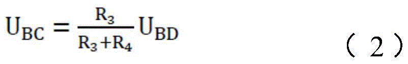
电桥输出的电压U0可表示为The voltage U 0 output by the bridge can be expressed as

在本发明中,R1=R2=R3=R4,将该条件代入式(3),并代带入后所产生的高阶微量忽略以对式(3)进行简化得到:In the present invention, R 1 =R 2 =R 3 =R 4 , this condition is substituted into formula (3), and the high-order trace generated after substituting is ignored to simplify formula (3):

按压作用所产生的电阻变化量与对应电阻的初始电阻值之比与所述电阻受到按压作用后的应变量关系如下:The relationship between the ratio of the resistance variation generated by the pressing action to the initial resistance value of the corresponding resistance and the strain amount of the resistance after the pressing action is as follows:
ΔR/R=Kε (5)ΔR/R=Kε (5)
其中K为电阻的压阻系数。where K is the piezoresistive coefficient of the resistor.
结合上述式(4)与式(5),则U0可进一步表示为:Combining the above formula (4) and formula (5), U0 can be further expressed as:

其中K为电阻的压阻系数,UBD为加载在电性连接点B、D之间的电源VEX大小,ε1,ε2,ε3及ε4一一对应于电阻R1、电阻R2、电阻R3及电阻R4的应变量。Among them, K is the piezoresistive coefficient of the resistor, U BD is the size of the power supply VEX loaded between the electrical connection points B and D, ε 1 , ε 2 , ε 3 and ε 4 correspond to the resistors R 1 and R 2 one by one , The strain of resistance R 3 and resistance R 4 .
通常,我们希望U0输出越大越好,本实施例中,为了获得最大的U0输出值,优选地,压电单元131电极图案如图2B所示。电阻R1、电阻R2、电阻R3及电阻R4均呈方波状,电阻R1和电阻R4形状图案均沿第一方向(X方向)延伸,电阻R2和电阻R3形状图案均沿第二方向(Y方向)延伸,第一方向与第二方向不同。电阻R1、电阻R2、电阻R3及电阻R4通过结合区1311连接形成惠斯通电桥。Generally, we hope that the U 0 output is as large as possible. In this embodiment, in order to obtain the maximum U 0 output value, preferably, the electrode pattern of the
关于电阻的延伸方向界定如下:请参阅图2C,图2C中所示的电阻记为电阻r,其总投影长度包括在第一方向上总投影长度d及在第二方向上总投影长度h。其中,沿第一方向或沿第二方向将所述电阻图案形状分为多段,沿第一方向上的总投影长度d等于线段d1、线段d2、线段d3、线段d4、线段d5及线段d6之和,沿第二方向上总投影长度h等于线段h1、线段h2、线段h3、线段h4及线段h5之和。从图2C可知,沿第一方向上的总投影长度d大于沿第二方向上总投影长度h。因此,电阻r的电极图案形状的延伸方向为第一方向。优选地,电阻r在第一方向上的投影长度大于电阻r在第二方向上的投影长度的5倍。电阻r在其延伸方向上的应变远远大于其他方向发生的应变,因此,可认为电阻r发生的应变近似等于延伸方向上的应变。The extension direction of the resistor is defined as follows: Please refer to FIG. 2C , the resistor shown in FIG. 2C is denoted as resistor r, and its total projected length includes the total projected length d in the first direction and the total projected length h in the second direction. Wherein, the shape of the resistance pattern is divided into multiple sections along the first direction or along the second direction, and the total projection length d along the first direction is equal to the distance between line segment d1, line segment d2, line segment d3, line segment d4, line segment d5 and line segment d6. and, the total projection length h along the second direction is equal to the sum of the line segment h1 , the line segment h2 , the line segment h3 , the line segment h4 and the line segment h5 . It can be seen from FIG. 2C that the total projected length d along the first direction is greater than the total projected length h along the second direction. Therefore, the extension direction of the electrode pattern shape of the resistor r is the first direction. Preferably, the projected length of the resistor r in the first direction is greater than 5 times the projected length of the resistor r in the second direction. The strain of the resistance r in its extension direction is far greater than the strain in other directions, therefore, it can be considered that the strain of the resistance r is approximately equal to the strain in the extension direction.
由于所述电阻R1、电阻R2、电阻R3及电阻R4中的阻值相同,电阻R1和电阻R4形状图案延伸方向一致,电阻R2和电阻R3形状图案延伸方向一致,在四个电阻R1、电阻R2、电阻R3及电阻R4受到的手指按压作用力及温度变化所产生的阻值变化相同的情况下,电阻R1和电阻R4的应变可以认定一致,电阻R2和电阻R3的应变可以认定一致。即电阻R1、电阻R2、电阻R3及电阻R4受到手指按压后产生的应变量之间关系可表示为:ε1=ε4=εx,ε2=ε3=εy,因此,上述式(6)可进一步转化为:Since the resistors R 1 , R 2 , R 3 and R 4 have the same resistance value, the extension direction of the shape pattern of the resistor R 1 and the resistor R 4 is the same, and the extension direction of the shape pattern of the resistor R 2 and the resistor R 3 is the same, In the case that the four resistors R 1 , R 2 , R 3 and R 4 have the same resistance value changes caused by finger pressing force and temperature change, the strains of resistor R 1 and resistor R 4 can be considered to be consistent , the strains of resistor R2 and resistor R3 can be identified as consistent. That is, the relationship among the strains of resistance R 1 , resistance R 2 , resistance R 3 and resistance R 4 after being pressed by a finger can be expressed as: ε 1 = ε 4 = ε x , ε 2 = ε 3 = ε y , so , the above formula (6) can be further transformed into:

εx为电阻R1或电阻R4在第一方向上发生的应变,εy为电阻R1或电阻R4在第二方向上发生的应变。ε x is the strain of the resistor R1 or the resistor R4 in the first direction, and εy is the strain of the resistor R1 or the resistor R4 in the second direction.
从式(2)中可知,当εx和εy的差值越大,U0的输出值越大,压力侦测的灵明度越好。因此,优选第一方向与第二方向垂直。It can be seen from formula (2) that when the difference between ε x and ε y is larger, the output value of U 0 is larger, and the sensitivity of pressure detection is better. Therefore, it is preferable that the first direction is perpendicular to the second direction.
请参阅图2D中所示,作为压感单元131的另一种变形:电桥111b包括四个电阻R1b、电阻R2b、电阻R3b及电阻R4b,该四个电阻的图案形状为椭圆绕线状,该椭圆绕线状的图案形状沿椭圆长轴方向总投影长度最大,则该方向为该图案形状的延伸方向。其中,所述电阻R1b与所述电阻R4b的图案形状的延伸方向与第一方向平行,所述电阻R2b与所述电阻R3b的图案形状的延伸方向与第二方向平行。Please refer to FIG. 2D , as another modification of the pressure-sensitive unit 131: the
本变形实施例中沿第一方向延伸的电阻R1b或电阻R4b的图案形状平面旋转90°后的图案形状与沿第二方向延伸的电阻R2b或电阻R3b的图案形状相同,如此可以保障惠斯特电桥的稳定性的同时可以简化工艺制程。作为一种变形,第一方向延伸的电阻R1b或电阻R4b的图案形状平面旋转90°后的图案形状与沿第二方向延伸的电阻R2b或电阻R3b的图案形状镜像对称。In this variant embodiment, the pattern shape of the resistor R 1b or resistor R 4b extending along the first direction is the same as the pattern shape of the resistor R 2b or resistor R 3b extending along the second direction after the plane is rotated by 90°, so that The process can be simplified while ensuring the stability of the whist bridge. As a modification, the pattern shape of the resistor R 1b or resistor R 4b extending in the first direction is mirror-symmetrical to the pattern shape of the resistor R 2b or resistor R 3b extending in the second direction after the plane is rotated by 90°.
如图2E中所示,作为压感单元131的另一种变形:所述电桥111c包括四个电阻R1c、电阻R2c、电阻R3c及电阻R4c,该四个电阻的图案形状为“栅栏”形折线状,例如可以为“三横一竖”结构,其中,所述电阻R1c与所述电阻R4c的图案形状的延伸方向与第一方向平行,所述电阻R2c与所述电阻R3c的图案形状的延伸方向与第二方向平行。As shown in FIG. 2E , as another modification of the pressure sensing unit 131: the
压感单元131中次压感单元131’的具体形状不做限定,其还可以是波浪形,锯齿形等等。优选,具有第一延伸方向的电阻图案形状平面旋转90°后的图案形状与具有第二延伸方向的电阻图案形状相同或镜像对称。The specific shape of the secondary pressure-sensing unit 131' in the pressure-sensing
与现有技术相比,力感测装置10之力感测层13一侧设置有热处理层17,经过热处理层17的热量分布相对均匀,可有效降低力感测层13上的温度梯度,降低按压力侦测过程产生的温度噪声,提升压力侦测精度。Compared with the prior art, the
请参阅图3,本发明第二实施例力感测装置10a与第一实施例力感测装置10类似,其同样包括基板11a,设置在基板11a上的力感测层13a以及设置在基板11a下方的热处理层17a,力感测层13a包括有多个压感单元131a。本实施例中的力感测装置10a与第一实施例中力感测装置10的不同之处仅在于:力感测装置10a之基板11a与热处理层17a之间通过增设的贴合层15a贴合。基板11a与热处理层17a之间的贴合优选为全贴合。贴合层15a为具有粘性的材料,Please refer to FIG. 3 , the
优选为绝缘光学胶。热处理层17a设置在力感测层13a一侧,具体地,热处理层17a通过贴合层15a固定于基板11a一侧,热处理层17a,基板11a及力感测层13a之间的结合更加紧密,压感单元131a之间的温度梯度进一步减少。It is preferably insulating optical glue. The heat treatment layer 17a is arranged on the side of the
第一实施例中力感测装置10中关于力感测层13的设置,基材11及热处理层17a材料尺寸等参数等的选择等均适应于本实施例。The setting of the
请参阅图4,本发明第三实施例力感测装置10b与第一实施例力感测装置10类似,其同样包括热处理层17b,基板11b以及设置在基板11b上的力感测层13b,该力感测层13b包括有多个压感单元131b。本实施例中的力感测装置10b与第一实施例中力感测装置10的不同之处仅在于:热处理层17b设置在力感测层13b的上方,且力感测层13b通过增设的贴合层15b与热处理层17b贴合,贴合方式优选为全贴合。Please refer to FIG. 4 , the
贴合层15b优选采用绝缘的粘性材料制作,优选为绝缘光学胶。热处理层17b为导电材料时,贴合层15b电性绝缘热处理层17b与力感测层13b。优选贴合层15b的厚度为0.1-1mm,进一步优选为0.4-0.8mm。The
热处理层17b设置在力感测层13b一侧,具体地,热处理层17b通过贴合层15b贴合于力感测层13b一侧,热处理层17b,基板11b及力感测层13b之间的结合紧密,压感单元131b之间的温度梯度减少。The
作为一种变形,所述贴合层15b可以替换为一绝缘层,该绝缘层起绝缘作用,绝缘层叠设在力感测层13b与热处理层17b之间。As a modification, the
作为一种变形,力感测层13b一侧的热处理层17b为多层,多层热处理层17b之间贴合或紧靠叠设。As a modification, the
第一实施例中力感测装置10中关于力感测层13的设置,基材11及热处理层17材料尺寸等参数等的选择等均适应于本实施例。The setting of the
请参阅图5,本发明第四实施例力感测装置10c与第三实施例力感测装置10b类似,其同样包括基板11c以及设置在基板11c上的力感测层13c,该力感测层13c包括有多个压感单元131c。热处理层17c以及贴合层15c设置在力感测层13c上方。本实施例中的力感测装置10c与第三实施例中力感测装置10b的不同之处仅在于:所述力感测层13c上一体成型有一保护层14c,该保护层14c覆盖力感测层13c远离基板11c的表面以对力感测层13c形成保护,防止压感单元131c氧化,被破坏等。热处理层17c通过贴合层15c贴合于保护层14c远离基板11c的表面,贴合方式均优选为全贴合。Please refer to FIG. 5 , the
保护层14c不仅可以保护力感测层13c,还电性隔离了热处理层17c和力感测层13c,其优选采用软质绝缘柔性材料制作,如PEEK(polyetheretherketone,聚醚醚酮),PI(Polyimide,聚酰亚胺),PET(polyethylene terephthalate,聚对苯二甲酸乙二醇酯),PC(聚碳酸酯聚碳酸酯),PES(聚丁二酸乙二醇酯,PMMA(聚甲基丙烯酸甲酯,polymethylmethacrylate)及其任意两者或多者的复合物等材料。The
保护层14c和贴合层15c均可以起到绝缘作用,因此,贴合层15c的厚度可以降低,优选贴合层15c厚度可以是0.01-0.2mm。Both the
第一实施例中力感测装置10中关于力感测层13的设置,基材11及热处理层17材料尺寸等参数等的选择等均适应于本实施例。The setting of the
请参阅图6,本发明第五实施例力感测装置10d与第二实施例力感测装置10a类似,本实施例中的力感测装置10d在第二实施例中力感测装置10a的基础上增设有一热处理层和贴合层,因此,力感测装置10d从上至下依次包括第一热处理层17d,第一贴合层15d,包括多个压感单元131d的力感测层13d,基板11d,第二贴合层15d’以及第二热处理层17d’,基板11d作为力感测层13d的承载层,第一热处理层17d通过第一贴合层15d贴合于力感测层13d的上表面,第二热处理层17d’通过第二贴合层15d’贴合于基板11d的下表面,贴合方式优选为全贴合。Please refer to Fig. 6, the
第一贴合层15d采用绝缘粘性材料制成。第二贴合层15d’采用粘性材料制成,优选采用绝缘粘性材料制成。第一贴合层15d和第二贴合层15d’使得热处理层(包括第一热处理层17d和第二热处理层17d’)与力感测层13d之间的结合更加紧密。The
力感测层13d的两侧均设置有热处理层,热处理层使得来自力感测层13d上下两个表面上的热量分布相对均匀,力感测层13d上的温度梯度进一步减少。Both sides of the
作为一种变形,所述第二贴合层15d’可去除,第二热处理层17d’直接紧靠基板11d下表面叠设。作为又一种变形,所述第一贴合层15d替换为绝缘层,该绝缘层叠设在力感测层13d与第一热处理层17d之间。As a modification, the
作为一种变形,力感测层13d的两侧的热处理层可以有多层。As a variation, the heat treatment layers on both sides of the
第一实施例中力感测装置10中关于力感测层13的设置,基材11及热处理层17材料尺寸等参数等的选择等均适应于本实施例。The setting of the
请参阅图7,本发明第六实施例OLED显示装置20从上至下依次包括盖板22,OLED层24,力感测装置20s以及CPU组件26。Referring to FIG. 7 , an
盖板22的上表面为用户触控操作面,用户在进行触控操作时,其下方设置力感测装置20s,力感测装置20s感测触控操作对应的按压力度。OLED层和力感测装置20s电性连接于CPU组件26,CPU组件26控制OLED显示装置20的运作。The upper surface of the cover plate 22 is a touch operation surface for the user. When the user performs a touch operation, a
力感测装置20s与第二实施例中力感测装置10a结构,材料参数等保持完全一致。同样的,力感测装置20s包括设置有多个压感单元231的力感测层23,力感测层23设置在基板21的一个表面,其另一表面通过贴合层25与热处理层27贴合。力感测层23位于OLED层24和基板21之间。The structure and material parameters of the
最为一种选择,热处理层27为导电材质时,热处理层27接地,热处理层27作为屏蔽层使用以屏蔽来自CPU组件26的干扰信号。该实施方式适用于本发明中的其他实施例。Most alternatively, when the heat treatment layer 27 is made of conductive material, the heat treatment layer 27 is grounded, and the heat treatment layer 27 is used as a shielding layer to shield interference signals from the
可以理解,本实施例中力感测装置20s可以替换为本发明中其他实施例及变形实施例中所揭示的力感测装置。It can be understood that the
CPU组件26为OLED显示装置20的控制中心,其在运作过程中容易产生点热源,热量经过设置在其上方的热处理层27后,热量在热处理层27上分布相对均匀,如此,设置在热处理层27上方的力感测层23受热均匀,温度梯度降减少低,降低按压力侦测过程产生的温度噪声,提升压力侦测精度。可以理解,热处理层27并非只是处理来自CPU组件26的热量,其他任意方向传递过来的热量均能够被热处理层27处理以获得热量均匀分布的特性。The
请参阅图8,本发明第七实施例OLED显示装置20a从上至下依次包括盖板22a,OLED层24a,力感测装置20s’以及CPU组件26a。力感测装置20s’与第二实施例中力感测装置10a结构,材料参数等保持完全一致。同样的,力感测装置20s’包括设置有多个压感单元231a的力感测层23a,力感测层23a设置在基板21a的一个表面,其另一表面通过贴合层25a与热处理层27a贴合。本实施例与第六实施例OLED显示装置20的不同之处仅在于:力感测装置20s’的安装方式不一样,在第六实施例中,力感测层23位于OLED层24和基板21之间,本实施中,力感测装置20s’相当于在平面内旋转了180°进行了安装,因此,力感测层23位于CPU组件26a和基板21之间,热处理层27a设置在OLED层24a与盖板22a之间。Please refer to FIG. 8 , the
可以理解,力感测装置20s’可以替换为本发明中其他实施例及变形实施例中所揭示的力感测装置,且力感测装置可以旋转180°进行两种不同方式的安装。It can be understood that the
请参阅图9,本发明第八实施例OLED显示装置30从上至下依次包括盖板32,触控感测层38,OLED层34,力感测装置30s以及CPU组件36。力感测装置30s与第二实施例中力感测装置10a结构,材料参数等保持完全一致。同样的,力感测装置30s包括设置有多个压感单元331的力感测层33,力感测层33设置在基板31的一个表面,其另一表面通过贴合层35与热处理层37贴合。力感测层33位于OLED层34和基板31之间。Please refer to FIG. 9 , an
本实施例与第六实施例的不同之仅在于在所述盖板32与OLED层34之间增设了触控感测层38,触控感测层38用户感测用户触控位置。界定触控感测层38及盖板32为触控面板,该触控面板可以是OGS触控面板、GFF触控面板、GF触控面板或G2F触控面板,即触控面板为外挂式结构,作为一种变形,其也可以是内嵌式结构,即触控感测层内嵌于OLED层中。The difference between this embodiment and the sixth embodiment is that a
可以理解,力感测装置30s可以替换为本发明中其他实施例及变形实施例中所揭示的力感测装置,且力感测装置可以旋转180°进行两种不同方式的安装。It can be understood that the
与现有技术相比,OLED显示装置30之力感测层33的一侧设置有热处理层37,热处理层37将吸收的热量均匀化以使得力感测层33上的温度梯度减小,降低按压力侦测过程产生的温度噪声,提升压力侦测精度。Compared with the prior art, one side of the
本发明中提供相同尺寸的特制OLED显示装置与本发明中所提供的OLED显示装置(具体为本发明第八实施例中所揭示的OLED显示装置)在不同的温度条件下进行测试。特制的OLED显示装置与本发明中所提供的OLED显示装置的不同之处在于其未设置热处理层,其他配置保持一致。The special OLED display device provided in the present invention with the same size and the OLED display device provided in the present invention (specifically, the OLED display device disclosed in the eighth embodiment of the present invention) were tested under different temperature conditions. The difference between the special OLED display device and the OLED display device provided in the present invention is that no heat treatment layer is provided, and other configurations remain the same.
测试一:Test one:
请参阅图10,以OLED显示装置之显示区域的左下角为原点O建立X,Y坐标系,显示区域尺寸为100mm*60mm,界定显示区域的中心位置为O’点,O’点坐标为(30mm,50mm),在O’点进行触控操作以进行该测试。Please refer to Fig. 10, the X, Y coordinate system is established with the lower left corner of the display area of the OLED display device as the origin O, the size of the display area is 100mm*60mm, the center position of the defined display area is O' point, and the coordinates of O' point are ( 30mm, 50mm), touch operation at O' point for this test.
图11为特制的OLED显示装置与本发明中所提供的OLED显示装置在不同的条件下的测试对比图,该对比图中以OLED显示装置X方向的位置作为横轴,以力感测层上压感单元侦测到的压力值为纵轴。Fig. 11 is a test comparison diagram of a specially made OLED display device and the OLED display device provided in the present invention under different conditions. The pressure value detected by the pressure sensing unit is on the vertical axis.
测试A:Test A:
被测对象:特制的OLED显示装置Tested object: special OLED display device
测试条件:常温的环境下,在O’点施加200单位力;Test conditions: under normal temperature environment, apply 200 units of force at O' point;
测试分析:曲线a1、a2为沿特制的OLED显示装置X方向上的压感单元所侦测到的压力值。其中a1为压感单元中具有第一延伸方向的电阻所侦测到压力值,a2为压感单元中具有第二延伸方向的电阻所侦测到压力值。从曲线走势可看出,特制的OLED显示装置从按压位置处到远离该按压位置处的压感单元所侦测到的压力值逐渐减小。Test analysis: Curves a1 and a2 are the pressure values detected by the pressure-sensitive unit along the X-direction of the specially-made OLED display device. Wherein, a1 is the pressure value detected by the resistor with the first extension direction in the pressure-sensing unit, and a2 is the pressure value detected by the resistor with the second extension direction in the pressure-sensing unit. It can be seen from the trend of the curve that the pressure value detected by the pressure-sensitive unit far away from the pressed position of the special OLED display device gradually decreases from the pressed position.
测试B:Test B:
被测对象:特制的OLED显示装置Tested object: special OLED display device
测试条件:恒定温度65℃,未施加按压力;Test conditions: constant temperature 65°C, no pressing force applied;
测试分析:曲线a3、a4为沿特制的OLED显示装置X方向上的压感单元所侦测到的压力值。其中a3为压感单元中具有第一延伸方向的电阻所侦测到压力值,a4为压感单元中具有第二延伸方向的电阻所侦测到压力值。从曲线走势可看出曲线a3、a4接近横轴,即恒温条件下,压感单元输出几乎为0,也就是压感单元在恒温条件下,温度噪声几乎为0。Test analysis: Curves a3 and a4 are the pressure values detected by the pressure-sensitive unit along the X-direction of the specially-made OLED display device. Wherein, a3 is the pressure value detected by the resistor with the first extension direction in the pressure-sensing unit, and a4 is the pressure value detected by the resistor with the second extension direction in the pressure-sensing unit. It can be seen from the trend of the curves that the curves a3 and a4 are close to the horizontal axis, that is, under the condition of constant temperature, the output of the pressure-sensitive unit is almost 0, that is, the temperature noise of the pressure-sensitive unit is almost 0 under the condition of constant temperature.
测试C:Test C:
被测对象:特制的OLED显示装置Tested object: special OLED display device
测试条件:温度梯度为22℃-65℃,未施加按压力;Test conditions: temperature gradient is 22°C-65°C, no pressing force is applied;
测试分析:曲线a5、a6为沿特制的OLED显示装置X方向上的压感单元所侦测到的压力值。其中a5为压感单元中具有第一延伸方向的电阻所侦测到压力值,a6为压感单元中具有第二延伸方向的电阻所侦测到压力值。从曲线走势可看出虽然无按压力作用于特制的OLED显示装置,但压感单元中具有第一延伸方向的电阻和具有第二延伸方向的电阻所侦测到压力值甚至高于曲线a1,a2中对应的施加200单位力时所侦测到的压力值,即当温度梯度较大时,压感单元所产生了温度噪声非常大,以至于引起较大的压力侦测误差。Test analysis: Curves a5 and a6 are the pressure values detected by the pressure-sensitive unit along the X direction of the specially-made OLED display device. Wherein, a5 is the pressure value detected by the resistor with the first extending direction in the pressure-sensitive unit, and a6 is the pressure value detected by the resistor with the second extending direction in the pressure-sensitive unit. It can be seen from the trend of the curve that although no pressing force acts on the special OLED display device, the pressure values detected by the resistance with the first extension direction and the resistance with the second extension direction in the pressure-sensitive unit are even higher than the curve a1, Corresponding to the pressure value detected when 200 units of force is applied in a2, that is, when the temperature gradient is large, the temperature noise generated by the pressure sensing unit is very large, which causes a large pressure detection error.
测试D:Test D:
被测对象:本发明所提供的OLED显示装置,该OLED显示装置中的热处理层采用石墨烯(石墨烯在热处理层所在平面的导热系数大于等于1000)制作;Tested object: the OLED display device provided by the present invention, the heat treatment layer in the OLED display device is made of graphene (the thermal conductivity of graphene on the plane where the heat treatment layer is located is greater than or equal to 1000);
测试条件:温度梯度为22℃-65℃,未施加按压力;Test conditions: temperature gradient is 22°C-65°C, no pressing force is applied;
测试分析:曲线a7、a8为沿本发明所提供的OLED显示装置X方向上的压感单元所侦测到的压力值。其中a7为压感单元中具有第一延伸方向的电阻所侦测到压力值,a8为压感单元中具有第二延伸方向的电阻所侦测到压力值。从曲线走势可看出曲线a7、a8接近横轴。在增加热处理层的条件下,即使温度梯度较大,压感单元输出几乎为0,也就是压感单元在温度梯度较大的条件下,温度噪声几乎为0。即石墨烯材质制作的热处理层的设置使得压感单元产生的温度噪声降低,压力侦测精度得到了提升。Test analysis: Curves a7 and a8 are the pressure values detected by the pressure sensing unit along the X direction of the OLED display device provided by the present invention. Wherein, a7 is the pressure value detected by the resistor with the first extension direction in the pressure-sensing unit, and a8 is the pressure value detected by the resistor with the second extension direction in the pressure-sensing unit. It can be seen from the trend of the curves that the curves a7 and a8 are close to the horizontal axis. Under the condition of increasing the heat treatment layer, even if the temperature gradient is large, the output of the pressure sensing unit is almost 0, that is, the temperature noise of the pressure sensing unit is almost 0 under the condition of a large temperature gradient. That is, the setting of the heat treatment layer made of graphene material reduces the temperature noise generated by the pressure sensing unit and improves the pressure detection accuracy.
测试E:Test E:
被测对象:本发明所提供的OLED显示装置,该OLED显示装置中的热处理层采用石墨片(石墨片在热处理层所在平面的导热系数大于等于200)制作;Tested object: the OLED display device provided by the present invention, the heat treatment layer in the OLED display device is made of graphite sheet (the thermal conductivity of the graphite sheet on the plane where the heat treatment layer is located is greater than or equal to 200);
测试条件:温度梯度为22℃-65℃,未施加按压力;Test conditions: temperature gradient is 22°C-65°C, no pressing force is applied;
测试分析:曲线a9、a10为沿本发明所提供的OLED显示装置X方向上的压感单元所侦测到的压力值。其中a9为压感单元中具有第一延伸方向的电阻所侦测到压力值,a10为压感单元中具有第二延伸方向的电阻所侦测到压力值。从曲线走势可看出曲线a9、a10接近横轴。在增加热处理层的条件下,即使温度梯度较大,压感单元输出几乎为0,也就是压感单元在温度梯度较大的条件下,温度噪声几乎为0。即石墨片材质的热处理层的设置使得压感单元产生的温度噪声降低,压力侦测精度得到了提升。Test analysis: Curves a9 and a10 are the pressure values detected by the pressure sensing unit along the X direction of the OLED display device provided by the present invention. Wherein, a9 is the pressure value detected by the resistor with the first extension direction in the pressure-sensing unit, and a10 is the pressure value detected by the resistor with the second extension direction in the pressure-sensing unit. It can be seen from the trend of the curves that the curves a9 and a10 are close to the horizontal axis. Under the condition of increasing the heat treatment layer, even if the temperature gradient is large, the output of the pressure sensing unit is almost 0, that is, the temperature noise of the pressure sensing unit is almost 0 under the condition of a large temperature gradient. That is, the setting of the heat treatment layer made of graphite sheet reduces the temperature noise generated by the pressure sensing unit and improves the pressure detection accuracy.
测试F:Test F:
被测对象:本发明所提供的OLED显示装置,该OLED显示装置中的热处理层采用铁片制作,该导热片在热处理层所在平面的导热系数约为70;Tested object: the OLED display device provided by the present invention, the heat treatment layer in the OLED display device is made of iron sheet, and the thermal conductivity of the heat conduction sheet is about 70 on the plane where the heat treatment layer is located;
测试条件:温度梯度为22℃-65℃,未施加按压力;Test conditions: temperature gradient is 22°C-65°C, no pressing force is applied;
测试分析:曲线a11、a12为沿本发明所提供的OLED显示装置X方向上的压感单元所侦测到的压力值。其中a11为压感单元中具有第一延伸方向的电阻所侦测到压力值,a12为压感单元中具有第二延伸方向的电阻所侦测到压力值。从曲线走势可看出具有第一延伸方向的电阻所侦测到压力值约200单位力,具有第二延伸方向的电阻所侦测到压力值约100单位力。即温度梯度为22℃-65℃下,压感单元仍然产生了温度噪声。但与测试C相比可知,热处理层的设置在一定程度上抑制了温度噪声的产生。与测试D、E相比可知,热处理层在使用石墨烯材质制作时,抑制了温度噪声的产生效果最佳。Test analysis: Curves a11 and a12 are the pressure values detected by the pressure-sensitive unit along the X direction of the OLED display device provided by the present invention. Wherein, a11 is the pressure value detected by the resistor with the first extension direction in the pressure-sensing unit, and a12 is the pressure value detected by the resistor with the second extension direction in the pressure-sensing unit. It can be seen from the trend of the curve that the resistance with the first extension direction detects a pressure value of about 200 unit force, and the resistance with the second extension direction detects a pressure value of about 100 unit force. That is, when the temperature gradient is 22°C-65°C, the pressure sensing unit still generates temperature noise. However, compared with test C, it can be seen that the setting of the heat treatment layer suppresses the generation of temperature noise to a certain extent. Compared with tests D and E, it can be seen that when the heat treatment layer is made of graphene material, the effect of suppressing the generation of temperature noise is the best.
测试二:Test two:
用吹风将特制的OLED显示装置与本发明中所提供的OLED显示装置从室温加热到95°,重复试验5次,现有的OLED显示装置与本实施例中所提供的OLED显示装置压力感测的输出变化如下:Heat the specially-made OLED display device and the OLED display device provided in the present invention from room temperature to 95° with a blower, and repeat the test 5 times. The pressure sensing of the existing OLED display device and the OLED display device provided in this embodiment The output changes as follows:
表1特制的OLED显示装置与本发明中OLED显示装置受热后压力感测信号输出对比测试Table 1 Comparison test of pressure sensing signal output between the specially made OLED display device and the OLED display device of the present invention after heating

从上表中可看出,在温度急剧变化的情况下,特制的OLED显示装置之压感单元的输出信号明显大于本发明中提供的OLED显示装置之压感单元输出信号。而本发明中提供的OLED显示装置的输出信号基本趋于稳定。可见,增设有热处理层的OLED显示装置之力感测层的温度噪声降低,压力侦测精度得到了提升。It can be seen from the above table that the output signal of the pressure-sensing unit of the special OLED display device is significantly larger than that of the pressure-sensing unit of the OLED display device provided in the present invention in the case of a sharp temperature change. However, the output signal of the OLED display device provided in the present invention tends to be basically stable. It can be seen that the temperature noise of the force sensing layer of the OLED display device with the added heat treatment layer is reduced, and the pressure detection accuracy is improved.
以上所述仅为本发明的较佳实施例而已,并不用以限制本发明,凡在本发明的原则之内所作的任何修改,等同替换和改进等均应包含本发明的保护范围之内。The above descriptions are only preferred embodiments of the present invention, and are not intended to limit the present invention. Any modifications, equivalent replacements and improvements within the principles of the present invention shall be included within the protection scope of the present invention.
Claims (20)
Priority Applications (4)
| Application Number | Priority Date | Filing Date | Title |
|---|---|---|---|
| CN201710029471.9A CN106598347B (en) | 2017-01-16 | 2017-01-16 | Force sensing device and OLED display device |
| TW106140786A TWI736711B (en) | 2017-01-16 | 2017-11-23 | Force sensor device and oled display device including the same |
| TW106217444U TWM563004U (en) | 2017-01-16 | 2017-11-23 | Force sensing device and OLED display device including force sensing device |
| US15/872,916 US10553655B2 (en) | 2017-01-16 | 2018-01-16 | Force sensor device and OLED display device including the same |
Applications Claiming Priority (1)
| Application Number | Priority Date | Filing Date | Title |
|---|---|---|---|
| CN201710029471.9A CN106598347B (en) | 2017-01-16 | 2017-01-16 | Force sensing device and OLED display device |
Publications (2)
| Publication Number | Publication Date |
|---|---|
| CN106598347A CN106598347A (en) | 2017-04-26 |
| CN106598347B true CN106598347B (en) | 2023-04-28 |
Family
ID=58585876
Family Applications (1)
| Application Number | Title | Priority Date | Filing Date |
|---|---|---|---|
| CN201710029471.9A Active CN106598347B (en) | 2017-01-16 | 2017-01-16 | Force sensing device and OLED display device |
Country Status (3)
| Country | Link |
|---|---|
| US (1) | US10553655B2 (en) |
| CN (1) | CN106598347B (en) |
| TW (2) | TWM563004U (en) |
Families Citing this family (10)
| Publication number | Priority date | Publication date | Assignee | Title |
|---|---|---|---|---|
| CN106598347B (en) * | 2017-01-16 | 2023-04-28 | 宸鸿科技(厦门)有限公司 | Force sensing device and OLED display device |
| CN106951127A (en) * | 2017-05-04 | 2017-07-14 | 宸鸿科技(厦门)有限公司 | Pressure-sensing module, contactor control device and OLED display |
| CN107256101B (en) * | 2017-06-30 | 2020-05-12 | 上海天马微电子有限公司 | Touch display panel and display device |
| KR102343734B1 (en) * | 2017-07-12 | 2021-12-28 | 삼성디스플레이 주식회사 | Display device |
| CN107463020B (en) * | 2017-08-30 | 2020-07-07 | 厦门天马微电子有限公司 | A display substrate, a display panel and a display device |
| CN107589872A (en) * | 2017-09-20 | 2018-01-16 | 厦门天马微电子有限公司 | A kind of display panel and display device |
| CN109727532A (en) * | 2017-10-30 | 2019-05-07 | 京东方科技集团股份有限公司 | Flexible display and display device |
| CN110830639B (en) * | 2019-10-28 | 2021-10-01 | 维沃移动通信有限公司 | an electronic device |
| WO2021102219A1 (en) * | 2019-11-22 | 2021-05-27 | Corning Incorporated | Laminate with integral force sensor and related methods |
| US11269440B1 (en) * | 2020-08-12 | 2022-03-08 | Universal Cement Corporation | Foldable force sensing device |
Citations (2)
| Publication number | Priority date | Publication date | Assignee | Title |
|---|---|---|---|---|
| CN204405992U (en) * | 2015-03-03 | 2015-06-17 | 信利半导体有限公司 | A kind of LCDs |
| CN105224129A (en) * | 2015-09-01 | 2016-01-06 | 宸鸿科技(厦门)有限公司 | A kind of pressure-sensing input media |
Family Cites Families (10)
| Publication number | Priority date | Publication date | Assignee | Title |
|---|---|---|---|---|
| US8957577B2 (en) * | 2011-09-30 | 2015-02-17 | Apple Inc. | Integrated thermal spreading |
| AU2015100011B4 (en) * | 2014-01-13 | 2015-07-16 | Apple Inc. | Temperature compensating transparent force sensor |
| US9542056B2 (en) * | 2014-05-20 | 2017-01-10 | Uneo Incorporated | Resistive force sensing circuit |
| EP3180376A1 (en) * | 2014-08-15 | 2017-06-21 | H. B. Fuller Company | Re-workable moisture curable hot melt adhesive composition methods of using the same, and articles including the same |
| JP6400108B2 (en) * | 2014-08-26 | 2018-10-03 | 三菱電機株式会社 | High frequency module |
| KR102395602B1 (en) * | 2015-06-30 | 2022-05-09 | 엘지디스플레이 주식회사 | Electronic device having force touch function |
| CN106325582B (en) * | 2015-07-10 | 2023-07-28 | 宸鸿科技(厦门)有限公司 | A touch assembly with pressure detection and its driving method |
| CN106325583B (en) * | 2015-07-10 | 2023-10-10 | 宸鸿科技(厦门)有限公司 | pressure sensing input device |
| KR102606498B1 (en) * | 2016-08-29 | 2023-11-27 | 엘지전자 주식회사 | Mobile terminal |
| CN106598347B (en) * | 2017-01-16 | 2023-04-28 | 宸鸿科技(厦门)有限公司 | Force sensing device and OLED display device |
-
2017
- 2017-01-16 CN CN201710029471.9A patent/CN106598347B/en active Active
- 2017-11-23 TW TW106217444U patent/TWM563004U/en unknown
- 2017-11-23 TW TW106140786A patent/TWI736711B/en active
-
2018
- 2018-01-16 US US15/872,916 patent/US10553655B2/en active Active
Patent Citations (2)
| Publication number | Priority date | Publication date | Assignee | Title |
|---|---|---|---|---|
| CN204405992U (en) * | 2015-03-03 | 2015-06-17 | 信利半导体有限公司 | A kind of LCDs |
| CN105224129A (en) * | 2015-09-01 | 2016-01-06 | 宸鸿科技(厦门)有限公司 | A kind of pressure-sensing input media |
Also Published As
| Publication number | Publication date |
|---|---|
| US10553655B2 (en) | 2020-02-04 |
| CN106598347A (en) | 2017-04-26 |
| TWM563004U (en) | 2018-07-01 |
| TW201828467A (en) | 2018-08-01 |
| TWI736711B (en) | 2021-08-21 |
| US20180204885A1 (en) | 2018-07-19 |
Similar Documents
| Publication | Publication Date | Title |
|---|---|---|
| CN106598347B (en) | Force sensing device and OLED display device | |
| TWI663386B (en) | Pressure sensor and display device | |
| US10452215B2 (en) | Mutual capacitive force sensor and touch display device with force sensing function and force sensing method thereof | |
| CN105426005B (en) | three-dimensional touch panel | |
| CN106249953B (en) | A kind of pressure sensitivity touch screen and display device | |
| CN107111404A (en) | Combined sensor system | |
| CN205158318U (en) | Touch display device | |
| CN104951087A (en) | Information processing device, input device, information processing method, and program | |
| KR20140006062A (en) | Capacitive touch panel and a method of manufacturing the same | |
| TWI579756B (en) | Three-dimensional input module | |
| CN103336603A (en) | touch display device | |
| US8564542B2 (en) | Multi-touch detecting method for detecting locations of touched points on a touch panel | |
| CN204833200U (en) | Contactor control device | |
| CN204808289U (en) | Touch -sensitive screen and display device | |
| CN105589603A (en) | Touch structure, touch display panel and touch display device | |
| CN107422904A (en) | Touch-screen and electronic equipment | |
| CN102621728B (en) | Touch device with shielding layer | |
| US10345952B2 (en) | Touch panel | |
| CN107918502A (en) | Mutual capacitance type pressure sensor, touch display device and pressure sensing method thereof | |
| TWI538025B (en) | Touch electrode structure and manufacturing method thereof | |
| TW201804307A (en) | Capacitive pressure-sensitive display apparatus | |
| CN206515803U (en) | Power sensing device further and OLED display | |
| CN107562245A (en) | Touch display unit and electronic equipment | |
| TW201435678A (en) | Touch sensor with cover lens | |
| TWI679572B (en) | Touch electrode pattern and touch display device using the same |
Legal Events
| Date | Code | Title | Description |
|---|---|---|---|
| PB01 | Publication | ||
| PB01 | Publication | ||
| SE01 | Entry into force of request for substantive examination | ||
| SE01 | Entry into force of request for substantive examination | ||
| GR01 | Patent grant | ||
| GR01 | Patent grant |