The present application is a divisional application of an invention patent application having an application date of 2012, 3/7, application number of 201210058232.3, entitled "element of solid-state imaging device, manufacturing method of solid-state imaging device, and electronic apparatus".
Detailed Description
(first embodiment)
Fig. 1 is a schematic block diagram showing an exemplary solid-state imaging device 100 according to a first embodiment of the present technology. The solid-state imaging device 100 shown in fig. 1 includes a substrate 111 made of silicon, a pixel portion 113 including a plurality of pixels 112 arranged in an array on the substrate 111, a vertical driving circuit 114, a column signal processing circuit 115, a horizontal driving circuit 116, an output circuit 117, and a control circuit 118.
The pixel section 113 includes a plurality of pixels 112 regularly arranged in a two-dimensional array. The pixel section 113 includes an effective pixel region that actually receives incident light, amplifies signal charges generated by photoelectric conversion of the incident light, and outputs the amplified signal charges to the column signal processing circuit 115, and a black reference pixel region (not shown) for outputting optical black (optical black) to serve as a reference black level. The black reference pixel region is generally formed at the periphery of the effective pixel region.
The pixel 112 includes a photodiode as a photoelectric conversion element (not shown) and a plurality of pixel transistors (not shown). A plurality of pixels 112 are regularly arranged in a two-dimensional array on a substrate 111. The plurality of pixel transistors may include four kinds of MOS transistors including a transfer transistor, a reset transistor, a selection transistor, and an amplification transistor, or may include the above three kinds of transistors except for the selection transistor.
The control circuit 118 generates a clock signal and a control signal for use as reference signals for the operation of the vertical drive circuit 114, the column signal processing circuit 115, and the horizontal drive circuit 116, based on the vertical synchronization signal, the horizontal synchronization signal, and the master clock. The control circuit 118 controls the vertical drive circuit 114, the column signal processing circuit 115, and the horizontal drive circuit 116 with a clock signal and a control signal.
The vertical drive circuit 114 is formed of, for example, a shift register, and selectively scans the pixels 112 row by row sequentially in the vertical direction. The vertical drive circuit 114 supplies a pixel signal based on signal charges generated in accordance with the amount of light received by the photoelectric conversion element of the pixel 112 to the column signal processing circuit 115 through the vertical signal line 119.
The column signal processing circuit 115 corresponds to, for example, a column of the pixels 112, and performs signal processing such as noise reduction of the relevant pixel column and signal amplification of signals output from one row of the pixels 112 in accordance with signals from the black reference pixel region. A horizontal selection switch (not shown) is provided between the output stage of the column signal processing circuit 115 and the horizontal signal line 120.
The horizontal drive circuit 116 is formed of, for example, a shift register. The horizontal drive circuit 116 sequentially outputs horizontal scan pulses to sequentially select the column signal processing circuits 115, and causes each of the column signal processing circuits 115 to output a pixel signal to the horizontal signal line 120.
The output circuit 117 processes pixel signals sequentially supplied from the column signal processing circuit 115 through the horizontal signal line 120, and outputs the processed signals to an external device (not shown).
Referring now to fig. 2, the solid-state imaging device 100 will be described in detail.
As shown in fig. 2, the solid-state imaging device 100 according to the present embodiment includes a substrate 111, a wiring layer 26 formed on the front side of the substrate 111, a support substrate 14, a color filter 15 formed on the rear side of the substrate 111 with an insulating film 18 therebetween, and a microlens 16.
The substrate 111 is a semiconductor substrate made of silicon. The thickness of the substrate 111 is 3-5 μm. On the substrate 111, a plurality of pixels 112 each including the photoelectric conversion element 11 and a plurality of pixel transistors Tr forming a pixel circuit portion are formed in a two-dimensional matrix. Although not shown in fig. 2, a peripheral circuit portion is formed in a peripheral region of the pixel 112 formed on the substrate 111.
In the photoelectric conversion element 11, which is, for example, a photodiode, signal charges are generated according to the amount of light received from incident light and are accumulated.
The pixel transistor Tr has a source/drain region (not shown) formed on the front side of the substrate 111 and a gate electrode 128 formed on the front side of the substrate 11 with a gate insulating film 129 therebetween.
An element isolation region 24 including a high-concentration impurity region is formed between adjacent pixels 112, and extends from the front side to the back side of the substrate 111. The pixels 112 are electrically isolated from each other by the element isolation region 24.
The wiring layer 26 is formed on the front side of the substrate 111, and has wirings 261 provided in multiple layers (three layers in fig. 2) with interlayer insulator films 27 therebetween. The formation portion of the pixel transistor Tr of the pixel 112 is driven through the wiring 261 formed in the wiring layer 26.
The support substrate 14 is formed on a surface of the wiring layer 26 opposite to a surface facing the substrate 111. The support substrate 14 is formed to secure the strength of the substrate 111 at the manufacturing stage. The support substrate 14 is formed of, for example, a silicon substrate.
The color filter 15 is formed on the rear side of the substrate 111 with the insulator film 18 between the color filter 15 and the substrate 111, and includes, for example, first, second, and third color filter components for each pixel. For example, the first, second and third color filter components may be green, red and blue filter components, respectively, but are not limited thereto, and may be filter components of any color. Instead of the color filter member, other filter members may be used, for example, a transparent resin that transmits visible light or an ND filter that includes a carbon black pigment in the transparent resin to attenuate visible light.
Light of a desired wavelength is transmitted through the color filter 15 and enters the photoelectric conversion element 11 in the substrate 111.
The light shielding film 17 is provided between the color filter components of the color filter 15. Adhesive films 19 are formed between the light-shielding film 17 and the color filters 15 and between the insulator film 18 and the color filters 15.
The light-shielding film 17 is provided to reduce color mixing caused by leakage of incident light to the adjacent photoelectric conversion elements 11. The light shielding film 17 is formed of a conductive material or an organic material in which a black material is dispersed.
In order to adhere the color filter 15 to the light-shielding film 17 and the insulator film 18, an adhesive film 19 is provided between the color filter 15 and the light-shielding film 17 and the insulator film 18. The adhesive film 19 is a non-flat transparent film and has good adhesion to a color filter, an oxide film, a nitride film, and a metal. Preferably, the adhesive film 19 is made of a thermoplastic resin material having thermal fluidity in a certain temperature range so as to reduce coating irregularities due to the rough surface of the lower layer in a heat-acting process and having thermosetting properties in a final heat-treating process.
Examples of the resin material include organic films such as acrylic resins, phenol resins, silicone resins or copolymer resins thereof, and epoxy resins. More specifically, for example, "TMR-C006" available from TOKYO OHKA KOGYO co. The epoxy resin may be applied to a curable base or a curing agent. As the binder film 19, an insulating film containing Si (silicon element), C (carbon element), and H (hydrogen element) as main components, for example, a single inorganic film such as SiCH, SiCOH, and SiCNH can be used.
The adhesive film 19 is formed by utilizing the shape of the light shielding film 17. More specifically, since the adhesive film 19 is deposited after the light shielding film 17 is formed, the adhesive film 19 is formed on the upper surface and the side wall of the light shielding film 17.
The
adhesive film 19 has a thickness that can be formed at a position lower than the light-shielding
film 17 formed corresponding to each pixel by at least a part of the
color filter 15. That is, when the film thickness of the light-shielding
film 17 is T1, the film thickness T2 of the
adhesive film 19 satisfies the requirement
Note that the
adhesive film 19 is formed by patterning and etching using a photolithography technique so as to cover only the upper surface and the side wall of the
light shielding film 17.
Next, a manufacturing method of the solid-state imaging device 100 will be described. The manufacturing method of the solid-state imaging device 100 includes: the method includes forming pixels 112 each having a photoelectric conversion element 11 for converting incident light into an electric signal, forming a light-shielding film 17 to be disposed between a plurality of color filter components of a color filter 15, depositing a non-flat adhesive film 19 on the light-shielding film 17, forming the color filter 15 on the adhesive film 19 between the light-shielding films 17, and forming a micro lens 16 on the color filter 15 to condense the incident light onto the photoelectric conversion element 11 through the color filter 15.
Referring now to fig. 3A to 3F, a method of manufacturing the solid-state imaging device 100 will be described in detail. The formation steps of the pixel 112 are similar to those of the related art, and thus a description thereof will be omitted.
As shown in fig. 3A, the insulator film 18 is deposited on the photoelectric conversion element 11 by CVD, ALD, PVD, or the like.
Next, a film 171 (in this case, metal) is deposited to form a light-shielding film 17 (fig. 3B). Subsequently, the film 171 is patterned by photolithography to form holes for the pixels 112 in the film 171, and then the light-shielding film 17 is formed by etching (fig. 3C).
As shown in fig. 3D, after the light shielding film 17 is formed, an adhesive film 19 is deposited or coated using a spin coating process, a spray coating process, a slit coating (slit coating) process, or the like. An optically effective color filter 15 having a thickness of about 100nm to 1 μm is formed on the adhesive film 19 (fig. 3E).
The micro lens 16 is formed on the color filter 15 (fig. 3F).
In the solid-state imaging device 100 according to the present embodiment, the uneven adhesive film 19 provided between the color filter 15 and the light-shielding film 17 as described above can suppress separation of the color filter.
In addition, since a part of the color filter 15 is embedded in the layer of the light-shielding film 17, it is possible to reduce the height of the solid-state imaging device 100. Thereby enabling a reduction in color mixing and an improvement in sensitivity of the solid-state imaging device 300. Further, the color filter 15 can be formed by self-alignment based on the light shielding film 17 formed between the pixels, and the overlapping accuracy of the light shielding film 17 and the color filter 15 can be improved.
(second embodiment)
Next, a solid-state imaging device 200 according to a second embodiment will be described. Since the solid-state imaging device 200 has the same configuration as the solid-state imaging device 100 in fig. 2 except for the flat color filter 25, the same components are denoted by the same reference numerals, and the description thereof will be omitted.
The solid-state imaging device 200 shown in fig. 4 has the color filter 25 disposed in the same layer as the light-shielding film 17 and the adhesive film 29 formed on the side wall of the light-shielding film 17 and on the insulator film 18.
An adhesive film 29 is formed between the light shielding film 17 and the color filter 25. The adhesive film 29 is formed on a side wall of the light shielding film 17, but is not formed on one surface perpendicular to the side wall of the light shielding film 17. An adhesive film 29 is also formed on the insulator film 18. The structure and material of the adhesive film 29 are the same as those of the adhesive film 19 in fig. 2, except for the shape of the adhesive film 29.
The color filter 25 is planarized and formed in the same layer as the light-shielding film 17.
The solid-state imaging device 200 has an adhesive film 29 and a color filter 25, which are sequentially formed in a hole formed by the light-shielding film 17 and the insulator film 18. The adhesive film 29 is formed not only between the color filter 25 and the insulator film 18 but also between the side wall of the light-shielding film 17 and the color filter 25.
Next, a manufacturing method of the solid-state imaging device 200 will be described. The steps up to the formation of the color filter 25 are the same as those shown in fig. 3A to 3E, and thus the description thereof is omitted.
In fig. 3A to 3F, the color filter 15 is formed before the microlens 16 is formed. In the present embodiment, alternatively, the color filter 25 is formed and planarized before the formation of the micro lenses 16, as shown in fig. 5A and 5B.
As shown in fig. 5A, after the color filter 25 is formed, the color filter 25 is planarized by CMP, dry etching, or the like. Here, the color filter 25 is planarized to expose the surface of the light shielding film 17. The adhesive film 29 formed on one surface of the light shielding film 17 is also etched accordingly. Alternatively, the etching may be stopped while the adhesive film 29 remains. In this case, the adhesive film 29 will be formed on the side wall of the light-shielding film 17 and on the insulator film 18.
As shown in fig. 5B, after planarizing the color filter 25, the micro-lenses 16 are formed on the color filter 25.
As described above, the solid-state imaging device 200 according to the present embodiment can improve imaging quality to have improved irregularity/shading/sensitivity ratio due to the planarized color filter 25, and can suppress separation of the color filter by the adhesive film 29 provided between the color filter 25 and the light shielding film 17 and between the color filter 25 and the insulator film 18. Further, since a part of the color filter 25 is embedded in the layer of the light shielding film 17, it is possible to reduce the height of the solid-state imaging device 100. Further, the color filter 25 can be formed by self-alignment based on the light-shielding film 17 formed between the pixels, and the overlapping accuracy of the light-shielding film 17 and the color filter 25 can be improved.
(third embodiment)
Next, a solid-state imaging device 300 according to a third embodiment will be described. Since the solid-state imaging device 300 has the same configuration as the solid-state imaging device 100 in fig. 2 except for the shape of the adhesive film 39, the same components are denoted by the same reference numerals, and description thereof is omitted.
The solid-state imaging device 300 shown in fig. 6 has an adhesive film 39 formed between one surface of the light shielding film 17 and the color filter 15.
The adhesive film 39 is formed on a part of the light-shielding film 17, i.e., one surface thereof in this embodiment, and is not formed on the side wall of the light-shielding film 17 and on the insulator film 18. The material and other features of the adhesive film 39 are the same as those of the adhesive film 19 shown in fig. 2, and thus the description thereof is omitted.
Next, a manufacturing method of the solid-state imaging device 300 will be described. The steps up to the formation of the film 171 are the same as those in fig. 3A and 3B, and thus the description thereof is omitted.
After forming the film 171, an adhesive film 39 is deposited on the film 171, as shown in fig. 7A. Subsequently, the film 171 is patterned by photolithography to form holes for the pixels 112 in the film 171, and then the film 171 and the adhesive film 39 are etched to form the light-shielding film 17 and the adhesive film 39 (fig. 7B).
Next, the color filter 15 is formed (fig. 7C), and the micro-lenses 16 are formed on the color filter 15 (fig. 7D).
Since the adhesive film 39 is not provided between the insulator film 18 and the color filter 15 as described above, the solid-state imaging device 300 according to the present embodiment can be reduced in height as compared with the solid-state imaging device 100 shown in fig. 2. For this reason, the solid-state imaging device 300 can achieve a reduction in color mixing and improve sensitivity. The adhesive film 39 provided between one surface of the light-shielding film 17 and the color filter 15 can suppress separation of the color filter. Further, the color filter 15 can be formed by self-alignment based on the light shielding film 17 formed between the pixels, and the overlapping accuracy of the light shielding film 17 and the color filter 15 can be improved.
The solid-state imaging device 300 according to the present embodiment is particularly useful when the adhesion of the light-shielding film 17 to the color filter 15 is lower than the adhesion of the insulator film 18 to the color filter 15.
(fourth embodiment)
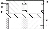
Next, a solid-state imaging device 400 according to a fourth embodiment will be described. Since the solid-state imaging device 400 has the same configuration as the solid-state imaging device 100 in fig. 2 except for the shape of the insulating film 48, the same components are denoted by the same reference numerals, and description thereof is omitted.
As shown in fig. 8, the solid-state imaging device 400 includes the insulator film 48 having a recess.
The insulator film 48 has projections and depressions on one surface. The light shielding film 17 is formed on the projection, and the adhesive film 19 and the color filter 15 are formed in the recess. Thus, the solid-state imaging device 400 has the adhesive film 19 and the color filter 15 embedded in the insulator film 48.
Next, a manufacturing method of the solid-state imaging device 400 will be described. The steps up to the formation of the film 171 are the same as those in fig. 3A and 3B, and thus the description thereof is omitted.
After the film 171 is formed, the film 171 is patterned by photolithography to form holes for the pixels 112 in the film 171, and then the film 171 and the insulator film 48 are etched as shown in fig. 9A. The total etching depth of the light-shielding film 17 and the insulator film 48 is about 100nm to 1 μm. Thus, the insulator film 48 and the light-shielding film 17 having the depressions are formed.
After the light shielding film 17 is formed, an adhesive film 19 is deposited or coated using a spin coating process, a spray coating process, a slit coating process, or the like, as shown in fig. 9B. Then, a color filter 15 having a thickness of about 100nm to 1 μm is formed (fig. 9C), and a microlens 16 is formed on the color filter 15 (fig. 9D).
As described above, the solid-state imaging device 400 according to the present embodiment has the insulator film 48 with the recess and the color filter 15 embedded in the recess. This allows the solid-state imaging device 400 to be reduced in height while maintaining the color filter 15 of a desired thickness without increasing the thickness of the light shielding film 17. For this reason, the solid-state imaging device 400 can achieve a reduction in color mixing and improve sensitivity. The adhesive film 19 provided between the light-shielding film 17 and the color filter 15 can suppress separation of the color filter 15. Further, the color filter 15 can be formed by self-alignment based on the light shielding film 17 formed between the pixels, and the overlapping accuracy of the light shielding film 17 and the color filter 15 can be improved.
To etch the insulator film 48 in fig. 9A, isotropic etching may be employed to form circular recesses in the insulator film 48. In this case, the optical waveguide formed by the light-shielding film 17 and the adhesive film 19 will form a convex lens protruding downward at the lower portion thereof, which causes the incident light from the microlens 16 to be further condensed.
(fifth embodiment)
Next, a solid-state imaging device 500 according to a fifth embodiment will be described. Since the solid-state imaging device 500 has the same configuration as the solid-state imaging device 400 in fig. 8 except for the planarized color filter 25, the same components are denoted by the same reference numerals, and the description thereof is omitted.
The solid-state imaging device 500 shown in fig. 10 has the color filter 25 provided in the same layer as the light-shielding film 17 and the adhesive film 29 formed on the side wall of the light-shielding film 17 and on the insulator film 18.
An adhesive film 29 is formed between the light shielding film 17 and the color filter 25. The adhesive film 29 is formed on a side wall of the light shielding film 17, but is not formed on one surface of the light shielding film 17 perpendicular to the side wall. An adhesive film 29 is also formed on the insulator film 18. The structure and material of the adhesive film 29 are the same as those of the adhesive film 19 in fig. 2, except for the shape of the adhesive film 29.
The color filter 25 is planarized and formed in the same layer as the light-shielding film 17.
The solid-state imaging device 500 has an adhesive film 29 and a color filter 25, which are sequentially formed in a hole formed by the light-shielding film 17 and the insulator film 18. The adhesive film 29 is formed not only between the color filter 25 and the insulator film 18 but also between the side wall of the light-shielding film 17 and the color filter 25.
Next, a manufacturing method of the solid-state imaging device 500 will be described. The steps up to forming the color filter 25 are the same as those in fig. 9A to 9C, and thus the description thereof is omitted.
In fig. 9A to 9D, after the color filter 15 is formed, the micro lens 16 is formed. In the present embodiment, alternatively, before the micro lenses 16 are formed, the planarization color filter 25 is formed and planarized as shown in fig. 11A and 11B.
As shown in fig. 11A, after the color filter 25 is formed, the color filter 25 is planarized by CMP, dry etching, or the like. Here, the color filter 25 is planarized to expose the surface of the light shielding film 17 as shown in fig. 11A. The adhesive film 29 formed on one surface of the light shielding film 17 is also etched accordingly. Alternatively, the etching may be stopped while the adhesive film 29 remains. In this case, the adhesive film 29 will be formed on the side wall of the light-shielding film 17 and on the insulator film 18.
As shown in fig. 11B, after planarizing the color filter 25, the micro-lenses 16 are formed on the color filter 25.
As described above, according to the solid-state imaging device 500 of the present embodiment, due to the planarized color filter 25, the image quality can be improved to have an improved irregularity/shading/sensitivity ratio or the like, and separation of the color filter can be suppressed by the adhesive film 29 provided between the color filter 25 and the light shielding film 17 and between the color filter 25 and the insulator film 18. Further, the color filter 25 can be formed by self-alignment based on the light-shielding film 17 formed between the pixels, and the overlapping accuracy of the light-shielding film 17 and the color filter 25 can be improved.
(sixth embodiment)
Next, a solid-state imaging device 600 according to a sixth embodiment will be described. Since the solid-state imaging device 600 has the same configuration as the solid-state imaging device 400 in fig. 8 except for the shape of the adhesive 39, the same components are denoted by the same reference numerals, and description thereof is omitted.
The solid-state imaging device 600 shown in fig. 12 has an adhesive film 39 formed between one surface of the light shielding film 17 and the color filter 15.
The adhesive film 39 is formed on a part of the light-shielding film 17, i.e., one surface thereof in the present embodiment, but is not formed on the side wall of the light-shielding film 17 and on the insulator film 18. The material and other features of the adhesive film 39 are the same as those of the adhesive film 19 shown in fig. 2, and thus the description thereof is omitted.
Next, a manufacturing method of the solid-state imaging device 600 will be described. The steps up to depositing the adhesive film 39 on the film 171 are the same as those shown in fig. 7A, and thus the description thereof is omitted.
After the adhesive film 39 is formed, the film 171 is patterned by photolithography to form holes for the pixels 112 in the film 171, and then the film 171 and the insulator film 48 are etched as shown in fig. 13A. Then, a color filter 15 having a thickness of about 100nm to 1 μm is formed (fig. 13B), and a microlens 16 is formed on the color filter 15 (fig. 13C).
Since the adhesive film 39 is not provided between the insulator film 18 and the color filter 15 as described above, the solid-state imaging device 600 according to the present embodiment can be reduced in height as compared with the solid-state imaging device 400 shown in fig. 8. For this reason, the solid-state imaging device 600 can achieve reduction in color mixing and improvement in sensitivity. The adhesive film 39 provided between one surface of the light-shielding film 17 and the color filter 15 can suppress separation of the color filter. Further, the color filter 15 can be formed by self-alignment based on the light shielding film 17 formed between the pixels, and the overlapping accuracy of the light shielding film 17 and the color filter 15 can be improved.
The solid-state imaging device 600 according to the present embodiment is particularly useful when the adhesion of the light-shielding film 17 to the color filter 15 is lower than the adhesion of the insulator film 18 to the color filter 15.
(seventh embodiment)
Next, a solid-state imaging device 700 according to a seventh embodiment will be described.
As shown in fig. 14, the solid-state imaging device 700 has: pixels 112 each having a photoelectric conversion element 11 for converting incident light into an electric signal; a color filter 15 corresponding to the pixel 112 and having a plurality of color filter components; a microlens 16 for condensing incident light onto the photoelectric conversion element 11 through the color filter 15; and a light-shielding film 17 provided on the insulator film 48 between the color filter components of the color filters 15 embedded in the insulator film 48.
As the insulator film 48, a material having high adhesion to the color filter 15 is selected.
Since the solid-state imaging device 700 has the same configuration as the solid-state imaging device 400 in fig. 8 except for the absence of the adhesive film 19, the same components are denoted by the same reference numerals, and description thereof is omitted.
Next, a manufacturing method of the solid-state imaging device 700 will be described. The steps up to the formation of the light-shielding film 17 and the insulator film 48 by etching the film 171 and the insulator film 48 are the same as those shown in fig. 9A up to this step, and therefore the description thereof is omitted.
After the light-shielding film 17 is formed, as shown in fig. 15A, the color filter 15 is formed to a thickness of about 100nm to 1 μm without any adhesive film therebetween. Next, the micro lenses 16 are formed on the color filter 15 as shown in fig. 15B.
As described above, the solid-state imaging device 700 according to the present embodiment has the insulator film 48 with the recess for embedding the color filter 15 in the recess. Selecting a material having high adhesion to the color filter 15 as the insulator film 48 can further improve the adhesion of the insulator film 48 to the color filter 15, thus suppressing the separation of the color filter 15.
Embedding the color filter 15 in the insulator film 48 allows the solid-state imaging device 400 to be reduced in height while maintaining a desired thickness of the color filter 15 without increasing the thickness of the light-shielding film 17. For this reason, the solid-state imaging device 400 can achieve reduction in color mixing and improvement in sensitivity. Further, the color filter 15 can be formed by self-alignment based on the light shielding film 17 formed between the pixels, and the overlapping accuracy of the light shielding film 17 and the color filter 15 can be improved.
(eighth embodiment)
Next, a solid-state imaging device 800 according to an eighth embodiment will be described. Since the solid-state imaging device 800 has the same configuration as the solid-state imaging device 700 in fig. 14 except for the planarized color filter 25, the same components are denoted by the same reference numerals, and the description thereof is omitted.
The solid-state imaging device 800 shown in fig. 16 has the color filter 25, and the color filter 25 is provided in the same layer as the light-shielding film 17.
Next, a manufacturing method of the solid-state imaging device 800 will be described. The steps up to the formation of the color filters 25 are the same as those shown in fig. 15A, and the description thereof is omitted.
In fig. 15A and 15B, after the color filter 15 is formed, the micro lens 16 is formed. In the present embodiment, alternatively, before the micro lenses 16 are formed, the color filter 25 is formed and planarized as shown in fig. 17A and 17B.
As shown in fig. 17A, after the color filter 25 is formed, the color filter 25 is planarized by CMP, dry etching, or the like. Here, the color filter 25 is planarized to expose the surface of the light shielding film 17.
After planarizing the color filter 25, the micro-lenses 16 are formed on the color filter 25 as shown in fig. 17B.
The solid-state imaging device 800 according to the present embodiment has the color filter 25 planarized as described above, and therefore can improve irregularity/shading/sensitivity ratio and the like, thereby improving imaging quality. The solid-state imaging device 800 also has a recess formed in the insulator film 48 for embedding the color filter 25. Selecting a material having high adhesion to the color filters 25 as the insulator film 48 can further improve the adhesion of the insulator film 48 to the color filters 25, thus suppressing the separation of the color filters 25. Further, the color filter 25 can be formed by self-alignment based on the light-shielding film 17 formed between the pixels, and the overlapping accuracy of the light-shielding film 17 and the color filter 25 can be improved.
(ninth embodiment)
Next, a solid-state imaging device 900 according to a ninth embodiment will be described. Since the solid-state imaging device 900 has the same configuration as the solid-state imaging device 100 in fig. 2 except for the oxide film 40 provided between the adhesive film 19 and the light-shielding film 17, the same components are denoted by the same reference numerals, and description thereof is omitted.
As shown in fig. 18, the solid-state imaging device 900 has an oxide film 40, and the oxide film 40 is formed on the surface (one surface and the side wall) of the light shielding film 17 and on the insulator film 18. The adhesive film 19 is deposited on the oxide film 40. The adhesive film 19 is formed of a material having good adhesion to the oxide film 40. The oxide film 40 and the adhesive film 19 have thicknesses that can be formed at a position lower than the light-shielding film 17 formed by at least a part of the color filter 15 corresponding to each pixel. That is, the oxide film 40 and the adhesive film 19 are deposited such that the total film thickness T3 of the oxide film 40 and the adhesive film 19 is smaller than the film thickness T1 of the light shielding film 17.
Examples of the material of the oxide film 40 include an oxidizing agent and silane (Si)nH2n+2) Alkylsilane (SiH)nR4-n、SiR4) Alkoxysilane (SiH)n(OR)4-n、Si(OR)4、Si(OR)2(OR’)2) And polysiloxane, and gas-deposited SiO2Films, P-SiO films, HDP-SiO films, and the like. Instead of the oxide film 40, a nitride film may be employed. Note that the oxide film 40 and the adhesive film 19 may also be formed by patterning and etching using a photolithography technique so as to cover only the upper surface and the side wall of the light shielding film 17.
Next, a manufacturing method of the solid-state imaging device 900 will be described. Steps up to forming the light shielding film 17 are the same as those in fig. 3A to 3C, and thus description thereof is omitted.
As shown in fig. 19A, after the light shielding film 17 is formed, an oxide film 40 is deposited or coated using a spin coating process, a spray coating process, a slit coating process, or the like. Next, the adhesive film 19 is deposited on the oxide film 40 using a spray coating process, a slit coating process, or the like (fig. 19B). Next, the color filter 15 is formed on the adhesive film 19 (fig. 19C), and the micro lens 16 is formed on the color filter 15 (fig. 19D).
As described above, the adhesive film 19 may be deposited on the oxide film 40 as in the solid-state imaging device 900 according to the present embodiment. Despite the oxide film 40 thus formed, separation of the color filter can be suppressed because the adhesive film 19 and the oxide film 40 are formed between the color filter 15 and the light-shielding film 17. Further, the color filter 15 can be formed by self-alignment based on the light shielding film 17 formed between the pixels, and the overlapping accuracy of the light shielding film 17 and the color filter 15 can be improved.
(tenth embodiment)
Next, a solid-state imaging device 1000 according to a tenth embodiment will be described. Since the solid-state imaging device 1000 has the same configuration as the solid-state imaging device 900 in fig. 18 except for the oxide film 50 formed on one surface of the light-shielding film 17, the same components are denoted by the same reference numerals, and description thereof is omitted.
As shown in fig. 20, the solid-state imaging device 1000 has an oxide film 50, and the oxide film 50 is formed on one surface of the light shielding film 17. An adhesive film 19 is deposited on the oxide film 50 and the insulator film 18 and on the side wall of the light shielding film 17. The adhesive film 19 is made of a material having good adhesion to the oxide film 50 and the light-shielding film 17. An oxide film 50 is formed on one surface of the light-shielding film 17, but is not formed on the insulator film 18 and on the side wall of the light-shielding film 17 unlike the solid-state imaging device 900 in fig. 18.
Next, a manufacturing method of the solid-state imaging device 1000 will be described. The steps up to the formation of the film 171 are the same as those in fig. 3A and 3B, and thus the description thereof is omitted.
After forming the film 171, an oxide film 50 is deposited on the film 171 as shown in fig. 21A. Subsequently, the film 171 is patterned by photolithography to form holes for the pixels 112 in the film 171, and then the film 171 and the oxide film 50 are etched to form the light shielding film 17 and the oxide film 50.
Next, the adhesive film 19 is deposited or coated on the light shielding film 17 and the oxide film 50 using a spin coating process, a spray coating process, a slit coating process, or the like (fig. 21B). Next, the color filter 15 is formed (fig. 21C), and the micro lens 16 is formed on the color filter 15 (fig. 21D).
As described above, the absence of the oxide film 50 between the insulator film 18 and the color filter 15 allows the solid-state imaging device 1000 according to the present embodiment to be reduced in height as compared with the solid-state imaging device 900 shown in fig. 18. For this reason, the solid-state imaging device 1000 can achieve reduction in color mixing and improvement in sensitivity. The adhesive film 19 provided between one surface of the light-shielding film 17 and the color filter 15 can suppress separation of the color filter 15. Further, the color filter 15 can be formed by self-alignment based on the light shielding film 17 formed between the pixels, and the overlapping accuracy of the light shielding film 17 and the color filter 15 can be improved.
In the ninth and tenth embodiments, the oxide films 40, 50 are provided in the solid-state imaging device 100 in fig. 2. Alternatively, the oxide films 40, 50 may be provided in the solid-state imaging device 400 in fig. 8.
(eleventh embodiment)
Next, a solid-state imaging device 1100 according to an eleventh embodiment will be described. Since the solid-state imaging device 1100 has the same configuration as the solid-state imaging device 100 in fig. 2 except for the shape of the light shielding film, the same components are denoted by the same reference numerals, and description thereof is omitted.
Referring now to fig. 22A and 22B, the solid-state imaging device 1100 will be described in detail. Fig. 22A is a sectional view of the solid-state imaging device 1100 taken along a line passing through the side of the pixel 112. Fig. 22B is a sectional view of the solid-state imaging device 1100 taken along a line passing through the diagonal direction of the pixels 112.
The light-shielding film includes a first light-shielding portion 271 and a second light-shielding portion 272. The first light-shielding portions 271 and the second light-shielding portions 272 are disposed between the color filter components of the color filter 15. The distance from the pixel 112 to the surface of the first light-shielding portion 271 near the microlens 16 is larger than that of the second light-shielding portion 272. More specifically, the relationship d1> d2(d1 and d2 are not zero) holds, where d1 is the distance of the pixel 112 to the surface of the first light-shielding portion 271 near the microlens 16, and d2 is the distance of the pixel 112 to the surface of the second light-shielding portion 272 near the microlens 16.
In the present embodiment, a region extending from one dot-dash line to another dot-dash line in fig. 22A and 22B in which the pixels 112, the color filter components of the color filters 15, and the microlenses 16 are included is referred to as a pixel region. The dot-dash lines in fig. 22A and 22B indicating the boundary in each pixel region are referred to as pixel boundaries. The pixel region of the solid-state imaging device 1100 according to the present embodiment has a square plane; a line segment passing through the midpoints of opposite sides of the plane refers to a direction passing through the sides of the pixel region, and a line segment extending between opposite corners of the plane refers to a diagonal direction passing through the pixel region.
Referring now to fig. 23A to 23C, a light shielding film according to the present embodiment will be described. Fig. 23A is a plan view of the light shielding film. Fig. 23B is a sectional view of the light-shielding film and the insulator film 18 taken along the line XXIIIB-XXIIIB in fig. 23A (in a direction passing through the side of the pixel region); fig. 23C is a sectional view of the light-shielding film and the insulator film 18 taken along the line XXIIIC-XXIIIC in fig. 23A (in the diagonal direction passing through the pixel region).
The light-shielding film is formed on the pixel boundary, i.e., around the pixel region, and is formed between the color filter components of the color filter 15. The light shielding film is formed in a lattice form as shown in fig. 23A.
The light-shielding film includes a first light-shielding portion 271 formed at a side portion (side portion) of the pixel region and a second light-shielding portion 272 formed at a corner portion (corner portion) of a pixel boundary.
The first light-shielding portion 271 is formed at a side of the lattice-shaped light-shielding film. The first light-shielding portion 271 has a predetermined film thickness. The pixel region is square as viewed from the microlens 16 side. A rectangular-shaped region having a certain width and four sides is referred to as a side portion of the pixel region. The first light shielding portion 271 is formed at the side portion of the pixel region between the color filter components of the color filter 15. The first light shielding portion 271 has an end face (first end face) in contact with the microlens 16 and another end face (second end face) opposite to the first end face. The first light shielding portion 271 has a substantially tapered shape with a predetermined film thickness d1, and its first end face is narrower than its second end face.
The second light-shielding portion 272 is formed at the intersection of the lattice-shaped light-shielding films. The second light-shielding portion 272 is cross-shaped as viewed from above and has a predetermined film thickness, which is thinner than that of the first light-shielding portion 271. The pixel region is square as viewed from the microlens 16 side. A region including corners of a square and having a certain width is referred to as a corner of a pixel region. The second light shielding portion 272 is formed on the same plane as the color filter 15 and on a corner of the pixel region. The second light shielding portion 272 includes an end surface (first end surface) that is in contact with the microlens 16 and another end surface (second end surface) opposite to the first end surface.
In the solid-state imaging device 1100 according to the present embodiment, the light-shielding film is formed on the insulator film 18 on the rear side of the substrate 111. Therefore, the distance from the front side of the pixel 112 to the end face of the first light-shielding portion 271 toward the microlens 16 is equal to the sum of the film thickness of the first light-shielding portion 271 and the film thickness of the insulator film 18. The distance from the front side of the pixel 112 to the end face of the second light-shielding portion 272 toward the microlens 16 is equal to the sum of the film thickness of the second light-shielding portion 272 and the film thickness of the insulator film 18. Since the film thickness of the insulator film 18 is fixed and the film thickness of the first light-shielding portion 271 is larger than that of the second light-shielding portion 272, the distance d1 from the front side of the pixel 112 to the end face of the first light-shielding portion 271 toward the microlens 16 is larger than the distance from the front side of the pixel 112 to the end face of the second light-shielding portion 272 toward the microlens 16.
Referring now to fig. 24A to 24F, a method of manufacturing the solid-state imaging device 1100 according to the present embodiment will be described. Steps up to formation of the insulator film 18 are the same as those of the solid-state imaging device 100 in fig. 2, and thus description thereof is omitted.
Part (a) in fig. 24A to 24F is a sectional view of the pixel region taken along a line in the direction of the side; part (b) in fig. 24A to 24F is a sectional view of the pixel region taken along a line in the diagonal direction. The dot-dash lines in fig. 24A to 24F indicate the boundaries of the pixel regions.
As shown in fig. 24A, a film 31 is formed on the insulator film 18. The film 31 is made of a material that blocks incident light. When, for example, a conductive material is used as the light-shielding film, aluminum, tungsten, or the like can be used. When an organic material is used as the light-shielding film, an organic film containing carbon or titanium black particles (titanium black particles) or any other material having a black pigment dispersed therein may be used.
As shown in fig. 24B, a first photoresist 32 is formed on the film 31. The first photoresist 32 has a cross-shaped hole similar to the second light shielding portion 272 on the corner of the pixel region, but is wider than the second light shielding portion 272 (see reference character a of portion (B) in fig. 24B).
The first photoresist 32 is used as a mask for dry etching the underlying film 31 (see fig. 24C). Here, as shown by reference symbol B in part (B) in fig. 24C, the dry etching is stopped before etching the entire thickness of the film 31. For this reason, a recess is formed in the film 31.
Once the dry etching is completed, the first photoresist 32 is removed, and a second photoresist 33 is formed on the film 31. The second photoresist 33 is formed on the side portion of the pixel region in a shape similar to the first light shielding portion 271, and is formed on the corner portion of the pixel region in a shape similar to the second light shielding portion 272. The second photoresist 33 is to be formed in a recess in the portion forming film 31 on the corner of the pixel region (see reference character C in part (b) in fig. 24D).
The second photoresist 33 is used as a mask for dry-etching the underlying film 31 as shown in fig. 24E, and then the second photoresist 33 is removed as shown in fig. 24F to form a first light-shielding portion 271 and a second light-shielding portion 272.
In this way, the photoresist patterning and the dry etching are performed twice, and the first light-shielding portion 271 and the second light-shielding portion 272 are formed with different thicknesses.
The method of forming the adhesive film 19 and the color filter 15 is the same as that of the solid-state imaging device 100 in fig. 2, and thus description thereof is omitted.
Referring now to fig. 25A to 25F, a method of forming the microlens 16 will be described. Part (a) of fig. 25A to 25F is a sectional view of the pixel region taken along a line in the direction of the side; part (b) in fig. 25A to 25F is a sectional view of the pixel region taken along a line in the diagonal direction.
After the color filter 15 is formed as shown in fig. 25A, the microlens material 43 is formed on the color filter 15. As the microlens material, a polystyrene resin, a novolac resin, a copolymer resin including any of these resins, and an acrylic resin or a resin including an aromatic ring as a side chain of the acrylic resin can be used.
As shown in fig. 25B, a positive photoresist 44 is coated on the microlens material 43. The positive photoresist 44 may contain, for example, a novolac resin as a main component.
Next, a positive photoresist 44 is patterned for each pixel by photolithography (fig. 25C).
The patterned positive photoresist 44 is subjected to a heat treatment at a temperature higher than its softening point to form a lens-shaped positive photoresist 44 (fig. 25D). The line width of the positive photoresist 44 in the direction of the side of the pixel area (W1) is narrower than that in the diagonal direction (W2).
The positive lens-shaped photoresist 44 is used as a mask for dry etching to transfer the lens-shaped pattern to the underlying microlens material 43 (fig. 25E). Since the line width of the positive photoresist 44 in the direction of the side of the pixel region (W1) is narrower than that in the diagonal direction (W2), there is almost no space between lenses adjacent in the direction of the side of the pixel region, and there is a space between lenses adjacent in the diagonal direction.
With the solid-state imaging device 1100 according to the present embodiment, etching is continued to eliminate the space between the adjacent lenses in the diagonal direction. As shown in fig. 25F, after the space between the adjacent lenses in the edge direction is substantially eliminated, the etching is continued to reduce the space between the adjacent lenses in the diagonal direction to substantially zero. When any space left between adjacent microlenses 16 does not exceed 200nm, it is sufficiently smaller than the wavelength of light without affecting the sensitivity of the solid-state imaging device. Therefore, the adjacent micro lenses 16 substantially contact each other, and the interval between the adjacent lenses is considered to be substantially zero.
When the microlens 16 is formed as described above, the thickness h4 of the side portion of the pixel boundary of the microlens 16 becomes larger than the thickness h5 of the corner portion. More specifically, the microlenses 16 are formed such that the upper surfaces of the microlenses 16 are at the same level, and the bottom portions of the microlenses 16 formed at the corners of the pixel region (the positions where adjacent microlenses 16 contact each other) are at a lower position (a position near the color filter 15) that is lower than the bottom portions of the microlenses 16 formed at the sides.
Referring now to fig. 26A to 26D, the effect of making the film thickness of the second light-shielding portion 272 thinner than that of the first light-shielding portion 271 will be described.
Fig. 26A and 26B are sectional views of the microlens 16, the color filter 15, the light-shielding film, and the adhesive film 19 of the solid-state imaging device 1100 according to the present embodiment.
Fig. 26C and 26D show a solid-state imaging device in which the film thickness of the second light-shielding portion 272 is equal to the film thickness of the first light-shielding portion 271. The second light shielding portion 272 has the same configuration as that in fig. 26A and 26B except for the film thickness thereof.
In fig. 26A to 26D, normally incident light condensed by the microlens 16 is indicated by a solid line, and obliquely incident light with the principal ray tilted is indicated by a broken line.
As shown in fig. 26A and 26C, in a plane (i.e., a cross section of the pixel region in the direction of the sides) extending parallel to the pixel boundary through the center of the microlens 16 of the solid-state imaging device 1100, vertically incident light enters the color filter 15 without being blocked by the first light-shielding portion 271. On the other hand, the obliquely incident light portion is reflected off by the first light-shielding portion 271.
As shown in fig. 26D, in a plane extending through the center of the micro-lens 16 of the solid-state imaging device 1100 and passing through the diagonal line passing through the pixel region (i.e., a cross section of the pixel region in the diagonal direction), incident light is blocked by the second light-shielding portion 272, and thus a so-called mechanical black angle (mechanical visual) occurs. In particular, at the corner portions of the microlenses 16, both the normal incident light and the oblique incident light are reflected off by the light-shielding film, and therefore the optical sensitivity of the solid-state imaging device 1100 is lowered.
The second light shielding portion 272 is formed by: the resist pattern is formed by depositing a film 171 on the insulator film 18, then by photolithography, and dry etching the resist pattern. The resist pattern formed by photolithography has an opening of a circular shape (rounded shape) so that the hole becomes small on a plane (see fig. 23A). Therefore, the width (W2) in the diagonal direction of the second light-shielding portion 272 becomes wider than the width (W1) in the side direction. Since the line width W2 of the second light shielding portion 272 becomes wider than the line width W1 of the first light shielding portion 271, a large amount of incident light passing through the corner portion of the microlens 16 is reflected off by the second light shielding portion 272, and thus the optical sensitivity of the solid-state imaging device 1100 is lowered.
When the film thickness of the second light-shielding portions 272 is smaller than that of the first light-shielding portions 271 as shown in fig. 26B, the incident light blocked by the second light-shielding portions 272 is reduced. Particularly at the corners of the micro lenses 16, the vertically incident light passes through the color filter 15 without being blocked by the light shielding film. The obliquely incident light is partially reflected off by the second light shielding portion 272, but the obliquely incident light L that does not pass through the color filter 15 in fig. 26D passes through the color filter 15.
In this way, reducing the film thickness of the second light-shielding portion 272 can reduce reflection of incident light off by the light-shielding film, thus suppressing a decrease in optical sensitivity of the solid-state imaging device 1100. Not reducing the film thickness of the first light-shielding portion 271 may reduce color mixing due to leakage of incident light into the adjacent photoelectric conversion elements 11.
Making the film thickness of the second light-shielding portions 272 thinner than the film thickness of the color filters 15 results in regions where the color filters 15 are not formed over the second light-shielding portions 272. This causes the corners of the micro-lenses 16 to be formed in the layer of the color filter 15 as shown in fig. 27. This means that the distance d3 from the surface of the color filter 15 facing the photoelectric conversion element 11 to the corner of the microlens 16 can be shorter than the film thickness of the color filter 15, and therefore a thinner microlens 16 can be formed.
The adhesive film 19 provided between the light-shielding film and the color filter 15 suppresses separation of the color filter 15.
In the eleventh embodiment, the film thickness is reduced at the corner of the light-shielding film in the solid-state imaging device 100 according to the first embodiment. Alternatively, the film thickness may be reduced at the corners of the light-shielding films in the solid-state imaging devices 200 to 1000 of the second to tenth embodiments.
(twelfth embodiment)
Referring to fig. 28, an exemplary application of the solid-state imaging device 100 will be described in a twelfth embodiment of the present technology. Fig. 28 shows the application of the solid-state imaging device 100 to the electronic apparatus 1200. Examples of the electronic device 1200 include a digital camera, a camera embedded in a mobile phone, a scanner, and a monitoring camera. Described herein is a case where the electronic apparatus 1200 is a digital camera.
The electronic apparatus 1200 according to the present embodiment has the solid-state imaging device 100, the optical lens 210, the shutter device 211, the drive circuit 212, and the signal processing circuit 213.
The optical lens 210 condenses image light (incident light) from an object onto an imaging surface of the solid-state imaging device 100. For this reason, the signal charges are accumulated in the solid-state imaging device 100 for a predetermined period.
The shutter device 211 controls a light irradiation period and a light shielding period of the solid-state imaging device 100. The driving circuit 212 supplies a driving signal for controlling the transfer operation of the solid-state imaging device 100 and the shutter operation of the shutter device 211.
According to the drive signal, the solid-state imaging device 100 outputs the signal charges accumulated in the photoelectric conversion element 11 as an electrical signal.
The signal processing circuit 213 performs various signal processing operations. The signal processing circuit 213 generates a video signal by processing the electric signal output from the solid-state imaging device 100, and outputs the video signal to a memory or other storage unit, a monitor, or the like.
The electronic apparatus 1200 according to the present embodiment is provided with the solid-state imaging device 100 according to the first embodiment as described above, it is possible to suppress the separation of the color filter 15 and improve the imaging quality of the video signal.
In the above example, the solid-state imaging device 100 according to the first embodiment is mounted on the electronic apparatus 1200. Alternatively, the solid-state imaging device according to any one of the first to tenth embodiments may be mounted on the electronic apparatus 1200.
Although the CMOS back-illuminated solid-state imaging device is described as an exemplary solid-state imaging device in the above-described embodiments, it will be understood by those skilled in the art that the present technology is not limited thereto, but is also applicable to a CCD solid-state imaging device or a front-illuminated solid-state imaging device.
In addition, the present technology may be configured as follows:
(1) a solid-state imaging device comprising:
pixels each having a photoelectric conversion element that converts incident light into an electric signal;
a color filter corresponding to the pixel and having a plurality of color filter components;
a micro lens that condenses the incident light to the photoelectric conversion element through the color filter;
a light shielding film disposed between the color filter components of the color filter; and
a non-flat adhesive film disposed between the color filter and the light-shielding film.
(2) In the solid-state imaging device described in the above (1), the color filter is planarized.
(3) In the solid-state imaging device of the above (1) or (2), the adhesive film is provided between one surface of the light-shielding film and the color filter.
(4) The solid-state imaging device described in any one of the above (1) to (3), further comprising:
an insulator film provided between the photoelectric conversion element and the color filter;
wherein the color filter is embedded in the insulator film.
(5) The solid-state imaging device of any one of the above (1) to (4), wherein an oxide film is provided between the adhesive film and the light-shielding film.
(6) The solid-state imaging device described in the above (5), wherein the oxide film is provided on one surface of the light-shielding film.
(7) The solid-state imaging device according to any one of the above (1) to (6),
wherein the light shielding film comprises:
a first light shielding portion formed at an edge portion of the color filter member, an
A second light shielding portion formed at a corner of the pixel region,
wherein a distance from a surface of the pixel of the second light shielding portion to an end face on the microlens side is shorter than the distance of the first light shielding portion.
(8) A method of manufacturing a solid-state imaging device, the method comprising:
forming pixels each having a photoelectric conversion element for converting incident light into an electric signal;
forming a light-shielding film disposed between a plurality of color filter components of a color filter;
depositing a non-planar adhesive film on the light-shielding film;
forming the color filter on the adhesive film and between the light-shielding films; and
forming a micro lens on the color filter, the micro lens condensing incident light onto the photoelectric conversion element through the color filter.
(9) An electronic device, comprising:
a solid-state imaging device comprising:
pixels each having a photoelectric conversion element for converting incident light into an electric signal,
a color filter corresponding to the pixel and having a plurality of color filter components,
a micro lens condensing the incident light to the photoelectric conversion element through the color filter,
a light shielding film disposed between the color filter components of the color filter, an
A non-flat adhesive film disposed between the color filter and the light-shielding film; and
an optical lens that guides the incident light to the photoelectric conversion element; and
and a signal processing circuit for processing the electrical signal.
Finally, each of the above embodiments is merely an example of the present technology, and the present technology is not limited to any one of the above embodiments. It will be understood by those skilled in the art that various modifications may be made in accordance with design and other factors without departing from the scope of the present technology.
This application contains the relevant subject matter disclosed in japanese priority patent application JP2011-055631, filed on 14/3/2011 by the japanese patent office, the entire contents of which are incorporated herein by reference.