Disclosure of Invention
In view of the shortcomings of the prior art, the invention aims to provide a digital phase demodulation method for bioelectrical impedance measurement and a system thereof, which adopt a fixed ADC sampling rate, avoid dependence on waveform memory capacity and improve spectrum resolution.
In order to achieve the above purpose, the technical scheme adopted by the invention is as follows:
a digital phase demodulation method for bioelectrical impedance measurement, the method comprising:
p1: receiving an input signal frequency f D Post demodulation control output decimation factor M, DDS frequency control word FTW and DDS working clock f DDS ;
P2: the input signal S (n) sampled by the ADC is subjected to signal extraction by M times to obtain a signal Y (n) according to the extraction factor M, and the DDS is used for obtaining a signal Y (n) according to the frequencyControl word FTW controls phase accumulation and DDS working clock f
DDS Controlling waveform storage to generate local oscillation signal, wherein the sampling length of S (N) is N, and the sampling length of DDS is N
1 N is a serial number and
p3: the signal Y (n) is multiplied by the DDS local oscillation signals respectively, and the DDS local oscillation signals comprise cosine signals
And sine signal->
P4: filtering the multiplied signal to output a real part I and an imaginary part Q of the quadrature-demodulated signal;
the step P1 specifically includes the following steps:
first, the frequency f of the input signal is calculated D Dividing the shift register into high H bits and low L bits;
when the frequency f of the input signal is taken
D Will be
Dividing the value by k to obtain a frequency division factor D and a decimation factor M, and dividing the frequency under the action of the frequency division factor D to obtain a DDS working clock f
DDS ;
When the frequency f of the input signal is taken
D And has a value of L lower bits of
And in the process of shift register, directly outputting the DDS frequency control word FTW.
In an embodiment of the present invention, the input signal frequency f
D The DDS signal frequency f is the same as the DDS signal frequency f, wherein the expression of the DDS signal frequency f is as follows:
in one embodiment of the present invention, the division factor D is equal to the decimation factor M,
wherein f
ADC F is ADC sampling clock
DDS The clock is operated for the DDS.
In one embodiment of the present invention, the value k ε {2 for the upper H bits 0 ,2 1 ,2 2 ,......,2 n }。
In an embodiment of the present invention, the DDS frequency control word
In order to achieve the above object, another technical solution adopted by the present invention is as follows:
a digital phase demodulation system for bioelectrical impedance measurement, comprising:
a signal extractor for extracting a received input signal S (n), wherein n is a sequence number and
the length of the input signal S (N) is N;
a demodulation controller for outputting a decimation factor M, a frequency control word FTW and a working clock frequency f after control demodulation by a given input signal frequency f DDS ;
Local oscillation signal synthesizer (DDS) according to the frequency control word FTW and DDS working clock f DDS To control the generation of cosine and sine signals, wherein the DDS has a sampling length of N 1 ;
The two multipliers are used for multiplying the signal Y (n) obtained after M times of extraction of the signal extractor with the cosine signal and sine signal data generated by the local oscillation signal synthesizer respectively;
two filters for filtering high frequency components of the multiplier signal according to the signal from the multiplier to output real part I and imaginary part Q of the input signal S (n);
wherein the demodulation controller includes:
a shift register I for receiving the frequency f of the input signal D Taking high H bits and outputting a high H bit value k;
a divider connected with the shift register I for dividing the high-order value k according to the output of the shift register I
Dividing factor D and extraction factor M are obtained after dividing the k value;
the frequency divider is connected with the divider and is used for obtaining a DDS working clock f according to a frequency division factor D output by the divider DDS ;
Shift register II for receiving input signal frequency f
D Take the low L bits and output the low L bit value
After shift register processing, the DDS frequency control word FTW is directly output.
In another embodiment of the present invention, the local oscillator signal synthesizer (DDS) includes:
the two phase accumulators are used for linearly accumulating the phases of the local oscillation signals according to the frequency control word FTW output by the shift register II in the demodulation controller;
two waveform memories for obtaining clock frequency f according to frequency divider
DDS To control the local oscillation signal to obtain cosine signal after processing by two phase accumulators
And sine signal->
In another embodiment of the present invention, the two filters are low pass filters.
In yet another embodiment of the present invention, wherein the two waveform memories are ROM.
By adopting the technical scheme, compared with the prior art, the invention has the following advantages: the technical scheme of the invention mainly improves the frequency spectrum resolution by fixing the ADC sampling rate, avoiding the dependence on the capacity of the waveform memory, and realizes the demodulation of the digital phase demodulation system under the condition of smaller waveform memory ROM and higher sampling frequency to improve the frequency resolution, and theoretically, the demodulation frequency can reach infinity.
Detailed Description
The following description is of the preferred embodiments of the invention, and is not intended to limit the scope of the invention.
In bioelectrical impedance measurement, impedance spectrum characteristics of a biological tissue are mainly utilized, and the impedance spectrum characteristics refer to that in the impedance of the biological tissue, the values of impedance and capacitive components change significantly with different frequencies of a loaded electric signal. Portions of the electrical impedance exhibit characteristics over a wide range of drive currents that can be used to distinguish between different tissues and can be used to analyze and determine the physiological or pathological state of the tissue. Therefore, in bioelectrical impedance measurements, the requirements on the measured spectral resolution are increasing. Two methods exist for improving the frequency spectrum resolution: firstly, the capacity of a waveform memory is increased to improve the frequency spectrum resolution; and secondly, under the condition that the capacity of the waveform memory in the local oscillation signal synthesizer is unchanged, the ADC sampling time is reduced. However, when the capacity of the waveform memory is increased, the hardware cost is greatly increased, that is, if the spectrum resolution is doubled, the capacity of the waveform memory is doubled. While decreasing the ADC sampling time with the storage capacity (or depth) of the waveform memory unchanged, this requires that the ADC output frequency be controllable, resulting in increased dependence on the ADC sampling rate.
The invention mainly adopts the quadrature demodulation technology to demodulate the phase signal of the input signal, and the spectrum resolution of the obtained signal depends on the depth of the waveform memory in the local oscillation signal synthesizer to a great extent. As shown in fig. 1, it is assumed that the expression of the input signal S (t) is S (t) =acos (wt+θ), where a is the amplitude of the input signal, w is the input angular frequency and the local oscillation frequency are the same, θ is the input signal phase, I (t) and Q (t) are the demodulated mixed signals of the real part and the imaginary part, and the expression of the real part and the imaginary part of the mixed signal is:
subjecting (a) and (b) to a low pass filter (LF) to obtain a real part I and an imaginary part Q of an input signal, wherein the expression is as follows:
according to the above expressions (c) and (d), the demodulation principle multiplies the input signal S (t) with the local oscillation signal, and then obtains the real part I and the imaginary part Q of the input signal through a low-pass filter.
As shown in fig. 2 and 3, an embodiment of the present invention provides a digital phase demodulation method for bioelectrical impedance measurement, the method comprising:
p1: receiving an input signal frequency f D Post demodulation control output decimation factor M, DDS frequency control word FTW and DDS working clock f DDS The method comprises the steps of carrying out a first treatment on the surface of the The step P1 specifically includes the following steps:
first, the frequency f of the input signal is calculated D Dividing the shift register into high H bits and low L bits;
when the frequency f of the input signal is taken
D Will be
Dividing the value by k to obtain a frequency division factor D and a decimation factor M, and dividing the frequency under the action of the frequency division factor D to obtain a DDS working clock f
DDS ;
When the frequency f of the input signal is taken
D And has a value of L lower bits of
And in the process of shift register, directly outputting the DDS frequency control word FTW.
P2: the input signal S (n) sampled by the ADC is subjected to signal extraction by M times to obtain a signal Y (n) according to the extraction factor M, and the DDS controls the phase accumulation and the DDS working clock f according to the frequency control word FTW
DDS Controlling waveform storage to generate local oscillation signal, wherein the sampling length of S (N) is N, and the sampling length of DDS is N
1 N is a serial number and
p3: the signal Y (n) is multiplied by the DDS local oscillation signals respectively, and the DDS local oscillation signals comprise cosine signals
And sine signal->
P4: the multiplied signal is filtered to output the real I and imaginary Q parts of the quadrature demodulated signal.
In an embodiment of the present invention, the input signal frequency f
D The DDS signal frequency f is the same as the DDS signal frequency f, wherein the expression of the DDS signal frequency f is as follows:
as shown in fig. 3, the ADC inputs a sine signal of length N for one cycle; the length of the sine signal of one period output by the DDS is N 1 The method comprises the steps of carrying out a first treatment on the surface of the ADC sampling clock f ADC The method comprises the steps of carrying out a first treatment on the surface of the DDS working clock f DDS . In quadrature demodulation, the length N of ADC input signal should be equal to the signal length N of local oscillator DDS output 1 Equal, i.e. n=n 1 ;
Wherein, the frequency division factor D is equal to the decimation factor M, and the maximum value of the decimation factor M has the following calculation formula:
combining the above (e) and extracting data from the signal input by the ADC at every M points to ensure that the signal of the ADC is consistent with the signal length generated by the DDS, wherein f ADC F is ADC sampling clock DDS For the DDS operation clock, the range of the extraction factor M is shown as (f) below.
In the digital phase demodulation method, the ADC input signal frequency resolution is the same as the DDS frequency resolution, and f is used ratio The expression is shown in detail in the following (g).
From (g), N 1 Depth of a waveform memory (ROM); the length N of the ADC input signal; ADC sampling clock f ADC The method comprises the steps of carrying out a first treatment on the surface of the DDS working clock f DDS 。
Key to digital phase demodulation systems is controlThe length N of the ADC input signal, DDS frequency control word FTW, the extraction factor M of the signal extractor, and the DDS working clock f DDS The length of N determines the frequency resolution of the system, FTW, M, f DDS Determining whether the system can demodulate normally. The first table is a signal relation value table of the digital phase demodulation system.
List one
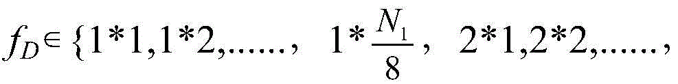
According to the above table one, the input signal frequency
Are divided into five groups: each group has the length of
By f
D The lower 10 bits of (2) represent; f (f)
D The upper 5 bits of (2) represent the labels k, k e {2 }
0 ,2
1 ,2
2 ,2
3 ,2
4 ,2
6 }. Thus, from the above tables, one skilled in the art can extend the following:
input signal frequency
Is divided into n groups, each group length
By f
D Low (S) of (C)
Bit indicates, f
D The upper n bits represent the labels k, k e {2 }, of each group of frequencies
0 ,2
1 ,2
2 ,......,2
n -a }; low and low
The value of a bit represents
In an embodiment of the present invention, the input signal frequency f
D =k×ftw, where k represents a frequency expansion coefficient,
DDS signal frequency f=f
D ×f
H_ratio The method comprises the steps of carrying out a first treatment on the surface of the Thus, in an embodiment of the present invention, the value k ε {2 for the upper H bits
0 ,2
1 ,2
2 ,......,2
n -said DDS frequency control word ∈ }>
Wherein the selection is->
The ADC sampling frequency f is based on the sampling theorem
ADC 8 times the frequency of the input signal.
Therefore, there are two methods to increase the frequency resolution of the ADC input signal, one is to decrease the ADC sampling clock; and secondly, the length of the data of the ADC input signals is increased. The digital phase demodulation method of the present invention increases the length of the data of the ADC input signal to increase the frequency resolution of the ADC input signal.
As shown in fig. 4 and 5, a further embodiment of the present invention provides a digital phase demodulation system for bioelectrical impedance measurement, the system comprising:
a signal extractor for extracting a received input signal S (n), wherein n is a sequence number and
the length of the input signal S (N) is N;
demodulation controller controlled by a given input signal frequency fAfter demodulation, the decimation factor M, the frequency control word FTW and the working clock frequency f are output DDS ;
A local oscillator signal synthesizer (DDS) for controlling the word FTW and the read clock f according to the frequency DDS To control the generation of cosine and sine signals, wherein the DDS has a sampling length of N 1 ;
The two multipliers are used for multiplying the signal Y (n) obtained after M times of extraction of the signal extractor with the cosine signal and sine signal data generated by the local oscillation signal synthesizer respectively;
two filters for filtering high frequency components of the multiplier signal according to the signal from the multiplier to output real part I and imaginary part Q of the input signal S (n);
wherein the demodulation controller includes:
a shift register I for receiving the frequency f of the input signal D Taking high H bits and outputting a high H bit value k;
a divider connected with the shift register I for dividing the high-order value k according to the output of the shift register I
Dividing factor D and extraction factor M are obtained after dividing the k value;
the frequency divider is connected with the divider and is used for obtaining a DDS working clock f according to a frequency division factor D output by the divider DDS ;
Shift register II for receiving input signal frequency f
D Take the low L bits and output the low L bit value
After shift register processing, the DDS frequency control word FTW is directly output.
In an embodiment of the present invention, the local oscillator signal synthesizer (DDS) includes:
the two phase accumulators are used for linearly accumulating the phases of the local oscillation signals according to the frequency control word FTW output by the shift register II in the demodulation controller;
two waveform memories for obtaining clock frequency f according to frequency divider
DDS To control the local oscillation signal to obtain cosine signal after processing by two phase accumulators
And sine signal->
In the embodiment of the invention, the two filters are low-pass filters, and the two waveform memories are ROM.
As further shown in FIG. 4, the workflow is that the input signal S (n) is processed by the signal extractor and then is respectively combined with local oscillation signals generated by the DDS
Is->
Multiplying and then passing through a low pass filter (LF) to obtain real I and imaginary Q signals of the input signal.
The demodulation controller is used for controlling the digital frequency f according to the input signal
D Obtaining the extraction factor M of the signal extractor, the frequency control word FTW of the DDS and the working clock f of the DDS
DDS The method comprises the steps of carrying out a first treatment on the surface of the Thereby ensuring that the frequency of the input signal is consistent with the frequency of the signal generated by the DDS. Wherein the signal extractor is implemented to extract data once every M points. Frequency of DDS signal
Wherein FTW is the frequency control word of DDS. The digital phase demodulation system of the invention adopts the method of reducing the DDS working clock f because the increase of the storage depth of the waveform memory (ROM) increases the hardware cost
DDS The DDS frequency separation rate is improved.
The foregoing is merely exemplary of the present invention, and it is not to be construed as limiting the invention to the specific embodiments and application scope of the invention, as modifications will become apparent to those of ordinary skill in the art upon review of the teachings herein.