CN101803917A - Bio-electrical impedance imaging hardware system - Google Patents
Bio-electrical impedance imaging hardware system Download PDFInfo
- Publication number
- CN101803917A CN101803917A CN 201010133501 CN201010133501A CN101803917A CN 101803917 A CN101803917 A CN 101803917A CN 201010133501 CN201010133501 CN 201010133501 CN 201010133501 A CN201010133501 A CN 201010133501A CN 101803917 A CN101803917 A CN 101803917A
- Authority
- CN
- China
- Prior art keywords
- control module
- data
- fpga
- conversion
- module
- Prior art date
- Legal status (The legal status is an assumption and is not a legal conclusion. Google has not performed a legal analysis and makes no representation as to the accuracy of the status listed.)
- Granted
Links
Images


Landscapes
- Measurement And Recording Of Electrical Phenomena And Electrical Characteristics Of The Living Body (AREA)
Abstract
Description
技术领域technical field
本发明涉及一种医疗设备,特别涉及一种生物电阻抗成像硬件系统。The invention relates to a medical device, in particular to a bioelectrical impedance imaging hardware system.
背景技术Background technique
生物电阻抗成像是一种新型的、低廉的、无损的成像技术,其基本原理为向人体注入安全的电物理量(如电流或电压),测量体表相应的电学物理量,对目标体内电阻抗分布进行重建的一种新型成像方法。在生物电阻抗成像中,成像图像的质量与电极数目密切相关,而电极数目越多所传输的数据信息量也就越大。现有的生物电阻抗成像系统数据采集和数据传输电路基本上通过模拟信号发生电路,多路选择集成电路,计数器集成电路,单片机主控芯片,串口通信电路和滤波电路等组成,其电路较复杂,模拟电路成分多,从而导致生物电阻抗成像系统功耗大,体积大,并存在抗干扰能力弱,维护升级成本高和数据采集速度低等问题。针对上述问题,虽然已有一些研究人员对生物电阻抗成像硬件系统进行了局部该进,如天津大学王化祥教授研发的基于FPGA的生物电阻抗成像系统的恒流源等,但上述问题并未得到系统解决。本发明的生物电阻抗成像硬件系统提高了电路的集成度,并增强其可扩展性和升级性,从而大大减少硬件系统的体积和功耗,节约成本,并提高了抗干扰性。Bioelectrical impedance imaging is a new, cheap, and non-destructive imaging technology. Its basic principle is to inject safe electrical physical quantities (such as current or voltage) into the human body, measure the corresponding electrical physical quantities on the body surface, and analyze the distribution of electrical impedance in the target body. A novel imaging method for reconstruction. In bioelectrical impedance imaging, the quality of imaging images is closely related to the number of electrodes, and the larger the number of electrodes, the greater the amount of data information transmitted. The existing bioelectrical impedance imaging system data acquisition and data transmission circuit is basically composed of an analog signal generation circuit, a multi-channel selection integrated circuit, a counter integrated circuit, a single-chip microcomputer main control chip, a serial communication circuit and a filter circuit, etc., and the circuit is relatively complicated. , There are many analog circuit components, resulting in high power consumption, large volume, weak anti-interference ability, high maintenance and upgrade costs, and low data acquisition speed of the bioelectrical impedance imaging system. In view of the above problems, although some researchers have made local improvements to the bioelectrical impedance imaging hardware system, such as the constant current source of the FPGA-based bioelectrical impedance imaging system developed by Professor Wang Huaxiang of Tianjin University, the above problems have not been solved. System solved. The biological electrical impedance imaging hardware system of the present invention improves the integration degree of the circuit, and enhances its scalability and upgradeability, thereby greatly reducing the volume and power consumption of the hardware system, saving costs, and improving the anti-interference performance.
发明内容Contents of the invention
本发明所要解决的技术问题是,针对现有技术中的缺陷,设计一种利用现场可编程门阵列技术(Field Programmable Gate Array,FPGA)和USB通讯技术实现体积小,功耗低,电路结构简单,易于维护升级的生物电阻抗成像硬件系统。The technical problem to be solved by the present invention is, aiming at the defects in the prior art, design a kind of utilizing Field Programmable Gate Array technology (Field Programmable Gate Array, FPGA) and USB communication technology to realize volume is small, power consumption is low, and circuit structure is simple , easy to maintain and upgrade bioelectrical impedance imaging hardware system.
本发明采用的总体技术方案是:The general technical scheme that the present invention adopts is:
一种生物电阻抗成像硬件系统,包括如下几个部分:A bioelectrical impedance imaging hardware system includes the following parts:
上位机,用于接收采集的电压数据,重建并显示图像;The upper computer is used to receive the collected voltage data, reconstruct and display the image;
USB接口芯片,用于接收FPGA控制器的控制信号和数据,完成USB传输功能;The USB interface chip is used to receive control signals and data from the FPGA controller to complete the USB transmission function;
D/A转换、滤波和压流转换电路,包括D/A转换器件,带通滤波电路和Howland电路,用于将FPGA控制器输出的数据转换成可用于注入被测对象的恒定电流;D/A conversion, filtering and voltage-current conversion circuits, including D/A conversion devices, band-pass filter circuits and Howland circuits, are used to convert the data output by the FPGA controller into a constant current that can be injected into the measured object;
多路开关,用于接收FPGA控制器输出的控制信号从而确定被测对象上被选通的电极;The multi-way switch is used to receive the control signal output by the FPGA controller so as to determine the gated electrodes on the measured object;
放大、滤波和A/D转换电路,包括放大电路、带通滤波电路和A/D转换电路,用于将测量出的电压信号进行预处理并对预处理过的信号进行模数转换,最终将转换后的数据输入FPGA控制器;Amplification, filtering and A/D conversion circuits, including amplification circuits, band-pass filter circuits and A/D conversion circuits, are used to preprocess the measured voltage signals and perform analog-to-digital conversion on the preprocessed signals, and finally convert The converted data is input to the FPGA controller;
FPGA控制器,用于控制上述各部分协调工作。The FPGA controller is used to control the coordinated work of the above-mentioned parts.
所述的FPGA控制器控制过程具体包括,通过控制USB接口芯片接收上位机传来的命令并传递成像数据给上位机,控制多路开关确定选通电极,接收放大、滤波和A/D转换电路输入的数字电压信号并对电压信号进行数字相敏解调,控制D/A转换、滤波和压流转换电路输出恒定电流。The control process of the FPGA controller specifically includes, receiving commands from the host computer by controlling the USB interface chip and transmitting imaging data to the host computer, controlling the multi-way switch to determine the gate electrode, receiving amplification, filtering and A/D conversion circuits The input digital voltage signal is digitally phase-sensitively demodulated, and the D/A conversion, filtering and voltage-current conversion circuits are controlled to output a constant current.
所述的FPGA控制器包括恒流源控制模块,多路开关选择控制模块,A/D转换采样控制模块,数字相敏解调模块,USB传输控制模块和总控制模块,其中,The FPGA controller includes a constant current source control module, a multi-way switch selection control module, an A/D conversion sampling control module, a digital phase-sensitive demodulation module, a USB transmission control module and a total control module, wherein,
所述的恒流源控制模块用于输出可转化为注入被测对象的恒定电流的数据;The constant current source control module is used to output data that can be converted into a constant current injected into the measured object;
所述的多路开关选择控制模块用于控制所述的多路开关以选择不同的注电路测电压模式;The multi-way switch selection control module is used to control the multi-way switch to select different injection circuit voltage measurement modes;
所述的A/D转换采样控制模块用于控制所述的放大、滤波和A/D转换电路的A/D转换频率并接收A/D转换电路转换出来的数据;The A/D conversion sampling control module is used to control the A/D conversion frequency of the amplification, filtering and A/D conversion circuit and receive the data converted by the A/D conversion circuit;
所述的数字相敏解调模块通过数字相敏解调的方法,把上述转换出来的数据与FPGA内部正弦和余弦表进行计算,解调出包含实部与虚部的数字信号;The digital phase-sensitive demodulation module calculates the above-mentioned converted data and FPGA internal sine and cosine tables by means of digital phase-sensitive demodulation, and demodulates digital signals comprising real and imaginary parts;
所述的USB传输控制模块控制USB接口芯片工作在的批量传输模式,完成USB传输功能;The USB transmission control module controls the batch transmission mode in which the USB interface chip works, and completes the USB transmission function;
所述的总控制模块控制各个模块的工作,通过分发控制字决定以上模块的工作状态,并完成各模块之间数据缓冲和传输的功能。The general control module controls the work of each module, determines the working status of the above modules by distributing control words, and completes the functions of data buffering and transmission between modules.
所述的FPGA控制器各模块均在FPGA中采用硬件描述语言编程实现。Each module of the FPGA controller is implemented in the FPGA using hardware description language programming.
所述的恒流源控制模块是通过FPGA将其内部ROM中的正弦表数据输出给所述的D/A转换、滤波和压流转换电路。The constant current source control module outputs the sine table data in its internal ROM to the D/A conversion, filtering and voltage-current conversion circuits through FPGA.
所述的多路开关选择控制模块的功能通过在FPGA内编写状态机来实现。The function of the multi-way switch selection control module is realized by writing a state machine in FPGA.
所述的A/D转换采样控制模块产生的采样时钟由FPGA内部编写的定时器完成,接收A/D转换的数据的功能由FPGA内部编写的双端口ROM实现。The sampling clock generated by the A/D conversion sampling control module is completed by a timer programmed inside the FPGA, and the function of receiving A/D converted data is realized by a dual-port ROM written inside the FPGA.
所述的总控制模块由硬件描述语言Verlog HDL编写状态机来实现,具体为:总控制模块分为五个状态,分别为等待命令,接收命令,分发控制字,接收相敏解调数据和传输相敏解调数据,所述等待命令状态为不断轮询USB传输控制模块是否有数据输入;所述接收命令状态为接收USB传输控制模块传来的命令数据并分析这些数据完整性和正确性,即判断各命令控制字的值是否在其各自的值域范围内;所述分发控制字状态为将所收到的各命令控制字分别传输到相应的模块;所述接收相敏解调数据状态为检查数字相敏解调模块的工作是否完成,如果相敏解调完成就接收数字相敏解调模块传入的数据,反之等待;所述传输相敏解调数据状态为将所收到的相敏解调数据送入USB传输控制模块。Described total control module is realized by state machine written by hardware description language Verlog HDL, specifically: total control module is divided into five states, is respectively waiting for command, receiving command, distributing control word, receiving phase-sensitive demodulation data and transmission Phase-sensitive demodulation data, the waiting command state is continuously polling whether the USB transmission control module has data input; the receiving command state is receiving the command data from the USB transmission control module and analyzing the integrity and correctness of these data, That is to judge whether the value of each command control word is within its respective value range; the state of the distribution control word is to transmit each received command control word to the corresponding module respectively; the state of receiving phase-sensitive demodulation data To check whether the work of the digital phase-sensitive demodulation module is completed, if the phase-sensitive demodulation is completed, the incoming data of the digital phase-sensitive demodulation module is received, otherwise wait; the state of the transmitted phase-sensitive demodulation data is the received The phase-sensitive demodulation data is sent to the USB transmission control module.
采用FPGA技术设计的生物电阻抗成像硬件系统,提高了电路的集成度,并增强其可扩展性和升级性,从而大大减少硬件系统的体积和功耗,节约成本,提高了抗干扰性,在信息采集和医学电子仪器上有着广泛的应用前景。The bioelectrical impedance imaging hardware system designed with FPGA technology improves the integration of the circuit, and enhances its scalability and upgradeability, thereby greatly reducing the size and power consumption of the hardware system, saving costs, and improving anti-interference performance. It has broad application prospects in information collection and medical electronic instruments.
附图说明Description of drawings
图1为生物电阻抗成像系统整体框图;Fig. 1 is the overall block diagram of the bioelectrical impedance imaging system;
图2为FPGA控制器的模块图;Fig. 2 is the block diagram of FPGA controller;
图3为利用直接数字频率合成技术(DDS)产生激励恒流源的原理图;Fig. 3 is the principle diagram that utilizes direct digital frequency synthesis technology (DDS) to generate the excitation constant current source;
图4为数字相敏解调模块原理图。Figure 4 is a schematic diagram of the digital phase-sensitive demodulation module.
具体实施方式Detailed ways
以下结合附图和实施例对本发明做进一步的详细描述。The present invention will be described in further detail below in conjunction with the accompanying drawings and embodiments.
本发明基于FPGA技术设计了一种生物电阻抗成像硬件系统,该系统包括如下几部分:The present invention has designed a kind of bioelectrical impedance imaging hardware system based on FPGA technology, and this system comprises following several parts:
上位机1,此部分由工控机或PC机组成,用来接收采集的电压数据,采用常规的软件算法(如等位线逆投影)来重建并显示图像;Host computer 1, this part is composed of industrial computer or PC, which is used to receive the collected voltage data, and use conventional software algorithms (such as equipotential line back projection) to reconstruct and display images;
USB接口芯片2,此部分由USB接口芯片组成,接收FPGA控制器的控制信号和数据,完成USB传输功能;USB interface chip 2, this part is composed of USB interface chip, receives the control signal and data of the FPGA controller, and completes the USB transmission function;
D/A转换、滤波和压流转换电路3,此部分由D/A转换器件,带通滤波电路和Howland电路组成,将FPGA控制器输出的数据转换成可用于注入被测对象5的恒定电流;D/A conversion, filtering and voltage-current conversion circuit 3, this part is composed of D/A conversion device, band-pass filter circuit and Howland circuit, converts the data output by the FPGA controller into a constant current that can be injected into the measured object 5 ;
多路开关4和6,此部分由多路开关芯片组成,接收FPGA控制器输出的控制信号从而决定那个电极被选通;Multi-way switches 4 and 6, this part is composed of multi-way switch chips, which receive the control signal output by the FPGA controller to determine which electrode is gated;
放大,滤波和A/D转换电路7部分,此部分由放大电路,带通滤波电路和A/D转换电路组成,将测量的电压信号进行预处理并由FPGA控制器控制A/D转换器件对预处理过的信号进行模数转换,最终将转换后的数据输入FPGA控制器。There are 7 parts of amplification, filtering and A/D conversion circuit. This part is composed of amplification circuit, band-pass filter circuit and A/D conversion circuit. The measured voltage signal is preprocessed and the A/D conversion device is controlled by the FPGA controller. The preprocessed signal is converted from analog to digital, and finally the converted data is input to the FPGA controller.
FPGA控制器部分,此部分由恒流源控制模块,多路开关选择控制模块,A/D转换采样控制模块,数字相敏解调模块,USB传输控制模块,总控制模块组成。FPGA controller part, this part is composed of constant current source control module, multi-way switch selection control module, A/D conversion sampling control module, digital phase-sensitive demodulation module, USB transmission control module, and general control module.
如图2,所述FPGA控制器的所有模块都在FPGA内完成,各模块结构和功能详述如下:As shown in Figure 2, all modules of the FPGA controller are completed in the FPGA, and the structure and functions of each module are described in detail as follows:
1,恒流源控制模块1. Constant current source control module
本模块采用直接数字频率合成(DDS)技术,利用Matlab软件产生正弦表数据,并把这些数据存入FPGA芯片内部的只读ROM中。在利用FPGA内部的锁相环电路(PLL)输出稳定时钟,这个稳定的时钟和累加器所产生的地址信号将一起驱动FPGA内部只读ROM,把ROM中的正弦表数据输出到D/A转换,滤波和压流转换电路3,在此过程中累加器的初始值由输入相位控制字决定,累加器的步长由输入频率控制字决定,相位控制字和频率控制字由总控制模块分发。本模块输出的数字信号经过D/A转换、滤波、放大隔离,最终还原成由相位控制字和频率控制字决定的正弦电压信号。正弦的电压信号再通过改进的Howland电路转化成电流信号以便注入被测对象5。采用DDS技术的产生激励源原理图如图3所示。This module uses direct digital frequency synthesis (DDS) technology, uses Matlab software to generate sine table data, and stores these data in the read-only ROM inside the FPGA chip. Using the phase-locked loop circuit (PLL) inside the FPGA to output a stable clock, this stable clock and the address signal generated by the accumulator will drive the read-only ROM inside the FPGA together, and output the sine table data in the ROM to the D/A conversion , filtering and pressure-current conversion circuit 3, during this process the initial value of the accumulator is determined by the input phase control word, the step size of the accumulator is determined by the input frequency control word, and the phase control word and frequency control word are distributed by the general control module. The digital signal output by this module undergoes D/A conversion, filtering, amplification and isolation, and finally restores to a sinusoidal voltage signal determined by the phase control word and frequency control word. The sinusoidal voltage signal is converted into a current signal through the improved Howland circuit so as to be injected into the measured object 5 . The schematic diagram of the excitation source produced by DDS technology is shown in Figure 3.
2,多路开关选择模块2. Multi-way switch selection module
多路开关选择模块是在FPGA内编写状态机来实现,此模块产生A0,A1,A2,A3分别为四位二进制数地址信号,其中,A0和A1用于选择加载激励电流的电极,A2,A3用于选择测量电压的电极,通过接收不同的模式控制字(MODE)可以选择A0,A1,A2,A3的变化模式,从而产生不同的电压测量模式,如相邻注电流相邻测电压模式,相邻注电流相对测电压模式,相对注电流相邻测电压模式等等,可实现灵活多变的测量,以上的不同测量模式可以用硬件描述语言编写出不同的状态机来完成,从而可实现自定义的测量模式,为后期电阻抗成像技术的发展提供了一个很好的硬件平台。The multi-way switch selection module is implemented by writing a state machine in the FPGA. This module generates A0, A1, A2, and A3 respectively as four-digit binary address signals. Among them, A0 and A1 are used to select the electrodes that load the excitation current, A2, A3 is used to select the electrode for measuring voltage. By receiving different mode control words (MODE), the change mode of A0, A1, A2, and A3 can be selected, so as to generate different voltage measurement modes, such as adjacent injection current adjacent voltage measurement mode , Adjacent current injection relative voltage measurement mode, relative current injection adjacent voltage measurement mode, etc., can realize flexible and changeable measurement. The above different measurement modes can be completed by writing different state machines in hardware description language, so that The realization of custom measurement mode provides a good hardware platform for the development of electrical impedance imaging technology in the later stage.
此模块产生的地址信号控制多路开关4和多路开关6两部分,即按所需激励方式产生A0和A1地址信号控制多路开关4部分将激励电流加载到要求的16个激励电极中的一对电极上,按所需的测量方式产生A2和A3地址信号控制多路开关6部分将16个测量电极中的一对电极上的电压加载到放大,滤波和A/D转换电路7部分的输入端。The address signal generated by this module controls the two parts of multi-way switch 4 and multi-way switch 6, that is, generates A0 and A1 address signals according to the required excitation mode to control the multi-way switch 4 part to load the excitation current to the required 16 excitation electrodes. On a pair of electrodes, A2 and A3 address signals are generated according to the required measurement method to control the multi-way switch. Part 6 loads the voltage on a pair of electrodes among the 16 measuring electrodes to the amplification, filtering and A/D conversion circuit in part 7. input.
本实施实例中多路开关部分采用的是美信公司生产的CMOS十六通道模拟多路开关MAX306(其导通电阻最大为100Ω,通道间的电阻匹配误差最大为5Ω,开关时间小于400ns)The multi-channel switch part in this implementation example adopts the CMOS sixteen-channel analog multi-channel switch MAX306 produced by Maxim (the maximum on-resistance is 100Ω, the maximum resistance matching error between channels is 5Ω, and the switching time is less than 400ns)
3,A/D转换采样控制模块3. A/D conversion sampling control module
A/D转换采样控制模块由硬件描述语言编程实现,完成采样时钟的输出和A/D转换数据的接收并传入数字相敏解调模块,采样的时钟由FPGA内部编写的定时器完成,定时器的周期由总控制模块分发的采样频率控制字决定,接收A/D转换的数据并传入数字相敏解调模块的功能由FPGA内部编写的双端口ROM实现。本模块用来控制放大,滤波和A/D转换电路7部分的A/D转换频率并接收A/D转换出来的数据。The A/D conversion sampling control module is implemented by hardware description language programming, completes the output of the sampling clock and the reception of the A/D conversion data and transmits it to the digital phase-sensitive demodulation module. The sampling clock is completed by the timer programmed inside the FPGA. The cycle of the device is determined by the sampling frequency control word distributed by the general control module, and the function of receiving A/D converted data and passing it into the digital phase-sensitive demodulation module is realized by the dual-port ROM written inside the FPGA. This module is used to control the A/D conversion frequency of the 7 parts of the amplification, filtering and A/D conversion circuit and receive the A/D converted data.
4,数字相敏解调模块4. Digital phase-sensitive demodulation module
数字相敏解调模块由硬件描述语言编程完成,本实施例为在正弦波周期电压信号的一个周期内使用A/D转换器件采样250次,生成250个数据。这些数据再和FPGA内ROM中分别存放两张表做计算,一张为正弦表,一张为余弦表,在一个周期内计算虚部分量I和实部分量Q的常规公式如下:The digital phase-sensitive demodulation module is programmed by the hardware description language. In this embodiment, the A/D conversion device is used to sample 250 times in one cycle of the sine wave periodic voltage signal, and 250 data are generated. These data are then stored in two tables in the ROM of the FPGA for calculation, one is a sine table and the other is a cosine table. The general formula for calculating the imaginary component I and the real component Q in one cycle is as follows:
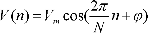


在FPGA内实现的原理图如图4,当FPGA解调出I和Q值后,将其值送入总控制模块,总控制模块再将数据传给USB传输控制模块,USB传输控制模块控制USB接口芯片将相敏解调出来的数据传入上位机。在上位机中可用如下公式计算出电压信号的振幅和相位。The schematic diagram implemented in the FPGA is shown in Figure 4. After the FPGA demodulates the I and Q values, the values are sent to the general control module, which then transmits the data to the USB transmission control module, and the USB transmission control module controls the USB The interface chip transmits the phase-sensitive demodulated data to the host computer. The following formula can be used to calculate the amplitude and phase of the voltage signal in the host computer.

其中V(n)为经A/D转换器件采样的数据,q(n)和r(n)分别为正弦表和余弦表。n为自然数,N在本实施例的系统中取250,Vm为振幅,
5,USB传输控制模块5. USB transmission control module
USB传输控制模块所要控制的接口芯片是CYPRESS公司生产的EZ-USB FX2(即CY7C68013)。此芯片集成了USB通信控制引擎(SIE)和改进的8051内核于一体,能完成三种模式的传输,USB的低速传输1.5Mbps,全速传输12Mbps和高速传输480Mbps。USB传输控制模块产生少量控制信号(即读信号SLRD,写信号SLWD,使能信号SLOE,写满信号FLAGB,端口选择信号FADDR0和FADDR1)和数据总线便可进行高速USB传输。USB的控制信号由USB传输控制模块发出,此模块在FPGA内由硬件描述语言编写状态机来实现。The interface chip to be controlled by the USB transmission control module is EZ-USB FX2 (namely CY7C68013) produced by CYPRESS. This chip integrates the USB communication control engine (SIE) and the improved 8051 core, and can complete three modes of transmission, USB low-speed transmission of 1.5Mbps, full-speed transmission of 12Mbps and high-speed transmission of 480Mbps. The USB transmission control module generates a small amount of control signals (read signal SLRD, write signal SLWD, enable signal SLOE, write full signal FLAGB, port selection signals FADDR0 and FADDR1) and data bus to perform high-speed USB transmission. The USB control signal is issued by the USB transmission control module, which is implemented by writing a state machine in a hardware description language in the FPGA.
USB传输控制模块控制的接口芯片的固件程序是在CPYPRESS公司提供的固件框架程序下编程,只需修改初始化函数TD_Init()和TD_POLL(),方便简单,本系统中通过设定接口芯片寄存器的值使得USB的驱动频率为48MHz,从FIFO模式,异步读写,不使用IFCLK引脚。The firmware program of the interface chip controlled by the USB transmission control module is programmed under the firmware framework program provided by CPYPRESS, and only needs to modify the initialization functions TD_Init() and TD_POLL(), which is convenient and simple. In this system, the value of the interface chip register is set. The driving frequency of the USB is 48MHz, from the FIFO mode, asynchronously read and write, and the IFCLK pin is not used.
为完成USB通讯功能,上位机的USB的驱动程序直接使用CYPRESS公司提供的驱动程序ezusb.sys,应用程序则调用其API函数,主要有CreatFile()和DeviceIoControl()。CreatFile()的功能是取得设备句柄,DeviceIoControl()的功能是向设备驱动程序发送请求,应用程序的主要功能是开启或关闭USB设备,设定传输参数,启动或停止采集传输等。In order to complete the USB communication function, the USB driver of the upper computer directly uses the driver ezusb.sys provided by CYPRESS, and the application program calls its API functions, mainly CreatFile() and DeviceIoControl(). The function of CreatFile() is to obtain the device handle, and the function of DeviceIoControl() is to send a request to the device driver. The main function of the application is to turn on or off the USB device, set the transmission parameters, start or stop the acquisition and transmission, etc.
6,总控制模块6. General control module
总控制模块是整个电路的核心部分,它是一个功能强大的处理系统,由硬件描述语言Verlog HDL编写状态机来实现,总控制模块分为五个状态,分别为等待命令,接收命令,分发控制字,接收相敏解调数据,传输相敏解调数据。等待命令状态为不断轮询USB传输控制模块是否有数据输入,接收命令状态为接收USB传输控制模块传来的命令数据并分析这些数据完整性和正确性(判断各命令控制字的值是否在其各自的值域范围内),分发控制字状态为将所收到的各命令控制字分别传输到相应的模块。接收相敏解调数据状态为检查数字相敏解调模块的工作是否完成,如果相敏解调完成就接收数字相敏解调模块传入的数据,反之等待。传输相敏解调数据状态为将所收到的相敏解调数据送入USB传输控制模块,由USB传输控制模块负责将相敏解调的数据通过USB接口芯片传给上位机。总控制模块主要作用是协调和控制各个模块的工作,用于使能各个模块,接受并分发送控制字,数据缓冲和传输等。The total control module is the core part of the entire circuit. It is a powerful processing system, which is realized by writing a state machine in the hardware description language Verlog HDL. The total control module is divided into five states, which are respectively waiting for commands, receiving commands, and distributing control Word, receive phase-sensitive demodulation data, transmit phase-sensitive demodulation data. The waiting command state is to constantly poll whether the USB transmission control module has data input, and the receiving command state is to receive the command data sent by the USB transmission control module and analyze the integrity and correctness of these data (judging whether the value of each command control word is within its within the range of their respective value ranges), the status of the distribution control word is to transmit the received command control words to the corresponding modules respectively. The status of receiving phase-sensitive demodulation data is to check whether the work of the digital phase-sensitive demodulation module is completed. If the phase-sensitive demodulation is completed, it will receive the data from the digital phase-sensitive demodulation module, otherwise wait. The state of transmitting phase-sensitive demodulated data is to send the received phase-sensitive demodulated data to the USB transmission control module, and the USB transmission control module is responsible for transmitting the phase-sensitive demodulated data to the host computer through the USB interface chip. The main function of the general control module is to coordinate and control the work of each module, to enable each module, to receive and distribute control words, to buffer and transmit data, etc.
系统上电后,按如下流程工作:After the system is powered on, it works as follows:
(1)系统中FPGA芯片经过上电复位,配置后进入用户模式,在用户模式中,FPGA中的USB传输控制模块先初始化,控制指定传输的端点,并检查端点FIFO的空(empty)信号,等待上位机传来的命令。(1) The FPGA chip in the system enters the user mode after power-on reset and configuration. In the user mode, the USB transmission control module in the FPGA is initialized first, controls the specified transmission endpoint, and checks the empty (empty) signal of the endpoint FIFO. Wait for the command from the host computer.
(2)如检测到有命令传输,USB传输控制模块控制USB接口芯片进行USB传输,将命令数据传入总控制模块,总控制模块接受命令并判断其是否有效,如果命令控制字无效,总控制模块回到等待命令状态不进行下一步动作。(2) If a command transmission is detected, the USB transmission control module controls the USB interface chip to perform USB transmission, and transmits the command data to the total control module, which accepts the command and judges whether it is valid. If the command control word is invalid, the total control The module returns to the state of waiting for commands without further action.
(3)如果命令有效,总控制模块将频率控制字,相位控制字,模式选者控制字,数字相敏解调采样率控制字分别传送给各自模块,各模块按照控制字所决定的工作模式执行一个测量周期。被测对象5由周围一圈均与摆放16个电极(可扩展)的圆柱体模型组成,圆柱体内布置有不同阻抗值的物质,可用于生物电阻抗成像硬件系统的测量;(3) If the command is valid, the master control module will transmit the frequency control word, phase control word, mode selector control word, and digital phase-sensitive demodulation sampling rate control word to their respective modules, and each module will follow the working mode determined by the control word Execute a measurement cycle. The measured object 5 is composed of a cylinder model with 16 electrodes (expandable) placed in a circle around it, and substances with different impedance values are arranged in the cylinder, which can be used for the measurement of the bioelectrical impedance imaging hardware system;
测量周期的一个实例如下:如本系统使用一种相邻电极注电流相邻电极测电压的方式,共16个电极(可扩展),先用1-2电极对注电流,然后分别测3-4电极对,4-5电极对一直到15-16电极对共13对电极的电压信号,再换2-3电极对注电流,测4-5电极对,5-6电极对一直到16-1电极对共13对电极的电压信号,如此循环一圈共有13(对)*16(次)共208个电压信号,这些电压信号经过放大,滤波和A/D转换电路7部分后输入A/D转换采样控制模块,最后将数据送入数字相敏解调模块,完成一个测量周期。An example of the measurement cycle is as follows: If this system uses a method of injecting current into adjacent electrodes and measuring voltage on adjacent electrodes, there are 16 electrodes in total (expandable), first use 1-2 electrodes to inject current, and then measure 3- 4 electrode pairs, 4-5 electrode pairs until 15-16 electrode pairs, a total of 13 pairs of electrode voltage signals, and then change 2-3 electrode pairs to inject current, measure 4-5 electrode pairs, 5-6 electrode pairs until 16- 1 electrode pair, a total of 13 pairs of electrode voltage signals, so a total of 13 (pairs) * 16 (times) a total of 208 voltage signals, these voltage signals are amplified, filtered and A/D conversion circuit 7 parts and then input into A/D D converts the sampling control module, and finally sends the data to the digital phase-sensitive demodulation module to complete a measurement cycle.
(4)数字相敏解调模块对接收的数据进行解调。(4) The digital phase-sensitive demodulation module demodulates the received data.
(5)总控制模块接收数字相敏解调模块解调出的数据再将这些数据送入USB传输控制模块,然后USB传输控制模块控制USB接口芯片将数据传给上位机。(5) The general control module receives the data demodulated by the digital phase-sensitive demodulation module and sends the data to the USB transmission control module, and then the USB transmission control module controls the USB interface chip to transmit the data to the host computer.
(6)完成一次测量采集后,重复(2)-(4)步骤进行下一次采集。(6) After completing one measurement acquisition, repeat steps (2)-(4) for the next acquisition.
(7)在上位机中,上位机接收USB接口传来的数据,利用等位线逆投影算法或一步牛顿法等,重建并显示目标图像。(7) In the host computer, the host computer receives the data from the USB interface, and uses the equipotential line back-projection algorithm or one-step Newton method to reconstruct and display the target image.
该发明的硬件描述语言编程载体可选用Altera的Cylone系列芯片,该系统大部分内容都可由FGPA集成电路完成,只需少量芯片外部配合,如A/D,D/A,COMS多路开关,USB接口芯片等,这样能提高硬件系统的集成度,对所测数据进行适当的前端处理,减小其体积,减小功耗,节约成本和提高可维护性并提高了数据的传输速度,可升级性好。The hardware description language programming carrier of this invention can be used Altera's Cylone series chips, most of the content of the system can be completed by FGPA integrated circuits, only a small amount of external cooperation with chips, such as A/D, D/A, COMS multi-way switch, USB Interface chips, etc., which can improve the integration of the hardware system, perform proper front-end processing on the measured data, reduce its size, reduce power consumption, save costs, improve maintainability and increase data transmission speed, and can be upgraded Good sex.
本发明可用其他的不违背本发明的精神或主要特征的具体形式来概述,本发明的上述实施方案都只能认为是对本发明的说明而不能限制本发明,在与本发明的权利要求书相当的含义和范围内的任何改变,都应认为是包括在权利要求书的范围内。因此,本发明以权利要求书的保护范围为准。The present invention can be summarized by other specific forms that do not deviate from the spirit or main characteristics of the present invention. The above-mentioned embodiments of the present invention can only be considered as illustrations of the present invention and cannot limit the present invention. They are equivalent to the claims of the present invention. Any change within the meaning and scope should be considered to be included in the scope of the claims. Therefore, the present invention is based on the protection scope of the claims.
Claims (8)
Priority Applications (1)
| Application Number | Priority Date | Filing Date | Title |
|---|---|---|---|
| CN2010101335019A CN101803917B (en) | 2010-03-29 | 2010-03-29 | Bio-electrical impedance imaging hardware system |
Applications Claiming Priority (1)
| Application Number | Priority Date | Filing Date | Title |
|---|---|---|---|
| CN2010101335019A CN101803917B (en) | 2010-03-29 | 2010-03-29 | Bio-electrical impedance imaging hardware system |
Publications (2)
| Publication Number | Publication Date |
|---|---|
| CN101803917A true CN101803917A (en) | 2010-08-18 |
| CN101803917B CN101803917B (en) | 2012-01-25 |
Family
ID=42605997
Family Applications (1)
| Application Number | Title | Priority Date | Filing Date |
|---|---|---|---|
| CN2010101335019A Expired - Fee Related CN101803917B (en) | 2010-03-29 | 2010-03-29 | Bio-electrical impedance imaging hardware system |
Country Status (1)
| Country | Link |
|---|---|
| CN (1) | CN101803917B (en) |
Cited By (16)
| Publication number | Priority date | Publication date | Assignee | Title |
|---|---|---|---|---|
| CN102355264A (en) * | 2011-07-22 | 2012-02-15 | 中电普瑞科技有限公司 | Analogue-to-digital conversion circuit for portable electric energy monitoring device |
| CN103617140A (en) * | 2013-11-25 | 2014-03-05 | 北京航空航天大学 | Electroneurographic signal compressed sensing processing verification system and construction method thereof |
| CN103610463A (en) * | 2013-11-28 | 2014-03-05 | 中山大学 | Urine electrical conductivity dynamic monitoring device and method |
| CN103690166A (en) * | 2013-12-16 | 2014-04-02 | 天津科技大学 | PXI-bus-based respiration process three-dimensional electrical impedance imaging system and imaging method thereof |
| CN104483554A (en) * | 2014-12-31 | 2015-04-01 | 思澜科技(成都)有限公司 | Digital phase demodulating method and system for bioelectricity impedance measurement |
| CN104939825A (en) * | 2015-06-24 | 2015-09-30 | 中国医学科学院生物医学工程研究所 | Wearable electrical impedance tomography gastric motility information extracting device and method |
| CN105748072A (en) * | 2016-02-01 | 2016-07-13 | 上海交通大学 | High-precision multi-frequency distributed medical impedance imaging measuring system and method |
| CN108228528A (en) * | 2017-12-28 | 2018-06-29 | 苏州联视泰电子信息技术有限公司 | A kind of miniaturization digiverter and application based on FPGA |
| CN108387264A (en) * | 2018-01-30 | 2018-08-10 | 华南理工大学 | A kind of sensor device for face parameter detection |
| CN109284243A (en) * | 2018-11-21 | 2019-01-29 | 深圳开立生物医疗科技股份有限公司 | USB-based FPGA communication control device and method |
| CN109363674A (en) * | 2018-08-22 | 2019-02-22 | 西安电子科技大学 | A bioimpedance measurement system |
| CN110123320A (en) * | 2019-05-13 | 2019-08-16 | 南京航空航天大学 | A kind of portable frequency sweep impedance bioelectrical measurement system and its measurement method |
| CN110279416A (en) * | 2019-05-20 | 2019-09-27 | 南京航空航天大学 | A FPGA-based portable electrical impedance imaging system and its working method |
| CN111134674A (en) * | 2018-11-09 | 2020-05-12 | 上海交通大学 | Bioelectrical impedance tomography system based on frequency division multiplexing data compression technology |
| CN114415553A (en) * | 2021-12-07 | 2022-04-29 | 西安交通大学 | Scanning driving system and method of photoelectric device |
| CN116509368A (en) * | 2023-03-02 | 2023-08-01 | 南京航空航天大学 | Bimodal coupling detection system, method and storage medium based on electrical impedance and ultrasound |
Citations (2)
| Publication number | Priority date | Publication date | Assignee | Title |
|---|---|---|---|---|
| CN101194833A (en) * | 2006-12-08 | 2008-06-11 | 南京东影生物医学影像技术有限责任公司 | Electrical impedance galactophore scanning diagnostic device |
| CN101466303A (en) * | 2006-04-13 | 2009-06-24 | 德蒙特福特大学 | Apparatus and method for electrical impedance imaging |
-
2010
- 2010-03-29 CN CN2010101335019A patent/CN101803917B/en not_active Expired - Fee Related
Patent Citations (2)
| Publication number | Priority date | Publication date | Assignee | Title |
|---|---|---|---|---|
| CN101466303A (en) * | 2006-04-13 | 2009-06-24 | 德蒙特福特大学 | Apparatus and method for electrical impedance imaging |
| CN101194833A (en) * | 2006-12-08 | 2008-06-11 | 南京东影生物医学影像技术有限责任公司 | Electrical impedance galactophore scanning diagnostic device |
Non-Patent Citations (3)
| Title |
|---|
| 《中国优秀硕士学位论文全文数据库信息科技辑》 20090615 郭珂 电阻抗成像快速采集系统的研究 , 第6期 2 * |
| 《电子测量与仪器学报》 20060831 曲志刚,等 数字化生物电阻抗成像系统 10-14 第20卷, 第4期 2 * |
| 《电子测量技术》 20061231 问雪宁,等 用于EIT数据采集系统的USB通讯模块 第29卷, 第6期 2 * |
Cited By (25)
| Publication number | Priority date | Publication date | Assignee | Title |
|---|---|---|---|---|
| CN102355264A (en) * | 2011-07-22 | 2012-02-15 | 中电普瑞科技有限公司 | Analogue-to-digital conversion circuit for portable electric energy monitoring device |
| CN102355264B (en) * | 2011-07-22 | 2016-01-20 | 中电普瑞科技有限公司 | A kind of analog to digital conversion circuit for portable electric energy monitoring device |
| CN103617140A (en) * | 2013-11-25 | 2014-03-05 | 北京航空航天大学 | Electroneurographic signal compressed sensing processing verification system and construction method thereof |
| CN103617140B (en) * | 2013-11-25 | 2017-02-15 | 北京航空航天大学 | Electroneurographic signal compressed sensing processing verification system and construction method thereof |
| CN103610463B (en) * | 2013-11-28 | 2015-12-02 | 中山大学 | A kind of urine electrical conductivity dynamic monitor and method |
| CN103610463A (en) * | 2013-11-28 | 2014-03-05 | 中山大学 | Urine electrical conductivity dynamic monitoring device and method |
| CN103690166A (en) * | 2013-12-16 | 2014-04-02 | 天津科技大学 | PXI-bus-based respiration process three-dimensional electrical impedance imaging system and imaging method thereof |
| CN103690166B (en) * | 2013-12-16 | 2016-06-08 | 天津科技大学 | A kind of anti-imaging system of respiratory three-dimensional resistance based on PXI bus and formation method thereof |
| CN104483554A (en) * | 2014-12-31 | 2015-04-01 | 思澜科技(成都)有限公司 | Digital phase demodulating method and system for bioelectricity impedance measurement |
| CN104483554B (en) * | 2014-12-31 | 2023-07-04 | 思澜科技(成都)有限公司 | Digital phase demodulation method and system for bioelectrical impedance measurement |
| CN104939825A (en) * | 2015-06-24 | 2015-09-30 | 中国医学科学院生物医学工程研究所 | Wearable electrical impedance tomography gastric motility information extracting device and method |
| CN105748072A (en) * | 2016-02-01 | 2016-07-13 | 上海交通大学 | High-precision multi-frequency distributed medical impedance imaging measuring system and method |
| CN105748072B (en) * | 2016-02-01 | 2019-01-18 | 上海交通大学 | A kind of distributed medical electrical impedance imaging measuring system of high-precision multi-frequency and method |
| CN108228528A (en) * | 2017-12-28 | 2018-06-29 | 苏州联视泰电子信息技术有限公司 | A kind of miniaturization digiverter and application based on FPGA |
| CN108387264A (en) * | 2018-01-30 | 2018-08-10 | 华南理工大学 | A kind of sensor device for face parameter detection |
| CN109363674A (en) * | 2018-08-22 | 2019-02-22 | 西安电子科技大学 | A bioimpedance measurement system |
| CN109363674B (en) * | 2018-08-22 | 2020-07-17 | 西安电子科技大学 | A bioimpedance measurement system |
| CN111134674A (en) * | 2018-11-09 | 2020-05-12 | 上海交通大学 | Bioelectrical impedance tomography system based on frequency division multiplexing data compression technology |
| CN111134674B (en) * | 2018-11-09 | 2021-10-08 | 上海交通大学 | Bioelectrical impedance tomography system based on frequency division multiplexing data compression technology |
| CN109284243A (en) * | 2018-11-21 | 2019-01-29 | 深圳开立生物医疗科技股份有限公司 | USB-based FPGA communication control device and method |
| CN110123320A (en) * | 2019-05-13 | 2019-08-16 | 南京航空航天大学 | A kind of portable frequency sweep impedance bioelectrical measurement system and its measurement method |
| CN110279416A (en) * | 2019-05-20 | 2019-09-27 | 南京航空航天大学 | A FPGA-based portable electrical impedance imaging system and its working method |
| CN114415553A (en) * | 2021-12-07 | 2022-04-29 | 西安交通大学 | Scanning driving system and method of photoelectric device |
| CN116509368A (en) * | 2023-03-02 | 2023-08-01 | 南京航空航天大学 | Bimodal coupling detection system, method and storage medium based on electrical impedance and ultrasound |
| CN116509368B (en) * | 2023-03-02 | 2024-02-09 | 南京航空航天大学 | Dual-mode coupling detection system, method and storage medium based on electrical impedance and ultrasound |
Also Published As
| Publication number | Publication date |
|---|---|
| CN101803917B (en) | 2012-01-25 |
Similar Documents
| Publication | Publication Date | Title |
|---|---|---|
| CN101803917B (en) | Bio-electrical impedance imaging hardware system | |
| CN110279416A (en) | A FPGA-based portable electrical impedance imaging system and its working method | |
| CN103617140B (en) | Electroneurographic signal compressed sensing processing verification system and construction method thereof | |
| CN103690166A (en) | PXI-bus-based respiration process three-dimensional electrical impedance imaging system and imaging method thereof | |
| CN110200628A (en) | A kind of portable impedance detection system | |
| CN102967326A (en) | Coder interface testing device based on Nios II processor | |
| CN101373963A (en) | Multi-channel packet switching device for expanding the number of channels of basic data acquisition equipment | |
| CN203244381U (en) | Detecting system of pulse wave | |
| CN105769139B (en) | Pulse signal acquisition on nail and data wireless base station apparatus | |
| CN119184661A (en) | Electrical impedance detection system based on FPGA | |
| CN205384320U (en) | Photoelectric detection means | |
| CN204797815U (en) | Wireless pulse monitoring system | |
| CN207066500U (en) | A kind of portable multi-function traverse measurement system | |
| CN202386679U (en) | Physiological index data acquisition device and physiological parameter display terminal | |
| CN201917896U (en) | Testing device for digital-analog signal conversion | |
| CN101690661B (en) | Auricular point detection system | |
| CN204177575U (en) | A kind of insert bearing fault detection system based on DSP and ARM | |
| CN103584857B (en) | From the portable motor electrical signal collection device of storage | |
| CN203351026U (en) | Optical fiber sensing signal acquiring and processing device | |
| CN211270769U (en) | A networked intelligent massage manipulation parameter measurement and acquisition system | |
| RU104651U1 (en) | HYDROTESTER | |
| CN202548564U (en) | Portable collecting device of greenhouse environment parameters | |
| Wang et al. | Design of dynamic synchronous multi-channel data acquisition system for lung sound based on FPGA | |
| CN202710601U (en) | Multifunctional acceleration motion measuring instrument | |
| CN203037368U (en) | Temperature measurement processing apparatus |
Legal Events
| Date | Code | Title | Description |
|---|---|---|---|
| C06 | Publication | ||
| PB01 | Publication | ||
| C10 | Entry into substantive examination | ||
| SE01 | Entry into force of request for substantive examination | ||
| C14 | Grant of patent or utility model | ||
| GR01 | Patent grant | ||
| CF01 | Termination of patent right due to non-payment of annual fee |
Granted publication date: 20120125 |
|
| CF01 | Termination of patent right due to non-payment of annual fee |