CN103682177A - Manufacturing method of flexible OLED panel - Google Patents
Manufacturing method of flexible OLED panel Download PDFInfo
- Publication number
- CN103682177A CN103682177A CN201310694937.9A CN201310694937A CN103682177A CN 103682177 A CN103682177 A CN 103682177A CN 201310694937 A CN201310694937 A CN 201310694937A CN 103682177 A CN103682177 A CN 103682177A
- Authority
- CN
- China
- Prior art keywords
- flexible
- layer
- substrate
- oled panel
- manufacturing
- Prior art date
- Legal status (The legal status is an assumption and is not a legal conclusion. Google has not performed a legal analysis and makes no representation as to the accuracy of the status listed.)
- Granted
Links
- 238000004519 manufacturing process Methods 0.000 title claims abstract description 28
- 239000000758 substrate Substances 0.000 claims abstract description 72
- 229910052751 metal Inorganic materials 0.000 claims abstract description 46
- 239000002184 metal Substances 0.000 claims abstract description 46
- 238000000034 method Methods 0.000 claims abstract description 31
- 239000000463 material Substances 0.000 claims abstract description 8
- 238000010438 heat treatment Methods 0.000 claims abstract description 6
- 238000002844 melting Methods 0.000 claims abstract description 4
- 230000008018 melting Effects 0.000 claims abstract description 4
- 239000010410 layer Substances 0.000 claims description 52
- 239000002346 layers by function Substances 0.000 claims description 12
- 230000005525 hole transport Effects 0.000 claims description 7
- 239000011521 glass Substances 0.000 claims description 6
- XEEYBQQBJWHFJM-UHFFFAOYSA-N Iron Chemical compound [Fe] XEEYBQQBJWHFJM-UHFFFAOYSA-N 0.000 claims description 5
- VYPSYNLAJGMNEJ-UHFFFAOYSA-N Silicium dioxide Chemical compound O=[Si]=O VYPSYNLAJGMNEJ-UHFFFAOYSA-N 0.000 claims description 5
- 229910052581 Si3N4 Inorganic materials 0.000 claims description 4
- 239000011651 chromium Substances 0.000 claims description 4
- HQVNEWCFYHHQES-UHFFFAOYSA-N silicon nitride Chemical compound N12[Si]34N5[Si]62N3[Si]51N64 HQVNEWCFYHHQES-UHFFFAOYSA-N 0.000 claims description 4
- VYZAMTAEIAYCRO-UHFFFAOYSA-N Chromium Chemical compound [Cr] VYZAMTAEIAYCRO-UHFFFAOYSA-N 0.000 claims description 3
- 229910052804 chromium Inorganic materials 0.000 claims description 3
- HCHKCACWOHOZIP-UHFFFAOYSA-N Zinc Chemical compound [Zn] HCHKCACWOHOZIP-UHFFFAOYSA-N 0.000 claims description 2
- 229910052742 iron Inorganic materials 0.000 claims description 2
- 239000011701 zinc Substances 0.000 claims description 2
- 229910052725 zinc Inorganic materials 0.000 claims description 2
- 238000004806 packaging method and process Methods 0.000 claims 1
- 238000000926 separation method Methods 0.000 claims 1
- 229910052814 silicon oxide Inorganic materials 0.000 claims 1
- 239000004973 liquid crystal related substance Substances 0.000 description 10
- 239000010409 thin film Substances 0.000 description 10
- 230000005540 biological transmission Effects 0.000 description 8
- 238000005538 encapsulation Methods 0.000 description 6
- 238000012545 processing Methods 0.000 description 4
- 239000010408 film Substances 0.000 description 3
- 230000027756 respiratory electron transport chain Effects 0.000 description 3
- 229920001621 AMOLED Polymers 0.000 description 2
- 230000009286 beneficial effect Effects 0.000 description 2
- 238000002347 injection Methods 0.000 description 2
- 239000007924 injection Substances 0.000 description 2
- 238000010030 laminating Methods 0.000 description 2
- 238000002796 luminescence method Methods 0.000 description 2
- 239000000377 silicon dioxide Substances 0.000 description 2
- 238000013459 approach Methods 0.000 description 1
- 239000004568 cement Substances 0.000 description 1
- HPNSNYBUADCFDR-UHFFFAOYSA-N chromafenozide Chemical compound CC1=CC(C)=CC(C(=O)N(NC(=O)C=2C(=C3CCCOC3=CC=2)C)C(C)(C)C)=C1 HPNSNYBUADCFDR-UHFFFAOYSA-N 0.000 description 1
- 150000001875 compounds Chemical class 0.000 description 1
- 238000011161 development Methods 0.000 description 1
- 230000000694 effects Effects 0.000 description 1
- 238000005401 electroluminescence Methods 0.000 description 1
- 230000008020 evaporation Effects 0.000 description 1
- 238000001704 evaporation Methods 0.000 description 1
- 239000003292 glue Substances 0.000 description 1
- 239000011368 organic material Substances 0.000 description 1
- 230000000630 rising effect Effects 0.000 description 1
- 239000004065 semiconductor Substances 0.000 description 1
- 239000007787 solid Substances 0.000 description 1
- JBQYATWDVHIOAR-UHFFFAOYSA-N tellanylidenegermanium Chemical compound [Te]=[Ge] JBQYATWDVHIOAR-UHFFFAOYSA-N 0.000 description 1
- 230000009466 transformation Effects 0.000 description 1
- 230000000007 visual effect Effects 0.000 description 1
Images


Classifications
-
- H—ELECTRICITY
- H10—SEMICONDUCTOR DEVICES; ELECTRIC SOLID-STATE DEVICES NOT OTHERWISE PROVIDED FOR
- H10K—ORGANIC ELECTRIC SOLID-STATE DEVICES
- H10K71/00—Manufacture or treatment specially adapted for the organic devices covered by this subclass
- H10K71/80—Manufacture or treatment specially adapted for the organic devices covered by this subclass using temporary substrates
-
- H—ELECTRICITY
- H10—SEMICONDUCTOR DEVICES; ELECTRIC SOLID-STATE DEVICES NOT OTHERWISE PROVIDED FOR
- H10K—ORGANIC ELECTRIC SOLID-STATE DEVICES
- H10K71/00—Manufacture or treatment specially adapted for the organic devices covered by this subclass
-
- H—ELECTRICITY
- H10—SEMICONDUCTOR DEVICES; ELECTRIC SOLID-STATE DEVICES NOT OTHERWISE PROVIDED FOR
- H10K—ORGANIC ELECTRIC SOLID-STATE DEVICES
- H10K77/00—Constructional details of devices covered by this subclass and not covered by groups H10K10/80, H10K30/80, H10K50/80 or H10K59/80
- H10K77/10—Substrates, e.g. flexible substrates
- H10K77/111—Flexible substrates
-
- H—ELECTRICITY
- H10—SEMICONDUCTOR DEVICES; ELECTRIC SOLID-STATE DEVICES NOT OTHERWISE PROVIDED FOR
- H10K—ORGANIC ELECTRIC SOLID-STATE DEVICES
- H10K2102/00—Constructional details relating to the organic devices covered by this subclass
- H10K2102/301—Details of OLEDs
- H10K2102/311—Flexible OLED
-
- H—ELECTRICITY
- H10—SEMICONDUCTOR DEVICES; ELECTRIC SOLID-STATE DEVICES NOT OTHERWISE PROVIDED FOR
- H10K—ORGANIC ELECTRIC SOLID-STATE DEVICES
- H10K71/00—Manufacture or treatment specially adapted for the organic devices covered by this subclass
- H10K71/40—Thermal treatment, e.g. annealing in the presence of a solvent vapour
-
- H—ELECTRICITY
- H10—SEMICONDUCTOR DEVICES; ELECTRIC SOLID-STATE DEVICES NOT OTHERWISE PROVIDED FOR
- H10K—ORGANIC ELECTRIC SOLID-STATE DEVICES
- H10K71/00—Manufacture or treatment specially adapted for the organic devices covered by this subclass
- H10K71/851—Division of substrate
-
- Y—GENERAL TAGGING OF NEW TECHNOLOGICAL DEVELOPMENTS; GENERAL TAGGING OF CROSS-SECTIONAL TECHNOLOGIES SPANNING OVER SEVERAL SECTIONS OF THE IPC; TECHNICAL SUBJECTS COVERED BY FORMER USPC CROSS-REFERENCE ART COLLECTIONS [XRACs] AND DIGESTS
- Y02—TECHNOLOGIES OR APPLICATIONS FOR MITIGATION OR ADAPTATION AGAINST CLIMATE CHANGE
- Y02E—REDUCTION OF GREENHOUSE GAS [GHG] EMISSIONS, RELATED TO ENERGY GENERATION, TRANSMISSION OR DISTRIBUTION
- Y02E10/00—Energy generation through renewable energy sources
- Y02E10/50—Photovoltaic [PV] energy
- Y02E10/549—Organic PV cells
-
- Y—GENERAL TAGGING OF NEW TECHNOLOGICAL DEVELOPMENTS; GENERAL TAGGING OF CROSS-SECTIONAL TECHNOLOGIES SPANNING OVER SEVERAL SECTIONS OF THE IPC; TECHNICAL SUBJECTS COVERED BY FORMER USPC CROSS-REFERENCE ART COLLECTIONS [XRACs] AND DIGESTS
- Y02—TECHNOLOGIES OR APPLICATIONS FOR MITIGATION OR ADAPTATION AGAINST CLIMATE CHANGE
- Y02P—CLIMATE CHANGE MITIGATION TECHNOLOGIES IN THE PRODUCTION OR PROCESSING OF GOODS
- Y02P70/00—Climate change mitigation technologies in the production process for final industrial or consumer products
- Y02P70/50—Manufacturing or production processes characterised by the final manufactured product
Landscapes
- Engineering & Computer Science (AREA)
- Manufacturing & Machinery (AREA)
- Electroluminescent Light Sources (AREA)
Abstract
本发明提供一种柔性OLED面板的制作方法,包括:步骤1、提供刚性基板(20)与柔性基板(40);步骤2、在刚性基板(20)周缘形成金属层(22);步骤3、在金属层(22)内侧形成支撑层(24);步骤4、将柔性基板(40)放置于刚性基板(20)上;步骤5、对金属层(22)施加电压对柔性基板(40)进行加热,使与金属层(22)接触的柔性基板(40)的材料达到熔点,使柔性基板(40)与刚性基板(20)粘合在一起;步骤6、在柔性基板(40)上形成OLED元件(42),并对该OLED元件(42)进行封装;步骤7、对金属层(22)施加电压对柔性基板(40)进行加热,在与金属层(22)接触的柔性基板(40)的材料达到熔点后,分离柔性基板(40)与刚性基板(20)。
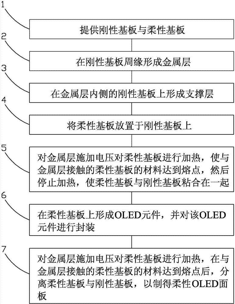
The invention provides a method for manufacturing a flexible OLED panel, comprising: step 1, providing a rigid substrate (20) and a flexible substrate (40); step 2, forming a metal layer (22) on the periphery of the rigid substrate (20); step 3, Form a support layer (24) inside the metal layer (22); step 4, place the flexible substrate (40) on the rigid substrate (20); step 5, apply a voltage to the metal layer (22) to carry out the flexible substrate (40) heating, so that the material of the flexible substrate (40) in contact with the metal layer (22) reaches the melting point, so that the flexible substrate (40) and the rigid substrate (20) are bonded together; step 6, forming an OLED on the flexible substrate (40) element (42), and encapsulate the OLED element (42); step 7, apply voltage to the metal layer (22) to heat the flexible substrate (40), and the flexible substrate (40) in contact with the metal layer (22) After the material reaches the melting point, the flexible substrate (40) and the rigid substrate (20) are separated.
Description
Claims (10)
Priority Applications (6)
| Application Number | Priority Date | Filing Date | Title |
|---|---|---|---|
| CN201310694937.9A CN103682177B (en) | 2013-12-16 | 2013-12-16 | Manufacturing method of flexible OLED panel |
| KR1020167013144A KR101831086B1 (en) | 2013-12-16 | 2014-01-03 | Manufacturing method for flexible oled panel |
| JP2016533562A JP6117998B2 (en) | 2013-12-16 | 2014-01-03 | Method for manufacturing flexible OLED panel |
| GB1607191.2A GB2535064B (en) | 2013-12-16 | 2014-01-03 | Method for manufacturing flexible OLED (organic light emitting diode) panel |
| US14/241,072 US20150171376A1 (en) | 2013-12-16 | 2014-01-03 | Method for manufacturing flexible oled (organic light emitting diode) panel |
| PCT/CN2014/070122 WO2015089918A1 (en) | 2013-12-16 | 2014-01-03 | Manufacturing method for flexible oled panel |
Applications Claiming Priority (1)
| Application Number | Priority Date | Filing Date | Title |
|---|---|---|---|
| CN201310694937.9A CN103682177B (en) | 2013-12-16 | 2013-12-16 | Manufacturing method of flexible OLED panel |
Publications (2)
| Publication Number | Publication Date |
|---|---|
| CN103682177A true CN103682177A (en) | 2014-03-26 |
| CN103682177B CN103682177B (en) | 2015-03-25 |
Family
ID=50319034
Family Applications (1)
| Application Number | Title | Priority Date | Filing Date |
|---|---|---|---|
| CN201310694937.9A Active CN103682177B (en) | 2013-12-16 | 2013-12-16 | Manufacturing method of flexible OLED panel |
Country Status (6)
| Country | Link |
|---|---|
| US (1) | US20150171376A1 (en) |
| JP (1) | JP6117998B2 (en) |
| KR (1) | KR101831086B1 (en) |
| CN (1) | CN103682177B (en) |
| GB (1) | GB2535064B (en) |
| WO (1) | WO2015089918A1 (en) |
Cited By (13)
| Publication number | Priority date | Publication date | Assignee | Title |
|---|---|---|---|---|
| CN104505467A (en) * | 2014-12-05 | 2015-04-08 | 上海天马微电子有限公司 | Composite substrate, manufacturing method of flexible display and flexible display |
| US20150171376A1 (en) * | 2013-12-16 | 2015-06-18 | Shenzhen China Star Optoelectronics Technology Co., Ltd. | Method for manufacturing flexible oled (organic light emitting diode) panel |
| WO2015127762A1 (en) * | 2014-02-28 | 2015-09-03 | 京东方科技集团股份有限公司 | Flexible display substrate motherboard and flexible display substrate manufacturing method |
| CN105024018A (en) * | 2014-04-29 | 2015-11-04 | Tcl集团股份有限公司 | Flexible display and manufacturing method thereof |
| CN105098088A (en) * | 2014-05-05 | 2015-11-25 | Tcl集团股份有限公司 | Flexible display and thin film packaging method thereof |
| CN106328683A (en) * | 2016-10-11 | 2017-01-11 | 武汉华星光电技术有限公司 | Flexible OLED display and the preparing method thereof |
| WO2017020370A1 (en) * | 2015-08-05 | 2017-02-09 | 深圳市华星光电技术有限公司 | Method of manufacturing a flexible display panel and substrate assembly for manufacturing same |
| CN108346612A (en) * | 2017-01-25 | 2018-07-31 | 元太科技工业股份有限公司 | Method for manufacturing flexible electronic device |
| CN109545999A (en) * | 2018-11-21 | 2019-03-29 | 京东方科技集团股份有限公司 | The manufacturing method of initial display device and flexible display panels |
| WO2019061719A1 (en) * | 2017-09-29 | 2019-04-04 | 武汉华星光电半导体显示技术有限公司 | Method for separating flexible oled display and flexible oled display |
| CN109860431A (en) * | 2018-12-12 | 2019-06-07 | 武汉华星光电半导体显示技术有限公司 | Organic Light Emitting Diode (OLED) Panel and Manufacturing Method |
| CN110072336A (en) * | 2018-01-23 | 2019-07-30 | 北京华碳科技有限责任公司 | The method for separating flexible base board and rigid conductive carrier |
| CN115000329A (en) * | 2022-06-29 | 2022-09-02 | 深圳市华星光电半导体显示技术有限公司 | Display panel and mobile terminal |
Families Citing this family (1)
| Publication number | Priority date | Publication date | Assignee | Title |
|---|---|---|---|---|
| CN107195792B (en) * | 2017-05-08 | 2018-11-27 | 武汉华星光电技术有限公司 | The manufacturing device and method of curved face display panel |
Citations (5)
| Publication number | Priority date | Publication date | Assignee | Title |
|---|---|---|---|---|
| US20070059854A1 (en) * | 2005-09-14 | 2007-03-15 | Chin-Jen Huang | Flexible pixel array substrate and method for fabricating the same |
| CN101908555A (en) * | 2009-06-04 | 2010-12-08 | 三星移动显示器株式会社 | Organic light emitting diode display and manufacturing method thereof |
| CN102148330A (en) * | 2010-12-24 | 2011-08-10 | 福建钧石能源有限公司 | Method for manufacturing flexible photoelectric device |
| CN103325731A (en) * | 2013-05-20 | 2013-09-25 | Tcl集团股份有限公司 | Manufacturing method of flexible display device |
| CN103337478A (en) * | 2013-06-26 | 2013-10-02 | 青岛海信电器股份有限公司 | Fabrication method of flexible organic electroluminescence diode display |
Family Cites Families (53)
| Publication number | Priority date | Publication date | Assignee | Title |
|---|---|---|---|---|
| US3512254A (en) * | 1965-08-10 | 1970-05-19 | Corning Glass Works | Method of making an electrical device |
| CA2070654C (en) * | 1990-10-05 | 2003-06-03 | Takuji Okamoto | Process for producing cyclic olefin based polymers, cyclic olefin copolymers, compositions and molded articles comprising the copolymers |
| US5468655A (en) * | 1994-10-31 | 1995-11-21 | Motorola, Inc. | Method for forming a temporary attachment between a semiconductor die and a substrate using a metal paste comprising spherical modules |
| US5756577A (en) * | 1995-03-27 | 1998-05-26 | Grupo Cydsa, S.A. De C.V. | Styrene butadiene copolymer and polyolefin resins based shrink films |
| US6426484B1 (en) * | 1996-09-10 | 2002-07-30 | Micron Technology, Inc. | Circuit and method for heating an adhesive to package or rework a semiconductor die |
| JPH11236457A (en) * | 1998-02-24 | 1999-08-31 | Dainippon Ink & Chem Inc | Shrink film and manufacturing method thereof |
| US20080196828A1 (en) * | 1999-07-14 | 2008-08-21 | Gilbert Michael D | Electrically Disbonding Adhesive Compositions and Related Methods |
| DE19943909A1 (en) * | 1999-09-14 | 2001-03-15 | Wolff Walsrode Ag | Multi-layer co-extruded biaxially stretched high barrier plastic casing with reduced adhesion to the filling material and its use as a food casing |
| AU2001282271A1 (en) * | 2000-08-11 | 2002-02-25 | Anthony John Cooper | Double glazing |
| KR100442830B1 (en) * | 2001-12-04 | 2004-08-02 | 삼성전자주식회사 | Low temperature hermetic sealing method having a passivation layer |
| US7832177B2 (en) * | 2002-03-22 | 2010-11-16 | Electronics Packaging Solutions, Inc. | Insulated glazing units |
| US20040187437A1 (en) * | 2003-03-27 | 2004-09-30 | Stark David H. | Laminated strength-reinforced window assemblies |
| US20040232535A1 (en) * | 2003-05-22 | 2004-11-25 | Terry Tarn | Microelectromechanical device packages with integral heaters |
| DE10337009A1 (en) * | 2003-08-12 | 2005-03-24 | Case Tech Gmbh & Co.Kg | Multilayered coextruded biaxially stretched fiber finished seamless tubular casing and its use as a food casing |
| US20050269943A1 (en) * | 2004-06-04 | 2005-12-08 | Michael Hack | Protected organic electronic devices and methods for making the same |
| KR101141533B1 (en) * | 2005-06-25 | 2012-05-04 | 엘지디스플레이 주식회사 | Substrate transporting method and manufacturing method of flexible display using the same |
| JP2007251080A (en) * | 2006-03-20 | 2007-09-27 | Fujifilm Corp | Fixing method of plastic substrate, circuit board and manufacturing method thereof |
| EP1840648A1 (en) * | 2006-03-31 | 2007-10-03 | Sony Deutschland Gmbh | A method of applying a pattern of metal, metal oxide and/or semiconductor material on a substrate |
| KR100820170B1 (en) * | 2006-08-30 | 2008-04-10 | 한국전자통신연구원 | Stacking method of flexible substrate |
| KR100841376B1 (en) * | 2007-06-12 | 2008-06-26 | 삼성에스디아이 주식회사 | Bonding method and manufacturing method of organic light emitting display device using the same |
| KR100889625B1 (en) * | 2007-07-19 | 2009-03-20 | 삼성모바일디스플레이주식회사 | Bonding method and manufacturing method of organic light emitting display device using the same |
| TWI388078B (en) * | 2008-01-30 | 2013-03-01 | 歐斯朗奧托半導體股份有限公司 | Electronic component manufacturing method and electronic component |
| US7960247B2 (en) * | 2008-04-04 | 2011-06-14 | The Charles Stark Draper Laboratory, Inc. | Die thinning processes and structures |
| TWI354854B (en) * | 2008-09-15 | 2011-12-21 | Ind Tech Res Inst | Substrate structures applied in flexible electrica |
| TWI410329B (en) * | 2009-03-09 | 2013-10-01 | 財團法人工業技術研究院 | Removal device of flexible device and removal method thereof |
| DE102009027283A1 (en) * | 2009-04-03 | 2010-10-07 | Tesa Se | Adhesive film for closing vessels and channels, production and use thereof |
| US8110419B2 (en) * | 2009-08-20 | 2012-02-07 | Integrated Photovoltaic, Inc. | Process of manufacturing photovoltaic device |
| KR101149433B1 (en) * | 2009-08-28 | 2012-05-22 | 삼성모바일디스플레이주식회사 | Flexible display and method for manufacturing the same |
| JP2011113654A (en) * | 2009-11-24 | 2011-06-09 | Toppan Printing Co Ltd | Organic el element and method of manufacturing the same |
| KR101173105B1 (en) * | 2010-05-24 | 2012-08-14 | 한국과학기술원 | Organic light emitting element |
| TWI457614B (en) * | 2010-10-05 | 2014-10-21 | E Ink Holdings Inc | Method for manufacturing flexible color filter substrate |
| TWI486259B (en) * | 2010-12-27 | 2015-06-01 | Au Optronics Corp | Flexible substrate structure and manufacturing method thereof |
| US8816977B2 (en) * | 2011-03-21 | 2014-08-26 | Apple Inc. | Electronic devices with flexible displays |
| US8934228B2 (en) * | 2011-03-21 | 2015-01-13 | Apple Inc. | Display-based speaker structures for electronic devices |
| WO2012129793A1 (en) * | 2011-03-30 | 2012-10-04 | 海洋王照明科技股份有限公司 | Substrate, manufacturing method thereof, and organo-electroluminescent device using the same |
| KR20120138168A (en) * | 2011-06-14 | 2012-12-24 | 삼성디스플레이 주식회사 | Display device and method for manufacturing the same |
| EP2551895B1 (en) * | 2011-07-27 | 2013-11-27 | STMicroelectronics Srl | Method of manufacturing an electronic device having a plastic substrate |
| US20130050227A1 (en) * | 2011-08-30 | 2013-02-28 | Qualcomm Mems Technologies, Inc. | Glass as a substrate material and a final package for mems and ic devices |
| WO2013035298A1 (en) * | 2011-09-08 | 2013-03-14 | シャープ株式会社 | Display device and method for manufacturing same |
| US8723824B2 (en) * | 2011-09-27 | 2014-05-13 | Apple Inc. | Electronic devices with sidewall displays |
| US9125301B2 (en) * | 2011-10-18 | 2015-09-01 | Integrated Microwave Corporation | Integral heater assembly and method for carrier or host board of electronic package assembly |
| CN102636898B (en) * | 2012-03-14 | 2014-03-12 | 京东方科技集团股份有限公司 | Manufacturing method of flexible display devices |
| KR101474949B1 (en) * | 2012-11-01 | 2014-12-22 | 성균관대학교산학협력단 | Method for fabricating the oled using roll to roll processing |
| US9853092B2 (en) * | 2012-11-30 | 2017-12-26 | Lg Display Co., Ltd. | OLED display device having touch sensor and method of manufacturing the same |
| US20140150244A1 (en) * | 2012-11-30 | 2014-06-05 | General Electric Company | Adhesive-free carrier assemblies for glass substrates |
| CN103035490A (en) * | 2012-12-11 | 2013-04-10 | 京东方科技集团股份有限公司 | Preparation method for flexible display device |
| US8912018B2 (en) * | 2012-12-17 | 2014-12-16 | Universal Display Corporation | Manufacturing flexible organic electronic devices |
| TWI505460B (en) * | 2013-02-18 | 2015-10-21 | Innolux Corp | Organic light emitting diode display device and method of manufacturing same |
| KR102133433B1 (en) * | 2013-05-24 | 2020-07-14 | 삼성디스플레이 주식회사 | TFT substrate including barrier layer including silicon oxide layer and silicon silicon nitride layer, Organic light-emitting device comprising the TFT substrate, and the manufacturing method of the TFT substrate |
| CN103384447B (en) * | 2013-06-26 | 2016-06-29 | 友达光电股份有限公司 | Flexible electronic device |
| CN104347449A (en) * | 2013-07-24 | 2015-02-11 | 上海和辉光电有限公司 | A peeling device and peeling method |
| TWI537139B (en) * | 2013-08-30 | 2016-06-11 | 群創光電股份有限公司 | Element substrate, display apparatus and manufacturing method of element substrate |
| CN103682177B (en) * | 2013-12-16 | 2015-03-25 | 深圳市华星光电技术有限公司 | Manufacturing method of flexible OLED panel |
-
2013
- 2013-12-16 CN CN201310694937.9A patent/CN103682177B/en active Active
-
2014
- 2014-01-03 KR KR1020167013144A patent/KR101831086B1/en active Active
- 2014-01-03 US US14/241,072 patent/US20150171376A1/en not_active Abandoned
- 2014-01-03 JP JP2016533562A patent/JP6117998B2/en active Active
- 2014-01-03 GB GB1607191.2A patent/GB2535064B/en active Active
- 2014-01-03 WO PCT/CN2014/070122 patent/WO2015089918A1/en not_active Ceased
Patent Citations (5)
| Publication number | Priority date | Publication date | Assignee | Title |
|---|---|---|---|---|
| US20070059854A1 (en) * | 2005-09-14 | 2007-03-15 | Chin-Jen Huang | Flexible pixel array substrate and method for fabricating the same |
| CN101908555A (en) * | 2009-06-04 | 2010-12-08 | 三星移动显示器株式会社 | Organic light emitting diode display and manufacturing method thereof |
| CN102148330A (en) * | 2010-12-24 | 2011-08-10 | 福建钧石能源有限公司 | Method for manufacturing flexible photoelectric device |
| CN103325731A (en) * | 2013-05-20 | 2013-09-25 | Tcl集团股份有限公司 | Manufacturing method of flexible display device |
| CN103337478A (en) * | 2013-06-26 | 2013-10-02 | 青岛海信电器股份有限公司 | Fabrication method of flexible organic electroluminescence diode display |
Cited By (24)
| Publication number | Priority date | Publication date | Assignee | Title |
|---|---|---|---|---|
| US20150171376A1 (en) * | 2013-12-16 | 2015-06-18 | Shenzhen China Star Optoelectronics Technology Co., Ltd. | Method for manufacturing flexible oled (organic light emitting diode) panel |
| US9577202B2 (en) | 2014-02-28 | 2017-02-21 | Boe Technology Group Co., Ltd. | Flexible display substrate mother board and method of manufacturing flexible display substrate |
| WO2015127762A1 (en) * | 2014-02-28 | 2015-09-03 | 京东方科技集团股份有限公司 | Flexible display substrate motherboard and flexible display substrate manufacturing method |
| CN105024018A (en) * | 2014-04-29 | 2015-11-04 | Tcl集团股份有限公司 | Flexible display and manufacturing method thereof |
| CN105024018B (en) * | 2014-04-29 | 2018-05-08 | Tcl集团股份有限公司 | A kind of flexible display and preparation method thereof |
| CN105098088A (en) * | 2014-05-05 | 2015-11-25 | Tcl集团股份有限公司 | Flexible display and thin film packaging method thereof |
| CN104505467B (en) * | 2014-12-05 | 2017-09-19 | 上海天马微电子有限公司 | Composite substrate, manufacturing method of flexible display and flexible display |
| CN104505467A (en) * | 2014-12-05 | 2015-04-08 | 上海天马微电子有限公司 | Composite substrate, manufacturing method of flexible display and flexible display |
| WO2017020370A1 (en) * | 2015-08-05 | 2017-02-09 | 深圳市华星光电技术有限公司 | Method of manufacturing a flexible display panel and substrate assembly for manufacturing same |
| WO2018068380A1 (en) * | 2016-10-11 | 2018-04-19 | 武汉华星光电技术有限公司 | Flexible oled display and manufacturing method therefor |
| CN106328683A (en) * | 2016-10-11 | 2017-01-11 | 武汉华星光电技术有限公司 | Flexible OLED display and the preparing method thereof |
| CN106328683B (en) * | 2016-10-11 | 2019-04-30 | 武汉华星光电技术有限公司 | Flexible OLED display and method of making the same |
| CN108346612A (en) * | 2017-01-25 | 2018-07-31 | 元太科技工业股份有限公司 | Method for manufacturing flexible electronic device |
| CN108346612B (en) * | 2017-01-25 | 2022-01-25 | 元太科技工业股份有限公司 | Method for manufacturing flexible electronic device |
| US11191166B2 (en) | 2017-01-25 | 2021-11-30 | E Ink Holdings Inc. | Fabrication method of flexible electronic device |
| WO2019061719A1 (en) * | 2017-09-29 | 2019-04-04 | 武汉华星光电半导体显示技术有限公司 | Method for separating flexible oled display and flexible oled display |
| CN110072336B (en) * | 2018-01-23 | 2020-11-06 | 北京华碳科技有限责任公司 | Method for separating flexible substrate and rigid conductive carrier |
| CN110072336A (en) * | 2018-01-23 | 2019-07-30 | 北京华碳科技有限责任公司 | The method for separating flexible base board and rigid conductive carrier |
| CN109545999B (en) * | 2018-11-21 | 2021-05-04 | 京东方科技集团股份有限公司 | Initial display device and manufacturing method of flexible display panel |
| CN109545999A (en) * | 2018-11-21 | 2019-03-29 | 京东方科技集团股份有限公司 | The manufacturing method of initial display device and flexible display panels |
| WO2020118846A1 (en) * | 2018-12-12 | 2020-06-18 | 武汉华星光电半导体显示技术有限公司 | Organic light-emitting diode (oled) panel and manufacturing method therefor |
| CN109860431A (en) * | 2018-12-12 | 2019-06-07 | 武汉华星光电半导体显示技术有限公司 | Organic Light Emitting Diode (OLED) Panel and Manufacturing Method |
| CN115000329A (en) * | 2022-06-29 | 2022-09-02 | 深圳市华星光电半导体显示技术有限公司 | Display panel and mobile terminal |
| CN115000329B (en) * | 2022-06-29 | 2024-11-12 | 深圳市华星光电半导体显示技术有限公司 | Display panel and mobile terminal |
Also Published As
| Publication number | Publication date |
|---|---|
| GB2535064B (en) | 2019-12-04 |
| KR101831086B1 (en) | 2018-02-21 |
| JP6117998B2 (en) | 2017-04-19 |
| US20150171376A1 (en) | 2015-06-18 |
| WO2015089918A1 (en) | 2015-06-25 |
| CN103682177B (en) | 2015-03-25 |
| KR20160074593A (en) | 2016-06-28 |
| GB2535064A (en) | 2016-08-10 |
| JP2016537788A (en) | 2016-12-01 |
Similar Documents
| Publication | Publication Date | Title |
|---|---|---|
| CN103682177A (en) | Manufacturing method of flexible OLED panel | |
| CN106711355B (en) | The production method of flexible OLED display panel | |
| CN105514302B (en) | Light emitting diode with quantum dots sub-pix array, its manufacture method and display device | |
| TWI595643B (en) | Double-sided display, double-sided display control device and method of manufacturing same | |
| CN108666349B (en) | Color filter substrate, manufacturing method thereof and WOLED display | |
| CN106449711A (en) | Flexible AMOLED display device preparation method | |
| US20160343791A1 (en) | Double side oled display device and manufacture method thereof | |
| CN107644891A (en) | The preparation method of flexible OLED panel | |
| WO2018086211A1 (en) | Flexible tft base plate and fabrication method therefor | |
| US10243163B2 (en) | Flexible OLED display and manufacturing method thereof | |
| US9679953B2 (en) | WOLED back panel and method of manufacturing the same | |
| CN104538421B (en) | Oled display substrate and its manufacturing method | |
| CN107845665A (en) | Organic electroluminescence display device and method of manufacturing same and preparation method | |
| CN108417726A (en) | OLED device and manufacturing method thereof | |
| Yin et al. | Color-stable WRGB emission from blue OLEDs with quantum dots-based patterned down-conversion layer | |
| JP6373382B2 (en) | Method for manufacturing anode connection structure of organic light emitting diode | |
| CN107799017A (en) | Display with double faces and preparation method thereof | |
| CN203787434U (en) | Organic Light Emitting Diode Display Panel | |
| CN103972268B (en) | Organic LED display panel and preparation method thereof | |
| US20160181574A1 (en) | Method for manufacturing flexible oled (organic light emitting diode) panel | |
| CN1992374B (en) | Method of fabricating organic electroluminescent display device | |
| KR101658438B1 (en) | Substrate Bonding Apparatus for Organic Electro Luminescent device | |
| US20160133841A1 (en) | Method of manufacturing organic light emitting diode display | |
| CN107749418A (en) | A kind of processing technology of the organic light emission layer assembly of double-side display device | |
| CN103560211A (en) | Method for manufacturing organic electroluminescence device and manufactured organic electroluminescence device |
Legal Events
| Date | Code | Title | Description |
|---|---|---|---|
| PB01 | Publication | ||
| PB01 | Publication | ||
| C10 | Entry into substantive examination | ||
| SE01 | Entry into force of request for substantive examination | ||
| C14 | Grant of patent or utility model | ||
| GR01 | Patent grant | ||
| C41 | Transfer of patent application or patent right or utility model | ||
| TR01 | Transfer of patent right |
Effective date of registration: 20160127 Address after: 430070 Hubei City, Wuhan Province, East Lake Development Zone, high tech Avenue, No. 666 biological city building C5 Patentee after: Wuhan Hua Xing photoelectricity technology corporation, Ltd. Address before: 518132 Guangming Road, Guangdong, Shenzhen Province, Ming Road, No. 2 - No. 9 Patentee before: Shenzhen Huaxing Optoelectronic Technology Co., Ltd. |
|
| TR01 | Transfer of patent right | ||
| TR01 | Transfer of patent right |
Effective date of registration: 20190220 Address after: 430079 Room 305, Building C5, Guanggu Biological Innovation Park, 666 High-tech Avenue, Donghu New Technology Development Zone, Wuhan City, Hubei Province Patentee after: Wuhan Huaxing photoelectric semiconductor display technology Co., Ltd. Address before: 430070 C5 Biological City, 666 High-tech Avenue, Donghu Development Zone, Wuhan City, Hubei Province Patentee before: Wuhan Hua Xing photoelectricity technology corporation, Ltd. |