CN102636898B - Manufacturing method of flexible display devices - Google Patents
Manufacturing method of flexible display devices Download PDFInfo
- Publication number
- CN102636898B CN102636898B CN201210067188.2A CN201210067188A CN102636898B CN 102636898 B CN102636898 B CN 102636898B CN 201210067188 A CN201210067188 A CN 201210067188A CN 102636898 B CN102636898 B CN 102636898B
- Authority
- CN
- China
- Prior art keywords
- substrate
- release layer
- flexible substrate
- flexible
- transparent hard
- Prior art date
- Legal status (The legal status is an assumption and is not a legal conclusion. Google has not performed a legal analysis and makes no representation as to the accuracy of the status listed.)
- Expired - Fee Related
Links
Images


Classifications
-
- G—PHYSICS
- G02—OPTICS
- G02F—OPTICAL DEVICES OR ARRANGEMENTS FOR THE CONTROL OF LIGHT BY MODIFICATION OF THE OPTICAL PROPERTIES OF THE MEDIA OF THE ELEMENTS INVOLVED THEREIN; NON-LINEAR OPTICS; FREQUENCY-CHANGING OF LIGHT; OPTICAL LOGIC ELEMENTS; OPTICAL ANALOGUE/DIGITAL CONVERTERS
- G02F1/00—Devices or arrangements for the control of the intensity, colour, phase, polarisation or direction of light arriving from an independent light source, e.g. switching, gating or modulating; Non-linear optics
- G02F1/01—Devices or arrangements for the control of the intensity, colour, phase, polarisation or direction of light arriving from an independent light source, e.g. switching, gating or modulating; Non-linear optics for the control of the intensity, phase, polarisation or colour
- G02F1/13—Devices or arrangements for the control of the intensity, colour, phase, polarisation or direction of light arriving from an independent light source, e.g. switching, gating or modulating; Non-linear optics for the control of the intensity, phase, polarisation or colour based on liquid crystals, e.g. single liquid crystal display cells
- G02F1/133—Constructional arrangements; Operation of liquid crystal cells; Circuit arrangements
- G02F1/1333—Constructional arrangements; Manufacturing methods
- G02F1/133305—Flexible substrates, e.g. plastics, organic film
-
- H—ELECTRICITY
- H10—SEMICONDUCTOR DEVICES; ELECTRIC SOLID-STATE DEVICES NOT OTHERWISE PROVIDED FOR
- H10K—ORGANIC ELECTRIC SOLID-STATE DEVICES
- H10K59/00—Integrated devices, or assemblies of multiple devices, comprising at least one organic light-emitting element covered by group H10K50/00
- H10K59/10—OLED displays
- H10K59/12—Active-matrix OLED [AMOLED] displays
- H10K59/1201—Manufacture or treatment
-
- H—ELECTRICITY
- H10—SEMICONDUCTOR DEVICES; ELECTRIC SOLID-STATE DEVICES NOT OTHERWISE PROVIDED FOR
- H10K—ORGANIC ELECTRIC SOLID-STATE DEVICES
- H10K71/00—Manufacture or treatment specially adapted for the organic devices covered by this subclass
- H10K71/80—Manufacture or treatment specially adapted for the organic devices covered by this subclass using temporary substrates
-
- H—ELECTRICITY
- H10—SEMICONDUCTOR DEVICES; ELECTRIC SOLID-STATE DEVICES NOT OTHERWISE PROVIDED FOR
- H10K—ORGANIC ELECTRIC SOLID-STATE DEVICES
- H10K2102/00—Constructional details relating to the organic devices covered by this subclass
- H10K2102/301—Details of OLEDs
- H10K2102/311—Flexible OLED
-
- H—ELECTRICITY
- H10—SEMICONDUCTOR DEVICES; ELECTRIC SOLID-STATE DEVICES NOT OTHERWISE PROVIDED FOR
- H10K—ORGANIC ELECTRIC SOLID-STATE DEVICES
- H10K77/00—Constructional details of devices covered by this subclass and not covered by groups H10K10/80, H10K30/80, H10K50/80 or H10K59/80
- H10K77/10—Substrates, e.g. flexible substrates
- H10K77/111—Flexible substrates
Landscapes
- Physics & Mathematics (AREA)
- Nonlinear Science (AREA)
- Engineering & Computer Science (AREA)
- Manufacturing & Machinery (AREA)
- Crystallography & Structural Chemistry (AREA)
- Chemical & Material Sciences (AREA)
- Mathematical Physics (AREA)
- General Physics & Mathematics (AREA)
- Optics & Photonics (AREA)
- Devices For Indicating Variable Information By Combining Individual Elements (AREA)
- Microelectronics & Electronic Packaging (AREA)
- Liquid Crystal (AREA)
- Laminated Bodies (AREA)
Abstract
本发明提供一种柔性显示装置的制备方法,所述制备方法包括:在透明硬质基板上形成离型层,所述离型层的材料为添加有惰性物质的紫外光分解材料;将柔性基板结合到形成有离型层的透明硬质基板上,其中,柔性基板与透明硬质基板上形成有离型层的一侧相对;在所述柔性基板上形成显示器件;从所述透明硬质基板的远离离型层的一侧照射紫外线,以引发所述离型层发生释放出气体的光化学反应,使得所述透明硬质基板与所述柔性基板分离。本发明能够简化柔性显示装置的生产工艺。
The invention provides a method for preparing a flexible display device. The preparation method includes: forming a release layer on a transparent hard substrate, and the material of the release layer is an ultraviolet light decomposition material added with an inert substance; Bonded to a transparent hard substrate with a release layer, wherein the flexible substrate is opposite to the side where the release layer is formed on the transparent hard substrate; a display device is formed on the flexible substrate; from the transparent hard The side of the substrate away from the release layer is irradiated with ultraviolet rays to trigger a photochemical reaction in the release layer that releases gas, so that the transparent hard substrate is separated from the flexible substrate. The invention can simplify the production process of the flexible display device.
Description
技术领域 technical field
本发明涉及一种柔性显示装置的制备方法,特别是基于紫外光分解材料与紫外线反应特性的柔性显示装置的贴覆和分离方法。The invention relates to a method for preparing a flexible display device, in particular to a method for attaching and separating a flexible display device based on the ultraviolet light decomposition material and ultraviolet reaction characteristics.
背景技术 Background technique
液晶显示器(LCD)技术在近十年有了飞速地发展,从屏幕的尺寸到显示的质量都取得了很大进步。经过不断的努力,LCD各方面的性能已经达到了传统阴极射线管显示器(CRT)的水平,大有取代CRT的趋势。Liquid crystal display (LCD) technology has developed rapidly in the past ten years, and great progress has been made in terms of screen size and display quality. After continuous efforts, the performance of LCD in all aspects has reached the level of traditional cathode ray tube display (CRT), and it has a tendency to replace CRT.
随着LCD生产的不断扩大,各个生产厂商之间的竞争也日趋激烈。各厂家在不断努力降低产品的生产成本的同时,也在不断提高产品性能,以及增加更多功能,从而提高产品的附加值和提升市场的竞争力。With the continuous expansion of LCD production, the competition among various manufacturers is becoming increasingly fierce. While manufacturers are constantly striving to reduce the production cost of products, they are also constantly improving product performance and adding more functions, thereby increasing the added value of products and enhancing market competitiveness.
柔性显示产品凭借其独特的外形特点,与人性化的使用方式,具有巨大的市场潜力。目前柔性显示产品的制备方法主要分为两类。第一类是采用卷对卷的方法(roll to roll),通过印刷直接在柔性基板上制备显示器件,但是由于印刷技术所限,只能制备一些低精度要求的产品(如射频身份证RFID),且成品率和可信赖性较差。第二类是采用贴覆取下的方法,将柔性基板贴覆在硬质背板上制备显示产品,制备完成显示器件之后再取下硬质背板。这种方法精度较高,制造设备与传统TFT-LCD阵列制造设备相仿,因此短期内更接近于量产应用。Flexible display products have huge market potential due to their unique appearance and humanized use. At present, the preparation methods of flexible display products are mainly divided into two categories. The first type is to use the roll-to-roll method (roll to roll) to prepare display devices directly on the flexible substrate by printing, but due to the limitation of printing technology, only some products with low precision requirements can be prepared (such as radio frequency ID card RFID) , and the yield and reliability are poor. The second type is to adopt the method of pasting and removing, and the flexible substrate is pasted on the hard backplane to prepare display products, and the hard backplane is removed after the display device is prepared. This method has high precision, and the manufacturing equipment is similar to the traditional TFT-LCD array manufacturing equipment, so it is closer to mass production applications in the short term.
采用贴覆取下方式目前的方法是采用粘接剂将有机塑料基板贴覆在玻璃基板上,制备完成显示器件后,在其背面采用高能激光束扫描的方法,使得粘接剂发生养生老化,粘着性能下降,从而使得有机塑料基板能够从玻璃基板上剥离下来。但是这种方法由于需要高能激光束扫描,生产效率较低,且剥离的均匀性较差。The current method of sticking and removing is to use an adhesive to stick the organic plastic substrate on the glass substrate. After the display device is prepared, a high-energy laser beam is used to scan the back of the display to make the adhesive aging. Adhesive properties are reduced, allowing the organic plastic substrate to be peeled off from the glass substrate. However, due to the need for high-energy laser beam scanning, this method has low production efficiency and poor peeling uniformity.
发明内容 Contents of the invention
本发明所要解决的技术问题是提供一种柔性显示装置的制备方法,以简化柔性显示装置的生产工艺。The technical problem to be solved by the present invention is to provide a method for preparing a flexible display device, so as to simplify the production process of the flexible display device.
为解决上述技术问题,本发明提供技术方案如下:In order to solve the problems of the technologies described above, the present invention provides technical solutions as follows:
一种柔性显示装置的制备方法,包括:A method for preparing a flexible display device, comprising:
在透明硬质基板上形成离型层,所述离型层的材料为添加有惰性物质的紫外光分解材料;A release layer is formed on the transparent hard substrate, and the material of the release layer is an ultraviolet light decomposition material added with an inert substance;
将柔性基板结合到形成有离型层的透明硬质基板上,其中,柔性基板与透明硬质基板上形成有离型层的一侧相对;bonding the flexible substrate to the transparent rigid substrate formed with a release layer, wherein the flexible substrate is opposite to the side on which the release layer is formed on the transparent rigid substrate;
在所述柔性基板上形成显示器件;以及forming a display device on the flexible substrate; and
从所述透明硬质基板的远离离型层的一侧照射紫外线,以引发所述离型层发生释放出气体的光化学反应,使得所述透明硬质基板与所述柔性基板分离。Irradiating ultraviolet rays from the side of the transparent hard substrate away from the release layer to trigger a photochemical reaction in the release layer to release gas, so that the transparent hard substrate is separated from the flexible substrate.
上述的制备方法,其中,所述将柔性基板结合到形成有离型层的透明硬质基板上,包括:The above preparation method, wherein said bonding the flexible substrate to the transparent hard substrate formed with a release layer, comprises:
在形成有离型层的透明硬质基板上涂覆粘接剂;Coating an adhesive on the transparent hard substrate with a release layer;
将柔性基板贴覆到涂覆有粘接剂的透明硬质基板上。Attach the flexible substrate to the transparent rigid substrate coated with adhesive.
上述的制备方法,其中:The above-mentioned preparation method, wherein:
所述惰性物质的全部或部分为粘接剂;All or part of the inert substance is a binder;
所述将柔性基板结合到形成有离型层的透明硬质基板上为:将柔性基板直接贴覆到的形成有离型层的透明硬质基板上。The bonding of the flexible substrate to the transparent rigid substrate formed with the release layer is: directly attaching the flexible substrate to the transparent rigid substrate formed with the release layer.
上述的制备方法,其中,所述紫外光分解材料为:The above-mentioned preparation method, wherein, the ultraviolet light decomposing material is:
高氯酸·3(5)-氨基-4-肼基-1,2,4-三唑铜或过氯酰胺。Perchloric acid · 3(5)-amino-4-hydrazino-1,2,4-triazole copper or perchloramide.
上述的制备方法,其中,所述惰性物质为:The above-mentioned preparation method, wherein, the inert substance is:
聚酰亚胺、丙烯酸酯、二氧化硅、氮化硅、氧化锆或氧化钛。Polyimide, acrylate, silica, silicon nitride, zirconia or titania.
上述的制备方法,其中:The above-mentioned preparation method, wherein:
所述透明硬质基板为无色玻璃基板,或者,其颜色不含黄色成分的玻璃基板。The transparent hard substrate is a colorless glass substrate, or a glass substrate whose color does not contain yellow components.
上述的制备方法,其中:所述柔性基板为黄色柔性基板。The above preparation method, wherein: the flexible substrate is a yellow flexible substrate.
上述的制备方法,其中,所述柔性基板的材料为:The above preparation method, wherein the material of the flexible substrate is:
聚酰亚胺、聚奈二甲酸乙二酯、聚对苯二甲酸乙二醇酯、纤维强化塑料、聚醚砜、聚芳酯、聚碳酸酯中的一种或一种以上的组合。One or a combination of polyimide, polyethylene naphthalate, polyethylene terephthalate, fiber reinforced plastics, polyethersulfone, polyarylate, polycarbonate.
上述的制备方法,其中:所述粘接剂为压敏胶或热敏胶。The above preparation method, wherein: the adhesive is pressure-sensitive adhesive or heat-sensitive adhesive.
上述的制备方法,其中:在从所述透明硬质基板的远离离型层的一侧照射紫外线,以引发所述离型层发生释放出气体的光化学反应,使得所述透明硬质基板与所述柔性基板分离之前,并且在在所述柔性基板上形成显示器件之后,还包括:The above-mentioned preparation method, wherein: irradiate ultraviolet rays from the side away from the release layer of the transparent hard substrate to trigger a photochemical reaction in which the release layer releases gas, so that the transparent hard substrate and the Before the flexible substrate is separated, and after the display device is formed on the flexible substrate, it also includes:
进行切割工艺。Carry out the cutting process.
与现有技术相比,本发明采用将紫外光分解材料中添加惰性物质制备离型层,与柔性基板相配合,通过贴覆取下的方式制备柔性显示装置,从而可以采用非常接近传统TFT-LCD阵列基板的生产方法低温制备柔性显示产品,简化了生产工艺,降低了柔性显示产品设备的生产成本。Compared with the prior art, the present invention adopts the method of adding inert substances to the ultraviolet light decomposition material to prepare the release layer, and cooperates with the flexible substrate to prepare a flexible display device by attaching and removing it, so that the flexible display device can be used very close to the traditional TFT- The production method of the LCD array substrate prepares the flexible display product at low temperature, simplifies the production process, and reduces the production cost of the flexible display product equipment.
附图说明 Description of drawings
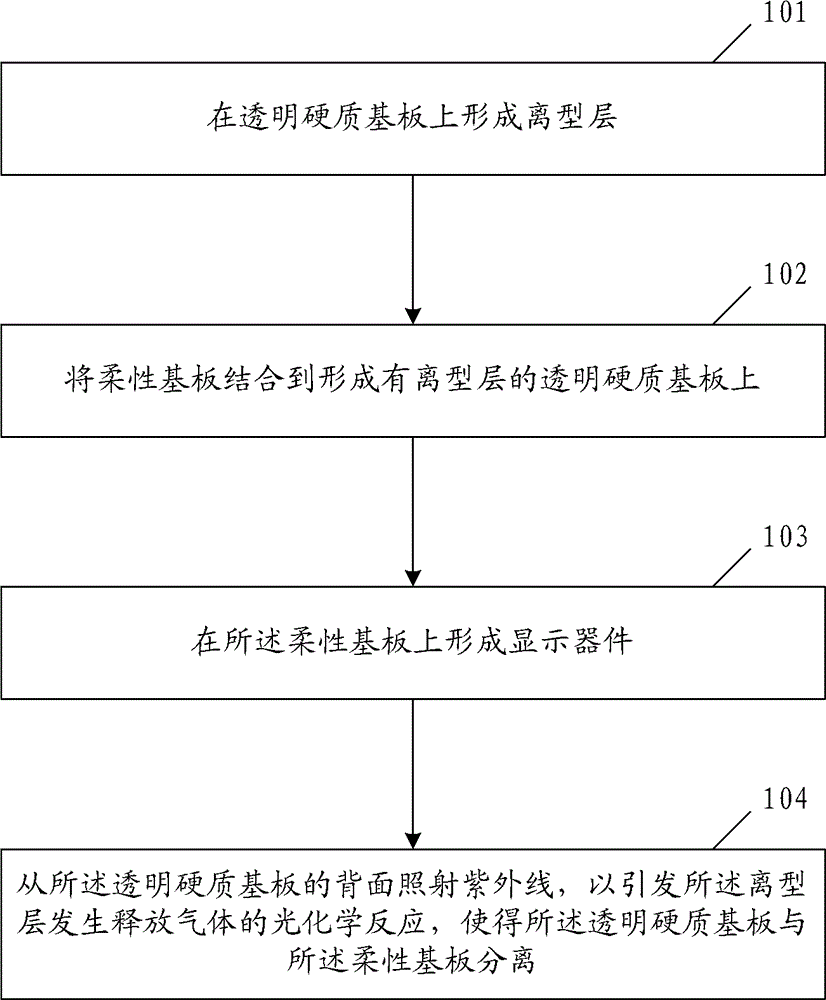
图1为本发明实施例的柔性显示装置的制备方法流程图;FIG. 1 is a flowchart of a method for manufacturing a flexible display device according to an embodiment of the present invention;
图2为本发明实施例中离型层材料的涂覆示意图;Fig. 2 is the coating schematic diagram of release layer material in the embodiment of the present invention;
图3为本发明实施例中粘接剂的涂覆示意图;Fig. 3 is the coating schematic diagram of adhesive in the embodiment of the present invention;
图4为本发明实施例中柔性基板的贴覆示意图;Fig. 4 is a schematic diagram of the lamination of the flexible substrate in the embodiment of the present invention;
图5为本发明实施例中显示器件的制备示意图;5 is a schematic diagram of the preparation of a display device in an embodiment of the present invention;
图6为本发明实施例中紫外线背面照射离型层示意图;Fig. 6 is a schematic diagram of the release layer irradiated by ultraviolet rays on the back of the embodiment of the present invention;
图7为本发明实施例中分离后的柔性显示装置示意图。FIG. 7 is a schematic diagram of a separated flexible display device in an embodiment of the present invention.
附图标记:Reference signs:
1、透明硬质基板;2、离型层;3、粘接剂;4、柔性基板;5、显示器件;6、正面照射紫外线;7、背面照射紫外线。1. Transparent rigid substrate; 2. Release layer; 3. Adhesive; 4. Flexible substrate; 5. Display device; 6. UV radiation from the front; 7. UV radiation from the back.
具体实施方式 Detailed ways
为使本发明的目的、技术方案和优点更加清楚,下面将结合附图及具体实施例对本发明进行详细描述。In order to make the object, technical solution and advantages of the present invention clearer, the present invention will be described in detail below with reference to the accompanying drawings and specific embodiments.
紫外光分解材料是一种遇紫外线发生光化学反应的材料,反应产物包含气体成份。本发明实施例提供一种柔性显示装置的制备方法,采用将紫外光分解材料中添加大量惰性物质(与其不发生反应的物质)制备离型层,与柔性基板相配合,通过贴覆取下的方式制备柔性显示装置,从而可以采用非常接近传统TFT-LCD阵列基板的生产方法低温制备柔性显示产品,达到降低柔性显示产品设备生产成本的作用。The ultraviolet light decomposition material is a material that undergoes a photochemical reaction when exposed to ultraviolet light, and the reaction product contains gas components. The embodiment of the present invention provides a method for preparing a flexible display device. A release layer is prepared by adding a large amount of inert substances (substances that do not react with it) to the ultraviolet light decomposition material, which is matched with a flexible substrate and removed by pasting. The flexible display device can be prepared in this way, so that the flexible display product can be prepared at a low temperature using a production method very close to the traditional TFT-LCD array substrate, so as to reduce the production cost of the flexible display product equipment.
参照图7,本发明实施例制备的柔性显示装置可以包括:柔性基板4、形成在柔性基板4上的显示器件5。其中,所述显示器件5可以为胆甾醇型LCD、有机发光器件OLED、电泳器件或聚合物分散型液晶PDLC等。Referring to FIG. 7 , the flexible display device prepared by the embodiment of the present invention may include: a flexible substrate 4 and a display device 5 formed on the flexible substrate 4 . Wherein, the display device 5 may be a cholesteric LCD, an organic light emitting device OLED, an electrophoretic device or a polymer dispersed liquid crystal PDLC, and the like.
参照图1,上述柔性显示装置的制备方法,可以包括如下步骤:Referring to FIG. 1, the method for preparing the above-mentioned flexible display device may include the following steps:
步骤101:在透明硬质基板1上形成离型层2;Step 101: forming a
所述透明硬质基板1可以采用无色玻璃基板,或者,其颜色不含黄色成分的玻璃基板。在后续步骤中,需要在玻璃基板背面照射紫外线,使得紫外线穿透玻璃基板到达离型层2,以引发离型层2发生释放出气体的光化学反应。而黄色会吸收紫外线,使得紫外线无法穿透,因此,本发明实施例中采用的透明硬质基板不含有黄色成分。The transparent
所述离型层2的材料为添加有惰性物质的紫外光分解材料。所述紫外光分解材料可以采用:高氯酸·3(5)-氨基-4-肼基-1,2,4-三唑铜,或过氯酰胺,或二者的组合。所述惰性物质可以采用:聚酰亚胺、丙烯酸酯、二氧化硅或氮化硅、氧化锆、氧化钛等与离型层材料不发生化学反应的物质,实际使用时,可以采用上述物质中的一种或任意两种以上的组合。The material of the
本步骤中,首先是在紫外光分解材料中添加大量惰性物质来制备离型层材料,然后将离型层材料涂覆在透明硬质基板上1来形成离型层2(如图2所示)。In this step, at first, a large amount of inert substances are added to the ultraviolet light decomposition material to prepare the release layer material, and then the release layer material is coated on the transparent
步骤102:将柔性基板4结合到形成有离型层2的透明硬质基板1上,其中,柔性基板4与透明硬质基板1上形成有离型层的一侧相对;Step 102: bonding the flexible substrate 4 to the transparent
所述柔性基板4可以采用聚酰亚胺PI,或经过改性、染色处理后为黄色的材料,如黄色的聚奈二甲酸乙二酯PEN,聚对苯二甲酸乙二醇酯PET,纤维强化塑料FRP,聚醚砜PES,聚芳酯PAR,聚碳酸酯PC等;也可以为上述材料中的多种材料组合成的复合膜层。The flexible substrate 4 can be polyimide PI, or a yellow material after modification and dyeing, such as yellow polyethylene naphthalate PEN, polyethylene terephthalate PET, fiber Reinforced plastic FRP, polyethersulfone PES, polyarylate PAR, polycarbonate PC, etc.; it can also be a composite film layer composed of multiple materials in the above materials.
本发明实施例提供如下两种结合的方式。The embodiment of the present invention provides the following two combinations.
方式1
首先,如图3所示,在形成有离型层2的透明硬质基板1上涂覆粘接剂3;First, as shown in FIG. 3 , an adhesive 3 is coated on a transparent
然后,如图4所示,将柔性基板4贴覆到涂覆有粘接剂3的透明硬质基板上1。可选地,通过加压或加热的方式使得粘接剂3固化,从而使得柔性基板4与透明硬质基板1能够均匀平整地贴覆在一起。Then, as shown in FIG. 4 , the flexible substrate 4 is attached to the transparent
此种方式中,优选地,应保证离型层2完全位于柔性基板4的下方且其面积小于柔性基板4的面积,柔性基板4下方不存在离型层的区域以及离型层2的上方均涂覆有粘结剂3。这一优选方案通过使在柔性基板4下方不存在离型层的区域涂覆有粘结剂3,可以保证柔性基板4与透明硬质基板1保持紧密结合,防止在后续柔性显示装置的制备中柔性基板与硬质透明基板之间发生意外脱离,并且可以防止后续柔性显示装置的制备中在刻蚀过程中各种酸液等对离型层2的腐蚀。In this way, preferably, it should be ensured that the
方式2
在制备离型层材料时,在紫外光分解材料中添加的惰性物质全部或部分采用粘接剂材料,这样,粘结剂材料和离型层材料作为一体,可以一次性进行涂覆来形成离型层2。然后,就可以将柔性基板4直接贴覆到的形成有离型层2的透明硬质基板1上。可见,方式2相比于方式1,工艺更加简单。When preparing the release layer material, all or part of the inert material added to the ultraviolet light decomposition material uses an adhesive material, so that the adhesive material and the release layer material are integrated and can be coated at one time to form a release layer.
其中,所述粘接剂3可以采用压敏胶或热敏胶,不采用光敏胶,例如,可以采用丙烯酸酯压敏胶。Wherein, the adhesive 3 may use pressure-sensitive adhesive or heat-sensitive adhesive instead of photosensitive adhesive, for example, acrylate pressure-sensitive adhesive may be used.
在此方式中,通过粘结剂材料和离型层材料作为一体一次性进行涂覆来形成的离型层2,优选地为完全位于柔性基板4的下方且其面积等于柔性基板4的面积。这一优选方案既可以保证柔性基板4与透明硬质基板1的紧密结合(面积小则可能导致结合不紧密),又可以保证不浪费粘结剂材料和离型层材料(面积大则会造成粘结剂材料和离型层材料的浪费)。In this way, the
步骤103:在所述柔性基板4上形成显示器件5;Step 103: forming a display device 5 on the flexible substrate 4;
参照图5,可以按照传统的成膜、光刻、刻蚀方法,来制备显示器件5的阵列基板。由于柔性基板4是黄色的,而黄色会吸收紫外线,因此在制备阵列基板或的过程中的紫外线6无法穿过柔性基板4到达离型层2,离型层2在显示器件5的制备过程中始终保持未引发状态。Referring to FIG. 5 , the array substrate of the display device 5 can be prepared according to conventional film formation, photolithography, and etching methods. Since the flexible substrate 4 is yellow, and yellow can absorb ultraviolet rays, the ultraviolet rays 6 in the process of preparing the array substrate or the array substrate cannot pass through the flexible substrate 4 to reach the
步骤104:从所述透明硬质基板1的远离离型层2的一侧照射紫外线7,以引发所述离型层2发生释放出气体的光化学反应,使得所述透明硬质基板1与所述柔性基板3分离。Step 104: irradiate ultraviolet light 7 from the side of the transparent
当整个显示器件5制备完成后,从透明硬质基板1背面照着紫外光分解材料敏感波长的紫外线7(参照图6),引发离型层2中的炸药组分,从而使得透明硬质基板1与柔性基板3分离(参照图7)。由于含有大量惰性物质,因此对柔性基板4和粘接剂3虽然有一定冲击性,但不至于使得柔性基板4发生非弹性形变(屈服)。After the whole display device 5 is prepared, the ultraviolet light 7 (referring to Fig. 6 ) of the sensitive wavelength of the ultraviolet light decomposition material is illuminated from the back of the transparent
需要说明的是,在显示器件制备工艺中,显示器件制备完成后一张基板(对应本发明实施例的柔性基板)上一般制备有一个或多个面板(即panel,对应于本发明实施例所述的柔性显示装置),无论在一张基板上制备一个还是多个panel,最后一般都需要经过切割工艺,以切割出最终用于模组组装的panel。在本发明实施例中,切割工艺一般也是显示器件5制备完成后不可缺少的步骤,以切割出用于模组装置等后续工艺的柔性显示装置。本发明实施中,也可以包括切割工艺;并且,步骤104即“使得透明硬质基板1与柔性基板4分离的工艺过程”,可以在切割前进行,也可以在切割后进行。优选地,是在切割后进行分离,因为通过适当控制切割位置可以将粘结剂切掉一部分,尤其当步骤102中通过“方式1”进行时,可以通过合理确定切割位置将不存在离型层的区域涂覆的粘结剂切割掉,进而更易于透明硬质基板1与柔性基板4分离。It should be noted that, in the manufacturing process of the display device, one or more panels (ie, panels, corresponding to the flexible substrate in the embodiment of the present invention) are generally prepared on one substrate (corresponding to the flexible substrate in the embodiment of the present invention) after the display device is prepared. The above-mentioned flexible display device), no matter one or more panels are prepared on a substrate, it generally needs to go through a cutting process in the end to cut out the final panels for module assembly. In the embodiment of the present invention, the cutting process is generally an indispensable step after the display device 5 is manufactured, so as to cut out a flexible display device for subsequent processes such as a module device. In the implementation of the present invention, a cutting process may also be included; and step 104, namely "the process of separating the transparent
由于大面积紫外线辐照设备已经在液晶显示领域广泛采用,因此采用本发明实施例的方法,可以在低温环境下简单、均匀、快速实现柔性基板的贴覆、显示器件的制备和柔性基板的取下,从而提高了生产效率和产品品质。Since large-area ultraviolet irradiation equipment has been widely used in the field of liquid crystal display, the method of the embodiment of the present invention can simply, uniformly and quickly realize the lamination of flexible substrates, the preparation of display devices and the removal of flexible substrates in a low temperature environment. , thereby improving production efficiency and product quality.
在本发明各实施例中,柔性基板4的面积优选为小于透明硬质基板1的面积,此时可以保证透明硬质基板1能够完全支撑柔性基板4,并且易于进行将柔性基板4结合到形成离型层的透明硬质基板上。In each embodiment of the present invention, the area of the flexible substrate 4 is preferably smaller than the area of the transparent
以上所提出实施例为较佳实现方法,并非唯一实现方法。可根据不同生产线的需要,使用不同材料、工艺参数和设备实现之。The above-mentioned embodiments are preferred implementation methods, not the only implementation methods. It can be realized by using different materials, process parameters and equipment according to the needs of different production lines.
最后应当说明的是,以上实施例仅用以说明本发明的技术方案而非限制,本领域的普通技术人员应当理解,可以对本发明的技术方案进行修改或者等同替换,而不脱离本发明技术方案的精神范围,其均应涵盖在本发明的权利要求范围当中。Finally, it should be noted that the above embodiments are only used to illustrate the technical solution of the present invention and not to limit it. Those of ordinary skill in the art should understand that the technical solution of the present invention can be modified or equivalently replaced without departing from the technical solution of the present invention. The spiritual scope of the invention should be included in the scope of the claims of the present invention.
Claims (8)
Priority Applications (3)
| Application Number | Priority Date | Filing Date | Title |
|---|---|---|---|
| CN201210067188.2A CN102636898B (en) | 2012-03-14 | 2012-03-14 | Manufacturing method of flexible display devices |
| PCT/CN2012/084479 WO2013135066A1 (en) | 2012-03-14 | 2012-11-12 | Method for preparing flexible display device |
| US14/127,942 US9046705B2 (en) | 2012-03-14 | 2012-11-12 | Method for preparing flexible display device |
Applications Claiming Priority (1)
| Application Number | Priority Date | Filing Date | Title |
|---|---|---|---|
| CN201210067188.2A CN102636898B (en) | 2012-03-14 | 2012-03-14 | Manufacturing method of flexible display devices |
Publications (2)
| Publication Number | Publication Date |
|---|---|
| CN102636898A CN102636898A (en) | 2012-08-15 |
| CN102636898B true CN102636898B (en) | 2014-03-12 |
Family
ID=46621343
Family Applications (1)
| Application Number | Title | Priority Date | Filing Date |
|---|---|---|---|
| CN201210067188.2A Expired - Fee Related CN102636898B (en) | 2012-03-14 | 2012-03-14 | Manufacturing method of flexible display devices |
Country Status (3)
| Country | Link |
|---|---|
| US (1) | US9046705B2 (en) |
| CN (1) | CN102636898B (en) |
| WO (1) | WO2013135066A1 (en) |
Families Citing this family (45)
| Publication number | Priority date | Publication date | Assignee | Title |
|---|---|---|---|---|
| CN102636898B (en) | 2012-03-14 | 2014-03-12 | 京东方科技集团股份有限公司 | Manufacturing method of flexible display devices |
| CN104395080B (en) * | 2012-06-20 | 2016-08-17 | 东洋纺株式会社 | Method for producing laminated body, laminated body, method for producing laminated body with device using the laminated body, and laminated body with device |
| US9293291B2 (en) * | 2012-08-31 | 2016-03-22 | Samsung Display Co., Ltd. | Flexible display device manufacturing method and carrier substrate for the method |
| CN103033969B (en) * | 2013-01-05 | 2015-06-24 | 北京三五九投资有限公司 | Method for preparing printed flexible display module based on double-layer PDLC (Polymer Dispersed Liquid Crystal) |
| CN103033968B (en) * | 2013-01-05 | 2015-07-22 | 北京三五九投资有限公司 | Method for preparing flexible display module based on PDLC |
| TWI588079B (en) * | 2013-03-06 | 2017-06-21 | 友達光電股份有限公司 | Method for separating flexible plate from bearing plate |
| CN103151306B (en) * | 2013-03-08 | 2015-06-17 | 上海和辉光电有限公司 | Method for manufacturing flexible electronic device |
| TWI458406B (en) * | 2013-03-22 | 2014-10-21 | 友達光電股份有限公司 | Method and device for manufacturing flexible substrate |
| KR101775197B1 (en) * | 2013-04-09 | 2017-09-06 | 주식회사 엘지화학 | A laminate structure and a device comprising a substrate manufactured by using same |
| CN103257472A (en) * | 2013-05-15 | 2013-08-21 | 复旦大学 | Method for producing flexible display panel |
| CN103325731B (en) * | 2013-05-20 | 2017-04-19 | Tcl集团股份有限公司 | Manufacturing method of flexible display device |
| CN103456900B (en) * | 2013-08-20 | 2016-07-06 | Tcl集团股份有限公司 | The manufacture method of flexible display apparatus |
| CN103474580A (en) * | 2013-09-09 | 2013-12-25 | 京东方科技集团股份有限公司 | Flexible organic electroluminescence device packaging structure, method and flexible displaying device |
| CN103700662B (en) * | 2013-12-09 | 2017-02-15 | 京东方科技集团股份有限公司 | Bearing substrate, and method for manufacturing flexible display device |
| CN103682177B (en) * | 2013-12-16 | 2015-03-25 | 深圳市华星光电技术有限公司 | Manufacturing method of flexible OLED panel |
| US20160181574A1 (en) * | 2014-01-03 | 2016-06-23 | Shenzhen China Star Optoelectronics Technology Co., Ltd. | Method for manufacturing flexible oled (organic light emitting diode) panel |
| CN104009044B (en) | 2014-05-22 | 2018-11-23 | 京东方科技集团股份有限公司 | A kind of array substrate and preparation method thereof, display base plate, display device |
| CN105198238A (en) * | 2014-06-13 | 2015-12-30 | 光联科技股份有限公司 | Glass bonding method |
| JP2018505682A (en) * | 2015-02-09 | 2018-03-01 | ウニヴェルシテ・ドゥ・モントリオール | Novel minor histocompatibility antigens and uses thereof |
| US9887359B2 (en) | 2015-03-31 | 2018-02-06 | Industrial Technology Research Institute | Organic electro-luminescence device and fabricating method thereof |
| US10108033B2 (en) * | 2015-08-04 | 2018-10-23 | Rogers Corporation | Subassemblies comprising a compressible pressure pad, methods for reducing ripple effect in a display device, and methods for improving impact absorption in a display device |
| CN105489789B (en) | 2016-01-18 | 2017-03-01 | 京东方科技集团股份有限公司 | Manufacturing method of flexible device and flexible display device |
| WO2017153918A1 (en) * | 2016-03-07 | 2017-09-14 | Sabic Global Technologies B.V. | Film structure for variable flexibility |
| CN105810714B (en) | 2016-03-16 | 2019-03-15 | 武汉华星光电技术有限公司 | OLED display device with double-sided display and manufacturing method thereof |
| CN105734494B (en) * | 2016-04-12 | 2018-12-25 | 京东方科技集团股份有限公司 | An evaporation carrier plate and an evaporation device |
| US10509298B2 (en) | 2016-08-23 | 2019-12-17 | Roo, Inc. | Optical device with electrochromic lens cap |
| CN106783720B (en) * | 2017-03-03 | 2020-06-23 | 京东方科技集团股份有限公司 | A display substrate and method of making the same |
| CN108695446B (en) * | 2017-04-05 | 2020-07-28 | 昆山工研院新型平板显示技术中心有限公司 | Stripping method of flexible display panel |
| CN107123371B (en) * | 2017-04-27 | 2019-08-02 | 京东方科技集团股份有限公司 | A kind of flexible display panels and preparation method thereof, flexible display apparatus |
| CN107610597A (en) * | 2017-10-27 | 2018-01-19 | 武汉华星光电半导体显示技术有限公司 | The cutting method of display panel motherboard and display panel motherboard |
| JP6588186B1 (en) * | 2018-02-27 | 2019-10-09 | 堺ディスプレイプロダクト株式会社 | Method for manufacturing flexible OLED device and supporting substrate |
| CN109087932A (en) * | 2018-06-26 | 2018-12-25 | 武汉华星光电半导体显示技术有限公司 | The stripping means and display panel of flexible base board |
| CN109164930A (en) * | 2018-07-10 | 2019-01-08 | 信利光电股份有限公司 | A kind of ultra-thin glass sensor and preparation method thereof |
| CN109545999B (en) * | 2018-11-21 | 2021-05-04 | 京东方科技集团股份有限公司 | Initial display device and manufacturing method of flexible display panel |
| US11019721B2 (en) * | 2019-09-05 | 2021-05-25 | Hannstouch Solution Incorporated | Manufacturing method of flexible electronic device |
| US11451692B2 (en) | 2019-10-18 | 2022-09-20 | Roo, Inc. | Systems and methods for secure video devices |
| CN111352266B (en) * | 2020-04-08 | 2023-01-24 | 深圳市华星光电半导体显示技术有限公司 | Preparation method of display panel |
| CN111592759A (en) * | 2020-05-14 | 2020-08-28 | 深圳市华星光电半导体显示技术有限公司 | Modified polyamic acid material and application thereof |
| CN112103404A (en) * | 2020-09-21 | 2020-12-18 | 福建华佳彩有限公司 | Flexible OLED device and manufacturing method thereof |
| CN112701085A (en) * | 2020-12-28 | 2021-04-23 | 广东聚华印刷显示技术有限公司 | Manufacturing method of flexible display and flexible display |
| CN112820194A (en) * | 2021-01-05 | 2021-05-18 | 深圳市华星光电半导体显示技术有限公司 | Flexible display panel and preparation method thereof |
| KR102760349B1 (en) * | 2021-02-24 | 2025-02-03 | 신메이 폰타나 홀딩(홍콩) 리미티드 | Manufacturing method of foldable backplate film |
| CN113467131B (en) * | 2021-06-28 | 2022-05-24 | 北海惠科光电技术有限公司 | Alignment film manufacturing method |
| CN113376891B (en) * | 2021-06-30 | 2023-02-17 | 汕头超声显示器(二厂)有限公司 | Manufacturing method of flexible PDLC device |
| CN115346437B (en) * | 2022-08-03 | 2023-07-25 | 武汉华星光电半导体显示技术有限公司 | Display module and display device |
Citations (3)
| Publication number | Priority date | Publication date | Assignee | Title |
|---|---|---|---|---|
| CN101009207A (en) * | 2007-02-05 | 2007-08-01 | 友达光电股份有限公司 | Making method of pliable active component array base board |
| CN101937157A (en) * | 2009-07-01 | 2011-01-05 | 元太科技工业股份有限公司 | Method for manufacturing flexible display device |
| CN102089858A (en) * | 2008-02-20 | 2011-06-08 | 夏普株式会社 | Manufacturing method of flexible semiconductor substrate |
Family Cites Families (9)
| Publication number | Priority date | Publication date | Assignee | Title |
|---|---|---|---|---|
| JP3809733B2 (en) * | 1998-02-25 | 2006-08-16 | セイコーエプソン株式会社 | Thin film transistor peeling method |
| JP2003027017A (en) * | 2001-07-12 | 2003-01-29 | Bando Chem Ind Ltd | Adhesive sheet |
| TWI321241B (en) | 2005-09-14 | 2010-03-01 | Ind Tech Res Inst | Flexible pixel array substrate and method of fabricating the same |
| JP5150138B2 (en) * | 2007-05-23 | 2013-02-20 | 株式会社ジャパンディスプレイイースト | Manufacturing method of display device |
| KR101458901B1 (en) * | 2008-04-29 | 2014-11-10 | 삼성디스플레이 주식회사 | Manufacturing method of flexible display device |
| KR101552729B1 (en) * | 2009-04-30 | 2015-09-11 | 엘지디스플레이 주식회사 | Manufacturing Method of Flexible Display Device |
| KR101149433B1 (en) * | 2009-08-28 | 2012-05-22 | 삼성모바일디스플레이주식회사 | Flexible display and method for manufacturing the same |
| CN101877310A (en) | 2009-12-03 | 2010-11-03 | 四川虹视显示技术有限公司 | Metal-induced crystallization method of TFT (Thin Film Transistor) substrate for OLED (Organic Light Emitting Diode) |
| CN102636898B (en) | 2012-03-14 | 2014-03-12 | 京东方科技集团股份有限公司 | Manufacturing method of flexible display devices |
-
2012
- 2012-03-14 CN CN201210067188.2A patent/CN102636898B/en not_active Expired - Fee Related
- 2012-11-12 US US14/127,942 patent/US9046705B2/en not_active Expired - Fee Related
- 2012-11-12 WO PCT/CN2012/084479 patent/WO2013135066A1/en not_active Ceased
Patent Citations (3)
| Publication number | Priority date | Publication date | Assignee | Title |
|---|---|---|---|---|
| CN101009207A (en) * | 2007-02-05 | 2007-08-01 | 友达光电股份有限公司 | Making method of pliable active component array base board |
| CN102089858A (en) * | 2008-02-20 | 2011-06-08 | 夏普株式会社 | Manufacturing method of flexible semiconductor substrate |
| CN101937157A (en) * | 2009-07-01 | 2011-01-05 | 元太科技工业股份有限公司 | Method for manufacturing flexible display device |
Also Published As
| Publication number | Publication date |
|---|---|
| US20140141683A1 (en) | 2014-05-22 |
| CN102636898A (en) | 2012-08-15 |
| WO2013135066A1 (en) | 2013-09-19 |
| US9046705B2 (en) | 2015-06-02 |
Similar Documents
| Publication | Publication Date | Title |
|---|---|---|
| CN102636898B (en) | Manufacturing method of flexible display devices | |
| EP2743753B1 (en) | Method for manufacturing a flexible display device | |
| CN102738078B (en) | Method for manufacturing flexible display substrate | |
| CN104309267B (en) | A kind of method for bonding substrate, touch display substrate, display device | |
| US20130069890A1 (en) | Touch display device and a method of manufacturing the same | |
| US20180210263A1 (en) | Method for manufacturing display panel | |
| CN103257472A (en) | Method for producing flexible display panel | |
| CN104377118A (en) | Manufacturing method of flexible displaying substrate and flexible displaying substrate | |
| CN107819073B (en) | Substrate and manufacturing method of OLED device | |
| KR101486118B1 (en) | Laminate including optically clear adhesive layer and method of preparing the same | |
| KR20210083546A (en) | Method of manufacturing organic light emitting display device | |
| EP2555047A1 (en) | Liquid-crystal display element, manufacturing method therefor, and liquid-crystal display device | |
| US8613825B2 (en) | Method for fixing glass substrates and method for preparing flexible display device | |
| CN206133135U (en) | Manufacturing device | |
| CN108364977A (en) | The manufacturing method of display panel | |
| JP4999836B2 (en) | Manufacturing method of display panel | |
| JP2000248243A (en) | Method for manufacturing adhesive sheet and liquid crystal panel | |
| CN108807486B (en) | Preparation method of display panel and display device | |
| CN103778853B (en) | Detachable Electronics | |
| US20120276801A1 (en) | Transporting device and display panel assembly apparatus and method using the same | |
| CN108511635B (en) | A kind of preparation method of flexible display substrate | |
| CN108333818A (en) | Display panel and its manufacturing method | |
| CN102707477A (en) | Manufacturing method for liquid crystal display panel | |
| KR20060134961A (en) | Method for manufacturing electro-optical device and electro-optical device | |
| US20200088912A1 (en) | Polarizer and display device |
Legal Events
| Date | Code | Title | Description |
|---|---|---|---|
| C06 | Publication | ||
| PB01 | Publication | ||
| C10 | Entry into substantive examination | ||
| SE01 | Entry into force of request for substantive examination | ||
| GR01 | Patent grant | ||
| GR01 | Patent grant | ||
| CF01 | Termination of patent right due to non-payment of annual fee | ||
| CF01 | Termination of patent right due to non-payment of annual fee |
Granted publication date: 20140312 Termination date: 20210314 |