CN103578994A - Method for manufacturing semiconductor device - Google Patents
Method for manufacturing semiconductor device Download PDFInfo
- Publication number
- CN103578994A CN103578994A CN201210261969.5A CN201210261969A CN103578994A CN 103578994 A CN103578994 A CN 103578994A CN 201210261969 A CN201210261969 A CN 201210261969A CN 103578994 A CN103578994 A CN 103578994A
- Authority
- CN
- China
- Prior art keywords
- semiconductor substrate
- silicon layer
- forming
- layer
- grid structure
- Prior art date
- Legal status (The legal status is an assumption and is not a legal conclusion. Google has not performed a legal analysis and makes no representation as to the accuracy of the status listed.)
- Granted
Links
- 238000000034 method Methods 0.000 title claims abstract description 59
- 239000004065 semiconductor Substances 0.000 title claims abstract description 44
- 238000004519 manufacturing process Methods 0.000 title claims abstract description 8
- LEVVHYCKPQWKOP-UHFFFAOYSA-N [Si].[Ge] Chemical compound [Si].[Ge] LEVVHYCKPQWKOP-UHFFFAOYSA-N 0.000 claims abstract description 38
- 239000000758 substrate Substances 0.000 claims abstract description 33
- XUIMIQQOPSSXEZ-UHFFFAOYSA-N Silicon Chemical compound [Si] XUIMIQQOPSSXEZ-UHFFFAOYSA-N 0.000 claims abstract description 23
- 229910052710 silicon Inorganic materials 0.000 claims abstract description 23
- 239000010703 silicon Substances 0.000 claims abstract description 23
- 238000005530 etching Methods 0.000 claims abstract description 7
- 239000000463 material Substances 0.000 claims description 10
- 238000001039 wet etching Methods 0.000 claims description 7
- 238000001312 dry etching Methods 0.000 claims description 5
- 238000005516 engineering process Methods 0.000 claims description 2
- 238000010276 construction Methods 0.000 claims 2
- 238000002513 implantation Methods 0.000 claims 1
- 230000000873 masking effect Effects 0.000 claims 1
- 229910000577 Silicon-germanium Inorganic materials 0.000 abstract description 38
- 229910052732 germanium Inorganic materials 0.000 abstract description 9
- GNPVGFCGXDBREM-UHFFFAOYSA-N germanium atom Chemical compound [Ge] GNPVGFCGXDBREM-UHFFFAOYSA-N 0.000 abstract description 9
- 125000006850 spacer group Chemical group 0.000 abstract description 9
- 239000002184 metal Substances 0.000 description 6
- 229910052751 metal Inorganic materials 0.000 description 6
- VYPSYNLAJGMNEJ-UHFFFAOYSA-N Silicium dioxide Chemical compound O=[Si]=O VYPSYNLAJGMNEJ-UHFFFAOYSA-N 0.000 description 5
- 150000004767 nitrides Chemical class 0.000 description 5
- 238000005468 ion implantation Methods 0.000 description 4
- 238000004518 low pressure chemical vapour deposition Methods 0.000 description 4
- 238000000623 plasma-assisted chemical vapour deposition Methods 0.000 description 4
- 238000001289 rapid thermal chemical vapour deposition Methods 0.000 description 4
- 238000000038 ultrahigh vacuum chemical vapour deposition Methods 0.000 description 4
- PXHVJJICTQNCMI-UHFFFAOYSA-N Nickel Chemical compound [Ni] PXHVJJICTQNCMI-UHFFFAOYSA-N 0.000 description 3
- 239000013078 crystal Substances 0.000 description 3
- 229910021421 monocrystalline silicon Inorganic materials 0.000 description 3
- 239000005380 borophosphosilicate glass Substances 0.000 description 2
- 239000000470 constituent Substances 0.000 description 2
- 229910044991 metal oxide Inorganic materials 0.000 description 2
- 150000004706 metal oxides Chemical class 0.000 description 2
- 238000012986 modification Methods 0.000 description 2
- 230000004048 modification Effects 0.000 description 2
- 238000001451 molecular beam epitaxy Methods 0.000 description 2
- 239000005360 phosphosilicate glass Substances 0.000 description 2
- 229910021332 silicide Inorganic materials 0.000 description 2
- FVBUAEGBCNSCDD-UHFFFAOYSA-N silicide(4-) Chemical compound [Si-4] FVBUAEGBCNSCDD-UHFFFAOYSA-N 0.000 description 2
- 239000000377 silicon dioxide Substances 0.000 description 2
- 235000012239 silicon dioxide Nutrition 0.000 description 2
- 239000010936 titanium Substances 0.000 description 2
- KKKCRCJHPORQTD-UHFFFAOYSA-N CCO[Si](O)(O)O.CCO[Si](O)(O)O.CCO[Si](O)(O)O.CCO[Si](O)(O)O Chemical compound CCO[Si](O)(O)O.CCO[Si](O)(O)O.CCO[Si](O)(O)O.CCO[Si](O)(O)O KKKCRCJHPORQTD-UHFFFAOYSA-N 0.000 description 1
- 229910052581 Si3N4 Inorganic materials 0.000 description 1
- 229910004298 SiO 2 Inorganic materials 0.000 description 1
- BOTDANWDWHJENH-UHFFFAOYSA-N Tetraethyl orthosilicate Chemical compound CCO[Si](OCC)(OCC)OCC BOTDANWDWHJENH-UHFFFAOYSA-N 0.000 description 1
- RTAQQCXQSZGOHL-UHFFFAOYSA-N Titanium Chemical compound [Ti] RTAQQCXQSZGOHL-UHFFFAOYSA-N 0.000 description 1
- NRTOMJZYCJJWKI-UHFFFAOYSA-N Titanium nitride Chemical compound [Ti]#N NRTOMJZYCJJWKI-UHFFFAOYSA-N 0.000 description 1
- UGACIEPFGXRWCH-UHFFFAOYSA-N [Si].[Ti] Chemical compound [Si].[Ti] UGACIEPFGXRWCH-UHFFFAOYSA-N 0.000 description 1
- 229910003481 amorphous carbon Inorganic materials 0.000 description 1
- 230000007812 deficiency Effects 0.000 description 1
- HTXDPTMKBJXEOW-UHFFFAOYSA-N dioxoiridium Chemical compound O=[Ir]=O HTXDPTMKBJXEOW-UHFFFAOYSA-N 0.000 description 1
- 230000009977 dual effect Effects 0.000 description 1
- 239000011521 glass Substances 0.000 description 1
- 239000012535 impurity Substances 0.000 description 1
- 239000012212 insulator Substances 0.000 description 1
- 238000002955 isolation Methods 0.000 description 1
- 229910052759 nickel Inorganic materials 0.000 description 1
- 229910021420 polycrystalline silicon Inorganic materials 0.000 description 1
- 229920005591 polysilicon Polymers 0.000 description 1
- HQVNEWCFYHHQES-UHFFFAOYSA-N silicon nitride Chemical compound N12[Si]34N5[Si]62N3[Si]51N64 HQVNEWCFYHHQES-UHFFFAOYSA-N 0.000 description 1
- 229910052719 titanium Inorganic materials 0.000 description 1
- WFKWXMTUELFFGS-UHFFFAOYSA-N tungsten Chemical compound [W] WFKWXMTUELFFGS-UHFFFAOYSA-N 0.000 description 1
- 229910052721 tungsten Inorganic materials 0.000 description 1
- 239000010937 tungsten Substances 0.000 description 1
Images


Classifications
-
- H—ELECTRICITY
- H10—SEMICONDUCTOR DEVICES; ELECTRIC SOLID-STATE DEVICES NOT OTHERWISE PROVIDED FOR
- H10D—INORGANIC ELECTRIC SEMICONDUCTOR DEVICES
- H10D30/00—Field-effect transistors [FET]
- H10D30/01—Manufacture or treatment
- H10D30/021—Manufacture or treatment of FETs having insulated gates [IGFET]
- H10D30/027—Manufacture or treatment of FETs having insulated gates [IGFET] of lateral single-gate IGFETs
-
- H—ELECTRICITY
- H10—SEMICONDUCTOR DEVICES; ELECTRIC SOLID-STATE DEVICES NOT OTHERWISE PROVIDED FOR
- H10D—INORGANIC ELECTRIC SEMICONDUCTOR DEVICES
- H10D30/00—Field-effect transistors [FET]
- H10D30/60—Insulated-gate field-effect transistors [IGFET]
- H10D30/791—Arrangements for exerting mechanical stress on the crystal lattice of the channel regions
- H10D30/797—Arrangements for exerting mechanical stress on the crystal lattice of the channel regions being in source or drain regions, e.g. SiGe source or drain
Landscapes
- Insulated Gate Type Field-Effect Transistor (AREA)
Abstract
本发明提供一种半导体器件的制造方法,包括:提供半导体衬底,所述半导体衬底上形成有栅极结构,且所述栅极结构两侧形成有紧靠所述栅极结构的侧壁结构;在所述栅极结构之间的半导体衬底中形成硅凹槽;蚀刻所述硅凹槽,以形成第一∑状凹槽;在所述第一∑状凹槽中形成第一锗硅层;形成覆盖所述栅极结构的间隙壁结构;在所述栅极结构之间的半导体衬底中形成第二∑状凹槽;在所述第二∑状凹槽中形成第二锗硅层。根据本发明,可以通过嵌入式锗硅进一步增强作用于PMOS沟道区的应力,还可以更好地控制器件栅极和漏极之间的叠加电容的大小。

The invention provides a method for manufacturing a semiconductor device, comprising: providing a semiconductor substrate, a gate structure is formed on the semiconductor substrate, and side walls close to the gate structure are formed on both sides of the gate structure structure; forming silicon grooves in the semiconductor substrate between the gate structures; etching the silicon grooves to form first Σ-shaped grooves; forming first germanium in the first Σ-shaped grooves a silicon layer; forming a spacer structure covering the gate structures; forming a second Σ-shaped groove in the semiconductor substrate between the gate structures; forming a second germanium in the second Σ-shaped groove silicon layer. According to the present invention, the stress acting on the PMOS channel region can be further enhanced through the embedded silicon germanium, and the size of the overlapping capacitance between the gate and the drain of the device can also be better controlled.
Description
技术领域 technical field
本发明涉及半导体制造工艺,具体而言涉及一种形成双嵌入式锗硅的方法。The invention relates to a semiconductor manufacturing process, in particular to a method for forming double-embedded silicon germanium.
背景技术 Background technique
在先进半导体制程中,嵌入式锗硅是经常应用的工艺技术,其可以明显提高PMOS晶体管的电学性能。In advanced semiconductor manufacturing processes, embedded silicon germanium is a frequently used process technology, which can significantly improve the electrical performance of PMOS transistors.
在嵌入式锗硅工艺中,通常在PMOS的源/漏区形成∑状凹槽以用于在其中选择性外延生长嵌入式锗硅,所述∑状凹槽可以有效缩短器件沟道的长度,满足器件尺寸按比例缩小的要求。In the embedded silicon germanium process, a Σ-shaped groove is usually formed in the source/drain region of the PMOS for selective epitaxial growth of embedded silicon germanium therein. The Σ-shaped groove can effectively shorten the length of the device channel, It meets the requirement of scaling down the size of the device.
通常的嵌入式锗硅工艺的实施过程如下:The implementation process of the usual embedded silicon germanium process is as follows:
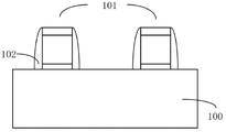
首先,如图1A所示,提供半导体衬底100,在所述半导体衬底100上形成有栅极结构101,作为一个示例,所述栅极结构101可包括自下而上依次层叠的栅极介电层、栅极材料层和栅极硬掩蔽层。此外,作为示例,在所述半导体衬底100上还形成有位于所述栅极结构101两侧且紧靠所述栅极结构101的侧壁结构102。接下来,对所述栅极结构101两侧的半导体衬底100将要形成源/漏区的区域实施离子注入,以形成LDD结构。First, as shown in FIG. 1A, a
接着,如图1B所示,在所述栅极结构101两侧形成紧靠所述侧壁结构102的间隙壁结构103,以形成用于蚀刻硅凹槽的窗口。接下来,通过所述窗口,在所述半导体衬底100中形成∑状凹槽104,通常采用先干法蚀刻再湿法蚀刻的工艺形成所述∑状凹槽104。Next, as shown in FIG. 1B ,
最后,如图1C所示,采用选择性外延生长工艺在所述∑状凹槽104中形成嵌入式锗硅105。Finally, as shown in FIG. 1C , embedded
由于半导体器件的尺寸不断缩小,实施嵌入式锗硅工艺的工艺窗口也随之不断缩小,因此,通过形成具有更宽更深尺寸的嵌入式锗硅来增强作用于PMOS沟道区的应力变得十分困难。As the size of semiconductor devices continues to shrink, the process window for implementing the embedded SiGe process is also shrinking. Therefore, it becomes very important to enhance the stress acting on the PMOS channel region by forming embedded SiGe with wider and deeper dimensions. difficulty.
因此,需要提出一种方法,在现有的工艺条件下,可以通过嵌入式锗硅进一步增强作用于PMOS沟道区的应力。Therefore, it is necessary to propose a method, under the existing process conditions, the stress acting on the PMOS channel region can be further enhanced by embedded silicon germanium.
发明内容 Contents of the invention
针对现有技术的不足,本发明提供一种半导体器件的制造方法,包括:提供半导体衬底,所述半导体衬底上形成有栅极结构,且所述栅极结构两侧形成有紧靠所述栅极结构的侧壁结构;在所述栅极结构之间的半导体衬底中形成硅凹槽;蚀刻所述硅凹槽,以形成第一∑状凹槽;在所述第一∑状凹槽中形成第一锗硅层;形成覆盖所述栅极结构的间隙壁结构;在所述栅极结构之间的半导体衬底中形成第二∑状凹槽;在所述第二∑状凹槽中形成第二锗硅层。Aiming at the deficiencies of the prior art, the present invention provides a method for manufacturing a semiconductor device, comprising: providing a semiconductor substrate, a gate structure is formed on the semiconductor substrate, and two sides of the gate structure are formed close to the gate structure. The sidewall structure of the gate structure; silicon grooves are formed in the semiconductor substrate between the gate structures; the silicon grooves are etched to form a first Σ-shaped groove; forming a first silicon germanium layer in the groove; forming a spacer structure covering the gate structure; forming a second Σ-shaped groove in the semiconductor substrate between the gate structures; forming a second Σ-shaped groove in the second Σ-shaped A second silicon germanium layer is formed in the groove.
进一步,通过所述侧壁结构构成的工艺窗口来形成所述硅凹槽。Further, the silicon groove is formed through the process window formed by the sidewall structure.
进一步,采用湿法蚀刻工艺实施所述硅凹槽的蚀刻。Further, a wet etching process is used to etch the silicon groove.
进一步,所述第一∑状凹槽的深度为10-30nm。Further, the depth of the first Σ-shaped groove is 10-30 nm.
进一步,所述第一锗硅层的锗含量为5%-20%Further, the germanium content of the first silicon germanium layer is 5%-20%
进一步,在形成所述第一锗硅层之后,还包括对所述栅极结构两侧的半导体衬底中将要形成源/漏区的区域实施离子注入的步骤,以形成LDD结构。Further, after forming the first silicon germanium layer, it also includes the step of performing ion implantation on the regions of the semiconductor substrate on both sides of the gate structure where source/drain regions will be formed, so as to form an LDD structure.
进一步,通过所述间隙壁结构构成的工艺窗口,采用先干法蚀刻再湿法蚀刻的工艺来形成所述第二∑状凹槽。Further, through the process window formed by the spacer structure, the second Σ-shaped groove is formed by first dry etching and then wet etching.
进一步,所述第二∑状凹槽的深度为50-90nm。Further, the depth of the second Σ-shaped groove is 50-90 nm.
进一步,所述第二锗硅层的锗含量为15%-60%。Further, the germanium content of the second silicon germanium layer is 15%-60%.
进一步,采用外延生长工艺形成所述第一锗硅层和所述第二锗硅层。Further, the first silicon germanium layer and the second silicon germanium layer are formed by using an epitaxial growth process.
进一步,所述第一锗硅层的锗含量低于所述第二锗硅层的锗含量。Further, the germanium content of the first silicon germanium layer is lower than that of the second silicon germanium layer.
进一步,所述栅极结构包括依次层叠的栅极介电层、栅极材料层和栅极硬掩蔽层。Further, the gate structure includes a gate dielectric layer, a gate material layer and a gate hard mask layer stacked in sequence.
根据本发明,可以通过嵌入式锗硅进一步增强作用于PMOS沟道区的应力,还可以更好地控制器件栅极和漏极之间的叠加电容的大小。According to the present invention, the stress acting on the PMOS channel region can be further enhanced through the embedded silicon germanium, and the size of the overlapping capacitance between the gate and the drain of the device can also be better controlled.
附图说明 Description of drawings
本发明的下列附图在此作为本发明的一部分用于理解本发明。附图中示出了本发明的实施例及其描述,用来解释本发明的原理。The following drawings of the invention are hereby included as part of the invention for understanding the invention. The accompanying drawings illustrate embodiments of the invention and description thereof to explain principles of the invention.
附图中:In the attached picture:
图1A-图1C为现有的嵌入式锗硅工艺的实施过程的各步骤的示意性剖面图;1A-1C are schematic cross-sectional views of various steps in the implementation process of the existing embedded silicon germanium process;
图2A-图2F为本发明提出的形成双嵌入式锗硅的方法的各步骤的示意性剖面图;2A-2F are schematic cross-sectional views of each step of the method for forming dual-embedded silicon germanium proposed by the present invention;
图3为本发明提出的形成双嵌入式锗硅的方法的流程图。FIG. 3 is a flow chart of the method for forming dual-embedded SiGe proposed by the present invention.
具体实施方式 Detailed ways
在下文的描述中,给出了大量具体的细节以便提供对本发明更为彻底的理解。然而,对于本领域技术人员而言显而易见的是,本发明可以无需一个或多个这些细节而得以实施。在其他的例子中,为了避免与本发明发生混淆,对于本领域公知的一些技术特征未进行描述。In the following description, numerous specific details are given in order to provide a more thorough understanding of the present invention. It will be apparent, however, to one skilled in the art that the present invention may be practiced without one or more of these details. In other examples, some technical features known in the art are not described in order to avoid confusion with the present invention.
为了彻底理解本发明,将在下列的描述中提出详细的步骤,以便阐释本发明提出的形成双嵌入式锗硅的方法。显然,本发明的施行并不限定于半导体领域的技术人员所熟习的特殊细节。本发明的较佳实施例详细描述如下,然而除了这些详细描述外,本发明还可以具有其他实施方式。For a thorough understanding of the present invention, detailed steps will be presented in the following description to illustrate the method for forming dual damascene SiGe proposed by the present invention. Obviously, the practice of the invention is not limited to specific details familiar to those skilled in the semiconductor arts. Preferred embodiments of the present invention are described in detail below, however, the present invention may have other embodiments besides these detailed descriptions.
应当理解的是,当在本说明书中使用术语“包含”和/或“包括”时,其指明存在所述特征、整体、步骤、操作、元件和/或组件,但不排除存在或附加一个或多个其他特征、整体、步骤、操作、元件、组件和/或它们的组合。It should be understood that when the terms "comprising" and/or "comprising" are used in this specification, they indicate the presence of the features, integers, steps, operations, elements and/or components, but do not exclude the presence or addition of one or Multiple other features, integers, steps, operations, elements, components and/or combinations thereof.
下面,参照图2A-图2F和图3来描述本发明提出的形成双嵌入式锗硅的方法的详细步骤。Next, the detailed steps of the method for forming dual-embedded SiGe proposed by the present invention will be described with reference to FIG. 2A-FIG. 2F and FIG. 3 .
参照图2A-图2F,其中示出了本发明提出的形成双嵌入式锗硅的方法的各步骤的示意性剖面图。Referring to FIG. 2A-FIG. 2F , there are shown schematic cross-sectional views of each step of the method for forming dual-embedded silicon germanium proposed by the present invention.
首先,如图2A所示,提供半导体衬底200,所述半导体衬底200的构成材料可以采用未掺杂的单晶硅、掺杂有杂质的单晶硅、绝缘体上硅(SOI)等。作为示例,在本实施例中,所述半导体衬底200选用单晶硅材料构成。在所述半导体衬底200中形成有隔离结构以及各种阱(well)结构,为了简化,图示中予以省略。First, as shown in FIG. 2A , a
在所述半导体衬底200上形成有栅极结构201,作为一个示例,所述栅极结构201可包括自下而上依次层叠的栅极介电层、栅极材料层和栅极硬掩蔽层。栅极介电层可包括氧化物,如,二氧化硅(SiO2)层。栅极材料层可包括多晶硅层、金属层、导电性金属氮化物层、导电性金属氧化物层和金属硅化物层中的一种或多种,其中,金属层的构成材料可以是钨(W)、镍(Ni)或钛(Ti);导电性金属氮化物层可包括氮化钛(TiN)层;导电性金属氧化物层可包括氧化铱(IrO2)层;金属硅化物层可包括硅化钛(TiSi)层。栅极硬掩蔽层可包括氧化物层、氮化物层、氮氧化物层和无定形碳中的一种或多种,其中,氧化物层可包括硼磷硅玻璃(BPSG)、磷硅玻璃(PSG)、正硅酸乙酯(TEOS)、未掺杂硅玻璃(USG)、旋涂玻璃(SOG)、高密度等离子体(HDP)或旋涂电介质(SOD);氮化物层可包括氮化硅(Si3N4)层;氮氧化物层可包括氮氧化硅(SiON)层。A
此外,作为示例,在所述半导体衬底200上还形成有位于所述栅极结构201两侧且紧靠所述栅极结构201的侧壁结构202。本实施例中,所述侧壁结构202的构成材料为二氧化硅。In addition, as an example,
接下来,通过所述侧壁结构202构成的工艺窗口,在所述栅极结构201之间的半导体衬底200中形成硅凹槽203。形成所述硅凹槽203的工艺可以选用本领域技术人员所熟习的适合的工艺,例如,采用干法蚀刻工艺纵向蚀刻所述栅极结构201之间的半导体衬底200以形成所述硅凹槽203。Next,
接着,如图2B所示,采用湿法蚀刻工艺蚀刻所述硅凹槽203,以形成第一∑状凹槽204。在本实施例中,利用所述湿法蚀刻的蚀刻剂在所述半导体衬底200的材料的不同晶向上的蚀刻速率不同的特性(100和110晶向的蚀刻速率高于111晶向的蚀刻速率),扩展蚀刻所述硅凹槽203以形成所述第一∑状凹槽204。所述第一∑状凹槽204的深度为10-30nm。Next, as shown in FIG. 2B , the
接着,如图2C所示,采用外延生长工艺在所述第一∑状凹槽204中形成第一锗硅层205。所述外延生长工艺可以采用低压化学气相沉积(LPCVD)、等离子体增强化学气相沉积(PECVD)、超高真空化学气相沉积(UHVCVD)、快速热化学气相沉积(RTCVD)和分子束外延(MBE)中的一种。所述第一锗硅层205的锗含量为5%-20%。Next, as shown in FIG. 2C , a
接下来,对所述栅极结构201两侧的半导体衬底200中将要形成源/漏区的区域实施离子注入,以形成LDD结构。本领域技术人员可以知晓的是,所述离子注入的具体工艺参数依据设计半导体器件时期望达到的要求而定。Next, ion implantation is performed on the regions of the
接着,如图2D所示,形成覆盖所述栅极结构201的间隙壁结构206。形成所述间隙壁结构206的工艺为本领域技术人员所熟习,在此不再加以赘述。本实施例中,所述间隙壁结构206的材料为氮化硅。Next, as shown in FIG. 2D , a
接着,如图2E所示,通过所述间隙壁结构206构成的工艺窗口,在所述栅极结构201之间的半导体衬底200中形成第二∑状凹槽207。采用先干法蚀刻再湿法蚀刻的工艺形成所述第二∑状凹槽207。所述第二∑状凹槽207的深度为50-90nm。Next, as shown in FIG. 2E , through the process window formed by the
接着,如图2F所示,采用外延生长工艺在所述第二∑状凹槽207中形成第二锗硅层208。所述外延生长工艺可以采用低压化学气相沉积(LPCVD)、等离子体增强化学气相沉积(PECVD)、超高真空化学气相沉积(UHVCVD)、快速热化学气相沉积(RTCVD)和分子束外延(MBE)中的一种。所述第二锗硅层的锗含量高于所述第一锗硅层的锗含量,所述第二锗硅层208的锗含量为15%-60%。Next, as shown in FIG. 2F , a
至此,完成了根据本发明示例性实施例的方法实施的全部工艺步骤,接下来,可以通过后续工艺完成整个半导体器件的制作,所述后续工艺与传统的半导体器件加工工艺完全相同。根据本发明,通过形成双嵌入式锗硅来形成具有锗含量梯度的锗硅层,该锗硅层可以对PMOS的沟道区施加更大的应力,同时可以更好地控制PMOS的栅极和漏极之间的叠加电容的大小。So far, all the process steps implemented by the method according to the exemplary embodiment of the present invention are completed, and then, the fabrication of the entire semiconductor device can be completed through a subsequent process, which is exactly the same as the traditional semiconductor device processing process. According to the present invention, a silicon germanium layer with a germanium content gradient is formed by forming double embedded silicon germanium, the silicon germanium layer can exert greater stress on the channel region of the PMOS, and at the same time can better control the gate and the gate of the PMOS. The size of the superposition capacitance between the drains.
参照图3,其中示出了本发明提出的形成双嵌入式锗硅的方法的流程图,用于简要示出整个制造工艺的流程。Referring to FIG. 3 , it shows a flow chart of the method for forming dual-embedded silicon germanium proposed by the present invention, which is used to briefly show the flow of the entire manufacturing process.
在步骤301中,提供半导体衬底,所述半导体衬底上形成有栅极结构,且所述栅极结构两侧形成有紧靠所述栅极结构的侧壁结构;In
在步骤302中,在所述栅极结构之间的半导体衬底中形成硅凹槽;In
在步骤303中,蚀刻所述硅凹槽,以形成第一∑状凹槽;In
在步骤304中,在所述第一∑状凹槽中形成第一锗硅层;In
在步骤305中,形成覆盖所述栅极结构的间隙壁结构;In
在步骤306中,在所述栅极结构之间的半导体衬底中形成第二∑状凹槽;In
在步骤307中,在所述第二∑状凹槽中形成第二锗硅层。In
本发明已经通过上述实施例进行了说明,但应当理解的是,上述实施例只是用于举例和说明的目的,而非意在将本发明限制于所描述的实施例范围内。此外本领域技术人员可以理解的是,本发明并不局限于上述实施例,根据本发明的教导还可以做出更多种的变型和修改,这些变型和修改均落在本发明所要求保护的范围以内。本发明的保护范围由附属的权利要求书及其等效范围所界定。The present invention has been described through the above-mentioned embodiments, but it should be understood that the above-mentioned embodiments are only for the purpose of illustration and description, and are not intended to limit the present invention to the scope of the described embodiments. In addition, those skilled in the art can understand that the present invention is not limited to the above-mentioned embodiments, and more variations and modifications can be made according to the teachings of the present invention, and these variations and modifications all fall within the claimed scope of the present invention. within the range. The protection scope of the present invention is defined by the appended claims and their equivalent scope.
Claims (12)
Priority Applications (1)
| Application Number | Priority Date | Filing Date | Title |
|---|---|---|---|
| CN201210261969.5A CN103578994B (en) | 2012-07-26 | 2012-07-26 | A kind of manufacture method of semiconductor device |
Applications Claiming Priority (1)
| Application Number | Priority Date | Filing Date | Title |
|---|---|---|---|
| CN201210261969.5A CN103578994B (en) | 2012-07-26 | 2012-07-26 | A kind of manufacture method of semiconductor device |
Publications (2)
| Publication Number | Publication Date |
|---|---|
| CN103578994A true CN103578994A (en) | 2014-02-12 |
| CN103578994B CN103578994B (en) | 2016-04-06 |
Family
ID=50050503
Family Applications (1)
| Application Number | Title | Priority Date | Filing Date |
|---|---|---|---|
| CN201210261969.5A Active CN103578994B (en) | 2012-07-26 | 2012-07-26 | A kind of manufacture method of semiconductor device |
Country Status (1)
| Country | Link |
|---|---|
| CN (1) | CN103578994B (en) |
Cited By (2)
| Publication number | Priority date | Publication date | Assignee | Title |
|---|---|---|---|---|
| CN103594338A (en) * | 2012-08-16 | 2014-02-19 | 中芯国际集成电路制造(上海)有限公司 | Manufacturing method for semiconductor device |
| CN103594338B (en) * | 2012-08-16 | 2016-11-30 | 中芯国际集成电路制造(上海)有限公司 | A kind of manufacture method of semiconductor device |
Citations (5)
| Publication number | Priority date | Publication date | Assignee | Title |
|---|---|---|---|---|
| TW200814319A (en) * | 2006-09-15 | 2008-03-16 | Taiwan Semiconductor Mfg | Semiconductor structure, metal oxide semiconductor device and method for forming semiconductor structure |
| US7429775B1 (en) * | 2005-03-31 | 2008-09-30 | Xilinx, Inc. | Method of fabricating strain-silicon CMOS |
| CN101335207A (en) * | 2007-06-26 | 2008-12-31 | 海力士半导体有限公司 | Semiconductor device and manufacturing method thereof |
| CN102403229A (en) * | 2010-09-17 | 2012-04-04 | 中芯国际集成电路制造(上海)有限公司 | Manufacturing method of step-shaped silicon-germanium source/drain structure |
| CN102437184A (en) * | 2010-09-29 | 2012-05-02 | 联华电子股份有限公司 | semiconductor structure |
-
2012
- 2012-07-26 CN CN201210261969.5A patent/CN103578994B/en active Active
Patent Citations (5)
| Publication number | Priority date | Publication date | Assignee | Title |
|---|---|---|---|---|
| US7429775B1 (en) * | 2005-03-31 | 2008-09-30 | Xilinx, Inc. | Method of fabricating strain-silicon CMOS |
| TW200814319A (en) * | 2006-09-15 | 2008-03-16 | Taiwan Semiconductor Mfg | Semiconductor structure, metal oxide semiconductor device and method for forming semiconductor structure |
| CN101335207A (en) * | 2007-06-26 | 2008-12-31 | 海力士半导体有限公司 | Semiconductor device and manufacturing method thereof |
| CN102403229A (en) * | 2010-09-17 | 2012-04-04 | 中芯国际集成电路制造(上海)有限公司 | Manufacturing method of step-shaped silicon-germanium source/drain structure |
| CN102437184A (en) * | 2010-09-29 | 2012-05-02 | 联华电子股份有限公司 | semiconductor structure |
Cited By (2)
| Publication number | Priority date | Publication date | Assignee | Title |
|---|---|---|---|---|
| CN103594338A (en) * | 2012-08-16 | 2014-02-19 | 中芯国际集成电路制造(上海)有限公司 | Manufacturing method for semiconductor device |
| CN103594338B (en) * | 2012-08-16 | 2016-11-30 | 中芯国际集成电路制造(上海)有限公司 | A kind of manufacture method of semiconductor device |
Also Published As
| Publication number | Publication date |
|---|---|
| CN103578994B (en) | 2016-04-06 |
Similar Documents
| Publication | Publication Date | Title |
|---|---|---|
| CN103137624B (en) | High gate densities device and method | |
| CN104766886B (en) | FinFET and method | |
| CN104733513B (en) | It is distributed for the germanium of channel strain | |
| CN106486377B (en) | Fin type semiconductor devices and its manufacturing method | |
| CN103594370B (en) | A kind of manufacture method of semiconductor device | |
| CN104882379A (en) | FinFET device and manufacturing method thereof | |
| CN106558551B (en) | A kind of semiconductor device and its manufacturing method, electronic device | |
| CN104217952B (en) | Manufacture method of semiconductor device | |
| CN103151264B (en) | A kind of manufacture method of semiconductor devices | |
| CN104779284A (en) | FinFET device and manufacturing method thereof | |
| CN103681333B (en) | A kind of manufacture method of semiconductor devices | |
| CN103903984B (en) | A kind of manufacture method of semiconductor devices | |
| CN103794546A (en) | Method for manufacturing semiconductor device | |
| CN103578994B (en) | A kind of manufacture method of semiconductor device | |
| CN100468657C (en) | Three-dimensional multi-gate element and manufacturing method thereof | |
| CN103943501A (en) | Manufacturing method of semiconductor device | |
| CN103681263A (en) | Method for reducing stray capacitance between contact plugs and gate structure | |
| CN104051245B (en) | A kind of preparation method of semiconductor devices | |
| CN106910684A (en) | A kind of semiconductor devices and its manufacture method | |
| CN104425268A (en) | FinFET device and manufacturing method thereof | |
| CN103579334A (en) | Semiconductor device and manufacturing method thereof | |
| CN103579110B (en) | A kind of manufacture method of semiconductor device | |
| CN104022040B (en) | The manufacture method of semiconductor devices | |
| CN103545255B (en) | A kind of manufacture method of semiconductor device | |
| CN103681506B (en) | The manufacture method of a kind of semiconducter device |
Legal Events
| Date | Code | Title | Description |
|---|---|---|---|
| C06 | Publication | ||
| PB01 | Publication | ||
| SE01 | Entry into force of request for substantive examination | ||
| SE01 | Entry into force of request for substantive examination | ||
| C14 | Grant of patent or utility model | ||
| GR01 | Patent grant |