CN103209922A - Through silicon via with reduced shunt capacitance - Google Patents
Through silicon via with reduced shunt capacitance Download PDFInfo
- Publication number
- CN103209922A CN103209922A CN2011800539261A CN201180053926A CN103209922A CN 103209922 A CN103209922 A CN 103209922A CN 2011800539261 A CN2011800539261 A CN 2011800539261A CN 201180053926 A CN201180053926 A CN 201180053926A CN 103209922 A CN103209922 A CN 103209922A
- Authority
- CN
- China
- Prior art keywords
- layer
- vertical
- dielectric
- trench
- polysilicon
- Prior art date
- Legal status (The legal status is an assumption and is not a legal conclusion. Google has not performed a legal analysis and makes no representation as to the accuracy of the status listed.)
- Granted
Links
Images


Classifications
-
- B—PERFORMING OPERATIONS; TRANSPORTING
- B81—MICROSTRUCTURAL TECHNOLOGY
- B81C—PROCESSES OR APPARATUS SPECIALLY ADAPTED FOR THE MANUFACTURE OR TREATMENT OF MICROSTRUCTURAL DEVICES OR SYSTEMS
- B81C1/00—Manufacture or treatment of devices or systems in or on a substrate
-
- B—PERFORMING OPERATIONS; TRANSPORTING
- B81—MICROSTRUCTURAL TECHNOLOGY
- B81B—MICROSTRUCTURAL DEVICES OR SYSTEMS, e.g. MICROMECHANICAL DEVICES
- B81B3/00—Devices comprising flexible or deformable elements, e.g. comprising elastic tongues or membranes
- B81B3/0064—Constitution or structural means for improving or controlling the physical properties of a device
- B81B3/0086—Electrical characteristics, e.g. reducing driving voltage, improving resistance to peak voltage
-
- B—PERFORMING OPERATIONS; TRANSPORTING
- B81—MICROSTRUCTURAL TECHNOLOGY
- B81B—MICROSTRUCTURAL DEVICES OR SYSTEMS, e.g. MICROMECHANICAL DEVICES
- B81B1/00—Devices without movable or flexible elements, e.g. microcapillary devices
-
- B—PERFORMING OPERATIONS; TRANSPORTING
- B81—MICROSTRUCTURAL TECHNOLOGY
- B81B—MICROSTRUCTURAL DEVICES OR SYSTEMS, e.g. MICROMECHANICAL DEVICES
- B81B7/00—Microstructural systems; Auxiliary parts of microstructural devices or systems
- B81B7/0032—Packages or encapsulation
- B81B7/007—Interconnections between the MEMS and external electrical signals
-
- B—PERFORMING OPERATIONS; TRANSPORTING
- B81—MICROSTRUCTURAL TECHNOLOGY
- B81B—MICROSTRUCTURAL DEVICES OR SYSTEMS, e.g. MICROMECHANICAL DEVICES
- B81B7/00—Microstructural systems; Auxiliary parts of microstructural devices or systems
- B81B7/02—Microstructural systems; Auxiliary parts of microstructural devices or systems containing distinct electrical or optical devices of particular relevance for their function, e.g. microelectro-mechanical systems [MEMS]
-
- H—ELECTRICITY
- H01—ELECTRIC ELEMENTS
- H01G—CAPACITORS; CAPACITORS, RECTIFIERS, DETECTORS, SWITCHING DEVICES, LIGHT-SENSITIVE OR TEMPERATURE-SENSITIVE DEVICES OF THE ELECTROLYTIC TYPE
- H01G7/00—Capacitors in which the capacitance is varied by non-mechanical means; Processes of their manufacture
- H01G7/06—Capacitors in which the capacitance is varied by non-mechanical means; Processes of their manufacture having a dielectric selected for the variation of its permittivity with applied voltage, i.e. ferroelectric capacitors
-
- B—PERFORMING OPERATIONS; TRANSPORTING
- B81—MICROSTRUCTURAL TECHNOLOGY
- B81B—MICROSTRUCTURAL DEVICES OR SYSTEMS, e.g. MICROMECHANICAL DEVICES
- B81B2201/00—Specific applications of microelectromechanical systems
- B81B2201/02—Sensors
- B81B2201/0228—Inertial sensors
- B81B2201/0235—Accelerometers
-
- B—PERFORMING OPERATIONS; TRANSPORTING
- B81—MICROSTRUCTURAL TECHNOLOGY
- B81B—MICROSTRUCTURAL DEVICES OR SYSTEMS, e.g. MICROMECHANICAL DEVICES
- B81B2207/00—Microstructural systems or auxiliary parts thereof
- B81B2207/09—Packages
- B81B2207/091—Arrangements for connecting external electrical signals to mechanical structures inside the package
- B81B2207/094—Feed-through, via
- B81B2207/096—Feed-through, via through the substrate
Landscapes
- Engineering & Computer Science (AREA)
- Microelectronics & Electronic Packaging (AREA)
- Power Engineering (AREA)
- Computer Hardware Design (AREA)
- Manufacturing & Machinery (AREA)
- Pressure Sensors (AREA)
- Micromachines (AREA)
- Solid State Image Pick-Up Elements (AREA)
- Semiconductor Integrated Circuits (AREA)
Abstract
本文涉及用于微机电系统(MEMS)传感器的器件层的装置和方法,所述MEMS传感器具有通孔,所述通孔具有减小的并联电容。在一个实例中,器件层可包括衬底,该衬底具有在水平方向上被所述衬底的一部分分隔开的一对沟槽,其中,该对沟槽中的每个沟槽包括包含电介质的第一垂直层和第二垂直层,所述第一垂直层和第二垂直层被包含多晶硅的第三垂直层分隔开。
This document relates to apparatus and methods for a device layer for a microelectromechanical system (MEMS) sensor having a via having reduced parallel capacitance. In one example, the device layer may include a substrate having a pair of trenches horizontally separated by a portion of the substrate, wherein each of the pair of trenches includes a first vertical layer and a second vertical layer comprising a dielectric, the first and second vertical layers being separated by a third vertical layer comprising polysilicon.
Description
要求优先权claim priority
本申请要求2010年9月20日递交的、题为“TSV WITH REDUCED SHUNTCAPACITANCE(具有减小的并联电容的TSV)”(代理机构案号2921.103PRV)美国临时专利申请序列号No.61/384,319的优先权,其全部内容通过引用并入本文。This application claims U.S. Provisional Patent Application Serial No. 61/384,319, filed September 20, 2010, entitled "TSV WITH REDUCED SHUNTCAPACITANCE" (Attorney Docket No. 2921.103PRV) Priority, the entire contents of which are incorporated herein by reference.
背景技术Background technique
微机电系统(MEMS)芯片可包括多层,这多层中包括通孔层。通孔层可包括介电沟槽(trench),该介电沟槽用于形成对MEMS芯片中MEMS器件的特性进行感应的电极。这种沟槽在美国专利No.7,539,003中提及。介电沟槽可具有巨大的并联电容,该并联电容会降低MEMS器件(如用于电容传感或射频(RF)应用的MEMS器件)的性能。Micro-electro-mechanical systems (MEMS) chips may include multiple layers including via layers. The via layer may include dielectric trenches for forming electrodes for sensing characteristics of MEMS devices in the MEMS chip. Such grooves are mentioned in US Patent No. 7,539,003. Dielectric trenches can have substantial shunt capacitance that degrades the performance of MEMS devices, such as those used in capacitive sensing or radio frequency (RF) applications.
发明内容Contents of the invention
在某些实例中,微电子机械系统(MEMS)传感器可包括具有减小的并联电容的通孔(via)。在一个实例中,器件层可包括:衬底(substrate),该衬底具有在水平方向上被所述衬底的一部分分隔开的一对沟槽,其中,该对沟槽中的每个沟槽包括含电介质的第一垂直层和第二垂直层,所述第一垂直层和第二垂直层被包含多晶硅的第三垂直层分隔开。In some examples, microelectromechanical system (MEMS) sensors may include vias with reduced shunt capacitance. In one example, the device layer may include: a substrate having a pair of trenches separated by a portion of the substrate in the horizontal direction, wherein each of the pair of trenches The trench includes first and second vertical layers comprising a dielectric separated by a third vertical layer comprising polysilicon.
该部分旨在提供对本专利申请的主题的概述,而非旨在提供对本发明的排他性或穷尽性解释。本文包含了具体实施方式以提供与本专利申请有关的进一步信息。This section is intended to provide an overview of the subject matter of this patent application and is not intended to provide an exclusive or exhaustive explanation of the invention. The Detailed Description is included herein to provide further information pertaining to this patent application.
附图说明Description of drawings
在附图(其不一定按比例绘制)中,相似的附图标记可在不同的视图中描述相似的部件。具有不同字母后缀的相似附图标记可表示同类部件的不同例子。附图以示例而非限制的方式大体示出了本文中所论述的各个实例。In the drawings (which are not necessarily drawn to scale), like reference numerals may describe like parts in different views. Similar reference numbers with different letter suffixes may indicate different instances of the same component. The drawings generally illustrate various examples discussed herein, by way of illustration and not limitation.
图1大体示出了一个实例MEMS器件的截面图;Figure 1 generally shows a cross-sectional view of an example MEMS device;
图2大体示出了一个实例通孔层的布局视图;Figure 2 generally shows a layout view of an example via layer;
图3A大体示出了通孔层的一个实例TSV结构的等效电路300;FIG. 3A generally shows an equivalent circuit 300 of an example TSV structure of a via layer;
图3B大体示出了通孔层的一个实例TSV结构的可选的布局等效电路;FIG. 3B generally shows an alternative layout equivalent circuit of an example TSV structure of a via layer;
图4大体示出了作为不同沟槽结构和感应电容的频率函数的阻抗的比较;Figure 4 generally shows a comparison of impedance as a function of frequency for different trench structures and inductive capacitances;
图5大体示出了对于四种沟槽结构感应电容器阻抗与并联阻抗作为频率的函数的比较。Figure 5 generally shows a comparison of sense capacitor impedance and shunt impedance as a function of frequency for four trench structures.
具体实施方式Detailed ways
发明人已经发现用于在MEMS器件的通孔层中形成电极的结构和方法,其明显减小了与现有设计相关的并联电容。在某些实例中,集成MEMS器件的一层可包括多个高电阻率的多晶填充层(poly filled layer)与多个电介质层(dielectic layer)相互交错的硅通孔(TSV)结构。所述TSV结构能够将高电阻率多晶与电介质串联连接,由此减小对所述MEMS器件中感应电容器的电容分流效应(capacitive shunting effect)。在某些实例中,与所述MEMS器件相关的电子器件的工作频率可选择为使得所述感应电容器的阻抗大于并联电容的阻抗,由此减小所述并联电容的影响。在一个实例中,包括低K电介质或包括低K电介质与其他材料(如热氧化物、掺杂氧化物或其他介电材料)的组合的介电沟槽可降低并联电容,例如,所述低K电介质的介电常数小于用在沟槽中的氧化物的介电常数。在一个实例中,所述低K电介质的介电常数可约为氧化物的介电常数的一半。The inventors have discovered structures and methods for forming electrodes in the via layer of MEMS devices that significantly reduce the parallel capacitance associated with prior designs. In some examples, one layer of the integrated MEMS device may include a through-silicon via (TSV) structure in which multiple high-resistivity poly filled layers (poly filled layers) and multiple dielectric layers (dielectric layers) are interleaved. The TSV structure enables the series connection of high-resistivity polys with a dielectric, thereby reducing capacitive shunting effects on sensing capacitors in the MEMS device. In some examples, the operating frequency of the electronics associated with the MEMS device may be selected such that the impedance of the sensing capacitor is greater than the impedance of the parallel capacitance, thereby reducing the effect of the parallel capacitance. In one example, dielectric trenches comprising low-K dielectrics or combinations of low-K dielectrics with other materials such as thermal oxides, doped oxides, or other dielectric materials can reduce shunt capacitance, e.g., the low The K dielectric has a lower dielectric constant than the oxide used in the trench. In one example, the dielectric constant of the low-K dielectric can be about half that of the oxide.
在某些实例中,沟槽可部分地由多晶填充且处于负压下(如真空中)。处于真空中的沟槽区域内的介电常数可以是氧化物的介电常数的1/4,由此减小由氧化物填充的沟槽的并联电容。In some examples, the trenches may be partially filled with polycrystalline and under negative pressure (eg, vacuum). The dielectric constant within the trench region in vacuum may be 1/4 that of the oxide, thereby reducing the parallel capacitance of the oxide-filled trench.
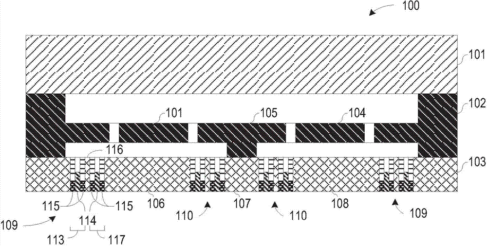
图1大体示出了一个实例MEMS器件100的截面图。在某些实例中,MEMS器件100可包括三层:覆盖层(cap layer)101、器件层102和通孔层103。器件层102可包括由锚105支撑的可移动部分104。在某些实例中,MEMS器件100的可移动部分104可由硅晶圆刻蚀而成。经刻蚀的器件层102可包括允许对可移动部分104的平面内(in-plane)和平面外(out-ofplane)移动进行感应的结构。在某些实例中,可移动部分104可被驱动为以特定频率进行振荡,从而允许对MEMS器件100的角加速度进行感应。FIG. 1 generally illustrates a cross-sectional view of an
覆盖层101可提供器件层102中可移动部分104的环境外壳(environmentalenclosure)的至少一部分。在某些实例中,覆盖层101可包括凹部(未示出)以适应器件层102中的可移动部分104的移动。在一个实例中,覆盖层101可限制例如在MEMS器件100机械震动时,器件层102的可移动部分104的移动。在某些实例中,覆盖层101与器件层102相粘合,从而可使器件层102的可移动部分104周围保持真空。Cover layer 101 may provide at least a portion of an environmental enclosure for
通孔层103也可提供器件层102中可移动部分104的环境外壳的至少一部分。在某些实例中,通孔层103可包括用于感应或驱动器件层102中的可移动部分104的电极106、107、108。在一个实例中,器件层电极中的一个或多个电极,例如驱动电极107,可为器件层102提供驱动信号。在一个实例中,通孔层103中的一个或多个感应电极106、108可提供对器件层102中的可移动部分104的移动进行指示的感应信息。在某些实例中,感应信息可包括与器件层102中的可移动部分104的移动相关的感应电容的变化。在一个实例中,通孔层103内的沟槽109、110可为所述感应电极提供一定程度的电隔离。Via
图2大体示出了包括与现有结构相比可提供减小的并联电容的沟槽或通孔结构的实例通孔层203的布局视图。通孔层203的布局包括用于多个电极的区域。在一个实例中,通孔层203的布局可包括位于中心附近的驱动电极207和围绕驱动电极207的感应电极206、208。在某些实例中,所述感应电极可通过介电沟槽或通孔结构209、210与驱动电极207以及通孔层203的硅的外部区域隔离。2 generally illustrates a layout view of an example via
参见图1,可延展至图2的实例,在一个实例中,介电沟槽109、110可包括第一沟槽区域113,该第一沟槽区域113包括位于垂直介电层115之间的垂直多晶硅层114。在一个实例中,第二沟槽区域117可包括位于介电层115之间的第二垂直多晶硅层118,其中,第二沟槽区域117通过垂直单晶硅层116与所述第一沟槽区域隔离。关于图1,驱动信号可经由通孔层103的部分(如,通过四重介电沟槽110与感应电极106、108电隔离的锚电极107)施加至器件层102中的可移动部分104。在一个实例中,感应电极106、108中除与驱动电极107相对的一侧之外的另一侧可通过另一四重介电沟槽109与通孔层103的接地部分隔离。Referring to FIG. 1 , extending to the example of FIG. 2 , in one example, the
在一个实例中,未示出地,一隔离沟槽可将感应电极包围,且一单独的沟槽可形成于所述锚电极的周围以连接驱动电压。由于所述驱动电压不易受并联电容的影响,因此简单的单个沟槽即可用于隔离所述锚电极。In one example, not shown, an isolation trench can surround the sensing electrode, and a separate trench can be formed around the anchor electrode to connect the driving voltage. Since the drive voltage is not susceptible to shunt capacitance, a simple single trench can be used to isolate the anchor electrodes.
所述MEMS器件的传感器可包括连接到感应电极106、108的感应电容。器件层102中可移动部分104的移动可改变所述感应电容。某些实例中的包含低阻单晶硅的感应电极106、108可用于测量所述感应电容的变化。The sensor of the MEMS device may include a sensing capacitor connected to the
图3A大体示出了通孔层的一个实例TSV结构的等效电路300。在某些实例中,所述等效电路可包括驱动电极307、感应电极306、感应电容326、第一TSV网络310和第二TSV网络309。感应电容326可随所述器件层的移动而改变。在一个实例中,第一TSV网络310可表示驱动电极307与感应电极306之间的隔离沟槽。第二TSV网络309可表示感应电极306与所述通孔层的周界部分之间的隔离沟槽。每个网络309、310可包括四个电容元件315和三个电阻元件314、316。电容元件315可与如上结合图1和图2论述的四个垂直介电层相关。三个电阻元件中的两个电阻元件314可与两个垂直多晶硅层相关。在一个实例中,第三电阻元件316可与低阻的垂直单晶硅层相关。相对高阻的垂直多晶硅层314与电介质的并联电容315串联连接,可减小对所述传感器的分流效应,从而改善感应电容326的性能。FIG. 3A generally illustrates an equivalent circuit 300 of an example TSV structure for a via layer. In some examples, the equivalent circuit may include a driving
图3B大体示出了通孔层的一个实例TSV结构的替代的布局等效电路。例如,由于低源阻抗,所述驱动电压大体上不易受并联电容的影响,因此会出现由在感应电容器输出处的加载引起的MEMS传感器性能的劣化。在使用该替代布局的实例中,等效电路330示出了TSV结构331、332的并联电容加载在感应电容326的两侧。FIG. 3B generally shows an alternative layout equivalent circuit of an example TSV structure of the via layer. For example, due to the low source impedance, the drive voltage is generally less susceptible to shunt capacitance, thus degrading MEMS sensor performance due to loading at the sense capacitor output. In an example using this alternative layout, the
对减小并联电容的其他改进可通过使用多晶硅和电介质的不同组合与类型来实现。例如,当垂直介电层包括两种材料时,例如包括介电常数约为3.9以确保密封性(hermeticity)的热氧化物和介电常数约为2以在制作过程期间提供结构强度的低K电介质时,可进一步减小并联电容。在某些实例中,低K介电材料可为多孔的,由此无法保持真空。因此,一些低K电介质不适于100%沟槽填充。组合介电层可保持真空并具备与低K电介质相关的好处。Other improvements to reducing shunt capacitance can be achieved by using different combinations and types of polysilicon and dielectric. For example, when the vertical dielectric layer includes two materials, such as a thermal oxide with a dielectric constant of about 3.9 to ensure hermeticity and a low K with a dielectric constant of about 2 to provide structural strength during the fabrication process. When the dielectric is used, the parallel capacitance can be further reduced. In some examples, low-K dielectric materials may be porous and thus unable to hold a vacuum. Therefore, some low-k dielectrics are not suitable for 100% trench fill. The combined dielectric layer maintains the vacuum and has the benefits associated with low-K dielectrics.
在一个实例中,并联电容的减小X作为沟槽长度和分别为K1、K2的各介电常数的函数,可取决于氧化物含量(O%)和低K电介质含量(D%)。例如,In one example, the reduction X of the shunt capacitance as a function of the trench length and the respective dielectric constants of K1, K2, respectively, may depend on the oxide content (O%) and the low-K dielectric content (D%). For example,
X=(K2*D+K1*O)/K1X=(K2*D+K1*O)/K1
如果氧化物占沟槽的20%且低K电介质占80%,且K1=3.9,K2=2,那么,If oxide occupies 20% of the trench and low-K dielectric occupies 80%, and K1=3.9, K2=2, then,
X=(2*0.8+3.9*0.2)/3.9=0.61,X=(2*0.8+3.9*0.2)/3.9=0.61,
表示与仅由氧化物填充的沟槽相比,并联电容减小了39%。represents a 39% reduction in shunt capacitance compared to trenches filled only with oxide.
如果沟槽长度为4.0mm,通孔层为200um,沟槽面积为0.8mm2,则对于1um厚的电介质,其氧化物电容约为27.6pF。以低K介电材料对沟槽的80%进行填充,可将电容减小至约为16.8pF。If the trench length is 4.0mm, the via layer is 200um, and the trench area is 0.8mm 2 , the oxide capacitance is about 27.6pF for a 1um thick dielectric. Filling 80% of the trench with a low-K dielectric reduces the capacitance to about 16.8pF.
对沟槽的非介电垂直层进行部分地填充也可减小并联电容。在某些实例中,如果在所述TSV的制作过程中将部分多晶硅填充物去除(刻蚀),可进一步减小并联电容。该减小效果与使用低K电介质的效果相似。当多晶硅层的厚度是介电层的几倍且所述沟槽暴露于介电常数约为1(是一些低K电介质的1/2)的真空中时,该减小效果可更大。对于上述实例的沟槽,如果约为80%的多晶硅厚度被去除,则并联电容会从约27.6pf降到约6.1pf。Partially filling the non-dielectric vertical layers of the trenches also reduces shunt capacitance. In some examples, if part of the polysilicon filling is removed (etched) during the fabrication of the TSV, the shunt capacitance can be further reduced. This reduction effect is similar to that of using a low-K dielectric. This reduction can be even greater when the polysilicon layer is several times thicker than the dielectric layer and the trenches are exposed to a vacuum with a dielectric constant of about 1 (1/2 that of some low-K dielectrics). For the trenches of the above example, if about 80% of the polysilicon thickness is removed, the shunt capacitance drops from about 27.6 pf to about 6.1 pf.
图4大体示出了作为各种沟槽结构和1pf感应电容405的阻抗-频率函数的比较。所述各种沟槽结构包括具有高阻多晶填充物的单沟槽结构401、双沟槽结构402和四重沟槽结构403,以及使用低K电介质和80%多晶硅回蚀的四重沟槽结构404。FIG. 4 generally shows a comparison of impedance as a function of frequency for various trench structures and 1
信噪比的劣化及由此产生的可用性能损失可正比于感应电容器阻抗与并联阻抗的比值。图5大体示出了(感应电容器/四种沟槽结构的并联阻抗)-频率函数的比较。四种结构包括具有高电阻率的多晶填充物的单沟槽结构501、双沟槽结构502和四重沟槽结构503,以及使用低K电介质和80%多晶硅回蚀的四重沟槽结构504。选择比值低于1的电子器件的工作频率能够使得TSV电容的分流影响大幅度减小。高阻多晶硅可提供足够低的低信噪比以避免过多的功耗。例如,比较显示,所述单沟槽结构在示出的频率范围内看不到感应电容器阻抗与并联阻抗的比值低于1。相反,具有低K电介质和20%多晶填充物的所述四重沟槽结构在直流状态下,感应电容器阻抗与并联阻抗的比值低于1,且在639kHz附近,该比值低于0.1。一般而言,MEMS器件的工作频率越低,则功耗越低,当在具有受限电源的移动系统中使用MEMS器件时,可具备显著优势。The degradation of the signal-to-noise ratio and the resulting loss of usable performance can be proportional to the ratio of the sense capacitor impedance to the shunt impedance. Figure 5 generally shows a comparison of (sensing capacitor/parallel impedance of four trench structures) versus frequency functions. The four structures include
补充注释及实例Supplementary notes and examples
在实例1中,一种方法包括:在硅衬底的第一侧刻蚀出至少一对沟槽,在所述硅衬底的第一侧上形成氧化物层,在所述氧化物层上形成多晶硅层,将在该对沟槽中的每个沟槽内的所述多晶硅层回蚀至预定深度,以及在所述沟槽的侧壁上形成介电层,所述介电层包括所述氧化物层的一部分和第二介电材料。In Example 1, a method includes: etching at least one pair of trenches on a first side of a silicon substrate, forming an oxide layer on the first side of the silicon substrate, and on the oxide layer forming a polysilicon layer, etching back the polysilicon layer in each of the pair of trenches to a predetermined depth, and forming a dielectric layer on sidewalls of the trenches, the dielectric layer comprising the part of the oxide layer and the second dielectric material.
在实例2中,实例1的所述方法可选地包括在所述氧化物层的顶部形成氮化物层。In Example 2, the method of Example 1 optionally includes forming a nitride layer on top of the oxide layer.
在实例3中,实例1至2中任意一个或多个实例的所述形成氮化物层可选地包括:将所述多晶硅层的一部分去除,直至到达所述沟槽中的氧化物层的上表面,其中,所述将所述多晶硅层的一部分去除包括:将所述多晶硅层的位于所述沟槽中的部分留下。In Example 3, the forming of the nitride layer in any one or more of Examples 1 to 2 may optionally include: removing a part of the polysilicon layer until reaching the upper surface of the oxide layer in the trench. surface, wherein the removing a part of the polysilicon layer includes: leaving a part of the polysilicon layer located in the trench.
在实例4中,实例1至3中任意一个或多个实例的在所述氧化物层的顶部形成氮化物层可选地包括:在所述氮化物层的顶部形成抗蚀层(resist 1ayer)。In Example 4, forming a nitride layer on top of the oxide layer in any one or more of Examples 1 to 3 optionally includes: forming a resist layer on top of the nitride layer .
在实例5中,实例1至4中任意一个或多个实例的所述方法可选地包括:对所述抗蚀层进行图案化以限定凹部的边界。In Example 5, the method of any one or more of Examples 1-4 optionally includes patterning the resist layer to define boundaries of recesses.
在实例6中,实例1至5中任意一个或多个实例的所述方法可选地包括:去除所述氮化物的一部分以进一步限定所述凹部的所述边界。In Example 6, the method of any one or more of Examples 1-5 optionally includes removing a portion of the nitride to further define the boundary of the recess.
在实例7中,实例1至6中任意一个或多个实例的所述方法可选地包括:刻蚀所述凹部到所述硅衬底。In Example 7, the method of any one or more of Examples 1 to 6 optionally includes: etching the recess into the silicon substrate.
在实例8中,实例1至7中任意一个或多个实例的所述刻蚀所述凹部可选地包括:从所述沟槽的侧壁上去除所述氧化物层的一部分。In Example 8, the etching the recess in any one or more of Examples 1 to 7 may optionally include: removing a part of the oxide layer from a sidewall of the trench.
在实例9中,实例1至8中任意一个或多个实例的所述形成氧化物层可选地包括:在所述沟槽的侧壁上形成氧化物层。In Example 9, the forming of an oxide layer in any one or more of Examples 1 to 8 may optionally include: forming an oxide layer on a sidewall of the trench.
在实例10中,实例1至9中任意一个或多个实例的所述方法可选地包括:将所述硅衬底的所述第一侧的一部分与MEMS传感器的器件层相粘合。In Example 10, the method of any one or more of Examples 1-9 optionally includes bonding a portion of the first side of the silicon substrate to a device layer of a MEMS sensor.
在实例11中,实例1至10中任意一个或多个实例的所述方法可选地包括:磨削所述硅衬底的第二侧以暴露所述沟槽的第一端。In Example 11, the method of any one or more of Examples 1-10 optionally includes grinding the second side of the silicon substrate to expose the first end of the trench.
在实例12中,用于MEMS器件的一种通孔层,可包括:衬底,具有在水平方向上被所述衬底的一部分分隔开的一对沟槽,其中,该对沟槽中的每个沟槽包括包含第一材料的第一垂直层和第二垂直层,所述第一垂直层和第二垂直层被包含第二材料的第三垂直层分隔开,其中,所述第一材料包括电介质。In Example 12, a via layer for a MEMS device may include: a substrate having a pair of trenches separated by a portion of the substrate in the horizontal direction, wherein the pair of trenches Each trench of comprises a first vertical layer comprising a first material and a second vertical layer separated by a third vertical layer comprising a second material, wherein the The first material includes a dielectric.
在实例13中,实例1至12中任意一个或多个实例的所述第二材料可选地包括:多晶硅。In Example 13, the second material of any one or more of Examples 1 to 12 may optionally include: polysilicon.
在实例14中,实例1至13中任意一个或多个实例的所述第三垂直层可选地包括:包含少于80%的多晶硅的量。In Example 14, the third vertical layer of any one or more of Examples 1-13 optionally includes an amount of polysilicon comprising less than 80%.
在实例15中,实例1至14中任意一个或多个实例的所述第三垂直层可选地包括:包含少于20%的多晶硅的量。In Example 15, the third vertical layer of any one or more of Examples 1-14 optionally includes an amount of polysilicon comprising less than 20%.
在实例16中,实例1至16中任意一个或多个实例的所述第一垂直层和第二垂直层可选地包括:热氧化物。In Example 16, the first vertical layer and the second vertical layer of any one or more of Examples 1-16 optionally include: thermal oxide.
在实例17中,实例1至16中任意一个或多个实例的所述第一垂直层和第二垂直层的每一层可选地包括:热氧化物和第三材料,所述第三材料的介电常数小于所述热氧化物的介电常数。In Example 17, each of the first vertical layer and the second vertical layer of any one or more of Examples 1 to 16 optionally includes: a thermal oxide and a third material, the third material The dielectric constant is less than that of the thermal oxide.
在实例18中,实例1至17中任意一个或多个实例的所述第一材料可选地包括:热氧化物,且实例17中的所述第二材料可选地包括:电介质,所述电介质的介电常数小于所述热氧化物的介电常数。In Example 18, the first material of any one or more of Examples 1 to 17 optionally includes: a thermal oxide, and the second material in Example 17 optionally includes: a dielectric, the The dielectric constant of the dielectric is less than that of the thermal oxide.
在实例19中,一种传感器可包括:覆盖层、连接到所述覆盖层的器件层(包括检测质量块)和连接到所述器件层的通孔层,其中,所述器件层可包括:硅衬底,具有在水平方向上被所述硅衬底的一部分分隔开的一对沟槽,且其中,该对沟槽中的每个沟槽包括含电介质的第一垂直层和第二垂直层,所述第一垂直层和第二垂直层被包含多晶硅的第三垂直层分隔开。In Example 19, a sensor can include: a cover layer, a device layer (including a proof mass) connected to the cover layer, and a via layer connected to the device layer, wherein the device layer can include: A silicon substrate having a pair of trenches separated horizontally by a portion of the silicon substrate, and wherein each trench of the pair of trenches includes a first vertical layer comprising a dielectric and a second vertical layers, the first vertical layer and the second vertical layer are separated by a third vertical layer comprising polysilicon.
在实例20中,实例1至19中任意一个或多个实例的所述第三垂直层可选地包括:少于80%的多晶硅的量。In Example 20, the third vertical layer of any one or more of Examples 1-19 optionally includes an amount of polysilicon that is less than 80%.
在实例21中,实例1至20中任意一个或多个实例的所述第三垂直层可选地包括:少于20%的多晶硅的量。In Example 21, the third vertical layer of any one or more of Examples 1-20 optionally includes an amount of polysilicon that is less than 20%.
在实例22中,实例1至21中任意一个或多个实例的所述第一垂直层和第二垂直层可选地包括:热氧化物。In Example 22, the first vertical layer and the second vertical layer of any one or more of Examples 1-21 optionally include: thermal oxide.
在实例23中,实例1至22中任意一个或多个实例的所述第一垂直层和第二垂直层的每一层可选地包括:热氧化物和第二材料,所述第二材料的介电常数小于所述热氧化物的介电常数。In Example 23, each of the first vertical layer and the second vertical layer of any one or more of Examples 1 to 22 optionally includes: a thermal oxide and a second material, the second material The dielectric constant is less than that of the thermal oxide.
上述详细说明书参照了附图,附图也是所述详细说明书的一部分。附图以图解的方式显示了可应用本发明的具体实施例。这些实施例在本发明中被称作“示例”。本发明所涉及的所有出版物、专利及专利文件全部作为本发明的参考内容,尽管它们是分别加以参考的。如果本发明与参考文件之间存在用途差异,则将参考文件的用途视作本发明的用途的补充,若两者之间存在不可调和的差异,则以本发明的用途为准。The above detailed description refers to the accompanying drawings, which form a part hereof. The drawings show by way of diagrams specific embodiments to which the invention may be applied. These embodiments are referred to as "examples" in the present invention. All publications, patents, and patent documents referred to in this application are hereby incorporated by reference in their entirety, although individually incorporated by reference. If there is a difference in use between the present invention and the reference document, the use of the reference document is regarded as a supplement to the use of the present invention, and if there is an irreconcilable difference between the two, the use of the present invention shall prevail.
在本发明中,与专利文件通常使用的一样,术语“一”或“某一”表示包括一个或多个,但其他情况或在使用“至少一个”或“一个或多个”时应除外。在本发明中,除非另外指明,否则使用术语“或”指无排他性的或者,使得“A或B”包括:“A但不是B”、“B但不是A”以及“A和B”。在所附权利要求中,术语“包含”和“在其中”等同于各个术语“包括”和“其中”的通俗英语。同样,在下面的权利要求中,术语“包含”和“包括”是开放性的,即,系统、装置、物品或步骤包括除了权利要求中这种术语之后所列出的那些元件以外的部件的,依然视为落在该条权利要求的范围之内。而且,在下面的权利要求中,术语“第一”、“第二”和“第三”等仅仅用作标签,并非对对象有数量要求。In the present invention, as commonly used in patent documents, the term "a" or "a" means to include one or more, but should be excluded in other cases or when "at least one" or "one or more" is used. In the present invention, unless otherwise indicated, the term "or" is used to mean a non-exclusive alternative such that "A or B" includes: "A but not B", "B but not A" and "A and B". In the appended claims, the terms "comprising" and "in which" are equivalent to the plain English equivalents of the respective terms "comprising" and "in which". Likewise, in the following claims, the terms "comprises" and "comprising" are open-ended, i.e., the system, means, article or steps include elements other than those listed after such term in the claims. , is still deemed to fall within the scope of the claim. Moreover, in the following claims, the terms "first", "second", and "third", etc. are merely used as labels and do not place quantitative requirements on the objects.
上述说明的作用在于解说而非限制。在其它示例中,上述示例(或示例的一个或多个方面)可结合使用。可以在理解上述说明书的基础上,利用现有技术的某种常规技术来执行其他实施例。遵照37C.F.R.§1.72(b)的规定提供摘要,允许读者快速确定本技术公开的性质。提交本摘要时要理解的是该摘要不用于解释或限制权利要求的范围或意义。同样,在上面的具体实施方式中,各种特征可归类成将本公开合理化。这不应理解成未要求的公开特征对任何权利要求必不可少。相反,本发明的主题可在于的特征少于特定公开的实施例的所有特征。因此,下面的权利要求据此并入具体实施方式中,每个权利要求均作为一个单独的实施例。应参看所附的权利要求,以及这些权利要求所享有的等同物的所有范围,来确定本发明的范围。The foregoing description is by way of illustration and not limitation. In other examples, the above examples (or one or more aspects of the examples) may be used in combination. Other embodiments may be implemented using certain conventional techniques of the prior art on the basis of understanding the above description. The Abstract is provided in compliance with 37 C.F.R. §1.72(b) to allow the reader to quickly ascertain the nature of the technical disclosure. This abstract is submitted with the understanding that it will not be used to interpret or limit the scope or meaning of the claims. Also, in the above Detailed Description, various features may be grouped to rationalize the disclosure. This should not be interpreted as indicating that an unclaimed disclosed feature is essential to any claim. Rather, inventive subject matter may lie in less than all features of a particular disclosed embodiment. Thus the following claims are hereby incorporated into the Detailed Description, with each claim standing as a separate embodiment. The scope of the invention should be determined with reference to the appended claims, along with the full range of equivalents to which such claims are entitled.
Claims (10)
Applications Claiming Priority (3)
| Application Number | Priority Date | Filing Date | Title |
|---|---|---|---|
| US38431910P | 2010-09-20 | 2010-09-20 | |
| US61/384,319 | 2010-09-20 | ||
| PCT/US2011/052417 WO2012040245A2 (en) | 2010-09-20 | 2011-09-20 | Through silicon via with reduced shunt capacitance |
Publications (2)
| Publication Number | Publication Date |
|---|---|
| CN103209922A true CN103209922A (en) | 2013-07-17 |
| CN103209922B CN103209922B (en) | 2014-09-17 |
Family
ID=45874333
Family Applications (1)
| Application Number | Title | Priority Date | Filing Date |
|---|---|---|---|
| CN201180053926.1A Active CN103209922B (en) | 2010-09-20 | 2011-09-20 | Through silicon via with reduced shunt capacitance |
Country Status (5)
| Country | Link |
|---|---|
| US (1) | US9006846B2 (en) |
| EP (1) | EP2619130A4 (en) |
| KR (1) | KR101311966B1 (en) |
| CN (1) | CN103209922B (en) |
| WO (1) | WO2012040245A2 (en) |
Cited By (22)
| Publication number | Priority date | Publication date | Assignee | Title |
|---|---|---|---|---|
| US8710599B2 (en) | 2009-08-04 | 2014-04-29 | Fairchild Semiconductor Corporation | Micromachined devices and fabricating the same |
| US8742964B2 (en) | 2012-04-04 | 2014-06-03 | Fairchild Semiconductor Corporation | Noise reduction method with chopping for a merged MEMS accelerometer sensor |
| US8754694B2 (en) | 2012-04-03 | 2014-06-17 | Fairchild Semiconductor Corporation | Accurate ninety-degree phase shifter |
| US8813564B2 (en) | 2010-09-18 | 2014-08-26 | Fairchild Semiconductor Corporation | MEMS multi-axis gyroscope with central suspension and gimbal structure |
| US8978475B2 (en) | 2012-02-01 | 2015-03-17 | Fairchild Semiconductor Corporation | MEMS proof mass with split z-axis portions |
| US9006846B2 (en) | 2010-09-20 | 2015-04-14 | Fairchild Semiconductor Corporation | Through silicon via with reduced shunt capacitance |
| US9062972B2 (en) | 2012-01-31 | 2015-06-23 | Fairchild Semiconductor Corporation | MEMS multi-axis accelerometer electrode structure |
| US9069006B2 (en) | 2012-04-05 | 2015-06-30 | Fairchild Semiconductor Corporation | Self test of MEMS gyroscope with ASICs integrated capacitors |
| US9094027B2 (en) | 2012-04-12 | 2015-07-28 | Fairchild Semiconductor Corporation | Micro-electro-mechanical-system (MEMS) driver |
| US9095072B2 (en) | 2010-09-18 | 2015-07-28 | Fairchild Semiconductor Corporation | Multi-die MEMS package |
| US9156673B2 (en) | 2010-09-18 | 2015-10-13 | Fairchild Semiconductor Corporation | Packaging to reduce stress on microelectromechanical systems |
| US9246018B2 (en) | 2010-09-18 | 2016-01-26 | Fairchild Semiconductor Corporation | Micromachined monolithic 3-axis gyroscope with single drive |
| US9278846B2 (en) | 2010-09-18 | 2016-03-08 | Fairchild Semiconductor Corporation | Micromachined monolithic 6-axis inertial sensor |
| US9352961B2 (en) | 2010-09-18 | 2016-05-31 | Fairchild Semiconductor Corporation | Flexure bearing to reduce quadrature for resonating micromachined devices |
| US9425328B2 (en) | 2012-09-12 | 2016-08-23 | Fairchild Semiconductor Corporation | Through silicon via including multi-material fill |
| US9444404B2 (en) | 2012-04-05 | 2016-09-13 | Fairchild Semiconductor Corporation | MEMS device front-end charge amplifier |
| US9488693B2 (en) | 2012-04-04 | 2016-11-08 | Fairchild Semiconductor Corporation | Self test of MEMS accelerometer with ASICS integrated capacitors |
| US9618361B2 (en) | 2012-04-05 | 2017-04-11 | Fairchild Semiconductor Corporation | MEMS device automatic-gain control loop for mechanical amplitude drive |
| US9625272B2 (en) | 2012-04-12 | 2017-04-18 | Fairchild Semiconductor Corporation | MEMS quadrature cancellation and signal demodulation |
| CN107084807A (en) * | 2017-04-11 | 2017-08-22 | 中航(重庆)微电子有限公司 | A kind of micro mechanical pressure sensor chip of pressure resistance type and preparation method thereof |
| US10060757B2 (en) | 2012-04-05 | 2018-08-28 | Fairchild Semiconductor Corporation | MEMS device quadrature shift cancellation |
| US10065851B2 (en) | 2010-09-20 | 2018-09-04 | Fairchild Semiconductor Corporation | Microelectromechanical pressure sensor including reference capacitor |
Families Citing this family (5)
| Publication number | Priority date | Publication date | Assignee | Title |
|---|---|---|---|---|
| EP3028007A4 (en) * | 2013-08-02 | 2017-07-12 | Motion Engine Inc. | Mems motion sensor and method of manufacturing |
| WO2015154173A1 (en) | 2014-04-10 | 2015-10-15 | Motion Engine Inc. | Mems pressure sensor |
| WO2015184531A1 (en) | 2014-06-02 | 2015-12-10 | Motion Engine Inc. | Multi-mass mems motion sensor |
| CA3004760A1 (en) | 2014-12-09 | 2016-06-16 | Motion Engine Inc. | 3d mems magnetometer and associated methods |
| WO2016112463A1 (en) | 2015-01-15 | 2016-07-21 | Motion Engine Inc. | 3d mems device with hermetic cavity |
Citations (3)
| Publication number | Priority date | Publication date | Assignee | Title |
|---|---|---|---|---|
| US20070085544A1 (en) * | 2005-10-18 | 2007-04-19 | Viswanathan Raju R | Method and apparatus for high-gain magnetic resonance imaging |
| US20080122439A1 (en) * | 2006-11-07 | 2008-05-29 | Burdick William E | High performance low volume inductor and method of making same |
| US20080169811A1 (en) * | 2005-10-18 | 2008-07-17 | Viswanathan Raju R | Method and apparatus for high-gain magnetic resonance imaging |
Family Cites Families (189)
| Publication number | Priority date | Publication date | Assignee | Title |
|---|---|---|---|---|
| US5354695A (en) | 1992-04-08 | 1994-10-11 | Leedy Glenn J | Membrane dielectric isolation IC fabrication |
| US4896156A (en) | 1988-10-03 | 1990-01-23 | General Electric Company | Switched-capacitance coupling networks for differential-input amplifiers, not requiring balanced input signals |
| DE69206770T2 (en) | 1991-12-19 | 1996-07-11 | Motorola Inc | Triaxial accelerometer |
| US5491604A (en) | 1992-12-11 | 1996-02-13 | The Regents Of The University Of California | Q-controlled microresonators and tunable electronic filters using such resonators |
| US5481914A (en) | 1994-03-28 | 1996-01-09 | The Charles Stark Draper Laboratory, Inc. | Electronics for coriolis force and other sensors |
| US5765046A (en) | 1994-08-31 | 1998-06-09 | Nikon Corporation | Piezoelectric vibration angular velocity meter and camera using the same |
| JPH0989927A (en) | 1995-09-28 | 1997-04-04 | Zexel Corp | Multi-axial acceleration sensor |
| SE9500729L (en) | 1995-02-27 | 1996-08-28 | Gert Andersson | Apparatus for measuring angular velocity in single crystalline material and method for making such |
| US5760465A (en) | 1996-02-01 | 1998-06-02 | International Business Machines Corporation | Electronic package with strain relief means |
| JP3125675B2 (en) | 1996-03-29 | 2001-01-22 | 三菱電機株式会社 | Capacitive sensor interface circuit |
| JPH10239347A (en) | 1997-02-28 | 1998-09-11 | Japan Aviation Electron Ind Ltd | Motion sensor |
| JPH11352143A (en) | 1998-04-06 | 1999-12-24 | Matsushita Electric Ind Co Ltd | Acceleration sensor |
| US6351996B1 (en) | 1998-11-12 | 2002-03-05 | Maxim Integrated Products, Inc. | Hermetic packaging for semiconductor pressure sensors |
| US7051590B1 (en) | 1999-06-15 | 2006-05-30 | Analog Devices Imi, Inc. | Structure for attenuation or cancellation of quadrature error |
| US6522762B1 (en) | 1999-09-07 | 2003-02-18 | Microtronic A/S | Silicon-based sensor system |
| US6301965B1 (en) | 1999-12-14 | 2001-10-16 | Sandia Corporation | Microelectromechanical accelerometer with resonance-cancelling control circuit including an idle state |
| IT1314296B1 (en) | 1999-12-21 | 2002-12-09 | St Microelectronics Srl | RESISTIVE STRUCTURE INTEGRATED ON A SEMICONDUCTIVE SUBSTRATE |
| US6390905B1 (en) | 2000-03-31 | 2002-05-21 | Speedfam-Ipec Corporation | Workpiece carrier with adjustable pressure zones and barriers |
| AU2001253093A1 (en) | 2000-04-04 | 2001-10-15 | Rosemount Aerospace Inc. | Three axis accelerometer |
| US6366468B1 (en) | 2000-04-28 | 2002-04-02 | Hewlett-Packard Company | Self-aligned common carrier |
| US6214644B1 (en) | 2000-06-30 | 2001-04-10 | Amkor Technology, Inc. | Flip-chip micromachine package fabrication method |
| US7523537B1 (en) | 2000-07-13 | 2009-04-28 | Custom Sensors & Technologies, Inc. | Method of manufacturing a tuning fork with reduced quadrature errror and symmetrical mass balancing |
| US6988408B2 (en) | 2000-07-13 | 2006-01-24 | Dong-Il Cho | Surface/bulk micromachined single-crystalline silicon micro-gyroscope |
| AU2001281381A1 (en) * | 2000-08-03 | 2002-02-18 | Analog Devices, Inc. | Bonded wafer optical mems process |
| US6553835B1 (en) | 2000-09-15 | 2003-04-29 | Bei Technologies, Inc. | Inertial rate sensor and method with improved clocking |
| US6501282B1 (en) | 2000-09-29 | 2002-12-31 | Rockwell Automation Technologies, Inc. | Highly sensitive capacitance comparison circuit |
| US7166910B2 (en) | 2000-11-28 | 2007-01-23 | Knowles Electronics Llc | Miniature silicon condenser microphone |
| DE10059775C2 (en) | 2000-12-01 | 2003-11-27 | Hahn Schickard Ges | Method and device for processing analog output signals from capacitive sensors |
| SG106612A1 (en) | 2001-05-29 | 2004-10-29 | Sony Electronics Singapore Pte | A force sensing device |
| US6504385B2 (en) | 2001-05-31 | 2003-01-07 | Hewlett-Pakcard Company | Three-axis motion sensor |
| US6513380B2 (en) | 2001-06-19 | 2003-02-04 | Microsensors, Inc. | MEMS sensor with single central anchor and motion-limiting connection geometry |
| US6683692B2 (en) | 2001-06-21 | 2004-01-27 | Honeywell International | Dither system for motion sensors |
| US6937479B2 (en) | 2001-08-21 | 2005-08-30 | The Charles Stark Draper Laboratory, Inc. | Sensor isolation system |
| US6598475B2 (en) | 2001-09-20 | 2003-07-29 | Honeywell International Inc. | Micromechanical inertial sensor having increased pickoff resonance damping |
| ATE509254T1 (en) | 2002-02-06 | 2011-05-15 | Analog Devices Inc | MICRO-MADE GYRO |
| US6785117B2 (en) | 2002-03-15 | 2004-08-31 | Denso Corporation | Capacitive device |
| US6725719B2 (en) | 2002-04-17 | 2004-04-27 | Milli Sensor Systems And Actuators, Inc. | MEMS-integrated inertial measurement units on a common substrate |
| US7217588B2 (en) | 2005-01-05 | 2007-05-15 | Sharp Laboratories Of America, Inc. | Integrated MEMS packaging |
| US6701786B2 (en) | 2002-04-29 | 2004-03-09 | L-3 Communications Corporation | Closed loop analog gyro rate sensor |
| US6992399B2 (en) | 2002-05-24 | 2006-01-31 | Northrop Grumman Corporation | Die connected with integrated circuit component for electrical signal passing therebetween |
| US6781231B2 (en) | 2002-09-10 | 2004-08-24 | Knowles Electronics Llc | Microelectromechanical system package with environmental and interference shield |
| WO2004077073A1 (en) | 2003-02-24 | 2004-09-10 | University Of Florida | Integrated monolithic tri-axial micromachined accelerometer |
| JP4336946B2 (en) | 2003-03-20 | 2009-09-30 | セイコーエプソン株式会社 | Method and apparatus for measuring rotational angular velocity |
| US6848304B2 (en) | 2003-04-28 | 2005-02-01 | Analog Devices, Inc. | Six degree-of-freedom micro-machined multi-sensor |
| US7005193B2 (en) | 2003-04-29 | 2006-02-28 | Motorola, Inc. | Method of adding mass to MEMS structures |
| JP4123044B2 (en) | 2003-05-13 | 2008-07-23 | ソニー株式会社 | Micromachine and manufacturing method thereof |
| JP2005024310A (en) | 2003-06-30 | 2005-01-27 | Kyocera Kinseki Corp | Inertial sensor |
| US6845670B1 (en) | 2003-07-08 | 2005-01-25 | Freescale Semiconductor, Inc. | Single proof mass, 3 axis MEMS transducer |
| JP4433747B2 (en) | 2003-09-29 | 2010-03-17 | 株式会社村田製作所 | Angular velocity detector |
| JP4645013B2 (en) | 2003-10-03 | 2011-03-09 | パナソニック株式会社 | Acceleration sensor and composite sensor using the same |
| EP1692457A4 (en) | 2003-12-11 | 2007-09-26 | Proteus Biomedical Inc | Implantable pressure sensors |
| WO2005086532A2 (en) | 2004-03-01 | 2005-09-15 | Tessera, Inc. | Packaged acoustic and electromagnetic transducer chips |
| JP3875240B2 (en) | 2004-03-31 | 2007-01-31 | 株式会社東芝 | Manufacturing method of electronic parts |
| TWI255341B (en) | 2004-06-10 | 2006-05-21 | Chung Shan Inst Of Science | Miniature accelerator |
| JP4412477B2 (en) | 2004-06-11 | 2010-02-10 | 株式会社デンソー | Vibration type angular velocity sensor |
| US7301212B1 (en) | 2004-07-30 | 2007-11-27 | National Semiconductor Corporation | MEMS microphone |
| EP1624285B1 (en) | 2004-08-03 | 2014-07-23 | STMicroelectronics Srl | Resonant micro-electro-mechanical system and gyroscope |
| US7266349B2 (en) | 2004-08-06 | 2007-09-04 | Broadcom Corporation | Multi-mode crystal oscillator |
| US7929714B2 (en) | 2004-08-11 | 2011-04-19 | Qualcomm Incorporated | Integrated audio codec with silicon audio transducer |
| US7421898B2 (en) | 2004-08-16 | 2008-09-09 | The Regents Of The University Of California | Torsional nonresonant z-axis micromachined gyroscope with non-resonant actuation to measure the angular rotation of an object |
| US7170187B2 (en) | 2004-08-31 | 2007-01-30 | International Business Machines Corporation | Low stress conductive polymer bump |
| JP4969822B2 (en) | 2004-12-06 | 2012-07-04 | 株式会社デンソー | Sensor device |
| US7358151B2 (en) | 2004-12-21 | 2008-04-15 | Sony Corporation | Microelectromechanical system microphone fabrication including signal processing circuitry on common substrate |
| US20060169041A1 (en) | 2005-02-02 | 2006-08-03 | Madni Asad M | Combined gyroscope and 2-axis accelerometer |
| DE102005008512B4 (en) | 2005-02-24 | 2016-06-23 | Epcos Ag | Electrical module with a MEMS microphone |
| US20060207327A1 (en) | 2005-03-16 | 2006-09-21 | Zarabadi Seyed R | Linear accelerometer |
| US7213458B2 (en) | 2005-03-22 | 2007-05-08 | Honeywell International Inc. | Quadrature reduction in MEMS gyro devices using quad steering voltages |
| US7231824B2 (en) | 2005-03-22 | 2007-06-19 | Honeywell International Inc. | Use of electrodes to cancel lift effects in inertial sensors |
| JP4453587B2 (en) | 2005-03-24 | 2010-04-21 | 株式会社デンソー | Acceleration sensor |
| EP1715580B1 (en) | 2005-03-31 | 2018-11-28 | STMicroelectronics Srl | Device for controlling the resonance frequency of a MEMS resonator |
| US7885423B2 (en) | 2005-04-25 | 2011-02-08 | Analog Devices, Inc. | Support apparatus for microphone diaphragm |
| US20070071268A1 (en) | 2005-08-16 | 2007-03-29 | Analog Devices, Inc. | Packaged microphone with electrically coupled lid |
| US7449355B2 (en) | 2005-04-27 | 2008-11-11 | Robert Bosch Gmbh | Anti-stiction technique for electromechanical systems and electromechanical device employing same |
| EP1881822A2 (en) | 2005-05-18 | 2008-01-30 | Kolo Technologies, Inc. | Methods for fabricating micro-electro-mechanical devices |
| US7832271B2 (en) | 2005-05-24 | 2010-11-16 | Japan Aerospace Exploration Agency | Gyroscope |
| US7240552B2 (en) | 2005-06-06 | 2007-07-10 | Bei Technologies, Inc. | Torsional rate sensor with momentum balance and mode decoupling |
| JP2007024864A (en) | 2005-06-16 | 2007-02-01 | Mitsubishi Electric Corp | Vibrating gyro |
| EP1907133A4 (en) | 2005-06-17 | 2012-05-09 | Kolo Technologies Inc | MICROELECTROMECHANICAL TRANSDUCER HAVING AN ISOLATION EXTENSION |
| US7202552B2 (en) | 2005-07-15 | 2007-04-10 | Silicon Matrix Pte. Ltd. | MEMS package using flexible substrates, and method thereof |
| WO2007017819A1 (en) | 2005-08-11 | 2007-02-15 | Koninklijke Philips Electronics N.V. | Method for manufacturing a microelectronic package comprising a silicon mems microphone |
| US20070220973A1 (en) | 2005-08-12 | 2007-09-27 | Cenk Acar | Multi-axis micromachined accelerometer and rate sensor |
| US7284430B2 (en) | 2005-08-15 | 2007-10-23 | The Regents Of The University Of California | Robust micromachined gyroscopes with two degrees of freedom sense-mode oscillator |
| US20070040231A1 (en) | 2005-08-16 | 2007-02-22 | Harney Kieran P | Partially etched leadframe packages having different top and bottom topologies |
| US7932182B2 (en) | 2005-08-19 | 2011-04-26 | Honeywell International Inc. | Creating novel structures using deep trenching of oriented silicon substrates |
| US8130979B2 (en) | 2005-08-23 | 2012-03-06 | Analog Devices, Inc. | Noise mitigating microphone system and method |
| US7622782B2 (en) | 2005-08-24 | 2009-11-24 | General Electric Company | Pressure sensors and methods of making the same |
| JP2007114078A (en) | 2005-10-21 | 2007-05-10 | Sony Corp | MEMS sensor driving apparatus and driving method thereof, and active sensor using MEMS |
| US7258011B2 (en) | 2005-11-21 | 2007-08-21 | Invensense Inc. | Multiple axis accelerometer |
| US20070114643A1 (en) | 2005-11-22 | 2007-05-24 | Honeywell International Inc. | Mems flip-chip packaging |
| US7539003B2 (en) | 2005-12-01 | 2009-05-26 | Lv Sensors, Inc. | Capacitive micro-electro-mechanical sensors with single crystal silicon electrodes |
| US7518493B2 (en) | 2005-12-01 | 2009-04-14 | Lv Sensors, Inc. | Integrated tire pressure sensor system |
| DE602005027713D1 (en) | 2005-12-02 | 2011-06-09 | St Microelectronics Srl | Device and method for reading a capacitive sensor, in particular a micro-electro-mechanical sensor |
| US8113050B2 (en) | 2006-01-25 | 2012-02-14 | The Regents Of The University Of California | Robust six degree-of-freedom micromachined gyroscope with anti-phase drive scheme and method of operation of the same |
| GB2435544B (en) | 2006-02-24 | 2008-11-19 | Oligon Ltd | Mems device |
| US7436054B2 (en) | 2006-03-03 | 2008-10-14 | Silicon Matrix, Pte. Ltd. | MEMS microphone with a stacked PCB package and method of producing the same |
| EP1832841B1 (en) | 2006-03-10 | 2015-12-30 | STMicroelectronics Srl | Microelectromechanical integrated sensor structure with rotary driving motion |
| US7589390B2 (en) | 2006-03-10 | 2009-09-15 | Teledyne Technologies, Incorporated | Shielded through-via |
| FR2898683B1 (en) | 2006-03-14 | 2008-05-23 | Commissariat Energie Atomique | TRIAXIAL MEMBRANE ACCELEROMETER |
| GB0605576D0 (en) | 2006-03-20 | 2006-04-26 | Oligon Ltd | MEMS device |
| US7726188B2 (en) | 2006-04-24 | 2010-06-01 | Millisensor Systems + Actuators | Scale factor measurement for mems gyroscopes and accelerometers |
| US7561277B2 (en) | 2006-05-19 | 2009-07-14 | New Jersey Institute Of Technology | MEMS fiber optic microphone |
| JP4310325B2 (en) | 2006-05-24 | 2009-08-05 | 日立金属株式会社 | Angular velocity sensor |
| US7454967B2 (en) | 2006-07-10 | 2008-11-25 | Lv Sensors, Inc. | Signal conditioning methods and circuits for a capacitive sensing integrated tire pressure sensor |
| TWI301823B (en) | 2006-08-29 | 2008-10-11 | Ind Tech Res Inst | Package structure and packaging method of mems microphone |
| JP5294228B2 (en) | 2006-09-27 | 2013-09-18 | シチズンホールディングス株式会社 | Physical quantity sensor |
| KR100831405B1 (en) | 2006-10-02 | 2008-05-21 | (주) 파이오닉스 | Wafer Bonding Packaging Method |
| US20080083958A1 (en) | 2006-10-05 | 2008-04-10 | Wen-Chieh Wei | Micro-electromechanical system package |
| DE102006048381A1 (en) | 2006-10-12 | 2008-04-17 | Fraunhofer-Gesellschaft zur Förderung der angewandten Forschung e.V. | Sensor for detecting accelerations |
| US7461552B2 (en) | 2006-10-23 | 2008-12-09 | Custom Sensors & Technologies, Inc. | Dual axis rate sensor |
| CN1948906B (en) | 2006-11-10 | 2011-03-23 | 北京大学 | Capacitive type complete decoupling horizontal axis miniature mechanical gyro |
| US8201449B2 (en) | 2006-11-14 | 2012-06-19 | Panasonic Corporation | Sensor |
| TWI315295B (en) | 2006-12-29 | 2009-10-01 | Advanced Semiconductor Eng | Mems microphone module and method thereof |
| US7550828B2 (en) | 2007-01-03 | 2009-06-23 | Stats Chippac, Inc. | Leadframe package for MEMS microphone assembly |
| US8250921B2 (en) | 2007-07-06 | 2012-08-28 | Invensense, Inc. | Integrated motion processing unit (MPU) with MEMS inertial sensing and embedded digital electronics |
| US8047075B2 (en) | 2007-06-21 | 2011-11-01 | Invensense, Inc. | Vertically integrated 3-axis MEMS accelerometer with electronics |
| WO2008087578A2 (en) | 2007-01-17 | 2008-07-24 | Nxp B.V. | A system-in-package with through substrate via holes |
| US7950281B2 (en) | 2007-02-28 | 2011-05-31 | Infineon Technologies Ag | Sensor and method for sensing linear acceleration and angular velocity |
| US7544531B1 (en) * | 2007-03-13 | 2009-06-09 | Sitime Inc. | Ground strap for suppressing stiction during MEMS fabrication |
| JP2008256438A (en) | 2007-04-03 | 2008-10-23 | Sony Corp | Inertial sensors and electrical / electronic equipment |
| US20080251866A1 (en) | 2007-04-10 | 2008-10-16 | Honeywell International Inc. | Low-stress hermetic die attach |
| CN101038299A (en) | 2007-04-21 | 2007-09-19 | 中北大学 | Uniaxle integrated inertia measurement device based on single mass-block |
| US8006557B2 (en) | 2007-05-16 | 2011-08-30 | Intellisense Software Corporation | Multi-axis sensor |
| TWI333933B (en) | 2007-08-17 | 2010-12-01 | Advanced Semiconductor Eng | Microelectromechanical-system package and method for manufacturing the same |
| US20090175477A1 (en) | 2007-08-20 | 2009-07-09 | Yamaha Corporation | Vibration transducer |
| JP5045616B2 (en) | 2007-08-30 | 2012-10-10 | 株式会社デンソー | Capacitive physical quantity detector |
| US8042394B2 (en) | 2007-09-11 | 2011-10-25 | Stmicroelectronics S.R.L. | High sensitivity microelectromechanical sensor with rotary driving motion |
| WO2009038736A2 (en) | 2007-09-19 | 2009-03-26 | Georgia Tech Research Corporation | Single-resonator dual-frequency lateral-extension mode piezoelectric oscillators, and operating methods thereof |
| GB0720412D0 (en) | 2007-10-18 | 2007-11-28 | Melexis Nv | Combined mems accelerometer and gyroscope |
| JP4508230B2 (en) | 2007-11-21 | 2010-07-21 | ソニー株式会社 | Inertial sensor and its detection device |
| US7830003B2 (en) | 2007-12-27 | 2010-11-09 | Honeywell International, Inc. | Mechanical isolation for MEMS devices |
| US20090183570A1 (en) | 2008-01-18 | 2009-07-23 | Custom Sensors & Technologies, Inc. | Micromachined cross-differential dual-axis accelerometer |
| US20090194829A1 (en) | 2008-01-31 | 2009-08-06 | Shine Chung | MEMS Packaging Including Integrated Circuit Dies |
| JP2009186213A (en) | 2008-02-04 | 2009-08-20 | Denso Corp | Gyro sensor unit |
| CN101270988B (en) | 2008-03-14 | 2011-11-30 | 江苏英特神斯科技有限公司 | Multi-shaft inertial sensor and method for measuring multi-shaft translation and rotation acceleration |
| DE102008002748A1 (en) | 2008-06-27 | 2009-12-31 | Sensordynamics Ag | Microgyroscope |
| TW201004857A (en) | 2008-07-23 | 2010-02-01 | Ind Tech Res Inst | A packaging structure and method for integration of microelectronics and MEMS devices by 3D stacking |
| JP2010025898A (en) | 2008-07-24 | 2010-02-04 | Yamaha Corp | Mems sensor |
| US8450817B2 (en) | 2008-08-14 | 2013-05-28 | Knowles Electronics Llc | Microelectromechanical system package with strain relief bridge |
| US8193596B2 (en) | 2008-09-03 | 2012-06-05 | Solid State System Co., Ltd. | Micro-electro-mechanical systems (MEMS) package |
| TWI374268B (en) | 2008-09-05 | 2012-10-11 | Ind Tech Res Inst | Multi-axis capacitive accelerometer |
| US7851925B2 (en) | 2008-09-19 | 2010-12-14 | Infineon Technologies Ag | Wafer level packaged MEMS integrated circuit |
| US8499629B2 (en) | 2008-10-10 | 2013-08-06 | Honeywell International Inc. | Mounting system for torsional suspension of a MEMS device |
| US7859352B2 (en) | 2008-10-15 | 2010-12-28 | Honeywell International Inc. | Systems and methods to overcome DC offsets in amplifiers used to start resonant micro-electro mechanical systems |
| US8205498B2 (en) | 2008-11-18 | 2012-06-26 | Industrial Technology Research Institute | Multi-axis capacitive accelerometer |
| JP2010190766A (en) | 2009-02-19 | 2010-09-02 | Seiko Epson Corp | Oscillation drive device, physical quantity measurement device and electronic apparatus |
| TWI391663B (en) | 2009-02-25 | 2013-04-01 | Nat Univ Tsing Hua | Accelerometer |
| US7775119B1 (en) | 2009-03-03 | 2010-08-17 | S3C, Inc. | Media-compatible electrically isolated pressure sensor for high temperature applications |
| US8256290B2 (en) | 2009-03-17 | 2012-09-04 | Minyao Mao | Tri-axis angular rate sensor |
| CN101858928B (en) | 2009-04-10 | 2012-09-05 | 利顺精密科技股份有限公司 | MEMS capacitive three-axis accelerometer |
| IT1394898B1 (en) | 2009-06-03 | 2012-07-20 | St Microelectronics Rousset | MICROELETTROMECHANICAL GYROSCOPE WITH POSITION CONTROL AND METHOD FOR THE CONTROL OF A MICROELECTRANOMANICAL GYROSCOPE |
| EP2462408B1 (en) | 2009-08-04 | 2020-05-13 | Fairchild Semiconductor Corporation | Micromachined inertial sensor devices |
| US8710599B2 (en) * | 2009-08-04 | 2014-04-29 | Fairchild Semiconductor Corporation | Micromachined devices and fabricating the same |
| US8266961B2 (en) | 2009-08-04 | 2012-09-18 | Analog Devices, Inc. | Inertial sensors with reduced sensitivity to quadrature errors and micromachining inaccuracies |
| US8549915B2 (en) | 2009-10-23 | 2013-10-08 | The Regents Of The University Of California | Micromachined gyroscopes with 2-DOF sense modes allowing interchangeable robust and precision operation |
| US8421168B2 (en) | 2009-11-17 | 2013-04-16 | Fairchild Semiconductor Corporation | Microelectromechanical systems microphone packaging systems |
| JP2011112455A (en) | 2009-11-25 | 2011-06-09 | Seiko Epson Corp | Mems sensor, method of manufacturing thereof, and electronic apparatus |
| EP2336717B1 (en) | 2009-12-21 | 2012-09-19 | STMicroelectronics Srl | Microelectromechanical device having an oscillating mass, and method for controlling a microelectromechanical device having an oscillating mass |
| US8004354B1 (en) | 2010-02-12 | 2011-08-23 | Taiwan Semiconductor Manufacturing Company, Ltd. | Automatic level control |
| CN101813480B (en) | 2010-04-20 | 2012-02-15 | 浙江大学 | Micro-mechanics comb-typed gate capacitance top having electric tuning function |
| US8516886B2 (en) | 2010-04-30 | 2013-08-27 | Qualcomm Mems Technologies, Inc. | Micromachined piezoelectric X-Axis gyroscope |
| US8378756B2 (en) | 2010-05-18 | 2013-02-19 | Taiwan Semiconductor Manufacturing Company, Ltd. | Drive loop for MEMS oscillator |
| US9013233B2 (en) | 2010-09-14 | 2015-04-21 | Si-Ware Systems | Interface for MEMS inertial sensors |
| US8813564B2 (en) | 2010-09-18 | 2014-08-26 | Fairchild Semiconductor Corporation | MEMS multi-axis gyroscope with central suspension and gimbal structure |
| WO2012037538A2 (en) | 2010-09-18 | 2012-03-22 | Fairchild Semiconductor Corporation | Micromachined monolithic 6-axis inertial sensor |
| KR101443730B1 (en) | 2010-09-18 | 2014-09-23 | 페어차일드 세미컨덕터 코포레이션 | A microelectromechanical die, and a method for making a low-quadrature-error suspension |
| CN103221331B (en) | 2010-09-18 | 2016-02-03 | 快捷半导体公司 | Hermetic Packages for MEMS |
| EP2616772B1 (en) | 2010-09-18 | 2016-06-22 | Fairchild Semiconductor Corporation | Micromachined monolithic 3-axis gyroscope with single drive |
| US9095072B2 (en) | 2010-09-18 | 2015-07-28 | Fairchild Semiconductor Corporation | Multi-die MEMS package |
| US10065851B2 (en) | 2010-09-20 | 2018-09-04 | Fairchild Semiconductor Corporation | Microelectromechanical pressure sensor including reference capacitor |
| KR101318810B1 (en) | 2010-09-20 | 2013-10-17 | 페어차일드 세미컨덕터 코포레이션 | Inertial sensor mode tuning circuit |
| EP2619130A4 (en) | 2010-09-20 | 2014-12-10 | Fairchild Semiconductor | Through silicon via with reduced shunt capacitance |
| KR20130037462A (en) | 2011-10-06 | 2013-04-16 | 주식회사 포스코 | Unit for protecting mould of continuous casting machine and apparatus for continuous casting comprising it |
| US9062972B2 (en) | 2012-01-31 | 2015-06-23 | Fairchild Semiconductor Corporation | MEMS multi-axis accelerometer electrode structure |
| CN104272062B (en) | 2012-02-01 | 2016-05-18 | 快捷半导体公司 | Z-axis electrode structure of microelectromechanical system (MEMS) multi-axis gyroscope |
| US8978475B2 (en) | 2012-02-01 | 2015-03-17 | Fairchild Semiconductor Corporation | MEMS proof mass with split z-axis portions |
| KR102048393B1 (en) | 2012-04-03 | 2019-11-25 | 페어차일드 세미컨덕터 코포레이션 | Accurate ninety degree phase shifter |
| US8754694B2 (en) | 2012-04-03 | 2014-06-17 | Fairchild Semiconductor Corporation | Accurate ninety-degree phase shifter |
| KR102034604B1 (en) | 2012-04-04 | 2019-10-21 | 페어차일드 세미컨덕터 코포레이션 | Self test of mems accelerometer with asics integrated capacitors |
| KR102045784B1 (en) | 2012-04-04 | 2019-11-18 | 페어차일드 세미컨덕터 코포레이션 | Noise reduction method with chopping for a merged mems accelerometer sensor |
| US8742964B2 (en) | 2012-04-04 | 2014-06-03 | Fairchild Semiconductor Corporation | Noise reduction method with chopping for a merged MEMS accelerometer sensor |
| US9488693B2 (en) | 2012-04-04 | 2016-11-08 | Fairchild Semiconductor Corporation | Self test of MEMS accelerometer with ASICS integrated capacitors |
| KR20130113386A (en) | 2012-04-05 | 2013-10-15 | 페어차일드 세미컨덕터 코포레이션 | Self test of mems gyroscope with asics integrated capacitors |
| US9069006B2 (en) | 2012-04-05 | 2015-06-30 | Fairchild Semiconductor Corporation | Self test of MEMS gyroscope with ASICs integrated capacitors |
| EP2647955B8 (en) | 2012-04-05 | 2018-12-19 | Fairchild Semiconductor Corporation | MEMS device quadrature phase shift cancellation |
| EP2647952B1 (en) | 2012-04-05 | 2017-11-15 | Fairchild Semiconductor Corporation | Mems device automatic-gain control loop for mechanical amplitude drive |
| KR102058489B1 (en) | 2012-04-05 | 2019-12-23 | 페어차일드 세미컨덕터 코포레이션 | Mems device front-end charge amplifier |
| US9625272B2 (en) | 2012-04-12 | 2017-04-18 | Fairchild Semiconductor Corporation | MEMS quadrature cancellation and signal demodulation |
| US9094027B2 (en) | 2012-04-12 | 2015-07-28 | Fairchild Semiconductor Corporation | Micro-electro-mechanical-system (MEMS) driver |
| DE102013014881B4 (en) | 2012-09-12 | 2023-05-04 | Fairchild Semiconductor Corporation | Enhanced silicon via with multi-material fill |
-
2011
- 2011-09-20 EP EP11827384.6A patent/EP2619130A4/en not_active Withdrawn
- 2011-09-20 CN CN201180053926.1A patent/CN103209922B/en active Active
- 2011-09-20 KR KR1020137010119A patent/KR101311966B1/en active Active
- 2011-09-20 WO PCT/US2011/052417 patent/WO2012040245A2/en not_active Ceased
- 2011-09-20 US US13/821,612 patent/US9006846B2/en active Active
Patent Citations (3)
| Publication number | Priority date | Publication date | Assignee | Title |
|---|---|---|---|---|
| US20070085544A1 (en) * | 2005-10-18 | 2007-04-19 | Viswanathan Raju R | Method and apparatus for high-gain magnetic resonance imaging |
| US20080169811A1 (en) * | 2005-10-18 | 2008-07-17 | Viswanathan Raju R | Method and apparatus for high-gain magnetic resonance imaging |
| US20080122439A1 (en) * | 2006-11-07 | 2008-05-29 | Burdick William E | High performance low volume inductor and method of making same |
Cited By (31)
| Publication number | Priority date | Publication date | Assignee | Title |
|---|---|---|---|---|
| US8739626B2 (en) | 2009-08-04 | 2014-06-03 | Fairchild Semiconductor Corporation | Micromachined inertial sensor devices |
| US8710599B2 (en) | 2009-08-04 | 2014-04-29 | Fairchild Semiconductor Corporation | Micromachined devices and fabricating the same |
| US9455354B2 (en) | 2010-09-18 | 2016-09-27 | Fairchild Semiconductor Corporation | Micromachined 3-axis accelerometer with a single proof-mass |
| US10050155B2 (en) | 2010-09-18 | 2018-08-14 | Fairchild Semiconductor Corporation | Micromachined monolithic 3-axis gyroscope with single drive |
| US8813564B2 (en) | 2010-09-18 | 2014-08-26 | Fairchild Semiconductor Corporation | MEMS multi-axis gyroscope with central suspension and gimbal structure |
| US9856132B2 (en) | 2010-09-18 | 2018-01-02 | Fairchild Semiconductor Corporation | Sealed packaging for microelectromechanical systems |
| US9586813B2 (en) | 2010-09-18 | 2017-03-07 | Fairchild Semiconductor Corporation | Multi-die MEMS package |
| US9352961B2 (en) | 2010-09-18 | 2016-05-31 | Fairchild Semiconductor Corporation | Flexure bearing to reduce quadrature for resonating micromachined devices |
| US9095072B2 (en) | 2010-09-18 | 2015-07-28 | Fairchild Semiconductor Corporation | Multi-die MEMS package |
| US9156673B2 (en) | 2010-09-18 | 2015-10-13 | Fairchild Semiconductor Corporation | Packaging to reduce stress on microelectromechanical systems |
| US9246018B2 (en) | 2010-09-18 | 2016-01-26 | Fairchild Semiconductor Corporation | Micromachined monolithic 3-axis gyroscope with single drive |
| US9278846B2 (en) | 2010-09-18 | 2016-03-08 | Fairchild Semiconductor Corporation | Micromachined monolithic 6-axis inertial sensor |
| US9278845B2 (en) | 2010-09-18 | 2016-03-08 | Fairchild Semiconductor Corporation | MEMS multi-axis gyroscope Z-axis electrode structure |
| US9006846B2 (en) | 2010-09-20 | 2015-04-14 | Fairchild Semiconductor Corporation | Through silicon via with reduced shunt capacitance |
| US10065851B2 (en) | 2010-09-20 | 2018-09-04 | Fairchild Semiconductor Corporation | Microelectromechanical pressure sensor including reference capacitor |
| US9062972B2 (en) | 2012-01-31 | 2015-06-23 | Fairchild Semiconductor Corporation | MEMS multi-axis accelerometer electrode structure |
| US9599472B2 (en) | 2012-02-01 | 2017-03-21 | Fairchild Semiconductor Corporation | MEMS proof mass with split Z-axis portions |
| US8978475B2 (en) | 2012-02-01 | 2015-03-17 | Fairchild Semiconductor Corporation | MEMS proof mass with split z-axis portions |
| US8754694B2 (en) | 2012-04-03 | 2014-06-17 | Fairchild Semiconductor Corporation | Accurate ninety-degree phase shifter |
| US8742964B2 (en) | 2012-04-04 | 2014-06-03 | Fairchild Semiconductor Corporation | Noise reduction method with chopping for a merged MEMS accelerometer sensor |
| US9488693B2 (en) | 2012-04-04 | 2016-11-08 | Fairchild Semiconductor Corporation | Self test of MEMS accelerometer with ASICS integrated capacitors |
| US9618361B2 (en) | 2012-04-05 | 2017-04-11 | Fairchild Semiconductor Corporation | MEMS device automatic-gain control loop for mechanical amplitude drive |
| US9069006B2 (en) | 2012-04-05 | 2015-06-30 | Fairchild Semiconductor Corporation | Self test of MEMS gyroscope with ASICs integrated capacitors |
| US10060757B2 (en) | 2012-04-05 | 2018-08-28 | Fairchild Semiconductor Corporation | MEMS device quadrature shift cancellation |
| US9444404B2 (en) | 2012-04-05 | 2016-09-13 | Fairchild Semiconductor Corporation | MEMS device front-end charge amplifier |
| US9625272B2 (en) | 2012-04-12 | 2017-04-18 | Fairchild Semiconductor Corporation | MEMS quadrature cancellation and signal demodulation |
| US9094027B2 (en) | 2012-04-12 | 2015-07-28 | Fairchild Semiconductor Corporation | Micro-electro-mechanical-system (MEMS) driver |
| US9425328B2 (en) | 2012-09-12 | 2016-08-23 | Fairchild Semiconductor Corporation | Through silicon via including multi-material fill |
| US9802814B2 (en) | 2012-09-12 | 2017-10-31 | Fairchild Semiconductor Corporation | Through silicon via including multi-material fill |
| CN107084807A (en) * | 2017-04-11 | 2017-08-22 | 中航(重庆)微电子有限公司 | A kind of micro mechanical pressure sensor chip of pressure resistance type and preparation method thereof |
| CN107084807B (en) * | 2017-04-11 | 2020-03-10 | 华润微电子(重庆)有限公司 | Piezoresistive micromechanical pressure sensor chip and preparation method thereof |
Also Published As
| Publication number | Publication date |
|---|---|
| WO2012040245A2 (en) | 2012-03-29 |
| US20130277773A1 (en) | 2013-10-24 |
| EP2619130A2 (en) | 2013-07-31 |
| KR20130054441A (en) | 2013-05-24 |
| KR101311966B1 (en) | 2013-10-14 |
| EP2619130A4 (en) | 2014-12-10 |
| US9006846B2 (en) | 2015-04-14 |
| CN103209922B (en) | 2014-09-17 |
| WO2012040245A3 (en) | 2012-06-07 |
Similar Documents
| Publication | Publication Date | Title |
|---|---|---|
| CN103209922B (en) | Through silicon via with reduced shunt capacitance | |
| CN101636826B (en) | Semiconductor device with trench capacitor and manufacturing method thereof | |
| US10065851B2 (en) | Microelectromechanical pressure sensor including reference capacitor | |
| JP5331678B2 (en) | Capacitive microelectromechanical sensor with single crystal silicon electrode | |
| US7180019B1 (en) | Capacitive accelerometer or acceleration switch | |
| US9527725B2 (en) | Semiconductor structure with lamella defined by singulation trench | |
| CN101479185A (en) | Integrated single-crystal MEMS device | |
| US8518732B2 (en) | Method of providing a semiconductor structure with forming a sacrificial structure | |
| CN104671186B (en) | MEMS devices | |
| CN106796845B (en) | Integrated super capacitor | |
| US7832279B2 (en) | Semiconductor device including a pressure sensor | |
| CN103441061B (en) | Capacitor arrangement and preparation method thereof | |
| US8049297B2 (en) | Semiconductor structure | |
| KR101990706B1 (en) | Pressure sensor and manufacturing method thereof | |
| JP4931296B2 (en) | Semiconductor device and method for forming semiconductor device | |
| CN103839877A (en) | Semiconductor structure and forming method thereof | |
| CN102442636B (en) | Semiconductor structure with lamella defined by singulation trench | |
| CN102442634B (en) | The method of semiconductor structure is provided by forming sacrificial structure | |
| US8133794B2 (en) | Semiconductor structure and method of manufacture | |
| CN101692455B (en) | SOI-based capacitor | |
| CN104422550B (en) | Capacitance pressure transducer and forming method thereof | |
| JP2008149451A (en) | Micromachined component with integrated passive electronic component and method for making a micromachined component | |
| JP2000269317A (en) | Semiconductor device and manufacturing method thereof | |
| EP4406028A1 (en) | Low voltage capacitive micromachined ultrasonic transducer | |
| JP2009004543A (en) | Mechanical quantity detection device and manufacturing method thereof |
Legal Events
| Date | Code | Title | Description |
|---|---|---|---|
| C06 | Publication | ||
| PB01 | Publication | ||
| C10 | Entry into substantive examination | ||
| SE01 | Entry into force of request for substantive examination | ||
| C14 | Grant of patent or utility model | ||
| GR01 | Patent grant | ||
| CP02 | Change in the address of a patent holder | ||
| CP02 | Change in the address of a patent holder |
Address after: Arizona, USA Patentee after: Fairchild Semiconductor Corp. Address before: American California Patentee before: Fairchild Semiconductor Corp. |
|
| TR01 | Transfer of patent right | ||
| TR01 | Transfer of patent right |
Effective date of registration: 20190723 Address after: Floor 1, Building 2, 235 Chengbei Road, Jiading District, Shanghai Patentee after: Shanghai Xirui Technology Co., Ltd. Address before: Arizona, USA Patentee before: Fairchild Semiconductor Corp. |
|
| CP03 | Change of name, title or address | ||
| CP03 | Change of name, title or address |
Address after: Room 307, 3rd floor, 1328 Dingxi Road, Changning District, Shanghai 200050 Patentee after: Shanghai Sirui Technology Co.,Ltd. Address before: Floor 1, building 2, No. 235, Chengbei Road, Jiading District, Shanghai, 201800 Patentee before: Shanghai Silicon Technology Co.,Ltd. |