CN103201657A - Compact optics for concentration and illumination systems - Google Patents
Compact optics for concentration and illumination systems Download PDFInfo
- Publication number
- CN103201657A CN103201657A CN2011800531452A CN201180053145A CN103201657A CN 103201657 A CN103201657 A CN 103201657A CN 2011800531452 A CN2011800531452 A CN 2011800531452A CN 201180053145 A CN201180053145 A CN 201180053145A CN 103201657 A CN103201657 A CN 103201657A
- Authority
- CN
- China
- Prior art keywords
- light
- waveguide
- optical
- elements
- redirecting
- Prior art date
- Legal status (The legal status is an assumption and is not a legal conclusion. Google has not performed a legal analysis and makes no representation as to the accuracy of the status listed.)
- Pending
Links
- 238000005286 illumination Methods 0.000 title abstract description 5
- 230000003287 optical effect Effects 0.000 claims abstract description 128
- 230000008859 change Effects 0.000 claims description 10
- 238000009825 accumulation Methods 0.000 claims description 8
- 239000011521 glass Substances 0.000 claims description 6
- 238000000059 patterning Methods 0.000 claims description 2
- 230000002776 aggregation Effects 0.000 description 12
- 238000004220 aggregation Methods 0.000 description 12
- 239000012141 concentrate Substances 0.000 description 12
- 230000006870 function Effects 0.000 description 10
- 238000013461 design Methods 0.000 description 9
- 239000006059 cover glass Substances 0.000 description 8
- 238000004519 manufacturing process Methods 0.000 description 8
- 238000000034 method Methods 0.000 description 8
- 239000000463 material Substances 0.000 description 7
- 230000005540 biological transmission Effects 0.000 description 6
- 230000008901 benefit Effects 0.000 description 5
- 238000013459 approach Methods 0.000 description 4
- 230000007246 mechanism Effects 0.000 description 4
- 230000004048 modification Effects 0.000 description 4
- 238000012986 modification Methods 0.000 description 4
- 239000000853 adhesive Substances 0.000 description 3
- 230000001070 adhesive effect Effects 0.000 description 3
- 238000005253 cladding Methods 0.000 description 3
- 238000000576 coating method Methods 0.000 description 3
- 230000000295 complement effect Effects 0.000 description 3
- 230000008569 process Effects 0.000 description 3
- 238000012545 processing Methods 0.000 description 3
- 230000000750 progressive effect Effects 0.000 description 3
- 230000001902 propagating effect Effects 0.000 description 3
- 238000000926 separation method Methods 0.000 description 3
- 238000010521 absorption reaction Methods 0.000 description 2
- 238000006243 chemical reaction Methods 0.000 description 2
- 230000008878 coupling Effects 0.000 description 2
- 238000010168 coupling process Methods 0.000 description 2
- 238000005859 coupling reaction Methods 0.000 description 2
- 230000000694 effects Effects 0.000 description 2
- 238000004049 embossing Methods 0.000 description 2
- 230000003595 spectral effect Effects 0.000 description 2
- 239000000758 substrate Substances 0.000 description 2
- 230000005975 antitumor immune response Effects 0.000 description 1
- 108010015046 cell aggregation factors Proteins 0.000 description 1
- 230000005779 cell damage Effects 0.000 description 1
- 208000037887 cell injury Diseases 0.000 description 1
- 230000000052 comparative effect Effects 0.000 description 1
- 150000001875 compounds Chemical class 0.000 description 1
- 238000011109 contamination Methods 0.000 description 1
- 230000008021 deposition Effects 0.000 description 1
- 230000001627 detrimental effect Effects 0.000 description 1
- 238000010586 diagram Methods 0.000 description 1
- 238000009792 diffusion process Methods 0.000 description 1
- 239000000446 fuel Substances 0.000 description 1
- 230000006872 improvement Effects 0.000 description 1
- 238000001746 injection moulding Methods 0.000 description 1
- 238000003780 insertion Methods 0.000 description 1
- 230000037431 insertion Effects 0.000 description 1
- 239000002184 metal Substances 0.000 description 1
- MUDCDMMNYVJLEB-UHFFFAOYSA-N methyl 2-(3-amino-4,5-dibromo-6-iminoxanthen-9-yl)benzoate;hydrochloride Chemical compound Cl.COC(=O)C1=CC=CC=C1C1=C2C=CC(=N)C(Br)=C2OC2=C(Br)C(N)=CC=C21 MUDCDMMNYVJLEB-UHFFFAOYSA-N 0.000 description 1
- 238000012544 monitoring process Methods 0.000 description 1
- 238000000465 moulding Methods 0.000 description 1
- 230000008520 organization Effects 0.000 description 1
- 229920001296 polysiloxane Polymers 0.000 description 1
- 230000001681 protective effect Effects 0.000 description 1
- 229920002379 silicone rubber Polymers 0.000 description 1
- 239000007787 solid Substances 0.000 description 1
- 239000010409 thin film Substances 0.000 description 1
- 238000012546 transfer Methods 0.000 description 1
Images


Classifications
-
- G—PHYSICS
- G02—OPTICS
- G02B—OPTICAL ELEMENTS, SYSTEMS OR APPARATUS
- G02B6/00—Light guides; Structural details of arrangements comprising light guides and other optical elements, e.g. couplings
- G02B6/10—Light guides; Structural details of arrangements comprising light guides and other optical elements, e.g. couplings of the optical waveguide type
- G02B6/12—Light guides; Structural details of arrangements comprising light guides and other optical elements, e.g. couplings of the optical waveguide type of the integrated circuit kind
- G02B6/122—Basic optical elements, e.g. light-guiding paths
- G02B6/124—Geodesic lenses or integrated gratings
-
- H—ELECTRICITY
- H10—SEMICONDUCTOR DEVICES; ELECTRIC SOLID-STATE DEVICES NOT OTHERWISE PROVIDED FOR
- H10F—INORGANIC SEMICONDUCTOR DEVICES SENSITIVE TO INFRARED RADIATION, LIGHT, ELECTROMAGNETIC RADIATION OF SHORTER WAVELENGTH OR CORPUSCULAR RADIATION
- H10F77/00—Constructional details of devices covered by this subclass
- H10F77/40—Optical elements or arrangements
- H10F77/42—Optical elements or arrangements directly associated or integrated with photovoltaic cells, e.g. light-reflecting means or light-concentrating means
- H10F77/488—Reflecting light-concentrating means, e.g. parabolic mirrors or concentrators using total internal reflection
-
- F—MECHANICAL ENGINEERING; LIGHTING; HEATING; WEAPONS; BLASTING
- F24—HEATING; RANGES; VENTILATING
- F24S—SOLAR HEAT COLLECTORS; SOLAR HEAT SYSTEMS
- F24S23/00—Arrangements for concentrating solar-rays for solar heat collectors
-
- F—MECHANICAL ENGINEERING; LIGHTING; HEATING; WEAPONS; BLASTING
- F24—HEATING; RANGES; VENTILATING
- F24S—SOLAR HEAT COLLECTORS; SOLAR HEAT SYSTEMS
- F24S23/00—Arrangements for concentrating solar-rays for solar heat collectors
- F24S23/12—Light guides
-
- F—MECHANICAL ENGINEERING; LIGHTING; HEATING; WEAPONS; BLASTING
- F24—HEATING; RANGES; VENTILATING
- F24S—SOLAR HEAT COLLECTORS; SOLAR HEAT SYSTEMS
- F24S23/00—Arrangements for concentrating solar-rays for solar heat collectors
- F24S23/30—Arrangements for concentrating solar-rays for solar heat collectors with lenses
-
- F—MECHANICAL ENGINEERING; LIGHTING; HEATING; WEAPONS; BLASTING
- F24—HEATING; RANGES; VENTILATING
- F24S—SOLAR HEAT COLLECTORS; SOLAR HEAT SYSTEMS
- F24S23/00—Arrangements for concentrating solar-rays for solar heat collectors
- F24S23/70—Arrangements for concentrating solar-rays for solar heat collectors with reflectors
- F24S23/79—Arrangements for concentrating solar-rays for solar heat collectors with reflectors with spaced and opposed interacting reflective surfaces
-
- G—PHYSICS
- G02—OPTICS
- G02B—OPTICAL ELEMENTS, SYSTEMS OR APPARATUS
- G02B6/00—Light guides; Structural details of arrangements comprising light guides and other optical elements, e.g. couplings
- G02B6/10—Light guides; Structural details of arrangements comprising light guides and other optical elements, e.g. couplings of the optical waveguide type
- G02B6/12—Light guides; Structural details of arrangements comprising light guides and other optical elements, e.g. couplings of the optical waveguide type of the integrated circuit kind
- G02B6/122—Basic optical elements, e.g. light-guiding paths
-
- H—ELECTRICITY
- H10—SEMICONDUCTOR DEVICES; ELECTRIC SOLID-STATE DEVICES NOT OTHERWISE PROVIDED FOR
- H10F—INORGANIC SEMICONDUCTOR DEVICES SENSITIVE TO INFRARED RADIATION, LIGHT, ELECTROMAGNETIC RADIATION OF SHORTER WAVELENGTH OR CORPUSCULAR RADIATION
- H10F77/00—Constructional details of devices covered by this subclass
- H10F77/40—Optical elements or arrangements
- H10F77/42—Optical elements or arrangements directly associated or integrated with photovoltaic cells, e.g. light-reflecting means or light-concentrating means
- H10F77/484—Refractive light-concentrating means, e.g. lenses
-
- G—PHYSICS
- G02—OPTICS
- G02B—OPTICAL ELEMENTS, SYSTEMS OR APPARATUS
- G02B6/00—Light guides; Structural details of arrangements comprising light guides and other optical elements, e.g. couplings
- G02B6/0001—Light guides; Structural details of arrangements comprising light guides and other optical elements, e.g. couplings specially adapted for lighting devices or systems
- G02B6/0011—Light guides; Structural details of arrangements comprising light guides and other optical elements, e.g. couplings specially adapted for lighting devices or systems the light guides being planar or of plate-like form
- G02B6/0013—Means for improving the coupling-in of light from the light source into the light guide
- G02B6/0023—Means for improving the coupling-in of light from the light source into the light guide provided by one optical element, or plurality thereof, placed between the light guide and the light source, or around the light source
- G02B6/0028—Light guide, e.g. taper
-
- G—PHYSICS
- G02—OPTICS
- G02B—OPTICAL ELEMENTS, SYSTEMS OR APPARATUS
- G02B6/00—Light guides; Structural details of arrangements comprising light guides and other optical elements, e.g. couplings
- G02B6/0001—Light guides; Structural details of arrangements comprising light guides and other optical elements, e.g. couplings specially adapted for lighting devices or systems
- G02B6/0011—Light guides; Structural details of arrangements comprising light guides and other optical elements, e.g. couplings specially adapted for lighting devices or systems the light guides being planar or of plate-like form
- G02B6/0033—Means for improving the coupling-out of light from the light guide
- G02B6/0035—Means for improving the coupling-out of light from the light guide provided on the surface of the light guide or in the bulk of it
- G02B6/0045—Means for improving the coupling-out of light from the light guide provided on the surface of the light guide or in the bulk of it by shaping at least a portion of the light guide
- G02B6/0046—Tapered light guide, e.g. wedge-shaped light guide
- G02B6/0048—Tapered light guide, e.g. wedge-shaped light guide with stepwise taper
-
- Y—GENERAL TAGGING OF NEW TECHNOLOGICAL DEVELOPMENTS; GENERAL TAGGING OF CROSS-SECTIONAL TECHNOLOGIES SPANNING OVER SEVERAL SECTIONS OF THE IPC; TECHNICAL SUBJECTS COVERED BY FORMER USPC CROSS-REFERENCE ART COLLECTIONS [XRACs] AND DIGESTS
- Y02—TECHNOLOGIES OR APPLICATIONS FOR MITIGATION OR ADAPTATION AGAINST CLIMATE CHANGE
- Y02E—REDUCTION OF GREENHOUSE GAS [GHG] EMISSIONS, RELATED TO ENERGY GENERATION, TRANSMISSION OR DISTRIBUTION
- Y02E10/00—Energy generation through renewable energy sources
- Y02E10/40—Solar thermal energy, e.g. solar towers
- Y02E10/44—Heat exchange systems
-
- Y—GENERAL TAGGING OF NEW TECHNOLOGICAL DEVELOPMENTS; GENERAL TAGGING OF CROSS-SECTIONAL TECHNOLOGIES SPANNING OVER SEVERAL SECTIONS OF THE IPC; TECHNICAL SUBJECTS COVERED BY FORMER USPC CROSS-REFERENCE ART COLLECTIONS [XRACs] AND DIGESTS
- Y02—TECHNOLOGIES OR APPLICATIONS FOR MITIGATION OR ADAPTATION AGAINST CLIMATE CHANGE
- Y02E—REDUCTION OF GREENHOUSE GAS [GHG] EMISSIONS, RELATED TO ENERGY GENERATION, TRANSMISSION OR DISTRIBUTION
- Y02E10/00—Energy generation through renewable energy sources
- Y02E10/50—Photovoltaic [PV] energy
- Y02E10/52—PV systems with concentrators
Landscapes
- Engineering & Computer Science (AREA)
- Physics & Mathematics (AREA)
- Mechanical Engineering (AREA)
- Sustainable Development (AREA)
- Sustainable Energy (AREA)
- Thermal Sciences (AREA)
- Chemical & Material Sciences (AREA)
- Combustion & Propulsion (AREA)
- Life Sciences & Earth Sciences (AREA)
- General Engineering & Computer Science (AREA)
- Optics & Photonics (AREA)
- General Physics & Mathematics (AREA)
- Microelectronics & Electronic Packaging (AREA)
- Photovoltaic Devices (AREA)
- Optical Elements Other Than Lenses (AREA)
- Microscoopes, Condenser (AREA)
- Investigating Or Analysing Materials By Optical Means (AREA)
- Optical Couplings Of Light Guides (AREA)
- Light Guides In General And Applications Therefor (AREA)
Abstract
Description
(对相关专利申请的交叉引用)(cross-reference to related patent application)
本申请要求在2010年11月4日提交的美国专利申请No.12/939348作为优先权,该专利申请是在2010年2月12日提交的美国专利No.7925129的部分继续申请,该美国专利No.7925129是2008年9月9日提交的美国专利No.7664350的继续,该美国专利No.7664350是2007年9月10日提交的美国专利No.7672549的部分继续,它们的全部内容通过引用被并入此。This application claims priority to U.S. Patent Application No. 12/939348 filed on November 4, 2010, which is a continuation-in-part of U.S. Patent No. 7,925,129 filed on February 12, 2010, which No. 7,925,129 is a continuation-in-part of U.S. Patent No. 7,664,350 filed September 9, 2008, which is a continuation-in-part of U.S. Patent No. 7,672,549 filed September 10, 2007, the entire contents of which are incorporated by reference is incorporated here.
技术领域technical field
本发明涉及用于产生电能、热能和放射能的光学聚集器(opticalconcentrator),并且还涉及使用这里描述的结构和方法的光学照明器。更特别地,本发明涉及使用光学元件的组合以聚集(concentrate)和会聚(aggregate)太阳光的太阳能聚集器。其它应用包括使用小型光学器件的光照和照明。The present invention relates to optical concentrators for generating electrical, thermal and radiant energy, and also to optical illuminators using the structures and methods described herein. More particularly, the present invention relates to solar concentrators that use a combination of optical elements to concentrate and aggregate sunlight. Other applications include illumination and illumination using small optics.
背景技术Background technique
太阳能聚集器已被长期开发以用于收集和聚集太阳光。增加环境太阳光的能量密度使得能够实现到有用的能量形式的更高效转换。已开发了大量的几何结构和系统,但是这种系统的普通性能和高成本不允许广泛的使用。为了实现足够的性能和可制造性,需要改进太阳能收集器。Solar concentrators have long been developed for collecting and concentrating sunlight. Increasing the energy density of ambient sunlight enables more efficient conversion to useful energy forms. Numerous geometries and systems have been developed, but the mediocre performance and high cost of such systems do not allow widespread use. To achieve adequate performance and manufacturability, improvements in solar collectors are required.
发明内容Contents of the invention
聚集器系统包括光学元件的组合,该光学元件包含将太阳光重定向到光波导中的诸如折射和/或反射部件、反射和/或折射元件的聚集元件,该光波导由多个台阶式表面构成,以实现到接收器单元(热和/或光伏)和其它常规能量转换系统中的高效会聚和聚集。将反射表面的几何形状连同光波导的纵横比一起进行控制使得能够容易地进行用于包括太阳电池装置、光导管应用、热交换、燃料生产系统、光谱分离器的各种商业应用的太阳光的操作、收集以及优选地聚集于连续区域上以及用于各种光学应用的光的其它二次操作(secondaryoperation)。这些结构和方法也可有利地用于宽范围的光学照明应用。The concentrator system comprises a combination of optical elements comprising concentrating elements such as refractive and/or reflective components, reflective and/or refractive elements that redirect sunlight into an optical waveguide consisting of a plurality of stepped surfaces constituted for efficient convergence and concentration into receiver units (thermal and/or photovoltaic) and other conventional energy conversion systems. Controlling the geometry of the reflective surface along with the aspect ratio of the optical waveguide enables easy monitoring of sunlight for various commercial applications including solar cell devices, light pipe applications, heat exchange, fuel production systems, spectral splitters Manipulation, collection and other secondary operation of light, preferably focused on a continuous area and for various optical applications. These structures and methods may also be advantageously used in a wide range of optical lighting applications.
从下文附图的详细描述,本发明的这些和其它目的、优点和应用及其组织和操作方式将变得清晰。These and other objects, advantages and applications of the invention, as well as its organization and mode of operation, will become apparent from the following detailed description of the accompanying drawings.
附图说明Description of drawings
图1示出总体上根据本发明的实施例构造的太阳能聚集器;Figure 1 illustrates a solar concentrator generally constructed in accordance with an embodiment of the present invention;
图2示出在图1中示意性地示出的光波导的一个实施例的截面图;Figure 2 shows a cross-sectional view of one embodiment of the optical waveguide schematically shown in Figure 1;
图3示出在图1中示意性地示出的光波导的线状实施例的另一截面图;Figure 3 shows another cross-sectional view of a linear embodiment of the optical waveguide schematically shown in Figure 1;
图4示出在图1中示意性地示出的光波导的旋转实施例的另一截面图;Figure 4 shows another cross-sectional view of the rotated embodiment of the optical waveguide shown schematically in Figure 1;
图5A示出波导的反射元件的第一边缘形状;图5B示出波导的反射元件的第二边缘形状;图5C示出作为台阶式波导的一部分的用于光重定向的第一单独元件;图5D示出作为台阶式波导的一部分的用于光重定向的第二单独元件;图5E示出具有与台阶式波导耦合的多个光导管的系统;图5F示出具有嵌入的重定向部件的波导;Figure 5A shows a first edge shape of a reflective element of a waveguide; Figure 5B shows a second edge shape of a reflective element of a waveguide; Figure 5C shows a first separate element for light redirection as part of a stepped waveguide; Figure 5D shows a second separate element for light redirection as part of a stepped waveguide; Figure 5E shows a system with multiple light guides coupled to a stepped waveguide; Figure 5F shows a system with embedded redirection components waveguide;
图6示出与波导耦合的弯曲聚集元件和弯曲反射器;Figure 6 shows a curved focusing element and a curved reflector coupled to a waveguide;
图7示出与波导耦合的弯曲聚集元件和两个平面反射器;Figure 7 shows a curved focusing element and two planar reflectors coupled to a waveguide;
图8A示出与波导耦合的闭合光学元件,图8B示出图8A的在光学元件与波导的接头处的部分的放大图;Figure 8A shows a closed optical element coupled to a waveguide, and Figure 8B shows an enlarged view of the portion of Figure 8A at the junction of the optical element and the waveguide;
图9A示出与波导耦合的另一闭合光学元件,图9B示出图9A的在光学元件与波导的接头处的部分的放大图;Figure 9A shows another closed optical element coupled to a waveguide, and Figure 9B shows an enlarged view of the portion of Figure 9A at the junction of the optical element and the waveguide;
图10A示出与波导耦合的另一闭合光学元件,图10B示出图10A的在光学元件与波导的接头处的部分的放大图;Figure 10A shows another closed optical element coupled with a waveguide, and Figure 10B shows an enlarged view of the portion of Figure 10A at the junction of the optical element and the waveguide;
图11A示出与波导耦合的还另一闭合光学元件,图11B示出图11A的在光学元件与波导的接头处的部分的放大图;11A shows yet another closed optical element coupled to a waveguide, and FIG. 11B shows an enlarged view of a portion of FIG. 11A at the junction of the optical element and the waveguide;
图12示出图2和图6~11的光学系统的光线跟踪结果。FIG. 12 shows ray tracing results for the optical systems of FIGS. 2 and 6-11.
图13示出太阳能聚集器或照明器的实施例的另一表示;Figure 13 shows another representation of an embodiment of a solar concentrator or luminaire;
图14示出常规系统的折射聚集器组件;Figure 14 shows the refractive concentrator assembly of a conventional system;
图15示出另一常规系统的反射聚集器组件;Figure 15 shows a reflective concentrator assembly of another conventional system;
图16示出具有一次和二次反射光学器件的卡塞格伦(Cassegrainian)聚集器;Figure 16 shows a Cassegrainian concentrator with primary and secondary reflective optics;
图17示出图13那样的系统的光传输与受光角(acceptance angle)之间的关系曲线。FIG. 17 shows the light transmission versus acceptance angle for the system of FIG. 13 .
图18示出波导以用于将光朝向基面重定向的反射器组件结束的实施例;Figure 18 shows an embodiment where the waveguide ends with a reflector assembly for redirecting light towards the base;
图19示出聚集器关于对称轴镜面对称的图18的变更例;Figure 19 shows a modification of Figure 18 in which the concentrator is mirror-symmetric about the axis of symmetry;
图20示出其中波导与重定向元件轴相对于聚集器倾斜的图13的实施例的一种形式;Figure 20 shows a version of the embodiment of Figure 13 in which the waveguide and redirecting element axes are tilted with respect to the concentrator;
图21示出具有各种尺寸的聚集器和/或重定向元件的实施例;Figure 21 shows an embodiment with concentrators and/or redirecting elements of various sizes;
图22示出使用光源替代接收器的光扩散的实施例。Figure 22 shows an embodiment of light diffusion using a light source instead of a receiver.
图23示出用于跨着两个轴实现聚光的图4的实施例的不同变更例;Fig. 23 shows a different modification of the embodiment of Fig. 4 for achieving light concentration across two axes;
图24示出跨着两个轴实现聚光的又一实施例;Figure 24 shows yet another embodiment for achieving light concentration across two axes;
图25示出本发明的太阳能聚集器的不同的实施例;Figure 25 shows a different embodiment of the solar concentrator of the present invention;
图26示出本发明的太阳能聚集器的又一实施例;Figure 26 shows yet another embodiment of the solar concentrator of the present invention;
图27示出本发明的太阳能聚集器的另一实施例;Figure 27 shows another embodiment of the solar concentrator of the present invention;
图28示出本发明的光学聚集器的不同的实施例;Figure 28 shows a different embodiment of the optical concentrator of the present invention;
图29示出本发明的光学聚集器的不同的实施例;Figure 29 shows a different embodiment of the optical concentrator of the present invention;
图30示出本发明的光学聚集器的不同的实施例;Figure 30 shows a different embodiment of the optical concentrator of the present invention;
图31示出本发明的光学聚集器的不同的实施例;Figure 31 shows different embodiments of the optical concentrator of the present invention;
图32示出本发明的光学聚集器的不同的实施例;Figure 32 shows a different embodiment of the optical concentrator of the present invention;
图33示出本发明的光学聚集器的不同的实施例;Figure 33 shows a different embodiment of the optical concentrator of the present invention;
图34示出本发明的光学聚集器的不同的实施例;Figure 34 shows different embodiments of the optical concentrator of the present invention;
图35示出本发明的光学聚集器的不同的实施例;Figure 35 shows a different embodiment of the optical concentrator of the present invention;
图36示出本发明的光学聚集器的不同的实施例;Figure 36 shows a different embodiment of the optical concentrator of the present invention;
图37示出本发明的光学聚集器的不同的实施例;Figure 37 shows a different embodiment of the optical concentrator of the present invention;
图38示出具有进入元件的波导;Figure 38 shows a waveguide with an entry element;
图39示出具有进入元件的波导的不同的实施例;Figure 39 shows a different embodiment of a waveguide with an entry element;
图40示出本发明的太阳能聚集器的不同的实施例;Figure 40 shows a different embodiment of the solar concentrator of the present invention;
图41示出本发明的光学聚集器的不同的实施例;Figure 41 shows different embodiments of the optical concentrator of the present invention;
图42示出本发明的光学聚集器的不同的实施例;Figure 42 shows a different embodiment of the optical concentrator of the present invention;
图43示出本发明的光学聚集器的不同的实施例;Figure 43 shows a different embodiment of the optical concentrator of the present invention;
图44示出本发明的光学聚集器的不同的实施例;Figure 44 shows different embodiments of the optical concentrator of the present invention;
图45示出本发明的光学聚集器的不同的实施例;Figure 45 shows a different embodiment of the optical concentrator of the present invention;
图46示出关于中心轴对称的本发明的太阳能聚集器的不同实施例;Figure 46 shows a different embodiment of a solar concentrator of the invention symmetrical about a central axis;
图47示出具有定位元件的图46的挤压视图;Figure 47 shows an extruded view of Figure 46 with positioning elements;
图48示出横向光学元件与定位元件的例子;Figure 48 shows an example of a lateral optical element and a positioning element;
图49示出具有横向光学元件的图46的挤压视图。Fig. 49 shows an extruded view of Fig. 46 with transverse optical elements.
具体实施方式Detailed ways
在图1中,以10示意性地示出根据本发明的优选实施例被构造的太阳能聚集器系统。太阳能聚集器系统10包含光学聚集元件12,该光学聚集元件12可以是任何常规的光学聚集器,诸如物镜、菲涅耳透镜和/或诸如抛物线状或复合形状反射器的反射表面元件。该光学聚集元件12作用于输入光14,以将光14聚集到小的聚焦区域16。在优选的实施例中,小的聚焦区域16被设置在反射或重定向元件18或导致全内反射的其它常规光学重定向元件内。重定向元件18将聚集的光20重定向到波导22中。波导22被构造为根据斯涅耳定律导致沿波导22传播的光20的内部反射,其中,当入射于波导22的表面24上的光20的角度大于临界角度Φc时出现全内反射:In FIG. 1 , a solar concentrator system constructed in accordance with a preferred embodiment of the present invention is schematically shown at 10 .
Φc=sin(ηwaveguide/ηcladding)Φ c = sin(η waveguide /η cladding )
这里,here,
Φc=对于全内反射的临界角度,Φ c = critical angle for total internal reflection,
ηwaveguide=波导材料的折射率,η waveguide = refractive index of the waveguide material,
ηcladding=包覆层的折射率或环境/波导界面处的折射率。η cladding = the refractive index of the cladding layer or the refractive index at the ambient/waveguide interface.
接收器26被设置在波导22的端部,并接收光20以用于将其处理成有用的能量或其它的光学应用。
图13详细示出具有该机构的细节的系统10的优选形式。示出N个聚集元件12和重定向元件18。聚集元件12中的每一个从区域A以半角θ1取得输入光14,并且以半角θ2将光14聚集到更小的区域B,使得聚集比=A/B。重定向元件18中的每一个从聚集元件12中的相关联的一个聚集元件接收聚集光,使其旋转某一角度
=波导的高度/波导的长度= height of waveguide / length of waveguide
=N×B/N×A=N×B/N×A
=B/A=B/A
=1/各元件中的聚集比=1/Aggregation ratio in each element
对于太阳能聚集器(以及诸如照明器的其它装置)来说,小型化具有很大的实际益处。尤其是:使用更少的材料;消除了密封困难的光学器件与接收器23之间的大的空气间隙;装置不庞大,从而装运和安装成本更低;与昂贵且有风险的定制制造方法相反,可以利用常规的平坦模块制造方法。For solar concentrators (and other devices such as luminaires), miniaturization is of great practical benefit. In particular: less material is used; large air gaps between the difficult-to-seal optics and
波导22的小型化的限度由接收器23限定。因此,波导22只能如该波导22向其传输光的接收器23那样小型化。对于大多数的聚集器,聚集元件12的小型化明显比接收器23的宽度大。但是,由于该装置从均具有由被传送聚集光的面积限定的高度的区段构造波导22,因此,会聚的波导22具有等于接收器23的宽度的高度。换句话说,波导22处于小型化的限度。The limit of miniaturization of the
因此,鉴于本发明的构造,由聚集器系统10实现的光的聚集作为纵横比A/B的函数导致高度小型化的聚集器系统10。该装置可会聚来自相对较宽的区域的光,并将该光聚集到具有连续区域(contiguousarea)的相对较小的接收器,同时保持高度小型化。这通过减小所需要的材料的量而简化制造,从而允许从单个模具制成多个单元并降低组装复杂性。Thus, the concentration of light achieved by the
图12示出对于图2和图6~11所示的设计执行的光线跟踪的结果。如由A/B的比所示,各设计在线性维度中示出就其的聚集光的能力而言的特定性能。该数据是针对具有+-1度的输入圆锥半角、+-20度的输出圆锥半角、n=1的初始折射率和n=1.5的最终折射率的光的。具有这些输入参数的光的理论最大允许聚集度在线性维度上为30倍,而图9例如实现25倍的聚集因子。由于线性维度上的聚集因子与纵横比A/B成比例,因此,图9所示的设计可实现长度(A)为250毫米而厚度(B)仅为10毫米的聚集器;或者,长度(A)为500毫米而厚度(B)仅为20毫米的聚集器。这表示可有效地会聚来自相对较宽的区域的聚集光并将其传输到单个接收器的高度小型化的聚集器系统10。Figure 12 shows the results of ray tracing performed for the designs shown in Figures 2 and 6-11. As shown by the ratio of A/B, each design shows a certain performance in the linear dimension in terms of its ability to gather light. The data is for light with an input cone half angle of +-1 degree, an output cone half angle of +-20 degrees, an initial index of refraction of n=1 and a final index of refraction of n=1.5. The theoretical maximum allowable concentration of light with these input parameters is 30 times in the linear dimension, while Figure 9 for example achieves a concentration factor of 25 times. Since the aggregation factor in the linear dimension is proportional to the aspect ratio A/B, the design shown in Figure 9 can realize an aggregator with a length (A) of 250 mm and a thickness (B) of only 10 mm; alternatively, a length ( A) Concentrator with a thickness of 500 mm and a thickness (B) of only 20 mm. This represents a highly
对于聚集器12的任何进入孔口,聚集元件12和重定向元件18的尺寸和数量可改变。例如,图13所示的系统10可通过数量为两倍的大小为一半(A/2和B/2)的元件(2×N)实现。当聚集元件12和重定向元件18变得更小和更多时,整个聚集器12的纵横比接近由1/聚集比给出的波导22的纵横比,由1/聚集比给定。换句话说,对于聚集比10,聚集器12的纵横比可以为0.1。The size and number of concentrating
聚集器12的典型的纵横比约为1。图14示出可以为例如物镜或菲涅耳透镜的折射聚集器12。物镜的焦距限定了高度25。聚集比由A/B给出,而纵横比由高度/A给出,其比聚集比大。图15示出聚集器12的反射形式的类似的情况。A typical aspect ratio of
为了达到单个聚集元件的小型化的限度,已进行了尝试。图16示出由一次(primary)和二次(secondary)反射光学器件构成的卡塞格伦聚集器。由高度/A给出的纵横比为0.25。Winston在“PlanarConcentrators Near the Etendue Limit”,2005中描述了“fundamentalcompactness limit of1/4aspect ratio(1/4纵横比的基本小型化限度)”。在本发明的上下文中,该小型化限度适用于聚集元件12的个体。使用会聚来自多个聚集元件12的光的波导22允许系统10的小型化低于1/4并接近1/聚集比。Attempts have been made to reach the limit of miniaturization of individual aggregation elements. Figure 16 shows a Cassegrain concentrator composed of primary and secondary reflective optics. The aspect ratio given by height/A is 0.25. Winston described the "fundamental compactness limit of 1/4 aspect ratio" in "Planar Concentrators Near the Etendue Limit", 2005. In the context of the present invention, this miniaturization limit applies to
本发明在光能量的从输入到传送至接收器23的传输效率方面也具有优点。在图13中,θ2由聚集元件12控制。θ2还变为由入射到波导22的表面的光形成的角度,并且,90-θ2是相对于波导表面的法线形成的角度。如上所述,θ2可被设定以在波导22内实现全内反射,从而将表面吸收损失减少到零。The invention also has advantages in terms of transmission efficiency of light energy from input to delivery to
另外,如后面的具体实施例所示的,聚集元件12和重定向元件18可被设计为通过使用全内反射来操作光14。并且,聚集元件12和重定向元件18和波导22可被设计为在固体电介质内为光提供连续路径。换句话说,从输入区域到接收器23的光线需要从不遇到反射涂层或折射率变化。反射涂层可导致约8%的吸收损失。从折射率为1.5的光学材料(塑料或玻璃)到空气的折射率的变化可导致约4%的菲涅耳反射损失。相对于这些损失机制的传输效率因此可接近100%。Additionally, as shown in the specific embodiments below, the concentrating
这与常规的聚集器光学器件相反。反射光学器件对于每次反射将具有8%的损失。因此,传输效率对于单一光学器件为约92%,并且,在使用二次反射光学器件时为约85%。反射光学器件需要至少一次折射率变化。因此,传输效率将对于单一光学器件为约96%,并且在使用二次反射光学器件时为约92%。This is in contrast to conventional concentrator optics. Reflective optics will have 8% loss per reflection. Thus, the transmission efficiency is about 92% for a single optic and about 85% when using secondary reflective optics. Reflective optics require at least one refractive index change. Thus, the transmission efficiency will be about 96% for a single optic, and about 92% when using secondary reflective optics.
图17示出通过图13所示的本发明的实施例的作为输入半角θ1的函数的传输。该计算基于光线跟踪软件。实施例被设计为在+-3度的输入角度内起作用。效率考虑了来自菲涅耳反射和硬反射的损失。如所示的那样,该装置的效率在θ1=0度时接近100%,在+-3度内保持接近100%,然后急剧下降。FIG. 17 shows the transmission by the embodiment of the invention shown in FIG. 13 as a function of the input half angle θ 1 . This calculation is based on ray tracing software. Embodiments are designed to function within +-3 degrees of input angle. Efficiency takes into account losses from Fresnel reflections and hard reflections. As shown, the efficiency of the device approaches 100% at θ 1 =0 degrees, remains near 100% for +-3 degrees, and then drops off sharply.
在图2所示的聚集器系统10的另一优选形式中,入射光14通过使用前面描述的元件12在第一步中被聚集或聚焦。聚集光20进一步被聚集器系统10的与反射器/波导区段28相关联的部分处理。反射器/波导区段28中的每一个均包含反射部分32,该反射部分32接收聚集光20并在相关联波导区段28内将光30重定向,其中光30沿整个波导22的长度经受全内反射(TIR)。多个反射器/波导区段28包含波导22并形成台阶形式的波导构造。In another preferred form of
图18示出系统10的另一实施例,其中,波导22结束于反射器27,该反射器27朝向可放置接收器23的波导22的基面将光14重定向。它可具有这样的制造益处:使得聚集器光学器件平坦地放在体现接收器23的常规接收器元件的面上。Figure 18 shows another embodiment of the
通过该构造,如图19所示,聚集器12可关于对称轴镜面对称,使得来自任一端的两个接收器23形成可放置单个接收器23的一个连续区域。在这种情况下,由于孔口面积加倍而聚集器12的厚度不变,因此,小型化的限度由1/(2×聚集比)给出。With this configuration, as shown in FIG. 19 , the
重定向元件18使光路旋转角度


聚集元件12和重定向元件18以及相关联波导22也可改变尺寸,并且,图21示出其例子。这里,A1、A2和A3是不同的长度,B1、B2和B3也是如此。但是,聚集比在各区段中保持相同:A1/B1=A2/B2,等等。波导22的纵横比因此仍由下式给出:The focusing
纵横比=(B1+B2+B3)/(A1+A2+A3)Aspect ratio = (B1+B2+B3)/(A1+A2+A3)
=1/聚集比=1/aggregation ratio
在图22所示的另一实施例中,通过使光31沿相反的方向行进,系统10还可被用作光扩散器。在图22中,从原本是接收器23的光源33输入的光穿过波导22,被重定向元件18重定向到聚集元件12上,该聚集元件12将输出光传送到系统10上面。应用包括照明、背光和其它光扩散装置。在上下文中应当理解,通过用光源替代“接收器23”,被示出为用于聚集光的光学器件也可用于照明。In another embodiment shown in FIG. 22, the
各种反射器/波导区段28的截面提供了聚集器系统10的各种配置的基本构造块。在图3中示出一个示例性商用实施例,其纵横比为N×B/N×A即A/B,并且面积聚集因子或能量密度为与A/B成比例的ΔΦ,这里,N×A是波导22的长度,N×B是最大厚度(参见图2和图3)。在最优选的实施例中,厚度N×B包含多个渐进式台阶高度B,这对于来自反射器/波导部分32中的每一个的TIR光提供了清楚的光路。The cross-sections of the various reflector/
图4示出了为旋转(或轴)对称几何形式的聚集器系统10的另一例子,其具有与波导22的反射器/波导区段28相关联的聚集元件12和聚集器系统10′。可以为整个圆的任何部分的此旋转对称形式的聚集器系统10′(或系统10)使得能够实现入射光14的三维径向收敛,从而导致ΔΦ、聚集比与(A/B)2成比例,由此明显提高收集和聚集器效率。在图4的最优选实施例中,与图3的实施例的单轴跟踪相反,使用二轴太阳能跟踪。FIG. 4 shows another example of a
图4示出跨着两个轴实现聚集的一种方式,图23示出另一方式。这里,线性对称一次聚集器12向聚集器12侧的其接收器23传输沿一个轴聚集的光。在那里,二次线性对称聚集器37被沿垂直轴定位。该二次聚集器37沿第二轴聚集光,将光引向最终的接收器23。Figure 4 shows one way of achieving aggregation across two axes, and Figure 23 shows another. Here, the linearly symmetric
图24示出跨着两个轴实现聚集的第三方式。这里,聚集器12被示出为如图19所描述的那样具有镜面对称性。再且,线性对称一次聚集器12向在聚集器12基部的其接收器23传送沿一个轴聚集的光14。在那里,二次线性对称聚集器37被沿垂直轴定位。该二次聚集器37沿第二轴聚集光14,将光引向最终的接收器23。Figure 24 shows a third way of achieving aggregation across two axes. Here,
除了图3和图4的线性和旋转实施例以外,聚集器系统10′可相对于入射光14的方向被设置在波导22上面和/或下面。在这些实施例中,光14中的一些将穿过波导22并通过聚集器系统10′被重定向回波导22。系统的这些形式使得光循环并由此提高最终效率,并且这里描述的用于聚光的反射系统的使用与常规的折射系统相比表现出提高的聚光效率。In addition to the linear and rotary embodiments of FIGS. 3 and 4 ,
在其它的实施例中,为了导致TIR,可相对于波导22调整反射元件18的角度。反射元件18可以是具有各种角度轮廓的波导22的一体化部分(参见图5A和图5B)。元件18也可以是分离的元件38和39(参见图5C和图5D)。另外,如图5E和图5F所示,反射元件18和关联波导22也可分别采取复杂光收集管42和光重定向部件43的形式。In other embodiments, the angle of
与节点区域(nodal area)相反,上述形式的聚集器系统10和10′向连续区域提供聚集光20,由此允许向各种下游接收器26(诸如,太阳能电池、用于进一步处理的光导管、热交换器、二次聚集器和光谱分离器)传送聚集的太阳能。
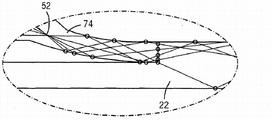
在图6~11B所示的另一系列的实施例中,各种光学组件可被组合使用,以进一步并明显提高聚集效率和收集效率两者。在最优选的实施例中,图6示出弯曲聚集元件50,该弯曲聚集元件50将光52引到弯曲反射器54上,该弯曲反射器54将光52转送到波导22中。在另一最优选的实施例中,图7示出另一弯曲聚集元件56,该弯曲聚集元件56将光52引出具有通过TIR将光52重定向到波导22中的两个平面59和60的反射器58。图8A示出部分闭合光学元件64,该部分闭合光学元件64在界面66处将光52重定向、将光52反射离开弯曲反射器68,使得光52聚集于光学元件64的底部反射表面72之间的界面70上。从图8B的放大图最好地看出,波导22与反射表面72具有大致互补的角度匹配。In another series of embodiments shown in FIGS. 6-11B, various optical components may be used in combination to further and significantly increase both the concentration efficiency and the collection efficiency. In the most preferred embodiment, FIG. 6 shows a curved focusing element 50 that directs light 52 onto a
在图9A中,在另一最优选的实施例中,示出与图8A类似的系统,但是,光学元件65被闭合并与收集光52并将其传输到波导22的延伸波导74(光导管的形式)相耦合(从图9B最能看出)。In FIG. 9A, in another most preferred embodiment, a system similar to that of FIG. 8A is shown, however,
在图10A中,光学元件76被闭合,其中通过TIR从具有如图10B最好地示出的特定角度截面的反射表面77反射输入光52,这使得能够由反射离开表面80、81和82实现通过TIR收集光以及与波导22耦合。In FIG. 10A , optical element 76 is closed wherein
在图11A中,光学元件82与另一反射器84协作,以将光52从两个不同的光源82和84引入波导22中,由此,进一步确保收集入射到光学元件82的表面86上的所有光。在本实施例中,光学元件82和84承担聚集元件和反射元件两者的作用。In FIG. 11A ,
在图25中,弯曲聚集元件12将光14引到将光14转送到波导22中的(重定向部件18)上。聚集元件12和重定向元件18被示为同一物理部分上的两个不同的部件,而波导22被示为与第一物理部分耦合的第二物理部分。在图26中,弯曲聚集元件12将光14引到依次起作用的将光14转送到波导22中的两个反射器(重定向部件18)上。聚集元件12、重定向部件18和波导22均被示出为耦合在一起的单独的物理部分。与图26类似,图27将光14引入到波导22中。但是,重定向部件18和波导22被组合成一个结构。In FIG. 25 , curved concentrating
在图28中,折射聚集元件12将光引到重定向元件18上,该重定向元件18将光14反射到波导22中。重定向元件18优选作为渐进式台阶部件集成到波导结构中。在图29中,聚集元件12和重定向元件18与图28中所示的那些类似,但是,波导22的顶面形成角度,使得波导22沿其长度具有基本上均匀的截面厚度。In FIG. 28 , refractive concentrating
除了重定向元件18和波导22旋转使得波导基本上与聚集元件12的面平行以外,图30与图29类似。除了附加的一组重定向元件87以外,图31与图30类似,该组重定向元件87折射来自聚集元件的光从而使得光在重定向元件18上的入射角度比图30中的光的可比较的入射角度大。这例如更有利于重定向元件18的作为重定向机制的全内反射。除了波导22的顶面具有定制形状(tailored shape)88以外,图32与图31类似。定制形状88可用于例如将通过波导传播的光传送到在波导22的端部处的限定斑点或位置L。FIG. 30 is similar to FIG. 29 except that the redirecting
在图33中,重定向元件18集成到与承载聚集元件12和波导22的部分分开的单个部分中。重定向元件18可以为在本申请中前文描述的任意类型,并且被示出为与图6中的元件类似的弯曲反射元件。波导22包含被定位为接收来自重定向元件18的光的渐进式台阶部件89。除了波导22的基面90形成角度以使得波导沿其长度具有基本上均匀的截面厚度以外,图34与图33类似。图35和图36示出波导22的基面分别具有被示出为平坦刻面88和弯曲元件88的定制形状88。如图32中那样,定制形状88可用于例如将通过波导22传播的光传送到在波导22的端部处的限定斑点L。In FIG. 33 the redirecting
除了聚集元件12是菲涅耳透镜以外,图37与图30类似。例如可通过注射成型、热压印或微复制聚合物材料或适于这些处理的其它材料来制造菲涅耳透镜。Figure 37 is similar to Figure 30 except that the concentrating
与图33~36类似,图38示出在顶面上具有进入元件91的波导22。除了进入元件91被集成为单独的部分,该部分然后通过光学耦合层92在光学上附接于块体波导元件22的平坦顶面之外,图39示出类似的波导22。光进入元件因此被布置为在物理上与波导的主体不连续。这允许使用例如基于薄膜基板的制造处理以制作进入元件部件。图40示出在全光学设计的例子中操作的图39所示的波导22。聚集元件12将光14聚集到重定向元件18上,该重定向元件18将光14重定向以便经由进入元件91插入波导22中。Similar to Figures 33-36, Figure 38 shows the
除了包含聚集元件12的部分通过使用低指数粘接剂93与波导22光学耦合以外,图41与图30类似。该构造消除了聚集元件12与波导22之间的空气间隙,并由此减少了在光从聚集元件12行进到波导22时由菲涅耳反射效应导致的光学损失。低指数粘接剂93需要具有适当的折射率,为了使得能够通过利用全内反射使光在波导22内传播,该折射率低于波导22的折射率。低指数粘接剂93可例如为诸如DowCorning Sylgard184的硅酮弹性体。除了聚集元件12是菲涅耳透镜而不是不对称块体透镜(bulk lens)以外,图42与图41类似。FIG. 41 is similar to FIG. 30 except that the portion containing the focusing
在图43中,聚集元件12将光14引向第一重定向元件87,该第一重定向元件87折射光14,将光14引到第二重定向元件18上,该第二重定向元件18将光重定向到波导22中以进行传播。在图43中,第一重定向元件87是平坦刻面。除了第一重定向元件87在聚集元件12之前与光14交互以外,图44与图43类似。在图45中,波导22跨着其长度双向地或者沿多个方向传播光14。聚集元件12将光聚集到重定向元件18和94上,这两个重定向元件18和94沿相反的方向使光重定向到波导22中。该构造允许在波导22的两端聚集和收集光。In FIG. 43, focusing
在图46中,聚集元件12将光14聚集到重定向元件18上。重定向元件18具有两个部分:将光折射到块体光学器件中的平坦刻面95和将光反射到波导22中的另一平坦刻面96。重定向刻面95和96以及波导22被集成为单个部分。如前面在第0059段(第6页第1段)中描述的那样,波导的端部具有朝向接收器23将光向下重定向的刻面99。在本实施例中,波导22具有波导97作为其关于轴98的镜像。在波导22的端部处的二次光学器件的布置和波导22的对称布局的可与在本申请中示出的所有实施例一起实现,并且已在第0049段中被解释。In FIG. 46 , concentrating
在图1~46中描述的重定向元件18与相应的聚集元件12相关联,并且通过利用反射、全内反射和折射的光学机制中的至少一种将光传送到波导22中。重定向元件可以但不必须与聚集元件光学耦合并且物理分离。The redirecting
在以上在本申请中描述的各种实施例中,聚集元件12通过层与相关联的重定向元件18的至少一部分分开。光14在该层内不经受方向的任何重新定位变化。层本身在相关联的重定向元件18中的每一个的至少一部分之间连续。该分离层使得聚集元件12和重定向元件18能够被设置在物理分离部件的垂直叠层中。这使得能够直接组装单独的部分以形成整个太阳聚集器。In the various embodiments described above in this application, the focusing
为了使成本最小化并简化设计,一个实际的挑战是通过强健的材料以尽可能少的部分实现所有上述功能。一般地,这涉及将多种功能结合到仅仅几个部分中。例如,通过将光学部件构图至盖片玻璃中,可使得玻璃能够实现保护模块并用作聚集元件12两者,同时保留其用作各种光学涂层的基板的能力。通过向软化玻璃应用具有经加工的同心部件的圆柱金属辊,大型玻璃制造设施可例行地在片材的一侧形成适度透镜特征。给定用以压印光学部件的合适辊设计,可在盖片玻璃上构图成线状透镜以形成一次光学(聚集)元件12。聚集元件12可在向外方向和向内方向两者上被取向,同时保留功能。向外部件具有微粒蓄积(这也称为污染)的危险,这对光传输有害。除了经操作的盖片玻璃方法以外,还可以通过使用诸如也提供聚光功能的硅酮沉积的处理向平坦盖片玻璃添加部件。To minimize cost and simplify design, a practical challenge is to achieve all of the above functions with as few parts as possible through robust materials. Typically, this involves combining multiple functions into just a few parts. For example, by patterning optical components into the cover glass, the glass can be enabled to both protect the module and serve as the concentrating
此外,可构造互补的二次光学部分,其用作用于来自盖片玻璃层的经聚集的光14的重定向元件18,并用作向接收器23传送重定向光14的波导22(图46)。应注意,在本实施例中,一次光学器件用作保护盖片玻璃和聚集层两者,而重定向功能和波导功能可被组合在该二次光学器件中。类似地,对于点聚焦设计,可以通过使用热压印或模具类型处理向玻璃施加轴对称透镜图案。Furthermore, a complementary secondary optic can be constructed that acts as a redirecting
将光学功能结合到盖片玻璃中并将重定向和波导到聚焦区的功能组合到一个部分中使得能够仅通过两个部分来管理或实现整个光路。此两部分类型的ATIR光学器件的一个关键方面在于:波导或二次光学器件的垂直位置和水平位置两者必须相对于一次光学层(盖片玻璃)被良好地保持。在其它的方面,保持分离层的几何形状对于确保强健的功能性是关键的。一种实现这一点的方式是将又一功能结合到一次或二次/波导光学部分中。例如,如图47所示,通过将定位元件或肋部部件100结合到二次光学器件中,能够在机械上互锁一次和二次光学部分,从而在垂直和水平维度两者中约束它们以确保稳定的分离。定位元件100因此在水平、垂直和旋转面内保持多个光学元件与波导之间的几何关系。Incorporating optical functions into the cover glass and combining the functions of redirection and waveguiding into the focal region into one part enables the entire optical path to be managed or realized with only two parts. A key aspect of this two-part type of ATIR optic is that both the vertical and horizontal position of the waveguide or secondary optic must be well maintained relative to the primary optical layer (cover glass). Among other things, maintaining the geometry of the separation layer is critical to ensure robust functionality. One way to achieve this is to incorporate yet another function into the primary or secondary/waveguide optics. For example, as shown in FIG. 47, by incorporating a positioning element or
用于生产的另一种选择是创建单独的支撑定位元件或肋部部件(rib feature)100。该选项具有必须制作另一单独的部分的缺点。但是,肋部部件非常简单,以致于用于将该部分成型的加工成本可以为低,并且,组件变得更模块化-从而允许实现在组装肋部和二次光学部分的方面的设计灵活性。图48示出说明互补的光学二次和支撑肋部部件100的示图。这些部分可以模块的方式被组装以提供设计灵活性。因此,定位元件100可以是波导的一体化部分或与波导分开的元件。Another option for production is to create a separate support positioning element or
可能的是,可行的接收器可由多个离散的光伏太阳电池构成。当将太阳能电池串联在一起时,可取的是在电池之间留下间隙,以管理焊接部周围的应力集中并使电池破坏减少到最少。这些间隙的影响是减少了可由其收集光能的面积。这些间隙是用于定位诸如定位元件或肋部100的非光学活性支撑部件的可用位置。并且,光学器件可通过光学重定向元件或缺口部件101被调整,以将否则会落于间隙上的光的大部分引向活动接收器(图49)。缺口部件101与重定向元件类似,但在波导22的不同的面中取向,以便在内部反射光以使其离开间隙并到达活动接收器上。缺口或横向光学元件101与波导22耦合,并且将横向的光重定向到波导22内的光传播方向。前面已经描述了与波导耦合并将来自波导的光重定向到光接收器的二次光学元件27。当利用上述的横向光学元件101时,二次光学元件27将来自波导和来自横向光学元件的光重定向到光接收器。Possibly, a feasible receiver could consist of multiple discrete photovoltaic solar cells. When connecting solar cells together in series, it is desirable to leave gaps between the cells to manage stress concentrations around the welds and minimize cell damage. The effect of these gaps is to reduce the area from which light energy can be collected. These gaps are available locations for positioning non-optically active support components such as positioning elements or
已出于解释和描述的目的给出了本发明的实施例的以上的描述。它不是详尽的,也不是要将本发明局限于公开的确切形式,并且,鉴于以上的教导可进行修改或变型,或者可从本发明的实际获取这些修改或变更。实施例被选择和描述以便解释本发明的原理及其实际应用,以使得本领域技术人员能够在各种实施例中以及通过适于设想的特定用途的各种修改来利用本发明。The foregoing description of the embodiments of the present invention have been presented for purposes of illustration and description. It is not intended to be exhaustive or to limit the invention to the precise form disclosed, and modifications or variations are possible in light of the above teaching or may be learned from practice of the invention. The embodiment was chosen and described in order to explain the principles of the invention and its practical application, to enable others skilled in the art to utilize the invention in various embodiments and with various modifications as are suited to the particular use contemplated.
Claims (18)
Applications Claiming Priority (3)
| Application Number | Priority Date | Filing Date | Title |
|---|---|---|---|
| US12/939,348 | 2010-11-04 | ||
| US12/939,348 US8412010B2 (en) | 2007-09-10 | 2010-11-04 | Compact optics for concentration and illumination systems |
| PCT/US2011/058144 WO2012061204A2 (en) | 2010-11-04 | 2011-10-27 | Compact optics for concentration and illumination systems |
Publications (1)
| Publication Number | Publication Date |
|---|---|
| CN103201657A true CN103201657A (en) | 2013-07-10 |
Family
ID=46025031
Family Applications (1)
| Application Number | Title | Priority Date | Filing Date |
|---|---|---|---|
| CN2011800531452A Pending CN103201657A (en) | 2010-11-04 | 2011-10-27 | Compact optics for concentration and illumination systems |
Country Status (8)
| Country | Link |
|---|---|
| US (1) | US8412010B2 (en) |
| EP (1) | EP2635929A4 (en) |
| JP (1) | JP5944400B2 (en) |
| KR (1) | KR20130140690A (en) |
| CN (1) | CN103201657A (en) |
| AU (1) | AU2011323696B2 (en) |
| CA (1) | CA2816065C (en) |
| WO (1) | WO2012061204A2 (en) |
Families Citing this family (36)
| Publication number | Priority date | Publication date | Assignee | Title |
|---|---|---|---|---|
| EP2645426A1 (en) | 2007-05-01 | 2013-10-02 | Morgan Solar Inc. | Light-guide solar panel and method of fabrication thereof |
| US8705914B2 (en) * | 2007-09-10 | 2014-04-22 | Banyan Energy, Inc. | Redirecting optics for concentration and illumination systems |
| US8817377B2 (en) * | 2009-05-14 | 2014-08-26 | Sunboost Ltd | Light collection system and method |
| TWI400812B (en) * | 2010-06-30 | 2013-07-01 | 晶元光電股份有限公司 | Solar battery module and electromagnetic wave collecting device thereof |
| US8885995B2 (en) | 2011-02-07 | 2014-11-11 | Morgan Solar Inc. | Light-guide solar energy concentrator |
| TWI538239B (en) * | 2011-02-14 | 2016-06-11 | Light collection device and its light collection method | |
| US8328403B1 (en) | 2012-03-21 | 2012-12-11 | Morgan Solar Inc. | Light guide illumination devices |
| US9261659B2 (en) | 2012-09-22 | 2016-02-16 | Solar Sure Pty Ltd. | Apparatus for concentrating solar energy |
| US9366396B2 (en) | 2013-01-30 | 2016-06-14 | Cree, Inc. | Optical waveguide and lamp including same |
| US9442243B2 (en) | 2013-01-30 | 2016-09-13 | Cree, Inc. | Waveguide bodies including redirection features and methods of producing same |
| US10436969B2 (en) | 2013-01-30 | 2019-10-08 | Ideal Industries Lighting Llc | Optical waveguide and luminaire incorporating same |
| US9291320B2 (en) | 2013-01-30 | 2016-03-22 | Cree, Inc. | Consolidated troffer |
| US9869432B2 (en) | 2013-01-30 | 2018-01-16 | Cree, Inc. | Luminaires using waveguide bodies and optical elements |
| US9690029B2 (en) | 2013-01-30 | 2017-06-27 | Cree, Inc. | Optical waveguides and luminaires incorporating same |
| US9625638B2 (en) | 2013-03-15 | 2017-04-18 | Cree, Inc. | Optical waveguide body |
| US9411086B2 (en) | 2013-01-30 | 2016-08-09 | Cree, Inc. | Optical waveguide assembly and light engine including same |
| WO2014141204A1 (en) * | 2013-03-15 | 2014-09-18 | Morgan Solar Inc. | Optics for illumination devices and solar concentrators |
| US9960303B2 (en) | 2013-03-15 | 2018-05-01 | Morgan Solar Inc. | Sunlight concentrating and harvesting device |
| US10502899B2 (en) * | 2013-03-15 | 2019-12-10 | Ideal Industries Lighting Llc | Outdoor and/or enclosed structure LED luminaire |
| US10436970B2 (en) * | 2013-03-15 | 2019-10-08 | Ideal Industries Lighting Llc | Shaped optical waveguide bodies |
| US9714756B2 (en) | 2013-03-15 | 2017-07-25 | Morgan Solar Inc. | Illumination device |
| US9798072B2 (en) | 2013-03-15 | 2017-10-24 | Cree, Inc. | Optical element and method of forming an optical element |
| US10379278B2 (en) * | 2013-03-15 | 2019-08-13 | Ideal Industries Lighting Llc | Outdoor and/or enclosed structure LED luminaire outdoor and/or enclosed structure LED luminaire having outward illumination |
| US9366799B2 (en) | 2013-03-15 | 2016-06-14 | Cree, Inc. | Optical waveguide bodies and luminaires utilizing same |
| US9595627B2 (en) | 2013-03-15 | 2017-03-14 | John Paul Morgan | Photovoltaic panel |
| WO2014138857A1 (en) | 2013-03-15 | 2014-09-18 | John Paul Morgan | Light panel, optical assembly with improved interface and light panel with improved manufacturing tolerances |
| US10400984B2 (en) | 2013-03-15 | 2019-09-03 | Cree, Inc. | LED light fixture and unitary optic member therefor |
| US10209429B2 (en) | 2013-03-15 | 2019-02-19 | Cree, Inc. | Luminaire with selectable luminous intensity pattern |
| US9920901B2 (en) | 2013-03-15 | 2018-03-20 | Cree, Inc. | LED lensing arrangement |
| JP2015099336A (en) * | 2013-11-20 | 2015-05-28 | 株式会社東芝 | Optical element and optical device |
| DE102015105630B4 (en) | 2015-02-03 | 2019-02-14 | Helmholtz-Zentrum Berlin Für Materialien Und Energie Gmbh | Optoelectronic component array with optical waveguide structure |
| EP3054487A1 (en) | 2015-02-03 | 2016-08-10 | Helmholtz-Zentrum Berlin für Materialien und Energie GmbH | Optoelectronic construction element array with light guide structure |
| US11719882B2 (en) | 2016-05-06 | 2023-08-08 | Ideal Industries Lighting Llc | Waveguide-based light sources with dynamic beam shaping |
| US10416377B2 (en) | 2016-05-06 | 2019-09-17 | Cree, Inc. | Luminaire with controllable light emission |
| US10784391B2 (en) * | 2016-12-08 | 2020-09-22 | University Of Rochester | Multiple layer optics for light collecting and emitting apparatus |
| WO2023174522A1 (en) | 2022-03-15 | 2023-09-21 | Freshape Sa | Light collecting assembly |
Citations (3)
| Publication number | Priority date | Publication date | Assignee | Title |
|---|---|---|---|---|
| US20070165295A1 (en) * | 2006-01-18 | 2007-07-19 | Seoul National University Industry Foundation | Terahertz or infrared filter using shape resonance |
| CN101809377A (en) * | 2007-09-10 | 2010-08-18 | 榕树能量公司 | Compact optics for concentration, aggregation and illumination of light energy |
| CN101861655A (en) * | 2007-06-18 | 2010-10-13 | 益科博能源设备(三亚)有限公司 | Method and device for transmitting light generated in scattering medium by means of waveguide |
Family Cites Families (149)
| Publication number | Priority date | Publication date | Assignee | Title |
|---|---|---|---|---|
| US705778A (en) | 1901-11-07 | 1902-07-29 | William Leggett Mccabe | Portable conveyer. |
| US3780722A (en) | 1972-04-26 | 1973-12-25 | Us Navy | Fiber optical solar collector |
| US4029519A (en) | 1976-03-19 | 1977-06-14 | The United States Of America As Represented By The United States Energy Research And Development Administration | Solar collector having a solid transmission medium |
| US4074704A (en) * | 1976-05-28 | 1978-02-21 | Gellert Donald P | Process of and apparatus for solar heating and the like |
| US4357486A (en) | 1978-03-16 | 1982-11-02 | Atlantic Richfield Company | Luminescent solar collector |
| US4411490A (en) | 1980-08-18 | 1983-10-25 | Maurice Daniel | Apparatus for collecting, distributing and utilizing solar radiation |
| US4379944A (en) | 1981-02-05 | 1983-04-12 | Varian Associates, Inc. | Grooved solar cell for deployment at set angle |
| US4863224A (en) | 1981-10-06 | 1989-09-05 | Afian Viktor V | Solar concentrator and manufacturing method therefor |
| US4505264A (en) | 1983-12-27 | 1985-03-19 | Universite Laval | Electromagnetic wave concentrator |
| JPS61114214A (en) * | 1984-11-09 | 1986-05-31 | Shimizu Constr Co Ltd | Light collecting device |
| JPS62195601A (en) * | 1985-09-20 | 1987-08-28 | Nissho Giken Kk | Optical direction converter |
| US5353075A (en) | 1988-08-17 | 1994-10-04 | In Focus Systems, Inc. | Convertible flat panel display system |
| JPH0432102A (en) * | 1990-05-25 | 1992-02-04 | Sanyo Electric Co Ltd | Natural lighting device |
| US5828427A (en) | 1990-06-11 | 1998-10-27 | Reveo, Inc. | Computer-based image display systems having direct and projection modes of viewing |
| US5050946A (en) | 1990-09-27 | 1991-09-24 | Compaq Computer Corporation | Faceted light pipe |
| US5150960A (en) | 1991-12-06 | 1992-09-29 | General Motors Corporation | Rear license plate illumination |
| US5146354A (en) | 1991-05-07 | 1992-09-08 | Compaq Computer Corporation | LCD system with a backlight having a light source at a light pipe's edge and with the LCD enframed |
| JPH05142535A (en) | 1991-08-29 | 1993-06-11 | Meitaku Syst:Kk | Incident light supply device for edge light panel |
| WO1993006509A1 (en) | 1991-09-27 | 1993-04-01 | Yasuhiro Koike | Light-scattering light guide and its manufacture, and applied optics apparatus thereof |
| JPH05127161A (en) | 1991-11-07 | 1993-05-25 | Rohm Co Ltd | Liquid crystal display device and its backlight |
| KR970008351B1 (en) | 1991-12-03 | 1997-05-23 | 샤프 가부시끼가이샤 | Liquid crystal display |
| US5438484A (en) | 1991-12-06 | 1995-08-01 | Canon Kabushiki Kaisha | Surface lighting device and a display having such a lighting device |
| JP2692025B2 (en) | 1992-01-24 | 1997-12-17 | スタンレー電気株式会社 | Planar light emitter device |
| JP3025109B2 (en) | 1992-03-11 | 2000-03-27 | シャープ株式会社 | Light source and light source device |
| US6002829A (en) | 1992-03-23 | 1999-12-14 | Minnesota Mining And Manufacturing Company | Luminaire device |
| US5303322A (en) | 1992-03-23 | 1994-04-12 | Nioptics Corporation | Tapered multilayer luminaire devices |
| US5528720A (en) | 1992-03-23 | 1996-06-18 | Minnesota Mining And Manufacturing Co. | Tapered multilayer luminaire devices |
| US5237641A (en) | 1992-03-23 | 1993-08-17 | Nioptics Corporation | Tapered multilayer luminaire devices |
| US5806955A (en) | 1992-04-16 | 1998-09-15 | Tir Technologies, Inc. | TIR lens for waveguide injection |
| JP2980776B2 (en) | 1992-06-04 | 1999-11-22 | 東ソー株式会社 | Backlight |
| JP3136200B2 (en) | 1992-07-22 | 2001-02-19 | 株式会社日立製作所 | Liquid crystal display |
| DE4227468C2 (en) | 1992-08-20 | 2002-01-17 | Teves Gmbh Alfred | Electrical switch unit, in particular for controlling air conditioning systems in motor vehicles |
| US5323477A (en) | 1992-08-24 | 1994-06-21 | Motorola, Inc. | Contact array imager with integral waveguide and electronics |
| JPH0695112A (en) | 1992-09-16 | 1994-04-08 | Hitachi Ltd | Prism plate and information display device formed by using this plate |
| US5339179A (en) | 1992-10-01 | 1994-08-16 | International Business Machines Corp. | Edge-lit transflective non-emissive display with angled interface means on both sides of light conducting panel |
| US5390276A (en) | 1992-10-08 | 1995-02-14 | Briteview Technologies | Backlighting assembly utilizing microprisms and especially suitable for use with a liquid crystal display |
| US5499165A (en) | 1992-10-08 | 1996-03-12 | Holmes, Jr.; Lawrence | Transparent edge-lit lighting pane for displays |
| US5359691A (en) | 1992-10-08 | 1994-10-25 | Briteview Technologies | Backlighting system with a multi-reflection light injection system and using microprisms |
| US5432876C1 (en) | 1992-10-19 | 2002-05-21 | Minnesota Mining & Mfg | Illumination devices and optical fibres for use therein |
| US5400224A (en) | 1993-01-08 | 1995-03-21 | Precision Lamp, Inc. | Lighting panel |
| KR0158247B1 (en) | 1993-01-19 | 1999-03-20 | 미따라이 하지메 | A light guide, an illuminating device having the light guide, and an image reading device and an information processing device having the illuminating device |
| JPH06314069A (en) | 1993-03-03 | 1994-11-08 | Fujitsu Ltd | Lighting equipment |
| JP3051591B2 (en) | 1993-03-05 | 2000-06-12 | 日本メジフィジックス株式会社 | Anti-adhesion agent for thallium-201 container |
| US6111622A (en) | 1993-03-12 | 2000-08-29 | Ois Optical Imaging Systems, Inc. | Day/night backlight for a liquid crystal display |
| AU6524694A (en) | 1993-03-29 | 1994-10-24 | Precision Lamp, Inc. | Flat thin uniform thickness large area light source |
| JP3781441B2 (en) | 1993-07-23 | 2006-05-31 | 康博 小池 | Light scattering light guide light source device and liquid crystal display device |
| US5485354A (en) | 1993-09-09 | 1996-01-16 | Precision Lamp, Inc. | Flat panel display lighting system |
| US5455882A (en) | 1993-09-29 | 1995-10-03 | Associated Universities, Inc. | Interactive optical panel |
| US5440197A (en) | 1993-10-05 | 1995-08-08 | Tir Technologies, Inc. | Backlighting apparatus for uniformly illuminating a display panel |
| EP0722576B1 (en) | 1993-10-05 | 2001-08-01 | Tir Technologies, Inc. | Light source for backlighting |
| US6313892B2 (en) | 1993-10-05 | 2001-11-06 | Teledyne Lighting And Display Products, Inc. | Light source utilizing reflective cavity having sloped side surfaces |
| US5428468A (en) | 1993-11-05 | 1995-06-27 | Alliedsignal Inc. | Illumination system employing an array of microprisms |
| US5396350A (en) | 1993-11-05 | 1995-03-07 | Alliedsignal Inc. | Backlighting apparatus employing an array of microprisms |
| US5521725A (en) | 1993-11-05 | 1996-05-28 | Alliedsignal Inc. | Illumination system employing an array of microprisms |
| US5555329A (en) | 1993-11-05 | 1996-09-10 | Alliesignal Inc. | Light directing optical structure |
| US6129439A (en) | 1993-11-05 | 2000-10-10 | Alliedsignal Inc. | Illumination system employing an array of multi-faceted microprisms |
| US5477239A (en) | 1993-11-12 | 1995-12-19 | Dell Usa, L.P. | Front lighting system for liquid crystal display |
| US5598281A (en) | 1993-11-19 | 1997-01-28 | Alliedsignal Inc. | Backlight assembly for improved illumination employing tapered optical elements |
| US5390085A (en) | 1993-11-19 | 1995-02-14 | Motorola, Inc. | Light diffuser for a liquid crystal display |
| US5479275A (en) | 1993-12-03 | 1995-12-26 | Ois Optical Imaging Systems, Inc. | Backlit liquid crystal display with integral collimating, refracting, and reflecting means which refracts and collimates light from a first light source and reflects light from a second light source |
| US5485291A (en) | 1994-02-22 | 1996-01-16 | Precision Lamp, Inc. | Uniformly thin, high efficiency large area lighting panel with two facet grooves that are spaced apart and have light source facing facets with smaller slopes than the facets facing away from the light source |
| US5982540A (en) | 1994-03-16 | 1999-11-09 | Enplas Corporation | Surface light source device with polarization function |
| CA2134902C (en) | 1994-04-07 | 2000-05-16 | Friedrich Bertignoll | Light diffusing apparatus |
| JP3538220B2 (en) | 1994-05-25 | 2004-06-14 | 株式会社エンプラス | Corner light supply type surface light source device |
| US5671994A (en) | 1994-06-08 | 1997-09-30 | Clio Technologies, Inc. | Flat and transparent front-lighting system using microprisms |
| US5692066A (en) | 1994-09-20 | 1997-11-25 | Neopath, Inc. | Method and apparatus for image plane modulation pattern recognition |
| US5506929A (en) | 1994-10-19 | 1996-04-09 | Clio Technologies, Inc. | Light expanding system for producing a linear or planar light beam from a point-like light source |
| AU4409496A (en) | 1994-11-29 | 1996-06-19 | Precision Lamp, Inc. | Edge light for panel display |
| US5579134A (en) | 1994-11-30 | 1996-11-26 | Honeywell Inc. | Prismatic refracting optical array for liquid flat panel crystal display backlight |
| US5659643A (en) | 1995-01-23 | 1997-08-19 | Minnesota Mining And Manufacturing Company | Notched fiber array illumination device |
| JP3251452B2 (en) | 1995-01-31 | 2002-01-28 | シャープ株式会社 | Backlight device for liquid crystal display device |
| US5608837A (en) | 1995-05-15 | 1997-03-04 | Clio Technologies, Inc. | Transmissive type display and method capable of utilizing ambient light |
| US5621833A (en) | 1995-06-12 | 1997-04-15 | Lau; Ronnie C. | Superposition of two-dimensional arrays |
| US5631994A (en) | 1995-08-23 | 1997-05-20 | Minnesota Mining And Manufacturing Company | Structured surface light extraction overlay and illumination system |
| US5877874A (en) | 1995-08-24 | 1999-03-02 | Terrasun L.L.C. | Device for concentrating optical radiation |
| US6104454A (en) | 1995-11-22 | 2000-08-15 | Hitachi, Ltd | Liquid crystal display |
| US5710793A (en) | 1995-12-21 | 1998-01-20 | National Semiconductor Corporation | Error signal quantization method and hardware for mixed blind and decision directed equalization |
| US5905826A (en) | 1996-01-24 | 1999-05-18 | Minnesota Mining And Manufacturing Co. | Conspicuity marking system including light guide and retroreflective structure |
| US6072551A (en) | 1996-02-14 | 2000-06-06 | Physical Optics Corporation | Backlight apparatus for illuminating a display with controlled light output characteristics |
| US5838403A (en) | 1996-02-14 | 1998-11-17 | Physical Optics Corporation | Liquid crystal display system with internally reflecting waveguide for backlighting and non-Lambertian diffusing |
| DE19610816C2 (en) | 1996-03-19 | 1999-02-04 | Ctx Opto Electronics Corp | Backlight system for a scoreboard |
| US5926601A (en) | 1996-05-02 | 1999-07-20 | Briteview Technologies, Inc. | Stacked backlighting system using microprisms |
| US5914760A (en) | 1996-06-21 | 1999-06-22 | Casio Computer Co., Ltd. | Surface light source device and liquid crystal display device using the same |
| US6005343A (en) | 1996-08-30 | 1999-12-21 | Rakhimov; Alexander Tursunovich | High intensity lamp |
| US5870156A (en) | 1996-09-05 | 1999-02-09 | Northern Telecom Limited | Shadow mask for backlit LCD |
| US5854872A (en) | 1996-10-08 | 1998-12-29 | Clio Technologies, Inc. | Divergent angle rotator system and method for collimating light beams |
| JPH10221528A (en) | 1996-12-05 | 1998-08-21 | Toyota Motor Corp | Solar cell equipment |
| US6473554B1 (en) | 1996-12-12 | 2002-10-29 | Teledyne Lighting And Display Products, Inc. | Lighting apparatus having low profile |
| DE69836042T2 (en) | 1997-03-04 | 2007-02-22 | Matsushita Electric Industrial Co., Ltd., Kadoma | Linear lighting device |
| US6007209A (en) | 1997-03-19 | 1999-12-28 | Teledyne Industries, Inc. | Light source for backlighting |
| US6123431A (en) | 1997-03-19 | 2000-09-26 | Sanyo Electric Co., Ltd | Backlight apparatus and light guide plate |
| EP0867747A3 (en) | 1997-03-25 | 1999-03-03 | Sony Corporation | Reflective display device |
| US6879354B1 (en) | 1997-03-28 | 2005-04-12 | Sharp Kabushiki Kaisha | Front-illuminating device and a reflection-type liquid crystal display using such a device |
| US6992733B1 (en) | 1997-04-11 | 2006-01-31 | Micron Technology, Inc. | Backlighting system for an LCD |
| PT1015811E (en) | 1997-09-19 | 2001-11-30 | Decoma Int Inc | OPTICAL DEVICE FOR LIGHT SEPARATION OF LARGE AND SMALL INTENSITY |
| US6021007A (en) | 1997-10-18 | 2000-02-01 | Murtha; R. Michael | Side-collecting lightguide |
| US6057505A (en) | 1997-11-21 | 2000-05-02 | Ortabasi; Ugur | Space concentrator for advanced solar cells |
| US6151089A (en) | 1998-01-20 | 2000-11-21 | Sony Corporation | Reflection type display with light waveguide with inclined and planar surface sections |
| US6497939B1 (en) | 1998-02-03 | 2002-12-24 | Nippon Zeon Co., Ltd. | Flat plate and light guide plate |
| JPH11259007A (en) | 1998-03-10 | 1999-09-24 | Sony Corp | Reflective display |
| US6134092A (en) | 1998-04-08 | 2000-10-17 | Teledyne Lighting And Display Products, Inc. | Illumination device for non-emissive displays |
| JP3119241B2 (en) | 1998-07-01 | 2000-12-18 | 日本電気株式会社 | Liquid crystal display |
| US6428198B1 (en) | 1998-07-07 | 2002-08-06 | Alliedsignal Inc. | Display system having a light source separate from a display device |
| US6234656B1 (en) | 1998-08-20 | 2001-05-22 | Physical Optics Corporation | Fiber optic luminaire |
| JP2000147262A (en) * | 1998-11-11 | 2000-05-26 | Nobuyuki Higuchi | Converging device and photovoltaic power generation system utilizing the device |
| GB9905642D0 (en) | 1999-03-11 | 1999-05-05 | Imperial College | Light concentrator for PV cells |
| US6623132B2 (en) | 1999-08-11 | 2003-09-23 | North American Lighting, Inc. | Light coupler hingedly attached to a light guide for automotive lighting |
| JP2001127331A (en) | 1999-10-29 | 2001-05-11 | Sanyo Electric Co Ltd | Solar cell module |
| US6440769B2 (en) | 1999-11-26 | 2002-08-27 | The Trustees Of Princeton University | Photovoltaic device with optical concentrator and method of making the same |
| US6347874B1 (en) | 2000-02-16 | 2002-02-19 | 3M Innovative Properties Company | Wedge light extractor with risers |
| JP2001289515A (en) * | 2000-04-07 | 2001-10-19 | Masahiro Nishikawa | Planar solar ray concentrating device |
| US6639349B1 (en) | 2000-06-16 | 2003-10-28 | Rockwell Collins, Inc. | Dual-mode LCD backlight |
| JP3932407B2 (en) | 2000-07-03 | 2007-06-20 | ミネベア株式会社 | Surface lighting device |
| JP2002289900A (en) | 2001-03-23 | 2002-10-04 | Canon Inc | Concentrating solar cell module and concentrating solar power generation system |
| US6738051B2 (en) | 2001-04-06 | 2004-05-18 | 3M Innovative Properties Company | Frontlit illuminated touch panel |
| US6592234B2 (en) | 2001-04-06 | 2003-07-15 | 3M Innovative Properties Company | Frontlit display |
| KR100765138B1 (en) | 2001-04-09 | 2007-10-15 | 삼성전자주식회사 | Backlight Assembly and Liquid Crystal Display Using Same |
| US6957904B2 (en) | 2001-07-30 | 2005-10-25 | 3M Innovative Properties Company | Illumination device utilizing displaced radiation patterns |
| US6576887B2 (en) | 2001-08-15 | 2003-06-10 | 3M Innovative Properties Company | Light guide for use with backlit display |
| KR100789138B1 (en) | 2001-09-05 | 2007-12-27 | 삼성전자주식회사 | Lighting device and reflection type liquid crystal display device using the same |
| US6966684B2 (en) | 2001-09-13 | 2005-11-22 | Gelcore, Llc | Optical wave guide |
| KR100403599B1 (en) * | 2001-11-06 | 2003-10-30 | 삼성전자주식회사 | Illumination system and a projection system imploying it |
| DE20200571U1 (en) | 2002-01-15 | 2002-04-11 | FER Fahrzeugelektrik GmbH, 99817 Eisenach | vehicle light |
| US6796700B2 (en) | 2002-02-02 | 2004-09-28 | Edward Robert Kraft | Flat panel luminaire with remote light source and hollow light pipe for back lit signage applications |
| US6986660B2 (en) | 2002-06-04 | 2006-01-17 | Zimmer Dental, Inc. | Retaining screw with rententive feature |
| JP2004047753A (en) * | 2002-07-12 | 2004-02-12 | Bridgestone Corp | Solar cell with condensing element |
| JP3923867B2 (en) | 2002-07-26 | 2007-06-06 | 株式会社アドバンスト・ディスプレイ | Planar light source device and liquid crystal display device using the same |
| US6842571B2 (en) | 2002-09-05 | 2005-01-11 | Motorola, Inc. | Optical interconnect system with layered lightpipe |
| US7063449B2 (en) | 2002-11-21 | 2006-06-20 | Element Labs, Inc. | Light emitting diode (LED) picture element |
| JP3767544B2 (en) | 2002-11-25 | 2006-04-19 | セイコーエプソン株式会社 | Optical device, illumination device, and projector |
| JP3776082B2 (en) | 2002-12-19 | 2006-05-17 | シャープ株式会社 | Solar cell module |
| JP2007027150A (en) * | 2003-06-23 | 2007-02-01 | Hitachi Chem Co Ltd | Concentrating photovoltaic system |
| US6966661B2 (en) | 2003-09-16 | 2005-11-22 | Robert L. Read | Half-round total internal reflection magnifying prism |
| JP4262113B2 (en) | 2004-02-13 | 2009-05-13 | シチズン電子株式会社 | Backlight |
| CN101076744B (en) | 2004-04-23 | 2010-05-12 | 光处方革新有限公司 | Optical manifold for light emitting diodes |
| CN101163932A (en) | 2004-12-17 | 2008-04-16 | 环球生物传感器有限公司 | electromagnetic radiation collector |
| US20060174867A1 (en) | 2004-12-28 | 2006-08-10 | Applied Optical Materials | Nonimaging solar collector/concentrator |
| WO2006085339A2 (en) | 2005-02-10 | 2006-08-17 | Instapower Ltd. | A lighting device |
| US7682761B2 (en) * | 2007-02-20 | 2010-03-23 | Sharp Laboratories Of America, Inc. | Method of fabricating a grayscale mask using a wafer bonding process |
| EP2645426A1 (en) * | 2007-05-01 | 2013-10-02 | Morgan Solar Inc. | Light-guide solar panel and method of fabrication thereof |
| US7672549B2 (en) | 2007-09-10 | 2010-03-02 | Banyan Energy, Inc. | Solar energy concentrator |
| WO2009063416A2 (en) * | 2007-11-13 | 2009-05-22 | Koninklijke Philips Electronics, N.V. | Thin and efficient collecting optics for solar system |
| US20090126792A1 (en) * | 2007-11-16 | 2009-05-21 | Qualcomm Incorporated | Thin film solar concentrator/collector |
| US7878190B2 (en) * | 2007-11-28 | 2011-02-01 | Walter T Charlton | Solar collection apparatus, solar collection arrays, and related methods |
| KR20110069071A (en) * | 2008-09-18 | 2011-06-22 | 퀄컴 엠이엠스 테크놀로지스, 인크. | Increased light collection angle range in solar collectors / concentrators |
| ES2364665B1 (en) | 2008-11-12 | 2012-05-23 | Abengoa Solar New Technologies, S.A. | LIGHTING AND CONCENTRATION SYSTEM. |
| US20100212717A1 (en) * | 2009-02-20 | 2010-08-26 | Whitlock John P | Solar collector with optical waveguide |
| US9256007B2 (en) * | 2009-04-21 | 2016-02-09 | Svv Technology Innovations, Inc. | Light collection and illumination systems employing planar waveguide |
| CN102483484A (en) * | 2009-06-24 | 2012-05-30 | 罗切斯特大学 | Dimpled light collection and concentration system, components thereof, and methods |
-
2010
- 2010-11-04 US US12/939,348 patent/US8412010B2/en not_active Expired - Fee Related
-
2011
- 2011-10-27 EP EP11838569.9A patent/EP2635929A4/en not_active Withdrawn
- 2011-10-27 CN CN2011800531452A patent/CN103201657A/en active Pending
- 2011-10-27 WO PCT/US2011/058144 patent/WO2012061204A2/en not_active Ceased
- 2011-10-27 JP JP2013537705A patent/JP5944400B2/en not_active Expired - Fee Related
- 2011-10-27 AU AU2011323696A patent/AU2011323696B2/en not_active Expired - Fee Related
- 2011-10-27 CA CA2816065A patent/CA2816065C/en not_active Expired - Fee Related
- 2011-10-27 KR KR1020137010534A patent/KR20130140690A/en not_active Ceased
Patent Citations (3)
| Publication number | Priority date | Publication date | Assignee | Title |
|---|---|---|---|---|
| US20070165295A1 (en) * | 2006-01-18 | 2007-07-19 | Seoul National University Industry Foundation | Terahertz or infrared filter using shape resonance |
| CN101861655A (en) * | 2007-06-18 | 2010-10-13 | 益科博能源设备(三亚)有限公司 | Method and device for transmitting light generated in scattering medium by means of waveguide |
| CN101809377A (en) * | 2007-09-10 | 2010-08-18 | 榕树能量公司 | Compact optics for concentration, aggregation and illumination of light energy |
Also Published As
| Publication number | Publication date |
|---|---|
| US8412010B2 (en) | 2013-04-02 |
| JP2013543150A (en) | 2013-11-28 |
| AU2011323696B2 (en) | 2016-09-29 |
| CA2816065C (en) | 2016-08-30 |
| AU2011323696A2 (en) | 2013-08-15 |
| CA2816065A1 (en) | 2012-05-10 |
| EP2635929A2 (en) | 2013-09-11 |
| KR20130140690A (en) | 2013-12-24 |
| WO2012061204A2 (en) | 2012-05-10 |
| US20110096426A1 (en) | 2011-04-28 |
| AU2011323696A1 (en) | 2013-05-23 |
| WO2012061204A3 (en) | 2012-07-19 |
| JP5944400B2 (en) | 2016-07-05 |
| EP2635929A4 (en) | 2014-11-12 |
Similar Documents
| Publication | Publication Date | Title |
|---|---|---|
| CN103201657A (en) | Compact optics for concentration and illumination systems | |
| AU2008299119B2 (en) | Compact optics for concentration, aggregation and illumination of light energy | |
| US7672549B2 (en) | Solar energy concentrator | |
| CN102272538B (en) | Light collection and concentration system | |
| JP5944398B2 (en) | Turning optics for heat collection and lighting systems | |
| US8885995B2 (en) | Light-guide solar energy concentrator | |
| JP2010539428A6 (en) | Compact optical element that focuses, collects and illuminates light energy | |
| US9246038B2 (en) | Light collecting and emitting apparatus, method, and applications | |
| CN102216695A (en) | System and method for solar energy capture and related method of manufacturing | |
| WO2011153633A1 (en) | Monolithic photovoltaic solar concentrator | |
| AU2012223120B2 (en) | Compact optics for concentration, aggregation and illumination of light energy |
Legal Events
| Date | Code | Title | Description |
|---|---|---|---|
| C06 | Publication | ||
| PB01 | Publication | ||
| C10 | Entry into substantive examination | ||
| SE01 | Entry into force of request for substantive examination | ||
| WD01 | Invention patent application deemed withdrawn after publication | ||
| WD01 | Invention patent application deemed withdrawn after publication |
Application publication date: 20130710 |