KR20110069071A - Increased light collection angle range in solar collectors / concentrators - Google Patents
Increased light collection angle range in solar collectors / concentrators Download PDFInfo
- Publication number
- KR20110069071A KR20110069071A KR1020117008404A KR20117008404A KR20110069071A KR 20110069071 A KR20110069071 A KR 20110069071A KR 1020117008404 A KR1020117008404 A KR 1020117008404A KR 20117008404 A KR20117008404 A KR 20117008404A KR 20110069071 A KR20110069071 A KR 20110069071A
- Authority
- KR
- South Korea
- Prior art keywords
- light
- light guide
- collecting device
- features
- light collecting
- Prior art date
- Legal status (The legal status is an assumption and is not a legal conclusion. Google has not performed a legal analysis and makes no representation as to the accuracy of the status listed.)
- Withdrawn
Links
Images


Classifications
-
- H—ELECTRICITY
- H10—SEMICONDUCTOR DEVICES; ELECTRIC SOLID-STATE DEVICES NOT OTHERWISE PROVIDED FOR
- H10F—INORGANIC SEMICONDUCTOR DEVICES SENSITIVE TO INFRARED RADIATION, LIGHT, ELECTROMAGNETIC RADIATION OF SHORTER WAVELENGTH OR CORPUSCULAR RADIATION
- H10F77/00—Constructional details of devices covered by this subclass
- H10F77/40—Optical elements or arrangements
- H10F77/42—Optical elements or arrangements directly associated or integrated with photovoltaic cells, e.g. light-reflecting means or light-concentrating means
- H10F77/488—Reflecting light-concentrating means, e.g. parabolic mirrors or concentrators using total internal reflection
-
- Y—GENERAL TAGGING OF NEW TECHNOLOGICAL DEVELOPMENTS; GENERAL TAGGING OF CROSS-SECTIONAL TECHNOLOGIES SPANNING OVER SEVERAL SECTIONS OF THE IPC; TECHNICAL SUBJECTS COVERED BY FORMER USPC CROSS-REFERENCE ART COLLECTIONS [XRACs] AND DIGESTS
- Y02—TECHNOLOGIES OR APPLICATIONS FOR MITIGATION OR ADAPTATION AGAINST CLIMATE CHANGE
- Y02E—REDUCTION OF GREENHOUSE GAS [GHG] EMISSIONS, RELATED TO ENERGY GENERATION, TRANSMISSION OR DISTRIBUTION
- Y02E10/00—Energy generation through renewable energy sources
- Y02E10/50—Photovoltaic [PV] energy
- Y02E10/52—PV systems with concentrators
Landscapes
- Photovoltaic Devices (AREA)
- Optical Elements Other Than Lenses (AREA)
- Diffracting Gratings Or Hologram Optical Elements (AREA)
- Light Guides In General And Applications Therefor (AREA)
- Planar Illumination Modules (AREA)
Abstract
본 명세서에 기재된 각종 실시형태에서, 장치는 광전지(203)에 광학적으로 결합된 도광층(201) 위에 배치된 각도 전환층(209)을 포함한다. 상기 도광층의 표면들 중 하나 상에 복수개의 표면 구성부(202)가 형성되어 있다. 상기 표면 구성부(202)는 서로에 대해서 기울어져 있는 파세트를 포함할 수 있다. 각도 전환층(209)은 입체 구성부 혹은 표면-릴리프 구성부인 회절 구성부를 포함한다. 제1각도에서 상기 각도 전환층(209) 상에 입사되는 광(210, 211)은 제2각도에서 상기 도광층(201)을 향하여 방향전환되고 나서 상기 도광층(201)의 표면 구성부에 의해 제2각도에서 방향변화되어 다수의 전내부반사에 의해 상기 도광층(201)을 통해서 도광된다. 도광된 광은 광전지(203) 쪽으로 향하게 된다.In various embodiments described herein, the device includes an angle turning layer 209 disposed over the light guide layer 201 optically coupled to the photovoltaic cell 203. A plurality of surface features 202 are formed on one of the surfaces of the light guide layer. The surface features 202 may include facets that are inclined relative to one another. The angle turning layer 209 includes diffractive features that are three-dimensional or surface-relief features. Light 210 and 211 incident on the angle turning layer 209 at a first angle are turned toward the light guide layer 201 at a second angle and then by the surface constitution of the light guide layer 201. It is oriented at a second angle and is guided through the light guide layer 201 by a plurality of total internal reflections. The guided light is directed towards photocell 203.
Description
관련 출원에 대한 교차 참조Cross Reference to Related Applications
본 출원은 미국 가출원 제61/098,179호(출원일: 2008년 9월 18일, 발명의 명칭: "INCREASING THE ANGULAR RANGE OF LIGHT COLLECTION IN SOLAR COLLECTORS/CONCENTRATORS")(변리사 문서 번호 제QMRC.010PR호)에 대해 35 U.S.C. § 119(e) 하에 우선권을 주장하며, 이 기초 출원은 참조로 그의 전문이 명백히 본원에 원용된다.This application is filed in U.S. Provisional Application No. 61 / 098,179 (filed September 18, 2008, titled "INCREASING THE ANGULAR RANGE OF LIGHT COLLECTION IN SOLAR COLLECTORS / CONCENTRATORS"). About 35 USC Priority is provided under § 119 (e), which is hereby expressly incorporated by reference in its entirety.
발명의 기술 분야Technical field of invention
본 발명은 광 수집장치(즉, 집광장치)(light collector) 및 집중장치, 특히 태양 방사선을 수집하여 집중시키기 위하여 미세-구조 박막을 이용하는 것에 관한 것이다.The present invention relates to the use of micro-structured thin films for collecting and concentrating light collectors (ie light collectors) and concentrators, in particular solar radiation.
태양 에너지는 열 및 전기 등과 같은 다른 형태의 에너지로 변환될 수 있는 재생가능한 에너지 공급원이다. 재생가능한 에너지의 신뢰성 있는 공급원으로서 태양 에너지를 이용하는 주된 결점은 광 에너지를 열이나 전기로 변환시키는 데 있어서의 낮은 효율, 그리고 하루 중의 시간 및 한 해 중의 달에 따라 태양 에너지에서의 편차이다.Solar energy is a renewable energy source that can be converted into other forms of energy such as heat and electricity. The main drawbacks of using solar energy as a reliable source of renewable energy are the low efficiency in converting light energy into heat or electricity, and the variation in solar energy with time of day and month of the year.
광기전력(PV: Photovoltaic) 전지는 태양 에너지를 전기 에너지로 변환시키는 데 이용될 수 있다. PV 전지를 이용하는 시스템은 10 내지 20% 사이의 변환 효율을 지닐 수 있다. PV 전지는 매우 얇게 만들어질 수 있어, 태양 에너지를 이용하는 다른 장치처럼 커다랗거나 부피가 크지 않다. PV 전지는 수 밀리미터 내지 수십 센티미터의 크기의 범위일 수 있다. 하나의 PV 전지로부터의 개별적인 전기 출력은 수 밀리와트 내지 수 와트의 범위일 수 있다. 수개의 PV 전지는 전기적으로 접속될 수 있고 충분한 양의 전기를 생성하도록 패키지화될 수 있다.Photovoltaic (PV) cells can be used to convert solar energy into electrical energy. Systems using PV cells can have a conversion efficiency between 10 and 20%. PV cells can be made very thin, not as large or bulky as other devices that use solar energy. PV cells can range in size from a few millimeters to several tens of centimeters. Individual electrical output from one PV cell can range from several milliwatts to several watts. Several PV cells can be electrically connected and packaged to produce a sufficient amount of electricity.
태양광 집중장치(solar concentrator)는 PV 전지에서 보다 높은 변환 효율을 얻기 위하여 태양 에너지를 수집하여 집중시키는 데 이용될 수 있다. 예를 들어, 포물면경은 광 에너지를 열과 전기로 변환시키는 장치에 광을 수집하여 집중시키는 데 이용될 수 있다. 다른 종류의 렌즈 및 거울도 변환 효율을 상당히 증가시키는 데 이용될 수 있지만, 이들은 하루 중의 시간, 한 해 중의 달 혹은 기후 조건 등에 따라서 입수되는 태양 에너지의 양의 편차를 해소하지 못한다. 또한, 렌즈/미러를 이용하는 시스템은 태양광을 효율적으로 수집하여 집중시키는 데 필요한 당해 렌즈 및 미러가 커야만 하기 때문에 부피가 커지고 무거워지는 경향이 있다.Solar concentrators can be used to collect and concentrate solar energy to achieve higher conversion efficiency in PV cells. For example, parabolic mirrors can be used to collect and concentrate light in devices that convert light energy into heat and electricity. Other types of lenses and mirrors can also be used to significantly increase conversion efficiency, but they do not address variations in the amount of solar energy available depending on time of day, month of the year or weather conditions. In addition, systems utilizing lenses / mirrors tend to be bulky and heavy because the lenses and mirrors needed to efficiently collect and focus sunlight are large.
PV 전지는 위성 및 우주 왕복선에 전력을 제공하고, 전기를 주거 및 상업적 속성에 제공하며, 자동차 배터리 및 기타 네비게이션 기구를 충전시키는 등의 광범위한 용도에 이용될 수 있다. 따라서, 많은 용도에 대해서, 이들 광 수집장치 및/또는 집중장치의 크기가 컴팩트한 것이 바람직하다.PV cells can be used in a wide variety of applications, such as providing power to satellites and space shuttles, providing electricity to residential and commercial properties, charging car batteries and other navigation devices, and the like. Thus, for many applications, it is desirable that these light collectors and / or concentrators be compact in size.
본 명세서에 기재된 각종 실시형태는 주변광을 수집(즉, 집광)/집중시키고 해당 수집된 광을 광전지로 향하게 하는(즉, 지향시키는) 도광체를 포함한다. 상기 도광체는 해당 도광체에 대해서 전방에 배치된 하나 이상의 홀로그래픽 층(holographic layer)을 포함할 수 있다. 해당 홀로그래픽 층은 입체 홀로그램(volume hologram) 혹은 표면 릴리프 특성부(즉, 표면 릴리프 구성부)(surface relief feature)들을 포함할 수 있다. 상기 홀로그래픽 층들은 제1각도에서 입사하는 광을 방향전환시켜 복수개의 프리즘 구성부(prismatic feature) 쪽으로 제2각도에서 입사광을 방향변화시킬 수 있다. 상기 프리즘 구성부는 상기 도광체에 대해서 후방에 배치되어 있을 수 있다. 상기 프리즘 구성부 상에 입사된 광은 다수의 전내부 반사(TIR: total internal reflection)에 의해 상기 도광체를 통해 광을 전파시키도록 더욱 방향변화될 수 있다. 상기 프리즘 구성부는 광을 반사시키는 파세트(facet)들을 포함할 수 있다. 몇몇 실시형태에 있어서, 상기 파세트들은 서로에 대해서 각도를 이룰 수 있다(즉, 기울어져 있을 수 있다). 광전지는 상기 도광체에 대해서 광학적으로 결합되어 있다. 몇몇 실시형태에 있어서, 상기 광전지는 상기 도광체에 인접하게 배치될 수 있다. 몇몇 다른 실시형태에 있어서, 상기 광전지는 상기 도광체의 하나의 모서리부에 배치될 수 있다. 또 다른 실시형태에 있어서, 상기 광전지는 상기 도광체의 아래쪽에 배치될 수 있다. 몇몇 실시형태에 있어서, 상기 도광체는 기판 상에 배치될 수 있다. 기판은 유리, 플라스틱, 전색성 유리(electrochromic glass), 스마트 글래스(smart glass) 등을 포함할 수 있다.Various embodiments described herein include a light guide that collects (ie, collects) / concentrates ambient light and directs (ie, directs) the collected light to a photovoltaic cell. The light guide may comprise one or more holographic layers disposed in front of the light guide. The holographic layer may comprise a volume hologram or surface relief features (ie, surface relief features). The holographic layers may redirect incident light at a first angle to redirect incident light at a second angle toward a plurality of prismatic features. The prismatic features may be disposed behind the light guide. Light incident on the prismatic features may be further redirected to propagate light through the light guide by a plurality of total internal reflections (TIR). The prismatic features may include facets that reflect light. In some embodiments, the facets may be angled (ie, tilted) with respect to each other. Photocells are optically coupled to the light guide. In some embodiments, the photovoltaic cell can be disposed adjacent to the light guide. In some other embodiments, the photovoltaic cell can be disposed at one corner of the light guide. In yet another embodiment, the photovoltaic cell may be disposed below the light guide. In some embodiments, the light guide may be disposed on a substrate. Substrates can include glass, plastic, electrochromic glass, smart glass, and the like.
본 명세서에 기재된 각종 실시형태는 광수집장치를 포함한다. 해당 광수집장치는 상부면과 하부면을 구비한 도광수단을 포함한다. 각종 실시형태에서, 상기 도광수단은 상부면 및 하부면에서 다수의 전내부 반사에 의해 내부에 광을 도광하도록 구성되어 있다. 각종 실시형태에서, 상기 광수집장치는 광을 회절시키는 복수개의 회절수단을 포함하되, 해당 회절수단은 상기 도광수단의 상부면에 대한 법선(normal)에 대해서 제1각도에서 광을 수광하도록 배치되어 있다. 상기 광수집장치는 광을 방향전환시키는 복수개의 광 방향전환수단을 추가로 포함할 수 있고, 해당 광 방향전환수단은 상기 복수개의 회절수단의 후방에 배치되어 있다. 각종 실시형태에서, 상기 복수개의 회절수단은 상기 복수개의 광 방향전환수단을 향하여 제2각도에서 상기 광을 방향변화시키도록 구성되어 있다. 각종 실시형태에서, 상기 복수개의 광 방향전환수단은 상기 광이 상기 도광수단의 상부면과 하부면으로부터의 전내부반사에 의해 상기 도광체 내에 도광되게끔 상기 회절수단에 의해 방향변화된 광을 방향전환시키도록 구성되어 있다. 몇몇 실시형태에서, 상기 도광수단은 도광체를 포함하거나, 상기 복수개의 회절수단은 복수개의 회절 구성부를 포함하거나, 또는 상기 복수개의 광 방향전환수단은 복수개의 프리즘 구성부를 포함한다.Various embodiments described herein include a light collecting device. The light collecting device includes light guiding means having an upper surface and a lower surface. In various embodiments, the light guiding means are configured to guide light therein by a plurality of total internal reflections at the top and bottom surfaces. In various embodiments, the light collecting device includes a plurality of diffraction means for diffracting light, the diffraction means being arranged to receive light at a first angle with respect to a normal to an upper surface of the light guide means. have. The light collecting device may further include a plurality of light turning means for redirecting light, the light turning means being disposed behind the plurality of diffraction means. In various embodiments, the plurality of diffraction means is configured to redirect the light at a second angle towards the plurality of light turning means. In various embodiments, the plurality of light turning means redirects the light redirected by the diffraction means such that the light is guided in the light guide by total internal reflection from the top and bottom surfaces of the light guide means. It is configured to. In some embodiments, the light guiding means comprises a light guide, the plurality of diffractive means comprises a plurality of diffractive features, or the plurality of light turning means comprises a plurality of prismatic features.
각종 실시형태에서, 광수집장치를 제조하는 방법이 개시되어 있다. 해당 방법은 상부면과 하부면을 구비한 도광체를 제공하는 단계를 포함한다. 각종 실시형태에서, 상기 도광체는 상기 상부면과 하부면에서의 다수의 전내부반사에 의해 내부에 광을 도광시키도록 구성되어 있다. 상기 방법은 상기 도광체에 대해서 복수개의 회절 구성부를 제공하는 단계를 포함한다. 각종 실시형태에서, 상기 복수개의 회절 구성부는 상기 도광체의 상부면에 대한 법선에 대해서 제1각도에서 광을 수광하도록 구성되어 있다. 상기 방법은 상기 도광체에 대해서 복수개의 프리즘 구성부를 제공하는 단계를 추가로 포함할 수 있다. 각종 실시형태에서, 상기 복수개의 프리즘 구성부는 상기 복수개의 회절 구성부의 후방에 배치되어 있다. 각종 실시형태에서, 복수개의 프리즘 구성부는 상기 도광체의 후방에 배치되어 있을 수 있다. 각종 실시형태에서, 상기 복수개의 프리즘 구성부는 주조(molding), 엠보싱(embossing) 혹은 에칭에 의해 제공될 수 있다. 각종 실시형태에서, 상기 복수개의 회절 구성부는 상기 도광체의 전방에 배치되어 있을 수 있다. 몇몇 실시형태에서, 상기 복수개의 회절 구성부는 상기 도광체의 전방에 배치된 층 내에 제공될 수 있다.In various embodiments, a method of manufacturing a light collecting device is disclosed. The method includes providing a light guide having a top surface and a bottom surface. In various embodiments, the light guide is configured to guide light therein by a plurality of total internal reflections at the top and bottom surfaces. The method includes providing a plurality of diffractive features for the light guide. In various embodiments, the plurality of diffractive features are configured to receive light at a first angle with respect to the normal to the top surface of the light guide. The method may further comprise providing a plurality of prismatic features for the light guide. In various embodiments, the plurality of prismatic features are disposed behind the plurality of diffractive features. In various embodiments, a plurality of prismatic features may be disposed behind the light guide. In various embodiments, the plurality of prismatic features can be provided by casting, embossing, or etching. In various embodiments, the plurality of diffractive features may be disposed in front of the light guide. In some embodiments, the plurality of diffractive features may be provided in a layer disposed in front of the light guide.
본 명세서에 개시된 예시적인 실시형태는, 단지 예시의 목적을 위해 제공되는 첨부된 개략적인 도면을 참조하여 설명된다.The exemplary embodiments disclosed herein are described with reference to the accompanying schematic drawings, which are provided for illustrative purposes only.
도 1a는 도광체에 대해서 거의 수직 입사(normal incidence)로 입사된 광을 수집하여 광전지로 도광시키도록 구성된 복수개의 프리즘 구성부를 포함하는 프리즘 도광체의 측면도;
도 1b는 복수개의 프리즘 구성부의 확대된 측면도;
도 1c는 도 1a에 표시된 실시형태의 사시도;
도 1d는 소정 각도에서 입사하는 광을 도광시키지 않는 복수개의 프리즘 구성부를 포함하는 도광체의 측면도;
도 2a는 도광체 및 홀로그래픽 층을 포함하는 일 실시형태의 측면도로서, 상기 홀로그래픽 층은 상기 도광체의 하나의 가장자리부를 따라 배치된 광기전력 전지에 광을 수집하여 도광시키도록 구성되어 있는 다수의 홀로그램을 추가로 포함함;
도 2b는 프리즘 도광체 및 홀로그래픽 층을 포함하는 일 실시형태의 측면도로서, 상기 홀로그래픽 층은 상기 도광체의 두 가장자리부를 따라 배치된 두 광기전력 전지에 광을 수집하여 도광시키도록 구성되어 있는 다수의 홀로그램을 추가로 포함함;
도 3은 프리즘 도광체 및 다수의 홀로그래픽 층을 포함하는 일 실시형태의 측면도;
도 4a는 프리즘 구성부가 어긋나게 적층되어 있는 다수의 프리즘 도광체층 및 다수의 홀로그래픽 층을 포함하는 일 실시형태의 측면도;
도 4b는 상이한 형상을 지니는 프리즘 구성부를 지닌 단일의 프리즘 도광체 및 다수의 홀로그래픽 층을 포함하는 일 실시형태의 측면도;
도 5a는 중앙에 배치된 광전지가 동심적으로 배열된 프리즘 구성부를 지니는 도광체 및 홀로그래픽층을 포함하는 일 실시형태를 도시한 도면;
도 5b는 곡선의 프리즘 구성부를 구비한 도광체, 홀로그래픽 층 및 하나의 모서리부에 배치된 광전지를 포함하는 일 실시형태를 도시한 도면;
도 6은 홀로그래픽 막의 후방에 배치된 미세구조 패턴의 어레이를 도시한 도면;
도 7은 홀로그래픽 층을 포함하는 도광체가 해당 도광체 아래쪽에 있는 광전지로 광을 향하게 하도록 베벨(bevel)형상으로 되어 있는 일 실시형태를 도시한 도면;
도 8은 주거용 주택의 창 및 지붕에 설치된 광전지에 광학적으로 결합된 집광판, 집광시트 혹은 집광막을 도시한 도면;
도 9는 광전지에 광학적으로 결합된 집광판, 집광시트 혹은 집광막이 자동차의 지붕에 설치된 일 실시형태를 도시한 도면;
도 10은 광전지에 광학적으로 결합된 집광판, 집광시트 혹은 집광막이 랩톱(laptop)의 본체에 부착된 실시형태를 나타낸 도면;
도 11은 광전지에 광학적으로 결합된 집광판, 집광시트 혹은 집광막이 의류 제품에 부착된 일례를 도시한 도면;
도 12는 광전지에 광학적으로 결합된 집광판, 집광시트 혹은 집광막이 신발에 설치된 일례를 도시한 도면;
도 13은 광전지에 광학적으로 결합된 집광판, 집광시트 혹은 집광막이 비행기의 날개와 창에 부착된 일 실시형태를 나타낸 도면;
도 14는 광전지에 광학적으로 결합된 집광판, 집광시트 혹은 집광막이 요트(혹은 범선)(sail boat)에 부착된 일 실시형태를 나타낸 도면;
도 15는 광전지에 광학적으로 결합된 집광판, 집광시트 혹은 집광막이 자전거에 부착된 일 실시형태를 나타낸 도면;
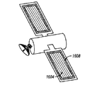
도 16은 광전지에 광학적으로 결합된 집광판, 집광시트 혹은 집광막이 위성에 부착된 일 실시형태를 나타낸 도면;
도 17은 둥글게 말을 수 있도록(rolled) 실질적으로 가요성인 집광시트가 광전지에 광학적으로 결합된 일 실시형태를 도시한 도면. 1A is a side view of a prismatic light guide comprising a plurality of prismatic features configured to collect and guide light into a photovoltaic cell that is incident at approximately normal incidence with respect to the light guide;
1B is an enlarged side view of a plurality of prismatic features;
1C is a perspective view of the embodiment shown in FIG. 1A;
1D is a side view of a light guide including a plurality of prismatic features that do not guide light incident at an angle;
FIG. 2A is a side view of an embodiment that includes a light guide and a holographic layer, wherein the holographic layer is configured to collect and guide light to a photovoltaic cell disposed along one edge of the light guide. Further comprising a hologram of;
2B is a side view of an embodiment that includes a prism light guide and a holographic layer, the holographic layer configured to collect and guide light to two photovoltaic cells disposed along two edges of the light guide. Further comprising a plurality of holograms;
3 is a side view of one embodiment including a prism light guide and a plurality of holographic layers;
FIG. 4A is a side view of an embodiment that includes a plurality of prism light guide layers and a plurality of holographic layers in which prismatic features are alternately stacked;
4B is a side view of an embodiment that includes a single prism light guide with multiple shaped prismatic features and multiple holographic layers;
FIG. 5A illustrates one embodiment including a light guide and a holographic layer having a prismatic arrangement with concentrically arranged photovoltaic cells;
FIG. 5B illustrates one embodiment including a light guide with curved prismatic features, a holographic layer, and a photovoltaic cell disposed at one corner;
6 shows an array of microstructured patterns disposed behind the holographic film;
FIG. 7 illustrates an embodiment in a bevel shape to direct a light guide comprising a holographic layer to direct light to a photovoltaic cell beneath the light guide.
8 illustrates a light collecting plate, sheet or film optically coupled to photovoltaic cells installed on the windows and roofs of residential homes;
FIG. 9 illustrates an embodiment in which a light collecting plate, sheet or film optically coupled to a photovoltaic cell is installed on the roof of an automobile;
10 shows an embodiment in which a light collecting plate, sheet or film optically coupled to a photovoltaic cell is attached to a body of a laptop;
11 shows an example in which a light collecting plate, sheet or film optically coupled to a photovoltaic cell is attached to a garment product;
12 illustrates an example in which a light collecting plate, sheet or film optically coupled to a photovoltaic cell is installed in a shoe;
13 illustrates an embodiment in which a light collecting plate, sheet or film optically coupled to a photovoltaic cell is attached to the wing and window of an airplane;
14 shows an embodiment in which a light collecting plate, sheet or film optically coupled to a photovoltaic cell is attached to a yacht (or sail boat);
15 shows an embodiment in which a light collecting plate, sheet or film optically coupled to a photovoltaic cell is attached to a bicycle;
FIG. 16 shows an embodiment in which a light collecting plate, sheet or film optically coupled to a photovoltaic cell is attached to a satellite;
FIG. 17 illustrates one embodiment in which a substantially flexible light collecting sheet is optically coupled to a photovoltaic cell so as to be rolled.
이하의 상세한 설명은 본 발명의 임의의 특정 실시형태들에 관한 것이지만, 본 발명은 다양한 방법들로 구현될 수 있다. 이하의 설명으로부터 명백한 바와 같이, 각 실시형태는 공급원으로부터의 광선을 수집, 포획 및 집중시키도록 구성된 장치이면 어떠한 장치에서도 구현될 수도 있다. 더욱 상세하게는, 거주 및 상업적 구조 및 속성에 전력을 제공하거나, 랩톱, PDA, 손목시계, 계산기, 휴대폰, 캠코더, 스틸 카메라, 비디오 카메라, MP3 플레이어 등과 같은 전자 기기에 전력을 제공하는, 다양한 용도에서 혹은 해당 다양한 용도와 관련해서 구현될 수도 있다. 또한, 본 명세서에 개시된 실시형태는 착용가능한 전력 발전 의류, 신발 및 액세서리에 이용될 수 있다. 본 명세서에 기재된 실시형태의 일부는 자동차 배터리, 네비게이션 기기, 물을 펌핑하는 기기를 충전하는 데 이용될 수 있다. 본 명세서에 기재된 실시형태는 항공 및 위성 용도에서의 이용도 발견할 수 있다. 기타 이용도 가능하다.Although the following detailed description relates to any particular embodiment of the present invention, the present invention may be implemented in various ways. As will be apparent from the description below, each embodiment may be implemented in any device as long as the device is configured to collect, capture, and focus light rays from a source. More specifically, various uses to power residential and commercial structures and properties, or to power electronic devices such as laptops, PDAs, watches, calculators, mobile phones, camcorders, still cameras, video cameras, MP3 players, and the like. It can also be implemented in or in conjunction with its various uses. In addition, the embodiments disclosed herein may be used in wearable power generating clothing, shoes and accessories. Some of the embodiments described herein can be used to charge car batteries, navigation devices, water pumping devices. Embodiments described herein may also find use in aviation and satellite applications. Others are also available.
본 명세서에 기재된 각종 실시형태에 있어서, 태양광 수집장치 및/또는 집중장치가 광전지에 결합되어 있다. 태양광 수집장치 및/또는 집중장치는 상부에 프리즘 방향전환 특성부(즉, 프리즘 방향전환 구성부)(prismatic turning feature)(이하 간단히 "프리즘 구성부"라 칭할 경우도 있음)를 지닌 도광체, 예를 들어, 판, 시트 혹은 막을 포함한다. 상기 도광체에 입사되는 주변광은 상기 프리즘 구성부에 의해 해당 도광체 내로 방향전환되어, 전내부 반사에 의해 해당 도광체를 통해 도광된다. 광전지는 상기 도광체의 하나 이상의 가장자리부를 따라 배치되고, 상기 도광체를 따라 전파된 광은 광전지에 결합된다. 주변광을 광전지에 수광, 집중 및 지향시키는 도광체를 이용하는 것은 증가된 효율과 낮아진 비용으로 광 에너지를 열 및 전기로 변환시키는 광-전기 장치를 실현할 수 있다. 상기 도광체는 판, 시트 혹은 막으로서 형성될 수 있다. 상기 도광체는 강성 혹은 반강성 재료(semi-rigid material)로 제작될 수 있다. 몇몇 실시형태에 있어서, 상기 도광체는 가요성 재료로 형성될 수 있다. 각종 실시형태에 있어서, 상기 도광체는 박막을 포함할 수 있다. 상기 도광체는 선형 방식으로 배열된 홈들을 포함할 수 있다. 몇몇 실시형태에 있어서, 상기 프리즘 구성부는 비선형 연장부를 지닐 수 있다. 예를 들어, 몇몇 실시형태에 있어서, 프리즘 구성부는 곡선을 따라 배열될 수 있다. 일 실시형태는 도광매체를 통해 분산된 원추형 반사 구성부를 지닌 박막 도광체로 구성될 수 있다.In various embodiments described herein, solar collectors and / or concentrators are coupled to photovoltaic cells. The solar collector and / or concentrator may be provided with a light guide having a prism turning feature (ie, sometimes simply referred to as a "prism feature") on top; For example, plates, sheets or membranes. Ambient light incident on the light guide is redirected into the light guide by the prismatic features and is guided through the light guide by total internal reflection. Photocells are disposed along one or more edges of the light guide, and light propagated along the light guide is coupled to the photocell. The use of light guides that receive, concentrate and direct ambient light to photovoltaic cells can realize opto-electric devices that convert light energy into heat and electricity at increased efficiency and lower cost. The light guide may be formed as a plate, sheet or film. The light guide may be made of a rigid or semi-rigid material. In some embodiments, the light guide may be formed of a flexible material. In various embodiments, the light guide may comprise a thin film. The light guide may comprise grooves arranged in a linear manner. In some embodiments, the prismatic features can have non-linear extensions. For example, in some embodiments, the prismatic features can be arranged along a curve. One embodiment may be comprised of a thin film light guide having conical reflective features dispersed through the light guide medium.
주변광을 광전지에 결합시키는 데 이용되는 프리즘 도광체의 일 실시형태가 도 1a에 도시되어 있다. 해당 광전지는 광기전력 전지 혹은 광검출기일 수 있다. 도 1a는 광전지(103)에 대해서 배치된 도광체(101)를 포함하는 실시형태(100)의 측면도를 예시하고 있다. 몇몇 실시형태에서, 상기 도광체(101)는 기판(도시 생략)을 추가로 포함할 수 있다. 복수개의 프리즘 구성부(102)가 상기 도광체(101) 내에 배치되어 있을 수 있다. 상기 도광체(101)는 상부면과 하부면을 포함할 수 있고, 해당 상부면과 하부면 사이에는 복수개의 가장자리부를 포함할 수 있다. 도 1a에 예시된 실시형태에서, 상기 프리즘 구성부는 상기 하부면 상에 배치되어 있다. 상기 도광체(101)에 입사되는 광은 상기 복수개의 프리즘 구성부(102)에 의해 상기 도광체(101) 내로 방향변화되어, 상기 상부면과 하부면에서의 다수의 전내부반사에 의해 해당 도광체(101) 내에 도광될 수 있다. 상기 도광체(101)는 광전지가 감응하는 하나 이상의 파장에서 방사선에 대해서 투명한 광학적으로 투과성인 재료를 포함할 수 있다. 예를 들어, 하나의 실시형태에서, 상기 도광체(101)는 가시광 및 근적외 영역 내의 파장에 대해서 광학적으로 투과성일 수 있다. 다른 실시형태에서, 상기 도광체(101)는 자외 혹은 적외 영역의 파장에 대해서 투명할 수 있다. 상기 도광체(101)는 상기 실시형태에 대해서 구조적 안정성을 제공하도록 유리, 아크릴, 폴리카보네이트, 폴리에스터 혹은 사이클로-올레핀 폴리머 등과 같은 강성 혹은 반강성(semi-rigid) 재료로 형성될 수 있다. 대안적으로, 도광체(101)는 가요성 폴리머 등과 같은 가요성 재료로 형성될 수 있다. 본 명세서에 구체적으로 언급된 것들 이외에 다른 재료도 이용될 수 있다.One embodiment of a prismatic light guide used to couple ambient light to a photovoltaic cell is shown in FIG. 1A. The photovoltaic cell may be a photovoltaic cell or a photodetector. 1A illustrates a side view of an
도광체(101)의 상부면은 주변광을 수광하도록 구성되어 있을 수 있다. 상기 도광체(101)는 가장자리부에 의해 완전히 둘러싸여 있다. 전형적으로는, 상기 도광체(101)의 길이와 폭은 해당 도광체(101)의 두께보다 실질적으로 크다. 상기 도광체(101)의 두께는 0.1 내지 10㎜에서 다양할 수 있다. 상기 도광체(101)의 면적은 0.01 내지 10,000㎠에서 다양할 수 있다. 그러나, 이들 범위 밖의 치수도 가능하다. 몇몇 실시형태에 있어서, 도광체(101)를 포함하는 재료의 굴절률은 전내부 반사(TIR)에 의해 도광체(101) 내에 주변광의 많은 부분을 도광하도록 주변보다 상당히 높을 수 있다.The upper surface of the
도광체(101) 내에 도광된 광은 해당 도광체 내의 흡수 및 다른 파세트로부터의 산란으로 인해 손실될 수도 있다. 도광된 광의 이러한 손실을 저감시키기 위하여, 몇몇 실시형태에서, 도광체(101)의 길이는 반사 횟수를 줄이도록 수십 인치로 제한될 수 있다. 그러나, 도광체(101)의 길이를 제한하는 것은 광이 수집되는 면적을 저감시킬 수 있다. 따라서, 몇몇 실시형태에서, 상기 도광체(101)의 길이는 수십 인치보다 크게 증가시킬 수도 있다. 몇몇 실시형태에서, 광학적 피복이 산란 손실을 저감시키기 위하여 상기 도광체(101)의 표면 상에 증착될 수 있다.Light guided in the
하나의 실시형태에서, 도 1a에 도시된 바와 같이, 도광체(101)는 해당 도광체(101)의 하부면 상에 배치된 프리즘 구성부(102)를 포함한다. 해당 프리즘 구성부는 도광체(101)의 하부면 상에 형성된 긴 홈부들(elongated grooves)을 포함할 수 있다. 이들 홈부는 광학적으로 투과성인 재료로 채워져 있을 수 있다. 상기 프리즘 구성부(102)는 주조, 엠보싱, 에칭 혹은 기타 대안적인 기법에 의해 도광체(101)의 하부면 상에 형성될 수 있다. 대안적으로, 프리즘 구성부(102)들은 도광체(101)의 하부면 상에 적층될 수 있는 막(혹은 필름) 상에 배치될 수 있다. 프리즘 필름을 포함하는 몇몇 실시형태에서, 광은 프리즘 필름 단독 내에 도광될 수 있다. 상기 프리즘 구성부(102)는 다양한 형상을 포함할 수 있다. 예를 들어, 상기 프리즘 구성부(102)는 선형 v자형 홈일 수 있다. 대안적으로, 상기 프리즘 구성부(102)는 곡선 홈 혹은 비선형 형상을 포함할 수 있다. 기타 다른 형태도 가능하다.In one embodiment, as shown in FIG. 1A, the
도 1b는 선형 v자형 홈(116)의 형태의 프리즘 구성부(102)의 확대도를 나타내고 있다. v자형 홈(116)은 도 1b에 도시된 바와 같이 서로에 대해서 각도 간격(α)으로 배열된 두 평탄한 파세트(F1), (F2)를 포함한다. 파세트들 간의 각도 간격(α)은 15° 내지 120°에서 변화될 수 있다. 몇몇 실시형태에 있어서, 파세트(F1), (F2)는 동일한 길이일 수 있다. 몇몇 다른 실시형태에 있어서, 파세트들 중 하나의 길이는 다른 것보다 클 수 있다. 두 연속적인 v자형 홈 간의 거리 'a'는 0.01 내지 0.5㎜에서 변화될 수 있다. 'b'로 표시된 v자형 홈의 폭은 0.001 내지 0.100㎜에서 변화될 수 있는 한편, 'd'로 표시된 v자형 홈의 깊이는 0.001 내지 0.5㎜에서 변화될 수 있다. 이들 범위 밖의 치수도 이용될 수 있다.1B shows an enlarged view of the
도 1c는 도 1a에 기재된 실시형태의 사시도를 도시하고 있다. 도 1c에 도시된 바와 같이, 도 1c에 기재된 실시형태는 도광체(101)의 하부면을 따라 배열된 선형 v자형 홈의 열들을 포함한다.FIG. 1C shows a perspective view of the embodiment described in FIG. 1A. As shown in FIG. 1C, the embodiment described in FIG. 1C includes rows of linear v-shaped grooves arranged along the bottom surface of the
도 1a 및 도 1c를 참조하면, 광전지(100)는 상기 도광체(101)에 대해서 횡방향으로 배치되어 있다. 상기 광전지는 프리즘 구성부(102)들에 의해 도광체(101)를 통해 도광된 광을 수광하도록 구성되어 있다. 상기 광전지(103)는 단일 층 혹은 다수 층 p-n 접합부를 포함할 수 있고, 또한 실리콘, 비정질 실리콘 혹은 카드뮴 텔루르화물 등과 같은 기타 반도체 재료로 이루어질 수 있다. 몇몇 실시형태에 있어서, 광전자화학 전지, 고분자(폴리머) 혹은 나노기술에 기초한 광전지(103)가 이용될 수 있다. 광전지(103)는 또한 얇은 멀티스펙트럼 층들을 포함할 수 있다. 이 멀티스펙트럼 층들은 고분자 중에 분산된 나노결정을 추가로 포함할 수 있다. 수개의 멀티스펙트럼 층은 광전지(103)의 효율을 증가시키도록 적층될 수 있다. 도 1a 및 도 1c는 광전지(103)가 도광체(101)의 하나의 가장자리부를 따라 (예를 들어, 도광체(101)의 왼쪽에) 배치되어 있는 하나의 실시형태를 도시하고 있다. 그러나, 다른 광전지는 도광체(101)의 다른 가장자리부에도 (예를 들어, 도광체(101)의 오른쪽에) 배치될 수 있다. 다른 유형의 광전지 및 도광체(101)에 대해서 광전지(들)를 위치결정시키는 다른 배치형태도 가능하다.1A and 1C, the
프리즘 도광체를 통해 수집되어 도광될 수 있는 광량은 일반적으로 상기 프리즘 구성부의 기하학적 형태, 유형 및 밀도에 의존할 수 있다. 몇몇 실시형태에서, 수집된 광량은 또한, 도광체의 개구부를 결정하는, 도광재료의 굴절률에 의존할 수도 있다. 몇몇 실시형태에서, 프리즘 구성부의 기하학적 형태는 입사각도가 소정 각도 콘(angular cone)(이하, "허용 각도콘"이라 칭함) 내에 놓이는 광선들만이 도광체의 도광 모드 내로 상기 프리즘 구성부에 의해 방향전환되는 한편, 입사각도가 그 각도 콘의 바깥쪽에 놓이는 광선들은 상기 도광체 밖으로 투과되거나 반사될 것이다. 예를 들어, 도 1a에 있어서, 프리즘 구성부(102)의 기하학적 형태는, 입사각도가 반각도(semi-angle)(β)를 지니는 각도 콘(106) 내에 놓인 광선들(예컨대, 도광체(101)의 표면에 대한 법선을 따르는 광선(104))이 프리즘 구성부(102)에 의해 방향변화되어, 도광체(101)의 상부면과 하부면으로부터의 다수의 반사에 의해 도광체(101) 내에 도광되도록 되어 있다.The amount of light that can be collected and guided through the prism light guide may generally depend on the geometry, type and density of the prism component. In some embodiments, the amount of light collected may also depend on the refractive index of the light guide material, which determines the opening of the light guide. In some embodiments, the geometry of the prismatic features is such that only those rays whose angle of incidence lie within a certain angular cone (hereinafter referred to as the "permissible angular cone") are directed by the prism feature into the light guide mode of the light guide. While converted, light rays whose incidence angle lies outside of the angle cone will be transmitted or reflected out of the light guide. For example, in FIG. 1A, the geometry of the
입사각도가 상기 콘(106)의 바깥쪽에 놓인 광선들은 도광체(101)를 통해 투과될 수 있다. 예를 들어, 도 1d에서, 광선(108)은, 해당 광선(108)이 콘(106)의 바깥쪽에 놓이도록 각도(θ2)에서 도광체(101)의 상부면 상에 입사된다. 광선(108)은 프리즘 구성부(102)가 없고 도광체(101)를 통해 실질적으로 투과되는 도광체(101)의 하부면의 일부에 충돌하도록 도광체(101) 내에 굴절될 수 있다. 몇몇 실시형태에서, 허용 각도 콘은 작을 수 있다. 몇몇 실시형태에서, 반각도(β)는 대략 10°일 수 있다.Light rays whose incidence angle lies outside the
도광체 내에 도광되는 해당 도광체 상에 입사되는 광선의 각도 범위를 증가시키기 위하여, 입사각이 허용 각도콘의 바깥쪽에 놓여 있는 광선을 방향전환시킬 수 있는 프리즘 도광체의 전방에 각도 전환층(angle turning layer)을 배치시켜, 허용 각도콘 내에 놓이는 입사각에서 프리즘 도광체에 상기 광선이 입사되도록 하는 것이 유리할 수 있다. 이 개념은 아래의 도 2a를 참조하여 이하에 더욱 설명한다.To increase the angular range of light incident on the light guide that is guided in the light guide, an angle turning layer is placed in front of the prism light guide that is capable of redirecting the light beam that lies outside the permissible angle cone. It may be advantageous to arrange a layer so that the light beam is incident on the prism light guide at an angle of incidence lying within the permissible angle cone. This concept is further explained below with reference to FIG. 2A below.
도 2a는 프리즘 도광체(201)를 포함하는 실시형태(2000)를 예시하고 있다. 해당 프리즘 구성부(202)는 프리즘 도광체(201)의 후방에 배치되어 있다. 상기 실시형태는 도광체(201)의 전방에 배치된 각도 전환층(209)을 추가로 포함한다. 몇몇 실시형태에서, 각도 전환층(209)은 홀로그래픽 층을 포함할 수 있다. 몇몇 실시형태에서, 각도 전환층(209)은 입체 구성부(예를 들어, 입체 홀로그램)를 포함할 수 있다. 몇몇 실시형태에서, 각도 전환층(209)은 표면 릴리프 구성부(예컨대, 표면 홀로그램 혹은 표면 회절 광학 요소 등을 형성하는 표면 릴리프 회절 구성부)를 포함할 수 있다. 몇몇 실시형태에서, 각도 전환층은 입체 구성부 및 표면 릴리프 회절 구성부를 포함할 수 있다. 몇몇 실시형태에서, 프리즘 도광체(201) 및 각도 전환층(209)은 함께 적층될 수 있다. 각도 전환층(209)은 접착제층(207)을 이용해서 프리즘 도광체(201)에 접합될 수 있다. 몇몇 실시형태에서, 상기 접착제층(207)은 감압 접착체(pressure sensitive adhesive: PSA)를 포함할 수 있다. 몇몇 실시형태에서, 접착제층(207)의 굴절률은 프리즘 도광체(201)를 포함하는 재료의 굴절률보다 낮을 수 있다. 예를 들어, 일 실시형태에서, 접착제층(207)의 굴절률은 대략 1.47일 수 있는 한편, 프리즘 도광체(201)는 대략 1.59의 굴절률을 지니는 폴리카보네이트 등과 같은 고굴절률 재료를 포함할 수 있다.2A illustrates an
도광체 재료보다 낮은 굴절률을 지니는 PAS 층을 포함하는 실시형태에서, 광은 광 방향전환층과 상호작용하고 이어서 해당 도광체의 계면 및 PSA 층에서의 다수의 전내부반사에 의해 도광체 내에 도광되고, 이에 따라, 도광층 내에 포획된다. 광은 일단 입사 시에만 광 방향전환층과 상호작용하고, 그 후 광이 자유 공간 내로 산란, 흡광 혹은 회절될 수 있는 광 방향전환층과 상호작용하지 않는다. 따라서, 도광재료보다 낮은 굴절률을 지니는 PSA 층을 포함하는 실시형태는 도광 재료보다 낮은 굴절률을 지니는 PSA 층이 없는 실시형태에 비해서 보다 낮은 손실을 지닐 수 있다.In embodiments comprising a PAS layer having a lower index of refraction than the light guide material, the light interacts with the light turning layer and is then guided in the light guide by multiple total internal reflections at the interface and PSA layer of the light guide. Thus, it is trapped in the light guide layer. The light interacts with the light turning layer only once upon incidence, and then does not interact with the light turning layer, which can be scattered, absorbed or diffracted into free space. Thus, embodiments that include a PSA layer having a lower refractive index than the light guide material may have lower losses as compared to embodiments without a PSA layer having a lower refractive index than the light guide material.
도 2a에 도시된 바와 같은 실시형태(2000)의 상부면 상에 각각 각도(θ1), (θ2)에서 입사되는 두 광선(210), (211)을 고려하면, 광선(211)의 입사각은 도 1d를 참조한 광선(108)의 입사각과 동일하다. 각도 전환층(209)은 프리즘 도광체(201)의 허용 각도콘(206a), (206b) 내에서 프리즘 도광체(201) 상에 입사되도록 광선(210), (211)의 방향을 전환시킨다. 따라서, 상기 프리즘 도광체(201)의 전방에 각도 전환층을 배치시킴으로써, 그렇지 않으면 도광되지 않았을 광선이 해당 프리즘 도광체(201)의 도광 모드로 변환될 수 있다.Considering the two
각도 전환층(209)은 제1각도에서의 입사광선을 제2각도로 변환시키도록 구성된 제1세트의 입체 릴리프 구성부 혹은 표면 릴리프 구성부 혹은 이들의 조합을 포함할 수 있다. 각종 실시형태에서, 상기 제2각도는 제1각도보다 더욱 수직(즉, 직각)(normal)을 이룰 수 있다. 각도 전환층(209)은 제3각도에서의 입사광선을 제4각도로 변환시키도록 구성된 제2세트의 입체 릴리프 구성부 혹은 표면 릴리프 구성부 혹은 이들의 조합을 포함할 수 있다. 제1 및 제2세트의 회절 구성부는 단일의 각도 전환층(209) 내 혹은 다수의 각도 전환층 상에 포함되어 있을 수 있다. 예를 들어, 도 2b에 있어서, 각도 전환층(209)은, 각도(γ1)에서 실시형태(2010) 상에 입사되는 광선(212)이 각도 전환층(209)에 의해 방향전환되어 해당 광선(212)이 거의 수직 입사에서 프리즘 도광체(201) 상에 입사되고 이어서 도광체(201) 내에 도광되도록 제1세트의 회절 구성부를 포함한다. 도광된 광선(212)은 도광체(201)의 가장자리부에 충돌한 후 해당 도광체(201)를 나갈 수 있고 또한 광전지(203a)에 광학적으로 결합될 수 있다. 렌즈 혹은 광 파이프는 광을 도광체(201)로부터 광전지(203a)에 광학적으로 결합시키는데 이용될 수 있다. 일 실시형태에서, 예를 들어, 도광체(201)는 광전지(203a)에 보다 가까운 단부 쪽으로 프리즘 구성부(202)가 없을 수 있다. 어떠한 프리즘 구성부도 없는 도광체(201)의 부분이 광 파이프로서 기능할 수 있다.The
도 2b에 도시된 실시형태(2010)는 각도(γ2)에서 실시형태(2010) 상에 입사되는 광선(213)이 각도 전환층(209)에 의해 방향전환되고, 해당 광선(213)이 거의 수직 입사에서 프리즘 도광체(201)에 입사되고 나서 이어서 도광체(201) 내에 도광되어 광전지(203b) 내에 결합되도록 제2세트의 회절 구성부를 더욱 포함한다.In the
도 3에 예시된 실시형태(3000)는 프리즘 구성부(302)를 포함하는 프리즘 도광체 층(301)의 전방에 배치된 두 각도 전환층(309), (311)을 포함한다. 제1각도 전환층(309)은 각도(θ1)에서 실시형태(3000) 상에 입사되는 광선(304)이 각도 전환층(309)에 의해 방향전환되어 해당 광선(304)이 거의 수직 입사에서 프리즘 도광체(301)에 입사되고 이어서 도광체(301) 내로 도광되어 광전지(303) 쪽으로 향하도록 제1세트의 회절 구성부를 포함한다. 광선(304)은 방향전환되거나 회절되는 일없이 제2각도 전환층(311)을 통해 투과된다.The
제2각도 전환층(311)은 각도(θ2)에서 실시형태(3000) 상에 입사되는 광선(305)은 각도 전환층(311)에 의해 방향전환되어 해당 광선(305)이 거의 수직 입사에서 프리즘 도광체(301) 상에 입사되고 이어서 도광체(301) 내에 도광되어 광전지(303) 쪽으로 향하도록 제2세트의 회절 구성부를 포함한다. 광선(305)은 제2각도 전환층(311)에 의해 방향전환되거나 회절된 후 방향전환되거나 회절되는 일없이 제1각도 전환층(309)을 통해 투과된다. 각도 전환층(309), (311)은 접착제층(307)에 의해 도광체(301)에 접합되어 있을 수 있다.The second
도 4a는 광전지(403)의 가장자리부에 대해서 횡방향으로 배치된 두 프리즘 도광체(401a), (401b)를 포함하는 실시형태(4000)를 도시하고 있다. 도광체(401a)는 비교적 좁은 프리즘 구성부(402a)를 추가로 포함하고, 도광체(401b)는 비교적 넓은 각진 파세트(402b)를 추가로 포함한다. 프리즘 구성부(402a), (402b)는 서로에 대해서 어긋나 있을 수 있다. 이와 같이 해서 해당 프리즘 구성부(402a), (402b)를 어긋나게 하는 것은 이들 구성부들 간의 공간을 저감시켜 프리즘 구성부의 밀도를 증가시킨다. 상기 구성부를 어긋나게 하는 것은 광전지(403)에 광학적으로 결합된 광량을 증가시킴으로써 광전지(403)의 전기 출력을 증가시킬 수 있다. 도광체 층(401a), (401b)은 얇게 되어 있을 수 있으므로, 이와 같이 해서 다수의 도광체를 적층시켜 PV 전지(403)에 결합된 광량을 증가시키는 것이 가능하다. 함께 적층될 수 있는 층들의 개수는 각 층의 크기 및/또는 두께 그리고 각 층의 계면에서의 산란 손실에 의존한다. 몇몇 실시형태에서, 적어도 10개의 도광체 층은 함께 적층될 수 있다. 각종 실시형태에서, 다소의 층들이 이용될 수도 있다. 각도 전환층(409), (411)이 접착제층(407)에 의해 도광체층에 접합되어 있을 수 있다.FIG. 4A illustrates an
각도(θ2)에서 실시형태(4000) 상에 입사되는 광선(405)은 해당 광선(405)이 각도(γ2)에서 프리즘 도광체(401a) 상에 입사되고 이어서 프리즘 도광체(401a) 내에 도광되어 광전지(403)에 결합되도록 각도 전환층(411)에 의해 방향전환된다. 각도(θ1)에서 실시형태(4000) 상에 입사되는 광선(404)은 해당 광선(404)이 각도(γ1)에서 프리즘 도광체(401b)에 입사되고 이어서 해당 프리즘 도광체(401b) 내에 도광되어 광전지(403)에 결합되도록 각도 전환층(409)에 의해 방향전환된다. 이 설계의 하나의 가능한 이점은 광이 막을 기계적으로 회전시키는 일없이 효율적으로 넓은 범위의 각도에서 수집될 수 있다는 점이다. 도 4b는 동일 도광체(401a) 상에 좁은 각도의 파세트 및 넓은 각도의 파세트를 포함하는 대안적인 실시형태(4010)를 예시한다.
일례에서, 도 4a 및 도 4b에 예시된 실시형태의 각도 전환층(409), (411)은 태양으로부터의 광이 하루 동안 다수 회 그리고 한 해에 상이한 횟수로 효율적으로 프리즘 도광체 내에 방향전환되어 도광되도록 다수의 회절 구성부를 포함할 수 있다. 이들 광선이 프리즘 도광판, 도광시트 혹은 도광막 내에 도광되어 광전지 쪽으로 향하게 될 수 있도록 다수의 각도에서 입사되는 광선을 방향전환시키는 각도 전환층을 이용하는 이점은 보다 작은 수의 광전지가 소망의 전기 출력을 얻는데 필요해질 수 있다고 하는 점이다. 이와 같이 해서, 이 기술은 광전지를 이용해서 에너지를 발전시키는 비용을 가능하게 저감시킬 수 있다.In one example, the
도 5a는 다수의 각도 접근법을 이용하는 실시형태를 도시하고 있다. 일 실시형태에서, 프리즘 구성부 혹은 v자형 홈부의 긴 파세트가 비선형 확장부를 지닌다. 도 5a에 도시된 실시형태는 광학적으로 투과성인 재료로 형성된 도광판, 도광시트 혹은 도광막(501)을 포함한다. 홈부들은 도광판(501)의 표면 상에 동심원을 따라 배열되어 있다. 몇몇 실시형태에서, 상기 홈부들은 타원형 경로를 따라 배치되어 있을 수 있다. 다른 곡선 형태도 가능하다. 이들 홈부는 단면(502)으로 예시된 바와 같은 v자형 홈부일 수 있다. 비선형(예를 들어, 동심형)인 v자형 홈은 선형 v자형 홈과 마찬가지 제조방법을 이용해서 제작될 수 있다. 각도 전환층(509)은 상이한 방위각을 지니는 광선(510), (511), (512)이 해당 각도 전환층에 의해 방향전환되고 이어서 v자형 홈에 의해 광전지(503) 쪽으로 방향전환되도록 도광판(501) 위에 배치되어 있다. 몇몇 실시형태에서, 광전지는 동심형 패턴의 중심에 배치되어 있을 수 있다. 몇몇 실시형태에서, 광전지는 동심형 패턴의 중심으로부터 떨어져서 배치되어 있을 수 있다.5A illustrates an embodiment utilizing multiple angle approaches. In one embodiment, the long facet of the prismatic features or the v-shaped grooves have non-linear extensions. 5A includes a light guide plate, light guide sheet, or
도 5b에 도시된 다른 실시형태에서, 광전지(503)는 도광판, 도광시트 혹은 도광막(501)의 하나의 모서리부에 위치결정될 수 있다. 해당 도광판, 도광시트 혹은 도광막은 직사각형, 정사각형 혹은 몇몇 다른 기하학적 형태를 지닐 수 있다. 홈부는 곡선(514)을 따라 도광판, 도광시트 혹은 도광막 상에 형성되어 있을 수 있다. 곡선(514)의 중심은 도광판, 도광시트 혹은 도광막(501)의 중심에 대응하지 않을 수도 있다. 곡선(510)의 중심은 다른 모서리부보다 광전지(503)와의 모서리부에 더 가까울 수 있다. 홈부는 오목할 수 있고, 광전지(503)와 대면할 수 있다. 각도 전환층(509)은, 주변광이 곡선의 홈부(514) 쪽으로 향하고 이어서 방향전환되어 광전지(503)에 결합되도록 도광판, 도광시트 혹은 도광막의 전방에 배치되어 있을 수 있다. 곡선의 프리즘 구성부 혹은 홈부를 포함하는 이러한 설계는 선형 프리즘 필름의 하나의 가장자리부를 따라 배치된 광전지를 포함하는 설계보다 광 수집에 더욱 효과적일 수 있고, 또한 보다 작은 광전지의 사용을 가능하게 할 수 있다.In another embodiment shown in FIG. 5B, the
몇몇 실시형태에서, 도광체의 길이는 굴절로 인한 손실을 저감시키도록 수십 인치로 제한될 수 있다. 그러나, 도광체의 길이를 제한하는 것은 광이 수집되는 면적을 저감시킬 수 있다. 몇몇 응용에 있어서, 대면적에 걸쳐서 광을 수집하는 것이 유리할 수 있다. 대면적에 걸쳐서 광을 수집하는 하나의 접근법은 도 6에 도시된 미세-구조의 행렬 패턴일 수 있다. 도 6에 도시된 실시형태는 형렬 패턴으로 배열된 복수개의 요소(601)를 예시하고 있다. 해당 행렬 패턴은 복수개의 행과 열로 이루어져 있을 수 있다. 행의 개수는 열의 개수와 동일할 수 있다. 임의의 두 행 내의 요소의 개수는 상이할 수 있다. 마찬가지로, 임의의 두 열 내의 요소의 개수도 상이할 수 있다. 몇몇 실시형태에서, 행렬 패턴은 불규칙적일 수 있다. 행렬 내의 요소는 복수개의 v자형 홈 패턴이 상부에 형성된 도광판, 도광시트 혹은 도광막을 포함할 수 있다. v자형 홈 이외에 다른 홈 패턴도 이용될 수 있다. 행렬 내의 요소는 동일 혹은 상이한 미세구조 패턴을 포함할 수 있다. 예를 들어, 상이한 요소 내의 미세구조 패턴은 크기, 형상, 배향 및 유형이 다양할 수 있다. 이와 같이 해서, 행렬 내의 상이한 요소는 상이한 각도에서 주변광(예컨대, 태양광)을 수집할 수 있다. 광전지는 행렬의 주변을 따를 뿐만 아니라 행렬의 주변 내(예컨대, 인접하는 도광체 사이)에 분포되어 있을 수 있다. 각도 전환층(609)은 행렬 패턴의 전방에 배치되어 있을 수 있다. 각도 전환층(609)의 상이한 영역은 상이한 입체 혹은 표면 릴리프 구성부를 포함할 수 있다. 몇몇 실시형태에서, 각도 전환층(609)은 단일의 판, 시트 혹은 막을 포함할 수 있다. 다른 실시형태에서, 각도 전환층은 행렬의 각 요소 위에 배치된 복수개의 판, 시트 혹은 막을 포함할 수 있다. 전술한 방법은 주거 및 상업용 건물의 지붕 꼭대기에 고정될 수 있는 예를 들어 복수개의 광전지에 결합된 광 수집장치의 대형 패널을 제조하는 데 유리할 수 있다.In some embodiments, the length of the light guide can be limited to tens of inches to reduce the loss due to refraction. However, limiting the length of the light guide can reduce the area over which light is collected. In some applications, it may be advantageous to collect light over a large area. One approach to collecting light over a large area may be the micro-structured matrix pattern shown in FIG. 6. The embodiment shown in FIG. 6 illustrates a plurality of
도 2a에 예시된 실시형태에서, 광전지는 도광판, 도광시트 혹은 도광막(201)의 가장자리부에 대해서 돌출되어 있다. 대신에, 몇몇 실시형태에서, 광이 도 7에 도시된 바와 같이 도광판, 도광시트 혹은 도광막(예컨대, 도광체의 상부 혹은 하부)으로부터 광전지 쪽으로 방향변화되도록 해당 도광판, 도광시트 혹은 도광막을 배벨 형태로 하는 것이 유리할 수 있다. 도 7은 프리즘 구성부(702)를 포함하는 베벨 형태의 도광판, 도광시트 혹은 도광막(701)을 구비한 실시형태를 예시하고 있다. 도 7에 도시된 실시형태의 사시도는 상부면(S1)과 하부면(S2)을 구비한 도광체를 도시하고 있다. 해당 상부면(S1)과 하부면(S2)은 가장자리면(E1)에 의해 왼쪽 상에 그리고 가장자리면(E2)에 의해 오른쪽 상에 둘러싸여 있다. 가장자리면(E2), (E2)은 상부면(S1) 및 하부면(S2)에 대해서 경사져 있다. 상부면(S1)과 하부면(S2)에 대해서 가장자리면,(E1), (E2)의 경사각은 90°와 동일하지 않을 수 있다. 도 7에 도시된 실시형태는 회절 구성부를 포함하는 각도 전환층(709)을 추가로 포함한다. 각도 전환층(709)의 상부면 상에 입사되는 광선은, 프리즘 구성부(702)에 의해 도광체(701) 내로 방향전환되어 상부면(S1)과 하부면(S2)으로부터의 전내부반사에 의해 베벨 형태의 도광체를 따라 도광되도록 해당 도광체(701) 쪽으로 방향전환되어 지향된다. 도광된 광선은, 경사진 가장자리면(E1)에 충돌하면, 하부면(S2)에 대한 법선에 가까운 도광체로부터 도광판 혹은 도광막(710)의 후방에 배치된 광전지(703) 쪽으로 지향될 수 있다. 도광판, 도광시트 혹은 도광막(701)의 가장자리부를 베벨 형태로 하는 것은 광전지(703)와 도광판, 도광시트 혹은 도광막(701) 사이의 정렬을 단순화할 수 있다.In the embodiment illustrated in FIG. 2A, the photovoltaic cell protrudes with respect to the edge of the light guide plate, the light guide sheet or the
도 6에 설명된 실시형태와 유사한 형렬 패턴 내에 프리즘 구성부를 포함하는 복수개의 베벨 형태의 도광체를 배열하는 것이 상정될 수 있다. 이러한 실시형태의 광전지는 예를 들어 행렬 패턴의 아래쪽에 배치될 수 있다. 행렬 패턴의 상부면에 입사되는 주변광은, 예를 들어, 행렬 패턴의 후방에 배치된 광전지 쪽으로 도광체의 베벨 형태의 가장자리부에 의해 지향된다.It may be envisaged to arrange a plurality of bevel shaped light guides comprising prismatic features in a similar pattern as the embodiment described in FIG. 6. The photovoltaic cell of this embodiment can be disposed, for example, below the matrix pattern. Ambient light incident on the top surface of the matrix pattern is directed, for example, by the bevel-shaped edge of the light guide towards the photocell disposed behind the matrix pattern.
몇몇 실시형태에서, 원추형 공동부는 긴 홈부 대신에 도광판, 도광시트 혹은 도광막의 표면 상에 형성되어 있을 수 있다. 원추형 공동부는 랜덤한 혹은 규칙적인 방식으로 도광판, 도광시트 혹은 도광막을 통해서 분포되어 있을 수 있다. 원추형 공동부는 원형 혹은 원추형 단면 혹은 기타 형상을 지닐 수 있다. 원추형 공동부는 복수개의 방향에서 광을 입수하여 그들의 3차원 구조로 인한 복수개의 방향을 따라 광을 방향변화시킬 수 있다.In some embodiments, the conical cavity may be formed on the surface of the light guide plate, sheet or film instead of the elongate groove. The conical cavities may be distributed through the light guide plate, sheet or film in a random or regular manner. The conical cavity may have a circular or conical cross section or other shape. The conical cavities can receive light in a plurality of directions and redirect the light along a plurality of directions due to their three-dimensional structure.
광전지에 광을 수집, 집중 및 지향시키기 위하여 프리즘 구성부를 포함하는 집광판, 집광시트 혹은 집광막을 이용하는 방법은 증가된 효율을 지니는 동시에 저렴하고, 얇고 경량일 수 있는 태양 전지를 실현하는 데 이용될 수 있다. 광전지에 결합된 집광판, 집광시트 혹은 집광막을 포함하는 태양 전지는 태양 전지의 패널을 형성하도록 배열될 수 있다. 태양 전지의 이러한 패널은 각종 용도에 이용될 수 있다. 예를 들어, 광전지에 광학적으로 결합된 복수개의 집광용 도광체를 포함하는 태양전지(804)의 패널은 가정 혹은 사업 분야에 보충적인 전력을 제공하도록 도 8에 도시된 바와 같이 문 및 창에 설치되거나 거주용 주택이나 상업용 빌딩의 지붕 최상부에 장착될 수 있다. 집광판, 집광시트 혹은 집광막은 투명 혹은 반투명한 판, 시트 혹은 막으로 형성될 수 있다. 프리즘 집광판, 집광시트 혹은 집광막은 미학적인 목적을 위해 착색(예를 들어, 적색 혹은 갈색)될 수 있다. 몇몇 실시형태에서, 집광시트는 광을 차단하도록 연한 색을 띠거나 착색되어 있을 수 있다. 집광판, 집광시트 혹은 집광막은 강성 혹은 가요성일 수 있다. 몇몇 실시형태에 있어서, 집광판, 집광시트 혹은 집광막은 말을 수 있도록 충분히 가요성일 수 있다. 다른 실시형태에서, 프리즘 시트는 자외선을 여파하도록 파장 여파 특성을 지닐 수 있다.The use of a light collecting plate, sheet or film comprising prismatic features to collect, focus and direct light onto a photovoltaic cell can be used to realize solar cells that can be inexpensive, thin and light with increased efficiency. . Solar cells comprising a light collecting plate, sheet or film coupled to a photovoltaic cell may be arranged to form a panel of solar cells. Such panels of solar cells can be used for various applications. For example, a panel of
다른 응용예에서, 집광판, 집광시트 혹은 집광막은 전력을 제공하기 위하여 도 9 및 도 10에 각각 도시된 바와 같은 차량이나 랩톱 상에 장착될 수 있다. 도 9에서, 집광판, 집광시트 혹은 집광막(904)은 자동차의 지붕에 장착된다. 광전지(908)들은 수집장치(904)의 가장자리부를 따라 배치될 수 있다. 광전지에 의해 발전된 전력은, 예를 들어, 가스, 전기 혹은 이들 양쪽 모두에 의해 통전된 차량의 배터리를 재충전하거나 전기 부품을 가동시키는 데도 이용될 수 있다. 도 10에서, 집광판, 집광시트 혹은 집광막(1004)은 랩톱의 본체(예를 들어, 외부 케이스)에 부착될 수 있다. 이것은 전기 접속이 없을 때 랩톱에 전력을 제공하는 데 유리하다. 대안적으로, 광전지에 광학적으로 결합된 도광용 수집장치는 랩톱 배터리를 재충전시키는 데 이용될 수도 있다.In other applications, the light collecting plate, sheet or film may be mounted on a vehicle or laptop as shown in FIGS. 9 and 10, respectively, to provide power. In FIG. 9, the light collecting plate, sheet or
대안적인 실시형태에 있어서, 광전지에 광학적으로 결합된 집광판, 집광시트 혹은 집광막은 의류용품이나 신발에 부착될 수 있다. 예를 들어, 도 11은 재킷이나 조끼의 하부 주변부 둘레에 배치된 광전지(1108)들에 광학적으로 결합된 집광판, 집광시트 혹은 집광막(1104)을 포함하는 재킷이나 조끼를 예시하고 있다. 대안적인 실시형태에 있어서, 광전지(1108)들은 재킷이나 조끼의 어느 곳에도 배치될 수 있다. 집광판, 집광시트 혹은 집광막(1104)은 광전지(1108)들에 주변광을 수집, 집중 및 지향시킬 수 있다. 광전지(1108)들에 의해 발전된 전기는 PDA, MP3 플레이어, 휴대폰 등과 같은 휴대용 기기를 통전시키는 데 이용될 수 있다. 대안적으로, 광전지(1108)들에 의해 발전된 전기는 가시성을 증가시키기 위하여 어두운 곳에서 항공사의 지상 근무원, 경찰, 소방대원 및 응급 구조요원이 착용하는 조끼나 재킷을 밝게 하는 데 이용될 수 있다. 도 12에 예시된 다른 실시형태에서, 집광판, 집광시트 혹은 집광막(1204)은 신발에 배치될 수 있다. 광전지(1208)들은 상기 집광판, 집광시트 혹은 집광막(1204)의 가장자리부를 따라 배치될 수 있다.In alternative embodiments, the light collecting plate, sheet or film optically coupled to the photovoltaic cell may be attached to an article of clothing or footwear. For example, FIG. 11 illustrates a jacket or vest comprising a light collecting plate, sheet or
광전지들에 결합된 프리즘 집광판, 집광시트 혹은 집광막을 포함하는 태양전지의 패널은 비행기, 트럭, 기차, 자전거, 범선 및 위성에도 장착될 수 있다. 예를 들어, 도 13에 도시된 바와 같이, 집광판, 집광시트 혹은 집광막(1304)은 항공기의 날개나 항공기의 창틀에 부착될 수 있다. 광전지(1308)들은 도 13에 예시된 바와 같이 집광판, 집광시트 혹은 집광막의 가장자리부를 따라 배치될 수 있다. 발전된 전기는 항공기의 부품들에 전력을 제공하는 데 이용될 수 있다. 도 14는 선박 내의 내비게이션 기구 혹은 기기, 예를 들어, 냉장고, 텔레비전 혹은 기타 전기 장비를 통전시키기 위하여 광전지에 결합된 수집장치의 이용을 예시하고 있다. 집광판, 집광시트 혹은 집광막(1404)은 요트 혹은 범선의 돛이나 대안적으로 범선의 본체에 부착된다. PV 전지(1408)는 집광판, 집광시트 혹은 집광막(1404)의 가장자리부에 배치된다. 대안적인 실시형태에서, 집광판, 집광시트 혹은 집광막(1404)은 범선의 본체, 예를 들어, 선실 홀이나 객실 갑판에 부착될 수 있다. 집광판, 집광시트 혹은 집광막(1504)은 도 15에 나타낸 바와 같이 자전거 상에 장착될 수 있다. 도 16은 통신, 기후 및 기타 유형의 위성에 전력을 제공하기 위하여 광전지(1608)들에 광학적으로 결합된 집광판, 집광시트 혹은 집광막(1604)의 또 다른 응용예를 예시하고 있다.Panels of solar cells comprising prismatic light collecting plates, sheet or film coupled to photovoltaic cells can also be mounted on airplanes, trucks, trains, bicycles, sailboats and satellites. For example, as shown in FIG. 13, the light collecting plate, sheet or
도 17은 둥글게 말을 수 있도록 충분히 가요성인 집광용 시트(1704)를 예시고 있다. 이 집광용 시트는 광전지(1708)에 광학적으로 결합되어 있다. 도 17에 기재된 실시형태는 전기 접속이 빈약한 원거리 지역에서 그리고 실외에서 전력을 발전시키기 위하여 캠핑이나 배낭 여행에서 말아서 휴대할 수 있다. 또한, 광전지들에 광학적으로 결합된 집광판, 집광시트 혹은 집광막은 전기를 제공하기 위하여 광범위한 다양한 구조 및 제품에 부착될 수 있다.17 illustrates a
광전지들에 광학적으로 결합된 집광판, 집광시트 혹은 집광막은 모듈러인 추가된 이점을 지닐 수 있다. 예를 들어, 설계에 따라서, 광전지는 집광판, 집광시트 혹은 집광막으로부터 선택적으로 탈착가능하게 구성될 수 있다. 이와 같이 해서, 기존의 광전지들은 전체 시스템을 교체하는 일없이 더욱 신규하고도 더욱 효율적인 광전지로 주기적으로 교체될 수 있다. 광전지를 교체하는 이 능력은 유지 비용을 저감시키고 실질적으로 업그레이드될 수 있다.A light collecting plate, sheet or film optically coupled to photo cells may have the added advantage of being modular. For example, depending on the design, the photovoltaic cell can be configured to be selectively removable from the light collecting plate, sheet or film. In this way, existing photovoltaic cells can be periodically replaced with newer and more efficient photovoltaic cells without replacing the entire system. This ability to replace photo cells reduces maintenance costs and can be substantially upgraded.
광범위한 다른 변형도 가능하다. 막, 층, 구성 부품 및/또는 요소들이 추가, 제거 혹은 재배열될 수 있다. 또, 처리 단계(스텝)들이 추가, 제거 혹은 재배열될 수 있다. 또한, 막 및 층이란 용어가 본 명세서에서 이용되어 왔지만, 본 명세서에서 이용된 이러한 용어는 막 적층부 및 다층들을 포함한다. 이러한 막 적층부들 및 다층들은 접착제를 이용해서 다른 구조체에 부착될 수 있거나 또는 증착을 이용해서 혹은 다른 방식으로 다른 구조체 상에 형성될 수 있다.A wide variety of other variations are possible. Membranes, layers, component parts and / or elements may be added, removed or rearranged. In addition, processing steps (steps) can be added, removed or rearranged. In addition, although the terms film and layer have been used herein, these terms as used herein include membrane stacks and multilayers. Such film stacks and multilayers may be attached to other structures using adhesives or formed on other structures using deposition or in other ways.
상기 기재된 예들은 단지 예시적인 것으로, 당업자라면 본 명세서에 개시된 본 발명의 개념으로부터 벗어나는 일없이 전술한 예들을 다수 이용할 수 있거나 해당 예들로부터의 변경을 행할 수 있다. 이들 예에 대한 각종 변경은 당업자에게 용이하게 명백할 수 있고, 본 명세서에 규정된 일반적인 원리는 본 명세서에 개시된 신규한 측면들의 정신이나 범주로부터 벗어나는 일없이 다른 예에 적용될 수 있다. 따라서, 본 개시내용의 범주는 본 명세서에 표시된 예들로 제한되도록 의도되어 있지 않고 여기에 개시된 원리 및 신규한 특징들과 일치하는 최광의의 범위에 따를 것이다. "예시적인"이란 단어는 본 명세서에서는 오로지 "예, 사례 혹은 예시로서 제공되는 것"을 의미하도록 이용된다. "예시적"으로서 본 명세서에 기재된 소정의 예는 반드시 다른 예들에 비해서 바람직하거나 유리한 것으로 파악될 필요는 없다.The above-described examples are merely illustrative, and those skilled in the art can use many of the above-described examples or make changes from those examples without departing from the inventive concept disclosed herein. Various modifications to these examples may be readily apparent to those skilled in the art, and the generic principles defined herein may be applied to other examples without departing from the spirit or scope of the novel aspects disclosed herein. Accordingly, the scope of the present disclosure is not intended to be limited to the examples shown herein but shall be in the widest scope consistent with the principles and novel features disclosed herein. The word " exemplary " is used herein only to mean " as provided by way of example, example or example. &Quot; Certain examples described herein as "exemplary" are not necessarily to be construed as preferred or advantageous over other examples.
Claims (69)
상기 도광체의 상부면에 대한 법선(normal)에 대해서 제1각도에서 광을 수광하도록 배치된 복수개의 회절 구성부(diffractive feature); 및
상기 복수개의 회절 구성부의 후방에 배치된 복수개의 프리즘 구성부(prismatic feature)를 포함하되,
상기 회절 구성부는 상기 복수개의 프리즘 구성부 쪽으로 제2각도에서 상기 광을 방향변화(redirect)시키도록 구성되고,
상기 제2각도는 제1각도보다 더욱 직각을 이루며,
상기 복수개의 프리즘 구성부는, 상기 광이 상기 도광체의 상기 상부면과 하부면으로부터의 전내부반사에 의해 상기 도광체 내로 도광되게끔 상기 회절 구성부에 의해 방향변화된 광을 방향전환(turn)시키도록 구성된 것인 광수집장치(light collecting device).A light guide having an upper surface and a lower surface, for guiding light therein by a plurality of total internal reflections on the upper and lower surfaces;
A plurality of diffractive features arranged to receive light at a first angle with respect to a normal to the top surface of the light guide; And
A plurality of prismatic features disposed behind the plurality of diffractive features,
The diffractive feature is configured to redirect the light at a second angle towards the plurality of prismatic features,
The second angle is more perpendicular than the first angle,
The plurality of prismatic features turn the light redirected by the diffractive features such that the light is guided into the light guide by total internal reflection from the top and bottom surfaces of the light guide. Light collecting device.
상기 제1프리즘 필름 내의 제1세트의 프리즘 구성부의 적어도 일부는 상기 제2프리즘 필름 내의 제2세트의 프리즘 구성부의 일부에 대해서 횡방향으로 어긋나 있는 것인 광수집장치.30. The method of claim 29, further comprising a first prism film comprising a first set of prismatic features and a second prism film comprising a second set of prismatic features,
And at least a portion of the first set of prism features in the first prism film is laterally shifted relative to a portion of the second set of prism features in the second prism film.
제1세트의 프리즘 구성부를 포함하는 제1구역; 및
제2세트의 프리즘 구성부를 포함하는 제2구역을 추가로 포함하되,
상기 제1 및 제2구역은 서로에 대해서 횡방향으로 배치되고, 상기 제1세트의 프리즘 구성부는 상기 제2세트의 프리즘 구성부와는 다른 형상 혹은 배향을 지니는 것인 광수집장치.The method of claim 1, wherein the plurality of prismatic features
A first zone comprising a first set of prismatic features; And
Further comprising a second zone comprising a second set of prismatic features,
Wherein said first and second zones are laterally disposed relative to each other, and said first set of prism features has a different shape or orientation than said second set of prism features.
상기 도광수단의 상부면에 대한 법선에 대해서 제1각도에서 광을 수광하도록 배치된, 광을 회절시키는 복수개의 회절수단; 및
상기 복수개의 회절수단의 후방에 배치되어 광을 방향전환시키는 복수개의 광 방향전환수단을 포함하되,
상기 복수개의 회절수단은 상기 복수개의 광 방향전환수단을 향하여 제2각도에서 상기 광을 방향변화시키도록 구성되고,
상기 제2각도는 상기 제1각도보다 더욱 직각을 이루며,
상기 복수개의 광 방향전환수단은 상기 광이 상기 도광수단의 상부면과 하부면으로부터의 전내부반사에 의해 상기 도광체 내에 도광되게끔 상기 회절수단에 의해 방향변화된 광을 방향전환시키도록 구성된 것인 광수집장치.Light guide means having a top surface and a bottom surface and guiding light therein by a plurality of total internal reflections on the top and bottom surfaces thereof;
A plurality of diffraction means for diffracting the light, the diffraction means arranged to receive light at a first angle with respect to a normal to the upper surface of the light guiding means; And
A plurality of light turning means arranged behind the plurality of diffraction means for redirecting light,
The plurality of diffraction means is configured to redirect the light at a second angle towards the plurality of light turning means,
The second angle is more perpendicular than the first angle,
The plurality of light turning means is configured to redirect the light redirected by the diffraction means such that the light is guided in the light guide by total internal reflection from the top and bottom surfaces of the light guide means. Light collecting device.
상부면과 하부면을 구비하여, 해당 상부면과 하부면에서의 다수의 전내부반사에 의해 내부에 광을 도광시키는 도광체를 제공하는 단계;
상기 도광체의 상부면에 대한 법선에 대해서 제1각도에서 광을 수광하도록 구성된 복수개의 회절 구성부를 제공하는 단계; 및
상기 복수개의 회절 구성부의 후방에 배치된 복수개의 프리즘 구성부를 제공하는 단계를 포함하되,
상기 복수개의 회절 구성부는 상기 복수개의 프리즘 구성부 쪽으로 제2각도에서 상기 광을 방향변화시키도록 구성되고,
상기 제2각도는 제1각도보다 더욱 직각을 이루며,
상기 복수개의 프리즘 구성부는, 상기 광이 상기 도광체의 상기 상부면과 하부면으로부터의 전내부반사에 의해 상기 도광체 내로 도광되게끔 상기 회절 구성부에 의해 방향변화된 광을 방향전환시키도록 구성된 것인, 광수집장치의 제조방법.As a method of manufacturing a light collecting device,
Providing a light guide having a top surface and a bottom surface to guide light therein by a plurality of total internal reflections at the top and bottom surfaces thereof;
Providing a plurality of diffractive features configured to receive light at a first angle with respect to a normal to the top surface of the light guide; And
Providing a plurality of prismatic features disposed behind the plurality of diffractive features,
The plurality of diffractive features are configured to redirect the light at a second angle towards the plurality of prismatic features,
The second angle is more perpendicular than the first angle,
Wherein the plurality of prismatic features are configured to redirect light redirected by the diffractive features such that the light is guided into the light guide by total internal reflection from the top and bottom surfaces of the light guide. Phosphorus, light collecting device manufacturing method.
Applications Claiming Priority (2)
| Application Number | Priority Date | Filing Date | Title |
|---|---|---|---|
| US9817908P | 2008-09-18 | 2008-09-18 | |
| US61/098,179 | 2008-09-18 |
Publications (1)
| Publication Number | Publication Date |
|---|---|
| KR20110069071A true KR20110069071A (en) | 2011-06-22 |
Family
ID=42040119
Family Applications (1)
| Application Number | Title | Priority Date | Filing Date |
|---|---|---|---|
| KR1020117008404A Withdrawn KR20110069071A (en) | 2008-09-18 | 2009-09-16 | Increased light collection angle range in solar collectors / concentrators |
Country Status (7)
| Country | Link |
|---|---|
| US (1) | US20100180946A1 (en) |
| EP (1) | EP2340567A2 (en) |
| JP (1) | JP2012503221A (en) |
| KR (1) | KR20110069071A (en) |
| CN (1) | CN102160196A (en) |
| TW (1) | TW201024825A (en) |
| WO (1) | WO2010033632A2 (en) |
Cited By (2)
| Publication number | Priority date | Publication date | Assignee | Title |
|---|---|---|---|---|
| KR20190044564A (en) * | 2017-10-20 | 2019-04-30 | 주식회사 엘지화학 | Optical isolating device |
| KR20190084572A (en) * | 2018-01-08 | 2019-07-17 | 김현 | Transmission Apparatus Of Solar Light |
Families Citing this family (50)
| Publication number | Priority date | Publication date | Assignee | Title |
|---|---|---|---|---|
| US8412010B2 (en) * | 2007-09-10 | 2013-04-02 | Banyan Energy, Inc. | Compact optics for concentration and illumination systems |
| WO2009052324A2 (en) | 2007-10-19 | 2009-04-23 | Qualcomm Mems Technologies, Inc. | Display with integrated photovoltaic device |
| US8941631B2 (en) | 2007-11-16 | 2015-01-27 | Qualcomm Mems Technologies, Inc. | Simultaneous light collection and illumination on an active display |
| US8310737B2 (en) * | 2008-08-21 | 2012-11-13 | Rohm Co., Ltd. | Image reading apparatus |
| US8358266B2 (en) | 2008-09-02 | 2013-01-22 | Qualcomm Mems Technologies, Inc. | Light turning device with prismatic light turning features |
| US20100302218A1 (en) | 2009-05-29 | 2010-12-02 | Qualcomm Mems Technologies, Inc. | Illumination devices and methods of fabrication thereof |
| US8519325B1 (en) * | 2009-08-24 | 2013-08-27 | Zhenyu Lu | Optical radiation concentrator |
| US20130104984A1 (en) * | 2010-06-11 | 2013-05-02 | Morgan Solar Inc. | Monolithic photovoltaic solar concentrator |
| TWI400812B (en) | 2010-06-30 | 2013-07-01 | 晶元光電股份有限公司 | Solar battery module and electromagnetic wave collecting device thereof |
| US8735791B2 (en) | 2010-07-13 | 2014-05-27 | Svv Technology Innovations, Inc. | Light harvesting system employing microstructures for efficient light trapping |
| CN102376784B (en) * | 2010-08-23 | 2013-09-04 | 晶元光电股份有限公司 | Solar cell module and electromagnetic wave collecting device thereof |
| JPWO2012033132A1 (en) * | 2010-09-07 | 2014-01-20 | 株式会社ニコン | Condensing device, photovoltaic power generation device, and photothermal conversion device |
| WO2012066935A1 (en) * | 2010-11-16 | 2012-05-24 | シャープ株式会社 | Solar cell module and solar power generation device |
| TWI418863B (en) * | 2010-12-13 | 2013-12-11 | Wintek Corp | Light guide element and projection device |
| CN110246918A (en) | 2012-03-27 | 2019-09-17 | 3M创新有限公司 | Photovoltaic module and preparation method thereof including light orientation medium |
| JP6056168B2 (en) * | 2012-03-28 | 2017-01-11 | セイコーエプソン株式会社 | clock |
| CN103424857B (en) * | 2012-05-25 | 2016-03-30 | 中央大学 | solar concentrator |
| TWI473279B (en) | 2012-05-25 | 2015-02-11 | Univ Nat Central | Solar collector |
| US20130333742A1 (en) * | 2012-06-15 | 2013-12-19 | Chi Lin Technology Co., Ltd. | Power generating window set and power generating module thereof |
| EP2938801A4 (en) * | 2012-12-03 | 2016-12-21 | Tropiglas Tech Ltd | SPECTRAL SELECTIVITY PANEL |
| EP2947701A4 (en) * | 2013-01-21 | 2017-02-08 | Holomedia LLC | Light-concentrating mechanism, photovoltaic power generation device, window structure, and window glass |
| US9595627B2 (en) | 2013-03-15 | 2017-03-14 | John Paul Morgan | Photovoltaic panel |
| US9714756B2 (en) | 2013-03-15 | 2017-07-25 | Morgan Solar Inc. | Illumination device |
| WO2014138857A1 (en) | 2013-03-15 | 2014-09-18 | John Paul Morgan | Light panel, optical assembly with improved interface and light panel with improved manufacturing tolerances |
| US9960303B2 (en) | 2013-03-15 | 2018-05-01 | Morgan Solar Inc. | Sunlight concentrating and harvesting device |
| WO2014178184A1 (en) * | 2013-04-29 | 2014-11-06 | Sharp Kabushiki Kaisha | Energy generating transparent structure and method for generating energy from light incident to an enegy generating transparent structure |
| DE102013214021A1 (en) * | 2013-07-17 | 2015-01-22 | Stabilo International Gmbh | power savings |
| JP2016537683A (en) * | 2013-09-01 | 2016-12-01 | ベンカテサン, ヴァルン アクールVENKATESAN, Varun Akur | Condensing optical system |
| US11128179B2 (en) | 2014-05-14 | 2021-09-21 | California Institute Of Technology | Large-scale space-based solar power station: power transmission using steerable beams |
| WO2015175839A1 (en) | 2014-05-14 | 2015-11-19 | California Institute Of Technology | Large-scale space-based solar power station: packaging, deployment and stabilization of lightweight structures |
| US12021162B2 (en) | 2014-06-02 | 2024-06-25 | California Institute Of Technology | Ultralight photovoltaic power generation tiles |
| EP3149777B1 (en) | 2014-06-02 | 2024-02-14 | California Institute of Technology | Large-scale space-based solar power station: efficient power generation tiles |
| JP2016004809A (en) * | 2014-06-13 | 2016-01-12 | Tdk株式会社 | Solar cell |
| CN104138075A (en) * | 2014-06-21 | 2014-11-12 | 蒋国昌 | Heat-energy clothes and picnicking electric heating appliances |
| US9837852B1 (en) * | 2014-12-19 | 2017-12-05 | Amazon Technologies, Inc. | Harnessing front light in e-readers to generate electricity |
| JP6715317B2 (en) | 2015-07-22 | 2020-07-01 | カリフォルニア インスティチュート オブ テクノロジー | Large area structure for compact packaging |
| EP3334655B1 (en) | 2015-08-10 | 2021-03-24 | California Institute of Technology | Systems and methods for performing shape estimation using sun sensors in large-scale space-based solar power stations |
| US10992253B2 (en) | 2015-08-10 | 2021-04-27 | California Institute Of Technology | Compactable power generation arrays |
| EP3362744A4 (en) | 2015-10-12 | 2019-06-12 | 3M Innovative Properties Company | LIGHT REDIRECTION FILM USEFUL WITH SOLAR MODULES |
| AU2017288499A1 (en) | 2016-06-29 | 2019-02-14 | Koninklijke Philips N.V. | Light guides with low refractive coating to be used in water |
| US11137232B2 (en) * | 2017-01-13 | 2021-10-05 | Nielsen-Kellerman Co. | Apparatus and method for indicating whether a target has been impacted by a projectile |
| US11293725B2 (en) | 2017-07-11 | 2022-04-05 | Advanced Target Technologies Ip Holdings Inc. | Method, system and apparatus for illuminating targets using fixed, disposable, self-healing reflective light diffusion systems |
| WO2019078695A1 (en) * | 2017-10-20 | 2019-04-25 | 주식회사 엘지화학 | Light isolation device |
| CN108336965A (en) * | 2017-12-13 | 2018-07-27 | 清华大学深圳研究生院 | A kind of hologram diffraction solar energy glass window |
| KR102096266B1 (en) * | 2017-12-15 | 2020-04-02 | 주식회사 엘지화학 | Optical isolating device |
| US11634240B2 (en) | 2018-07-17 | 2023-04-25 | California Institute Of Technology | Coilable thin-walled longerons and coilable structures implementing longerons and methods for their manufacture and coiling |
| JP7075870B2 (en) * | 2018-10-29 | 2022-05-26 | シチズン時計株式会社 | Clock with solar cell |
| US11772826B2 (en) | 2018-10-31 | 2023-10-03 | California Institute Of Technology | Actively controlled spacecraft deployment mechanism |
| DE102020100960A1 (en) * | 2019-12-23 | 2021-06-24 | Bergische Universität Wuppertal | Light concentrator |
| TWI814224B (en) * | 2022-01-26 | 2023-09-01 | 國立中山大學 | Photovoltaic module with light guide structure |
Family Cites Families (105)
| Publication number | Priority date | Publication date | Assignee | Title |
|---|---|---|---|---|
| US2677714A (en) * | 1951-09-21 | 1954-05-04 | Alois Vogt Dr | Optical-electrical conversion device comprising a light-permeable metal electrode |
| US3247392A (en) * | 1961-05-17 | 1966-04-19 | Optical Coating Laboratory Inc | Optical coating and assembly used as a band pass interference filter reflecting in the ultraviolet and infrared |
| US4154219A (en) * | 1977-03-11 | 1979-05-15 | E-Systems, Inc. | Prismatic solar reflector apparatus and method of solar tracking |
| US4149902A (en) * | 1977-07-27 | 1979-04-17 | Eastman Kodak Company | Fluorescent solar energy concentrator |
| US4200472A (en) * | 1978-06-05 | 1980-04-29 | The Regents Of The University Of California | Solar power system and high efficiency photovoltaic cells used therein |
| US4863224A (en) * | 1981-10-06 | 1989-09-05 | Afian Viktor V | Solar concentrator and manufacturing method therefor |
| US4497974A (en) * | 1982-11-22 | 1985-02-05 | Exxon Research & Engineering Co. | Realization of a thin film solar cell with a detached reflector |
| GB2198867A (en) * | 1986-12-17 | 1988-06-22 | Philips Electronic Associated | A liquid crystal display illumination system |
| JPH0432102A (en) * | 1990-05-25 | 1992-02-04 | Sanyo Electric Co Ltd | Natural lighting device |
| US5110370A (en) * | 1990-09-20 | 1992-05-05 | United Solar Systems Corporation | Photovoltaic device with decreased gridline shading and method for its manufacture |
| US5515184A (en) * | 1991-11-12 | 1996-05-07 | The University Of Alabama In Huntsville | Waveguide hologram illuminators |
| US6381022B1 (en) * | 1992-01-22 | 2002-04-30 | Northeastern University | Light modulating device |
| US5528720A (en) * | 1992-03-23 | 1996-06-18 | Minnesota Mining And Manufacturing Co. | Tapered multilayer luminaire devices |
| US6674562B1 (en) * | 1994-05-05 | 2004-01-06 | Iridigm Display Corporation | Interferometric modulation of radiation |
| US5398125A (en) * | 1993-11-10 | 1995-03-14 | Minnesota Mining And Manufacturing Company | Liquid crystal projection panel having microlens arrays, on each side of the liquid crystal, with a focus beyond the liquid crystal |
| TW334523B (en) * | 1994-03-02 | 1998-06-21 | Toso Kk | Back light |
| US6040937A (en) * | 1994-05-05 | 2000-03-21 | Etalon, Inc. | Interferometric modulation |
| US5886688A (en) * | 1995-06-02 | 1999-03-23 | National Semiconductor Corporation | Integrated solar panel and liquid crystal display for portable computer or the like |
| US6046840A (en) * | 1995-06-19 | 2000-04-04 | Reflectivity, Inc. | Double substrate reflective spatial light modulator with self-limiting micro-mechanical elements |
| US5877874A (en) * | 1995-08-24 | 1999-03-02 | Terrasun L.L.C. | Device for concentrating optical radiation |
| US7907319B2 (en) * | 1995-11-06 | 2011-03-15 | Qualcomm Mems Technologies, Inc. | Method and device for modulating light with optical compensation |
| US5726805A (en) * | 1996-06-25 | 1998-03-10 | Sandia Corporation | Optical filter including a sub-wavelength periodic structure and method of making |
| FR2751398B1 (en) * | 1996-07-16 | 1998-08-28 | Thomson Csf | LIGHTING DEVICE AND APPLICATION TO THE LIGHTING OF A TRANSMISSION SCREEN |
| US5720827A (en) * | 1996-07-19 | 1998-02-24 | University Of Florida | Design for the fabrication of high efficiency solar cells |
| US6486862B1 (en) * | 1996-10-31 | 2002-11-26 | Kopin Corporation | Card reader display system |
| US6123431A (en) * | 1997-03-19 | 2000-09-26 | Sanyo Electric Co., Ltd | Backlight apparatus and light guide plate |
| JP3231655B2 (en) * | 1997-03-28 | 2001-11-26 | シャープ株式会社 | Forward illumination device and reflection type liquid crystal display device having the same |
| US6879354B1 (en) * | 1997-03-28 | 2005-04-12 | Sharp Kabushiki Kaisha | Front-illuminating device and a reflection-type liquid crystal display using such a device |
| US6021007A (en) * | 1997-10-18 | 2000-02-01 | Murtha; R. Michael | Side-collecting lightguide |
| CN1142597C (en) * | 1998-03-25 | 2004-03-17 | Tdk株式会社 | Solar cell module |
| JP3279265B2 (en) * | 1998-03-26 | 2002-04-30 | 株式会社エム・アール・システム研究所 | Image display device |
| JP2986773B2 (en) * | 1998-04-01 | 1999-12-06 | 嶋田プレシジョン株式会社 | Light guide plate for point light source |
| US8928967B2 (en) * | 1998-04-08 | 2015-01-06 | Qualcomm Mems Technologies, Inc. | Method and device for modulating light |
| US6377535B1 (en) * | 1998-07-06 | 2002-04-23 | Read-Rite Corporation | High numerical aperture optical focusing device having a conical incident facet and a parabolic reflector for use in data storage systems |
| JP2000147262A (en) * | 1998-11-11 | 2000-05-26 | Nobuyuki Higuchi | Converging device and photovoltaic power generation system utilizing the device |
| JP2003502847A (en) * | 1999-06-14 | 2003-01-21 | アウグスト,カルロス・ジヨタ・エルリ・ペー | Stackable wavelength selective optoelectronic device |
| US6518944B1 (en) * | 1999-10-25 | 2003-02-11 | Kent Displays, Inc. | Combined cholesteric liquid crystal display and solar cell assembly device |
| JP2001215501A (en) * | 2000-02-02 | 2001-08-10 | Fuji Photo Film Co Ltd | Illumining device and liquid crystal display device |
| JP4006918B2 (en) * | 2000-02-28 | 2007-11-14 | オムロン株式会社 | Surface light source device and manufacturing method thereof |
| US6789910B2 (en) * | 2000-04-12 | 2004-09-14 | Semiconductor Energy Laboratory, Co., Ltd. | Illumination apparatus |
| WO2002006858A2 (en) * | 2000-07-18 | 2002-01-24 | Optaglio Limited | Achromatic diffractive device |
| US6538813B1 (en) * | 2000-09-19 | 2003-03-25 | Honeywell International Inc. | Display screen with metallized tapered waveguides |
| JP2002189151A (en) * | 2000-10-11 | 2002-07-05 | Matsushita Electric Ind Co Ltd | Optical receiving module, optical transmitting and receiving module and manufacturing method |
| US7072086B2 (en) * | 2001-10-19 | 2006-07-04 | Batchko Robert G | Digital focus lens system |
| JP2002148615A (en) * | 2000-11-08 | 2002-05-22 | Nitto Denko Corp | Optical film and reflective liquid crystal display |
| GB0114862D0 (en) * | 2001-06-19 | 2001-08-08 | Secr Defence | Image replication system |
| US7263268B2 (en) * | 2001-07-23 | 2007-08-28 | Ben-Zion Inditsky | Ultra thin radiation management and distribution systems with hybrid optical waveguide |
| US6895145B2 (en) * | 2001-08-02 | 2005-05-17 | Edward Ho | Apparatus and method for collecting light |
| KR100461109B1 (en) * | 2001-08-09 | 2004-12-13 | 현대자동차주식회사 | Headrest apparatus for protecting neck |
| CN1559000A (en) * | 2001-09-26 | 2004-12-29 | 皇家飞利浦电子股份有限公司 | Waveguide, edge-emitting lighting device and display incorporating such device |
| US6636285B2 (en) * | 2001-11-01 | 2003-10-21 | Motorola, Inc. | Reflective liquid crystal display with improved contrast |
| JP2005533365A (en) * | 2001-11-07 | 2005-11-04 | アプライド マテリアルズ インコーポレイテッド | Maskless photon-electron spot grating array printing device |
| US6998196B2 (en) * | 2001-12-28 | 2006-02-14 | Wavefront Technology | Diffractive optical element and method of manufacture |
| JP4122161B2 (en) * | 2002-02-04 | 2008-07-23 | 日本電産コパル株式会社 | Surface emitting device |
| AU2003217556A1 (en) * | 2002-02-15 | 2004-02-16 | Biosynergetics, Inc. | An electromagnetic radiation collector and transport system |
| US6965468B2 (en) * | 2003-07-03 | 2005-11-15 | Reflectivity, Inc | Micromirror array having reduced gap between adjacent micromirrors of the micromirror array |
| JP4123415B2 (en) * | 2002-05-20 | 2008-07-23 | ソニー株式会社 | Solid-state imaging device |
| US6741377B2 (en) * | 2002-07-02 | 2004-05-25 | Iridigm Display Corporation | Device having a light-absorbing mask and a method for fabricating same |
| JP2004078613A (en) * | 2002-08-19 | 2004-03-11 | Fujitsu Ltd | Touch panel device |
| TW547670U (en) * | 2002-11-08 | 2003-08-11 | Hon Hai Prec Ind Co Ltd | Backlight system and its light guide plate |
| US7639916B2 (en) * | 2002-12-09 | 2009-12-29 | Orec, Advanced Illumination Solutions Inc. | Flexible optical device |
| KR100506088B1 (en) * | 2003-01-14 | 2005-08-03 | 삼성전자주식회사 | Liquid crystal displaying apparatus |
| WO2004068182A2 (en) * | 2003-01-24 | 2004-08-12 | Digital Optics International Corporation | High density illumination system |
| KR100506092B1 (en) * | 2003-04-16 | 2005-08-04 | 삼성전자주식회사 | Light guide panel of edge light type backlight apparatus and edge light type backlight apparatus using the same |
| JP3829819B2 (en) * | 2003-05-08 | 2006-10-04 | ソニー株式会社 | Holographic stereogram creation device |
| WO2004106983A2 (en) * | 2003-05-22 | 2004-12-09 | Optical Research Associates | Illumination in optical systems |
| JP2007027150A (en) * | 2003-06-23 | 2007-02-01 | Hitachi Chem Co Ltd | Concentrating photovoltaic system |
| AU2004258513B2 (en) * | 2003-07-03 | 2009-12-24 | Holotouch, Inc. | Holographic human-machine interfaces |
| US7025461B2 (en) * | 2003-08-28 | 2006-04-11 | Brookhaven Science Associates | Interactive display system having a digital micromirror imaging device |
| CA2490603C (en) * | 2003-12-24 | 2012-12-11 | National Research Council Of Canada | Optical off-chip interconnects in multichannel planar waveguide devices |
| US7342705B2 (en) * | 2004-02-03 | 2008-03-11 | Idc, Llc | Spatial light modulator with integrated optical compensation structure |
| US7213958B2 (en) * | 2004-06-30 | 2007-05-08 | 3M Innovative Properties Company | Phosphor based illumination system having light guide and an interference reflector |
| US7412119B2 (en) * | 2004-06-30 | 2008-08-12 | Poa Sana Liquidating Trust | Apparatus and method for making flexible waveguide substrates for use with light based touch screens |
| US7515147B2 (en) * | 2004-08-27 | 2009-04-07 | Idc, Llc | Staggered column drive circuit systems and methods |
| US7161730B2 (en) * | 2004-09-27 | 2007-01-09 | Idc, Llc | System and method for providing thermal compensation for an interferometric modulator display |
| US7653371B2 (en) * | 2004-09-27 | 2010-01-26 | Qualcomm Mems Technologies, Inc. | Selectable capacitance circuit |
| US8031133B2 (en) * | 2004-09-27 | 2011-10-04 | Qualcomm Mems Technologies, Inc. | Method and device for manipulating color in a display |
| US7508571B2 (en) * | 2004-09-27 | 2009-03-24 | Idc, Llc | Optical films for controlling angular characteristics of displays |
| US7911428B2 (en) * | 2004-09-27 | 2011-03-22 | Qualcomm Mems Technologies, Inc. | Method and device for manipulating color in a display |
| US7327510B2 (en) * | 2004-09-27 | 2008-02-05 | Idc, Llc | Process for modifying offset voltage characteristics of an interferometric modulator |
| JP4743846B2 (en) * | 2005-05-10 | 2011-08-10 | シチズン電子株式会社 | Optical communication apparatus and information equipment using the same |
| US7760197B2 (en) * | 2005-10-31 | 2010-07-20 | Hewlett-Packard Development Company, L.P. | Fabry-perot interferometric MEMS electromagnetic wave modulator with zero-electric field |
| US20070113887A1 (en) * | 2005-11-18 | 2007-05-24 | Lih-Hong Laih | Material system of photovoltaic cell with micro-cavity |
| JP2007183317A (en) * | 2006-01-04 | 2007-07-19 | Fuji Electric Holdings Co Ltd | Daylighting equipment |
| JP4639337B2 (en) * | 2006-02-17 | 2011-02-23 | 国立大学法人長岡技術科学大学 | Solar cell and solar collector |
| US7643203B2 (en) * | 2006-04-10 | 2010-01-05 | Qualcomm Mems Technologies, Inc. | Interferometric optical display system with broadband characteristics |
| US7369292B2 (en) * | 2006-05-03 | 2008-05-06 | Qualcomm Mems Technologies, Inc. | Electrode and interconnect materials for MEMS devices |
| US20070279935A1 (en) * | 2006-05-31 | 2007-12-06 | 3M Innovative Properties Company | Flexible light guide |
| JP4695626B2 (en) * | 2006-06-30 | 2011-06-08 | 株式会社東芝 | Illumination device and liquid crystal display device |
| US20080105298A1 (en) * | 2006-11-02 | 2008-05-08 | Guardian Industries Corp. | Front electrode for use in photovoltaic device and method of making same |
| US8072402B2 (en) * | 2007-08-29 | 2011-12-06 | Qualcomm Mems Technologies, Inc. | Interferometric optical modulator with broadband reflection characteristics |
| JP2011501874A (en) * | 2007-09-14 | 2011-01-13 | クォルコム・メムズ・テクノロジーズ・インコーポレーテッド | Etching process used in MEMS manufacturing |
| US20090078316A1 (en) * | 2007-09-24 | 2009-03-26 | Qualcomm Incorporated | Interferometric photovoltaic cell |
| WO2009052324A2 (en) * | 2007-10-19 | 2009-04-23 | Qualcomm Mems Technologies, Inc. | Display with integrated photovoltaic device |
| US8058549B2 (en) * | 2007-10-19 | 2011-11-15 | Qualcomm Mems Technologies, Inc. | Photovoltaic devices with integrated color interferometric film stacks |
| EP2203765A1 (en) * | 2007-10-23 | 2010-07-07 | Qualcomm Mems Technologies, Inc. | Adjustably transmissive mems-based devices |
| US8127251B2 (en) * | 2007-10-31 | 2012-02-28 | Fimed Properties Ag Limited Liability Company | Method and apparatus for a user interface with priority data |
| US20090126792A1 (en) * | 2007-11-16 | 2009-05-21 | Qualcomm Incorporated | Thin film solar concentrator/collector |
| JP2011509468A (en) * | 2008-01-11 | 2011-03-24 | オーピーディーアイ テクノロジーズ エー/エス | Touch sensitive device |
| JP2011515017A (en) * | 2008-02-12 | 2011-05-12 | クォルコム・メムズ・テクノロジーズ・インコーポレーテッド | Two-layer thin film holographic solar collector and solar concentrator |
| TWI381536B (en) * | 2008-08-29 | 2013-01-01 | 國立臺灣大學 | Micro-nano structure PN diode array thin film solar cell and manufacturing method thereof |
| US20100051089A1 (en) * | 2008-09-02 | 2010-03-04 | Qualcomm Mems Technologies, Inc. | Light collection device with prismatic light turning features |
| US8358266B2 (en) * | 2008-09-02 | 2013-01-22 | Qualcomm Mems Technologies, Inc. | Light turning device with prismatic light turning features |
| US20100059097A1 (en) * | 2008-09-08 | 2010-03-11 | Mcdonald Mark | Bifacial multijunction solar cell |
| KR20110115627A (en) * | 2010-04-16 | 2011-10-24 | 정재헌 | Double-sided prism condenser and how to use it |
-
2009
- 2009-09-16 KR KR1020117008404A patent/KR20110069071A/en not_active Withdrawn
- 2009-09-16 WO PCT/US2009/057206 patent/WO2010033632A2/en not_active Ceased
- 2009-09-16 CN CN2009801361856A patent/CN102160196A/en active Pending
- 2009-09-16 JP JP2011527944A patent/JP2012503221A/en active Pending
- 2009-09-16 EP EP09792629A patent/EP2340567A2/en not_active Withdrawn
- 2009-09-17 US US12/561,873 patent/US20100180946A1/en not_active Abandoned
- 2009-09-18 TW TW098131669A patent/TW201024825A/en unknown
Cited By (3)
| Publication number | Priority date | Publication date | Assignee | Title |
|---|---|---|---|---|
| KR20190044564A (en) * | 2017-10-20 | 2019-04-30 | 주식회사 엘지화학 | Optical isolating device |
| US10996384B2 (en) | 2017-10-20 | 2021-05-04 | Lg Chem, Ltd. | Optical isolation element |
| KR20190084572A (en) * | 2018-01-08 | 2019-07-17 | 김현 | Transmission Apparatus Of Solar Light |
Also Published As
| Publication number | Publication date |
|---|---|
| JP2012503221A (en) | 2012-02-02 |
| EP2340567A2 (en) | 2011-07-06 |
| WO2010033632A2 (en) | 2010-03-25 |
| CN102160196A (en) | 2011-08-17 |
| US20100180946A1 (en) | 2010-07-22 |
| TW201024825A (en) | 2010-07-01 |
| WO2010033632A3 (en) | 2010-12-23 |
Similar Documents
| Publication | Publication Date | Title |
|---|---|---|
| KR20110069071A (en) | Increased light collection angle range in solar collectors / concentrators | |
| US20090126792A1 (en) | Thin film solar concentrator/collector | |
| US20090199900A1 (en) | Thin film holographic solar concentrator/collector | |
| US20130220399A1 (en) | Hybrid wedge shaped/microstructured light collector | |
| US20190288145A1 (en) | Light-Concentrating Mechanism, Photovoltaic Power Generation Device, Window Structure, and Glass Window | |
| US20130319505A1 (en) | Photovoltaic power generating window | |
| EP1732141A1 (en) | Optical concentrator for solar cells | |
| US20140159636A1 (en) | Solar energy harvesting skylights and windows with integrated illumination | |
| US20130319504A1 (en) | Method of manufacturing a photovoltaic power generating window | |
| US20140158197A1 (en) | Tri-functional light and energy generating panel system | |
| KR101762795B1 (en) | High efficiency Solar system having reflection board and solar panel device using Bifacial transparent solar cell | |
| US12438500B2 (en) | Optical structure for solar applications and manufacturing method | |
| WO2013104066A1 (en) | Method and apparatus for increasing the efficiency of solar cells |
Legal Events
| Date | Code | Title | Description |
|---|---|---|---|
| PA0105 | International application |
Patent event date: 20110412 Patent event code: PA01051R01D Comment text: International Patent Application |
|
| PG1501 | Laying open of application | ||
| PC1203 | Withdrawal of no request for examination | ||
| WITN | Application deemed withdrawn, e.g. because no request for examination was filed or no examination fee was paid |