CN103190041A - Confining strain relaxation in III-nitride heterostructures by substrate and epilayer patterning - Google Patents
Confining strain relaxation in III-nitride heterostructures by substrate and epilayer patterning Download PDFInfo
- Publication number
- CN103190041A CN103190041A CN2011800518424A CN201180051842A CN103190041A CN 103190041 A CN103190041 A CN 103190041A CN 2011800518424 A CN2011800518424 A CN 2011800518424A CN 201180051842 A CN201180051842 A CN 201180051842A CN 103190041 A CN103190041 A CN 103190041A
- Authority
- CN
- China
- Prior art keywords
- nitride
- semipolar
- iii
- nonpolar
- layer
- Prior art date
- Legal status (The legal status is an assumption and is not a legal conclusion. Google has not performed a legal analysis and makes no representation as to the accuracy of the status listed.)
- Pending
Links
Images


Classifications
-
- H—ELECTRICITY
- H10—SEMICONDUCTOR DEVICES; ELECTRIC SOLID-STATE DEVICES NOT OTHERWISE PROVIDED FOR
- H10H—INORGANIC LIGHT-EMITTING SEMICONDUCTOR DEVICES HAVING POTENTIAL BARRIERS
- H10H20/00—Individual inorganic light-emitting semiconductor devices having potential barriers, e.g. light-emitting diodes [LED]
- H10H20/80—Constructional details
- H10H20/81—Bodies
- H10H20/822—Materials of the light-emitting regions
- H10H20/824—Materials of the light-emitting regions comprising only Group III-V materials, e.g. GaP
-
- H—ELECTRICITY
- H10—SEMICONDUCTOR DEVICES; ELECTRIC SOLID-STATE DEVICES NOT OTHERWISE PROVIDED FOR
- H10D—INORGANIC ELECTRIC SEMICONDUCTOR DEVICES
- H10D62/00—Semiconductor bodies, or regions thereof, of devices having potential barriers
- H10D62/40—Crystalline structures
- H10D62/405—Orientations of crystalline planes
-
- B—PERFORMING OPERATIONS; TRANSPORTING
- B82—NANOTECHNOLOGY
- B82Y—SPECIFIC USES OR APPLICATIONS OF NANOSTRUCTURES; MEASUREMENT OR ANALYSIS OF NANOSTRUCTURES; MANUFACTURE OR TREATMENT OF NANOSTRUCTURES
- B82Y20/00—Nanooptics, e.g. quantum optics or photonic crystals
-
- H—ELECTRICITY
- H10—SEMICONDUCTOR DEVICES; ELECTRIC SOLID-STATE DEVICES NOT OTHERWISE PROVIDED FOR
- H10H—INORGANIC LIGHT-EMITTING SEMICONDUCTOR DEVICES HAVING POTENTIAL BARRIERS
- H10H20/00—Individual inorganic light-emitting semiconductor devices having potential barriers, e.g. light-emitting diodes [LED]
- H10H20/01—Manufacture or treatment
- H10H20/011—Manufacture or treatment of bodies, e.g. forming semiconductor layers
- H10H20/013—Manufacture or treatment of bodies, e.g. forming semiconductor layers having light-emitting regions comprising only Group III-V materials
- H10H20/0137—Manufacture or treatment of bodies, e.g. forming semiconductor layers having light-emitting regions comprising only Group III-V materials the light-emitting regions comprising nitride materials
-
- H—ELECTRICITY
- H10—SEMICONDUCTOR DEVICES; ELECTRIC SOLID-STATE DEVICES NOT OTHERWISE PROVIDED FOR
- H10H—INORGANIC LIGHT-EMITTING SEMICONDUCTOR DEVICES HAVING POTENTIAL BARRIERS
- H10H20/00—Individual inorganic light-emitting semiconductor devices having potential barriers, e.g. light-emitting diodes [LED]
- H10H20/80—Constructional details
- H10H20/81—Bodies
- H10H20/817—Bodies characterised by the crystal structures or orientations, e.g. polycrystalline, amorphous or porous
-
- H—ELECTRICITY
- H01—ELECTRIC ELEMENTS
- H01S—DEVICES USING THE PROCESS OF LIGHT AMPLIFICATION BY STIMULATED EMISSION OF RADIATION [LASER] TO AMPLIFY OR GENERATE LIGHT; DEVICES USING STIMULATED EMISSION OF ELECTROMAGNETIC RADIATION IN WAVE RANGES OTHER THAN OPTICAL
- H01S2304/00—Special growth methods for semiconductor lasers
- H01S2304/12—Pendeo epitaxial lateral overgrowth [ELOG], e.g. for growing GaN based blue laser diodes
-
- H—ELECTRICITY
- H01—ELECTRIC ELEMENTS
- H01S—DEVICES USING THE PROCESS OF LIGHT AMPLIFICATION BY STIMULATED EMISSION OF RADIATION [LASER] TO AMPLIFY OR GENERATE LIGHT; DEVICES USING STIMULATED EMISSION OF ELECTROMAGNETIC RADIATION IN WAVE RANGES OTHER THAN OPTICAL
- H01S5/00—Semiconductor lasers
- H01S5/30—Structure or shape of the active region; Materials used for the active region
- H01S5/32—Structure or shape of the active region; Materials used for the active region comprising PN junctions, e.g. hetero- or double- heterostructures
- H01S5/3201—Structure or shape of the active region; Materials used for the active region comprising PN junctions, e.g. hetero- or double- heterostructures incorporating bulkstrain effects, e.g. strain compensation, strain related to polarisation
-
- H—ELECTRICITY
- H01—ELECTRIC ELEMENTS
- H01S—DEVICES USING THE PROCESS OF LIGHT AMPLIFICATION BY STIMULATED EMISSION OF RADIATION [LASER] TO AMPLIFY OR GENERATE LIGHT; DEVICES USING STIMULATED EMISSION OF ELECTROMAGNETIC RADIATION IN WAVE RANGES OTHER THAN OPTICAL
- H01S5/00—Semiconductor lasers
- H01S5/30—Structure or shape of the active region; Materials used for the active region
- H01S5/32—Structure or shape of the active region; Materials used for the active region comprising PN junctions, e.g. hetero- or double- heterostructures
- H01S5/3202—Structure or shape of the active region; Materials used for the active region comprising PN junctions, e.g. hetero- or double- heterostructures grown on specifically orientated substrates, or using orientation dependent growth
- H01S5/32025—Structure or shape of the active region; Materials used for the active region comprising PN junctions, e.g. hetero- or double- heterostructures grown on specifically orientated substrates, or using orientation dependent growth non-polar orientation
-
- H—ELECTRICITY
- H01—ELECTRIC ELEMENTS
- H01S—DEVICES USING THE PROCESS OF LIGHT AMPLIFICATION BY STIMULATED EMISSION OF RADIATION [LASER] TO AMPLIFY OR GENERATE LIGHT; DEVICES USING STIMULATED EMISSION OF ELECTROMAGNETIC RADIATION IN WAVE RANGES OTHER THAN OPTICAL
- H01S5/00—Semiconductor lasers
- H01S5/30—Structure or shape of the active region; Materials used for the active region
- H01S5/32—Structure or shape of the active region; Materials used for the active region comprising PN junctions, e.g. hetero- or double- heterostructures
- H01S5/3202—Structure or shape of the active region; Materials used for the active region comprising PN junctions, e.g. hetero- or double- heterostructures grown on specifically orientated substrates, or using orientation dependent growth
- H01S5/320275—Structure or shape of the active region; Materials used for the active region comprising PN junctions, e.g. hetero- or double- heterostructures grown on specifically orientated substrates, or using orientation dependent growth semi-polar orientation
-
- H—ELECTRICITY
- H01—ELECTRIC ELEMENTS
- H01S—DEVICES USING THE PROCESS OF LIGHT AMPLIFICATION BY STIMULATED EMISSION OF RADIATION [LASER] TO AMPLIFY OR GENERATE LIGHT; DEVICES USING STIMULATED EMISSION OF ELECTROMAGNETIC RADIATION IN WAVE RANGES OTHER THAN OPTICAL
- H01S5/00—Semiconductor lasers
- H01S5/30—Structure or shape of the active region; Materials used for the active region
- H01S5/34—Structure or shape of the active region; Materials used for the active region comprising quantum well or superlattice structures, e.g. single quantum well [SQW] lasers, multiple quantum well [MQW] lasers or graded index separate confinement heterostructure [GRINSCH] lasers
- H01S5/343—Structure or shape of the active region; Materials used for the active region comprising quantum well or superlattice structures, e.g. single quantum well [SQW] lasers, multiple quantum well [MQW] lasers or graded index separate confinement heterostructure [GRINSCH] lasers in AIIIBV compounds, e.g. AlGaAs-laser, InP-based laser
- H01S5/34333—Structure or shape of the active region; Materials used for the active region comprising quantum well or superlattice structures, e.g. single quantum well [SQW] lasers, multiple quantum well [MQW] lasers or graded index separate confinement heterostructure [GRINSCH] lasers in AIIIBV compounds, e.g. AlGaAs-laser, InP-based laser with a well layer based on Ga(In)N or Ga(In)P, e.g. blue laser
-
- H—ELECTRICITY
- H10—SEMICONDUCTOR DEVICES; ELECTRIC SOLID-STATE DEVICES NOT OTHERWISE PROVIDED FOR
- H10D—INORGANIC ELECTRIC SEMICONDUCTOR DEVICES
- H10D30/00—Field-effect transistors [FET]
- H10D30/40—FETs having zero-dimensional [0D], one-dimensional [1D] or two-dimensional [2D] charge carrier gas channels
- H10D30/47—FETs having zero-dimensional [0D], one-dimensional [1D] or two-dimensional [2D] charge carrier gas channels having 2D charge carrier gas channels, e.g. nanoribbon FETs or high electron mobility transistors [HEMT]
- H10D30/471—High electron mobility transistors [HEMT] or high hole mobility transistors [HHMT]
- H10D30/475—High electron mobility transistors [HEMT] or high hole mobility transistors [HHMT] having wider bandgap layer formed on top of lower bandgap active layer, e.g. undoped barrier HEMTs such as i-AlGaN/GaN HEMTs
- H10D30/4755—High electron mobility transistors [HEMT] or high hole mobility transistors [HHMT] having wider bandgap layer formed on top of lower bandgap active layer, e.g. undoped barrier HEMTs such as i-AlGaN/GaN HEMTs having wide bandgap charge-carrier supplying layers, e.g. modulation doped HEMTs such as n-AlGaAs/GaAs HEMTs
-
- H—ELECTRICITY
- H10—SEMICONDUCTOR DEVICES; ELECTRIC SOLID-STATE DEVICES NOT OTHERWISE PROVIDED FOR
- H10D—INORGANIC ELECTRIC SEMICONDUCTOR DEVICES
- H10D62/00—Semiconductor bodies, or regions thereof, of devices having potential barriers
- H10D62/80—Semiconductor bodies, or regions thereof, of devices having potential barriers characterised by the materials
- H10D62/85—Semiconductor bodies, or regions thereof, of devices having potential barriers characterised by the materials being Group III-V materials, e.g. GaAs
- H10D62/8503—Nitride Group III-V materials, e.g. AlN or GaN
Landscapes
- Chemical & Material Sciences (AREA)
- Engineering & Computer Science (AREA)
- Nanotechnology (AREA)
- Physics & Mathematics (AREA)
- Life Sciences & Earth Sciences (AREA)
- Biophysics (AREA)
- Optics & Photonics (AREA)
- Crystallography & Structural Chemistry (AREA)
- Semiconductor Lasers (AREA)
- Crystals, And After-Treatments Of Crystals (AREA)
Abstract
Description
相关申请的交叉参考Cross References to Related Applications
本申请根据35U.S.C.Section119(e)要求由James S.Speck、AnuragTyagi、Steven P.DenBaars和Shuji Nakamura在2010年10月26日提交的发明名称为“LIMITING STRAIN RELAXATION IN III-NITRIDEHETEROSTRUCTURES BY SUBSTRATE AND EPITAXIAL LAYERPATTERNING”,代理人案卷号为30794.387-US-P1(2010-804)的共同未决和共同转让的美国临时申请序列号61/406,876的权益,该申请通过引用并入本文。This application is called "LIMITING STRAIN RELAXATION IN III-NITRIDEHETEROSTRUCTURES BY SUBSTRATE AND EPITAXIAL" under 35 U.S.C. LAYERPATTERNING", benefit of co-pending and commonly assigned U.S. Provisional Application Serial No. 61/406,876, Attorney Docket No. 30794.387-US-P1 (2010-804), which is incorporated herein by reference.
本申请涉及由James S.Speck、Anurag Tyagi、Alexey Romanov、Shuji Nakamura和Steven P.DenBaars同日与其一起提交的发明名称“VICINAL SEMIPOLAR III-NITRIDE SUBSTRATES TOCOMPENSATE TILT FO RELAXED HETERO-EPITAXIAL LAYERS”,代理人案卷号为30794.386-US-U1(2010-973)的共同未决和共同转让的美国实用新型专利申请序列号xx/xxx,xxx,该申请根据35U.S.C.Section119(e)要求由James S.Speck、Anurag Tyagi、Alexey Romanov、Shuji Nakamura和Steven P.DenBaars在2010年10月26日提交的发明名称为“VICINAL SEMIPOLAR III-NITRIDE SUBSTRATES TOCOMPENSATE TILT FO RELAXED HETERO-EPITAXIAL LAYERS”,代理人案卷号为30794.386-US-P1(2010-973)的共同未决和共同转让的临时专利申请序列号61/406,899的权益,该申请通过引用并入本文。This application relates to the title of the invention "VICINAL SEMIPOLAR III-NITRIDE SUBSTRATES TOCOMPENSATE TILT FO RELAXED HETERO-EPITAXIAL LAYERS" filed together with James S.Speck, Anurag Tyagi, Alexey Romanov, Shuji Nakamura and Steven P.DenBaars on the same date, Attorney Docket No. Co-pending and commonly assigned U.S. Utility Model Application Serial No. xx/xxx,xxx for 30794.386-US-U1 (2010-973), filed under 35 U.S.C. Section 119(e) by James S. Speck, Anurag Tyagi, Alexey Romanov, Shuji Nakamura, and Steven P. DenBaars filed October 26, 2010 entitled "VICINAL SEMIPOLAR III-NITRIDE SUBSTRATES TOCOMPENSATE TILT FO RELAXED HETERO-EPITAXIAL LAYERS," Attorney Docket No. 30794.386-US- P1 (2010-973) the benefit of co-pending and commonly assigned Provisional Patent Application Serial No. 61/406,899, which is incorporated herein by reference.
发明背景Background of the invention
1.发明领域1. Field of invention
本发明涉及限制在III-氮化物基底/外延层上生长的异质外延III-氮化物层的应变松弛的方法,这是通过图案化所述基底/外延层实现的。The present invention relates to a method of limiting the strain relaxation of a heteroepitaxial III-nitride layer grown on a III-nitride substrate/epilayer by patterning said substrate/epilayer.
2.相关技术的描述2. Description of related technologies
(注意:本申请参考了许多不同的出版物,如在整个说明书中通过括号内的一个或多个参考编号所示,例如[x]。根据这些参考编号排序的这些不同出版物的列表可在下面标题为“参考文献”的部分中找到。这些出版物每一篇均通过引用并入本文。)(NOTE: This application refers to a number of different publications, as indicated throughout the specification by one or more reference numbers enclosed in parentheses, such as [x]. A list of these various publications ordered by these reference numbers can be found at found below in the section entitled "References." Each of these publications is incorporated herein by reference.)
不管通过光电子装置生长在非极性/半极性III-氮化物基底上提供的许多优势,在失配异质界面(异质结面,heterointerface)上的失配位错(MD)形成[1,2]可使得装置制造厂商难以完全实现预期的固有优势。对于半极性III-氮化物基装置,经由预先存在的穿透位错(threadingdislocation)的滑移的应力松弛可以限制可在下面的基底/膜上共格生长的应变异质外延膜的组成/厚度。这反过来可限制装置设计空间,例如发光二级管(LEDs)/激光二极管(LDs)的发射波长范围。Despite the many advantages offered by growth on apolar/semipolar III-nitride substrates via optoelectronic devices, misfit dislocation (MD) formation at mismatched heterointerfaces (heterointerface) [1 ,2] can make it difficult for device manufacturers to fully realize the expected inherent advantages. For semipolar III-nitride based devices, stress relaxation via slip of pre-existing threading dislocations can limit the composition/ thickness. This in turn can limit the design space for devices such as the emission wavelength range of light emitting diodes (LEDs)/laser diodes (LDs).
此外,由于由较薄/较低组成波导(通常InGaN)和包覆层(通常AlGaN)提供的差的光学波导,LD的性能可受到影响。本发明提供通过上面提及的滑移过程限制应力-松弛的方式,因此减少了对装置设计空间的约束,允许应用较厚/较高组成应变的III-氮化物合金外延层。所提议的装置可被用作各种商业、工业或科学应用的光源。这些非极性或半极性氮化物LEDs和二极管激光器可期望在与c-平面氮化物LEDs和二极管激光器相同的应用中找到实用性。这些应用包括固态投影显示器、高分辨率印刷机、高密度光学数据存储系统、下一代DVD播放器、高效固态照明、光学感测应用和医疗应用。Furthermore, the performance of LDs can be affected due to poor optical waveguiding provided by thinner/lower composition waveguides (typically InGaN) and cladding layers (typically AlGaN). The present invention provides a way to limit stress-relaxation through the above-mentioned slip process, thus reducing constraints on the device design space, allowing the application of thicker/higher compositional strain III-nitride alloy epitaxial layers. The proposed device can be used as a light source for various commercial, industrial or scientific applications. These nonpolar or semipolar nitride LEDs and diode lasers are expected to find utility in the same applications as c-plane nitride LEDs and diode lasers. These applications include solid-state projection displays, high-resolution printing presses, high-density optical data storage systems, next-generation DVD players, high-efficiency solid-state lighting, optical sensing applications, and medical applications.
发明概述Summary of the invention
所公开的发明提供了通过图案化III-氮化物基底/外延层,限制在所述基底/外延层上生长的异质外延III-氮化物层的应变松弛(strainrelaxation)的方法。本发明进一步包括装置在图案化的III-氮化物基底上的生长和制造。The disclosed invention provides a method of limiting the strain relaxation of a heteroepitaxial Ill-nitride layer grown on a Ill-nitride substrate/epilayer by patterning said substrate/epitaxial layer. The invention further includes the growth and fabrication of devices on patterned Ill-nitride substrates.
为克服上述现有技术中的限制,以及克服阅读和理解本说明书后将变得明显的其他限制,本发明描述了半极性或非极性III-氮化物装置,包括半极性或非极性III-氮化物基底或外延层,其具有106cm-2或更大的穿透失配密度;和异质结构,其包括在基底或外延层上生长的半极性或非极性III-氮化物装置层,其中异质结构具有104cm-2或更大的失配位错密度。To overcome the limitations of the prior art described above, as well as other limitations that will become apparent upon reading and understanding this specification, the present invention describes semipolar or nonpolar III-nitride devices, including semipolar or nonpolar polar III-nitride substrates or epitaxial layers, which have a threading mismatch density of 106 cm -2 or greater; and heterostructures, which include semi-polar or nonpolar III-nitrides grown on the substrate or epitaxial layer - A nitride device layer, wherein the heterostructure has a misfit dislocation density of 10 4 cm -2 or greater.
半极性或非极性III-氮化物基底或外延层可包括沿着穿透位错滑移的方向具有尺寸l的一个或多个台面,因此形成半极性或非极性III-氮化物基底或外延层的图案化表面,其中异质结构在图案化表面上异质外延和共格生长。The semi-polar or non-polar III-nitride substrate or epitaxial layer may comprise one or more mesas with dimension l along the direction of threading dislocation slip, thus forming a semi-polar or non-polar III-nitride A patterned surface of a substrate or epitaxial layer, wherein heterostructures are grown heteroepitaxially and coherently on the patterned surface.
尺寸l可以在10微米和1毫米之间。Dimension l may be between 10 microns and 1 mm.
至少一个异质结构的层可具有与半极性或非极性III-氮化物基底或外延层不同的III-氮化物组成。At least one layer of the heterostructure may have a different III-nitride composition than the semipolar or nonpolar III-nitride substrate or epitaxial layer.
异质结构和图案化表面之间的异质界面可包括与由在半极性或非极性III-氮化物基底或外延层的非图案化表面上异质外延和共格生长的半极性或非极性III-氮化物异质结构产生的失配位错密度相比,降低至少10倍或至少1000倍的失配位错密度。Heterointerfaces between heterostructures and patterned surfaces can include semipolar and coherently grown semipolar Ill-nitride substrates or epitaxial non-patterned surfaces. or at least 10-fold or at least 1000-fold reduction in misfit dislocation density compared to misfit dislocation densities produced by nonpolar III-nitride heterostructures.
半极性或非极性III-氮化物装置层的一层或多层,与(1)在半极性或非极性III-氮化物基底或外延层的非图案化表面上生长的半极性或非极性III-氮化物装置层相比,或与(2)在半极性或非极性III-氮化物基底的不同图案化表面上生长的半极性或非极性III-氮化物装置层相比,可更厚,并具有更高的合金组成。One or more layers of semipolar or nonpolar III-nitride device layers, with (1) semipolar growth on non-patterned surfaces of semipolar or nonpolar III-nitride substrates or epitaxial layers polar or nonpolar III-nitride device layers, or with (2) semipolar or nonpolar III-nitride grown on differently patterned surfaces of semipolar or nonpolar III-nitride substrates The layer can be thicker and have a higher alloy composition than the compound device layer.
装置可包括非极性或半极性III-氮化物发光二级管(LED)或激光二级管(LD)的装置结构,其中装置结构包括异质结构和一个或多个活性层,其发射在与绿光波长或更长的波长相应的一个或多个波长处具有峰值强度的光,或者在500nm或更长的波长处具有峰值强度的光。The device may comprise a nonpolar or semipolar III-nitride light-emitting diode (LED) or laser diode (LD) device structure, wherein the device structure includes a heterostructure and one or more active layers that emit Light having a peak intensity at one or more wavelengths corresponding to the wavelength of green light or longer, or light having a peak intensity at a wavelength of 500 nm or longer.
活性层可包括III-氮化物含铟层,其足够厚并且具有足够高的铟组成,以便LED或LD发射具有所述波长的光。The active layer may comprise a III-nitride indium-containing layer that is sufficiently thick and of a sufficiently high indium composition that the LED or LD emits light at that wavelength.
装置结构可包括波导和/或包覆层,其包括足够厚且具有一定组成的III-氮化物层,以发挥作为LD或LED的波导和/或包覆层的功能。The device structure may include a waveguide and/or cladding including a III-nitride layer of sufficient thickness and composition to function as a waveguide and/or cladding for an LD or LED.
活性层和波导层可包括一个或多个具有GaN阻挡层的InGaN量子阱(quantum well),包覆层可包括一个或多个循环的交替AlGaN和GaN层。The active and waveguide layers may comprise one or more InGaN quantum wells with GaN barrier layers, and the cladding layer may comprise one or more cycles of alternating AlGaN and GaN layers.
一个或多个半极性或非极性III-氮化物装置层的厚度可比半极性或非极性III-氮化物基底或外延层的非图案化表面上沉积的一个或多个半极性或非极性III-氮化物层的(例如Matthews Blakeslee)临界厚度大。The thickness of the one or more semipolar or nonpolar III-nitride device layers is comparable to one or more semipolar or nonpolar III-nitride device layers deposited on the non-patterned surface of the semipolar or nonpolar III-nitride substrate or epitaxial layer. Or the (eg Matthews Blakeslee) critical thickness of the non-polar III-nitride layer is large.
本发明进一步公开了制备半极性或非极性III-氮化物装置的基底的方法,包括图案化半极性或非极性III-氮化物基底或外延层的表面并在其上形成一个或多个台面,由此形成半极性III-氮化物基底或外延层的图案化表面,其中各台面沿着穿透位错滑移的方向具有尺寸l,其中穿透位错滑移由半极性或非极性III-氮化物基底或外延层的非图案化表面上异质外延和共格沉积的III-氮化物层产生。The present invention further discloses a method for preparing a substrate of a semipolar or nonpolar III-nitride device, comprising patterning the surface of a semipolar or nonpolar III-nitride substrate or an epitaxial layer and forming one or A plurality of mesas, thereby forming a semipolar III-nitride substrate or a patterned surface of an epitaxial layer, wherein each mesa has a dimension l along the direction of threading dislocation slip, wherein threading dislocation slip is determined by semipolar Generation of heteroepitaxially and coherently deposited III-nitride layers on non-patterned surfaces of polar or nonpolar III-nitride substrates or epitaxial layers.
III-氮化物基底预先存在的穿透位错密度可以是至少105cm-2或在105和107cm-2之间。The pre-existing threading dislocation density of the III-nitride substrate may be at least 10 5 cm −2 or between 10 5 and 10 7 cm −2 .
附图简述Brief description of the drawings
现在参考附图,其中相似的参考编号表示相应的部分:Referring now to the drawings, wherein like reference numerals indicate corresponding parts:
图1是对于在半极性(11-22)GaN基底上生长的应变异质外延(Al,In)GaN层的示例性情况通过TD滑移的MD形成的示意性透视图,得自[1]。Figure 1 is a schematic perspective view of MD formation by TD slip for the exemplary case of strained heteroepitaxial (Al,In) GaN layers grown on semipolar (11-22) GaN substrates, obtained from [1 ].
图2图解根据本发明的一个或多个实施方式,在基底或外延层上图案化的台面的顶视图(a)和侧视图(b)。Figure 2 illustrates a top view (a) and a side view (b) of a mesa patterned on a substrate or epitaxial layer, according to one or more embodiments of the present invention.
图3是图解根据本发明的一个或多个实施方式,制造装置的方法的流程图。Figure 3 is a flowchart illustrating a method of fabricating a device according to one or more embodiments of the present invention.
图4是根据本发明的一个或多个实施方式,III-氮化物基底或外延层上装置异质结构层的示意性横截面图。Figure 4 is a schematic cross-sectional view of a device heterostructure layer on a Ill-nitride substrate or epitaxial layer, according to one or more embodiments of the present invention.
图5是根据本发明的一个或多个实施方式,非极性III-氮化物基底或外延层上装置异质结构层的示意性横截面图。Figure 5 is a schematic cross-sectional view of a device heterostructure layer on a non-polar Ill-nitride substrate or epitaxial layer, according to one or more embodiments of the present invention.
图6是根据本发明的一个或多个实施方式,图案化基底上生长的装置结构的示意性横截面图。Figure 6 is a schematic cross-sectional view of a device structure grown on a patterned substrate according to one or more embodiments of the present invention.
发明详述Detailed description of the invention
在优选实施方式的下列描述中,参考形成其部分的附图,附图中通过示例显示了可以实施本发明的具体实施方式。应当理解,可以利用其它实施方式并且可以进行结构变化,而不背离本发明的范围。In the following description of the preferred embodiment, reference is made to the accompanying drawings which form a part hereof, and in which is shown by way of example specific embodiments in which the invention may be practiced. It is to be understood that other embodiments may be utilized and structural changes may be made without departing from the scope of the present invention.
综述review
现有技术的商业化III-氮化物装置基于III-氮化物基底上异质外延膜的共格生长。如上所提及,这限制了应变的III-氮化物膜的厚度/组成并且限制了装置设计空间。利用较高组成的应变外延层导致在异质界面形成MDs,其可降低装置性能[1]。本发明提供了通过限制预先存在的穿透位错(TDs)的滑移长度的MD形成过程的工作区。State-of-the-art commercial Ill-nitride devices are based on the coherent growth of heteroepitaxial films on Ill-nitride substrates. As mentioned above, this limits the thickness/composition of the strained Ill-nitride film and limits the device design space. Utilizing higher compositions of strained epilayers leads to the formation of MDs at the heterointerface, which can degrade device performance [1]. The present invention provides a working region for the MD formation process by limiting the slip length of pre-existing threading dislocations (TDs).
术语the term
如本文所用,通常使用术语(Al,Ga,In)N、III-氮化物、III族-氮化物、氮化物、Al(1-x-y)InyGaxN,其中0<x<1并且0<y<1,或者AlInGaN,指代GaN及其掺有铝和铟的三元和四元化合物(AlGaN,InGaN,AlInGaN)。所有这些术语意图是等同的并且广义地解释为包括单一种类Al、Ga和In的各自氮化合物,以及这些III族金属种类的二元、三元和四元组合物。因此,这些术语包括化合物AlN、GaN和InN,以及三元化合物AlGaN、GaInN和AlInN,和四元化合物AlGaInN,作为该术语中包括的种类。当(Ga,Al,In)成分种类的两种或更多种存在时,所有可能的组合物,包括化学计量比例以及“非化学计量”比例(相对于组合物中存在的各(Ga,Al,In)组分种类的相对摩尔分数),可在本发明的宽范围内使用。因此,应当理解,下文初步参考GaN物质的发明讨论可适用于各种其它(Al,Ga,In)N物质种类的形成。此外,本发明范围内的(Al,Ga,In)N物质可进一步包括微小量的掺杂剂和/或其它杂质或夹杂物。还可包括硼(B)。As used herein, the terms (Al,Ga,In)N, III-nitride, III-nitride, nitride, Al( 1-xy ) InyGaxN , where 0<x< 1 and 0 <y<1, or AlInGaN, refers to GaN and its ternary and quaternary compounds doped with aluminum and indium (AlGaN, InGaN, AlInGaN). All these terms are intended to be equivalent and are broadly construed to include the respective nitrogen compounds of single species Al, Ga and In, as well as binary, ternary and quaternary combinations of these Group III metal species. Accordingly, these terms include the compounds AlN, GaN, and InN, as well as the ternary compounds AlGaN, GaInN, and AlInN, and the quaternary compound AlGaInN, as species included in the term. When two or more of the (Ga,Al,In) component species are present, all possible compositions, including stoichiometric as well as "non-stoichiometric" ratios (relative to each (Ga,Al,In) present in the composition , In) relative mole fractions of component species), can be used within the broad scope of the present invention. Accordingly, it should be understood that the inventive discussion below with initial reference to GaN species is applicable to the formation of various other (Al,Ga,In)N species. In addition, the (Al,Ga,In)N species within the scope of the present invention may further include minute amounts of dopants and/or other impurities or inclusions. Boron (B) may also be included.
术语“无AlxGa1-xN包覆”是指不存在包含任何摩尔分数Al的波导包覆层,诸如AlxGa1-xN/GaN超晶格、整块AlxGa1-xN或AlN。不用于光学波导的其它层可包含一些量的Al(例如,小于10%Al含量)。例如,AlxGa1-xN电子阻挡层可存在。The term "No AlxGa1-xN cladding" means that there is no waveguide cladding layer comprising any molar fraction of Al, such as AlxGa1 -xN /GaN superlattice, bulk AlxGa1 -xN or AlN. Other layers not used in the optical waveguide may contain some amount of Al (eg, less than 10% Al content). For example, an AlxGa1 -xN electron blocking layer may be present.
消除GaN或III-氮化物基光电子装置中的自发和压电极化效应的一种方法是在晶体的非极性平面上生长III-氮化物装置。这样的平面包含相等数目的Ga(或III族原子)和N原子并且是电中性的。此外,随后的非极性层彼此是等同的,所以整块晶体沿着生长方向将不被极化。GaN中两个这种系列的对称等同非极性平面是{11-20}系列,被总称为a-平面,和{1-100}系列,被总称为m-平面。因此,非极性III-氮化物沿着与III-氮化物晶体的(0001)c-轴垂直的方向生长。One approach to eliminate spontaneous and piezoelectric polarization effects in GaN or III-nitride based optoelectronic devices is to grow III-nitride devices on the nonpolar plane of the crystal. Such planes contain equal numbers of Ga (or group III atoms) and N atoms and are electrically neutral. Furthermore, subsequent non-polar layers are identical to each other, so the bulk crystal will not be polarized along the growth direction. Two such series of symmetrically equivalent nonpolar planes in GaN are the {11-20} series, collectively referred to as a-planes, and the {1-100} series, collectively referred to as m-planes. Therefore, the nonpolar III-nitride grows in a direction perpendicular to the (0001)c-axis of the III-nitride crystal.
降低(Ga,Al,In,B)N装置中的极化效应的另一方法是在晶体的半极性平面上生长装置。术语“半-极性平面”(也称为“半极性平面”)可用于指不能被归为c-平面、a-平面或m-平面的任何平面。在晶体学术语中,半极性平面可包括任何平面,其具有至少两个非零h、i或k Miller指数和非零1Miller指数。Another approach to reduce polarization effects in (Ga,Al,In,B)N devices is to grow the device on the semipolar plane of the crystal. The term "semi-polar plane" (also "semi-polar plane") may be used to refer to any plane that cannot be classified as a c-plane, a-plane, or m-plane. In crystallographic terms, a semipolar plane can include any plane that has at least two non-zero h, i or k Miller indices and a non-zero 1 Miller index.
技术描述Technical Description
对于半极性III-氮化物异质外延的情况,显著的应力松弛可通过预先存在的TD的滑移实现。图1是图解对于在半极性(11-22)GaN基底102上生长的应变异质外延(Al,In)GaN层100的示例性情况通过TD滑移的MD形成的示意性透视图。MD线方向对应于滑移平面104(其是基础平面滑移的(0001))和生长平面106的交叉(intersection),对于图1其对应于平面中m-轴[1-100]。还显示了(Al,In)GaN层100和GaN基底102之间的异质界面108,层100所沉积的基底102的非图案化表面110,以及(11-22)和(1-1-23)方向。For the case of semipolar III-nitride heteroepitaxial, significant stress relaxation can be achieved by slippage of pre-existing TDs. 1 is a schematic perspective view illustrating MD formation by TD slip for an exemplary case of a strained heteroepitaxial (Al,In) GaN layer 100 grown on a semipolar (11-22) GaN substrate 102 . The MD line direction corresponds to the intersection of the slip plane 104 (which is (0001) of the basal plane slip) and the growth plane 106, which for Figure 1 corresponds to the in-plane m-axis [1-100]. Also shown is the heterointerface 108 between the (Al,In)GaN layer 100 and the GaN substrate 102, the unpatterned surface 110 of the substrate 102 on which the layer 100 is deposited, and (11-22) and (1-1-23 )direction.
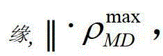
作为简单的估计,最大MD密度
其中l是TD的滑移长度,ρTD是预先存在的TD密度。在不存在任何交叉MD或其它滑移障碍下,l应当对应于投影滑移方向上的晶片尺寸,其对于基础滑移应当对应于(0001)c-平面104和生长平面106的交叉。通常,半极性GaN基底102是从c-平面GaN晶锭的横切,并且通常的晶片尺寸是在1cm×1cm的数量级。因此,


本发明注意到,MD密度,及因此的应力松弛,与TDs的运行长度具有直接的依赖关系。这使得本发明能够通过限制TDs的运行/滑移长度限制应力松弛。实现此的便利方式是图案化基底/外延层上的“台面”。这图解在图2(a)和2(b)(再次针对(11-22)的实例情况),其中台面200a、200b和200c被图案化到(11-22)GaN基底202的表面以形成基底202的图案化表面204。在图2(a)-(b)中,l1、l2和l3是对于图2(a)和2(b)中描绘的3个台面200a、200b和200c各个台面平行于TD滑移方向(m-轴[1-100],与MD线方向相同)的台面尺寸。还显示了台面200a-200c的高度h(~0.5微米),沿TD滑移方向的方向(与同样显示的[1-100]m-轴方向平行(||))具有长度L(~1厘米)的基底202的表面积,和[-1-123]方向(与c-轴的投影平行)。The present invention notes that MD density, and thus stress relaxation, has a direct dependence on the run length of TDs. This enables the present invention to limit stress relaxation by limiting the run/slip length of TDs. A convenient way to achieve this is to pattern the "mesas" on the substrate/epitaxial layer. This is illustrated in Figures 2(a) and 2(b) (again for the example case of (11-22)), where
通过利用在TD滑移方向的~10μm至~1mm的台面尺寸,TD滑移长度和MD密度可减少~103至~10倍,因此,通过TD滑移仅可实现非常小的失配减轻。这使得本发明能够生长具有更高合金组成和/或更大厚度的应变外延层,而在失配异质界面不产生高密度的MD(由于预先存在的TD,MD密度将被限于
图3是略述涉及本发明的一个实施方式的步骤的流程图。Figure 3 is a flowchart outlining the steps involved in one embodiment of the present invention.
本发明起始于半极性III-氮化物基底或外延层(生长在基底上),如方框300所示。基底/外延层的预先存在的TD密度将通常在105-107cm-2范围内。The invention starts with a semipolar Ill-nitride substrate or epitaxial layer (grown on the substrate), as shown at
方框302表示台面图案化,其中基底/外延层然后利用常规的平面印刷技术覆盖以具有期望台面图案的合适掩模(或光刻胶或介电)。尽管台面/掩模图案可采用任意形状,但重要的尺寸是与滑移方向平行的图案的尺寸(等式1中的l),因为它决定了最大MD密度(由于预先存在的TDs)。本发明不限于利用光刻胶或介电掩模图案化(也可采用其他方法)。
方框304表示台面蚀刻,其中基底/外延层然后被蚀刻成合适的深度(>50nm,例如0.1-10μm为通常的蚀刻深度)以形成台面结构,并且随后去除掩模(方框306)。蚀刻可包括但不限于湿或干蚀刻。
在装置外延结构的外延再生长(方框310)之前,台面侧壁和区域可任选地被覆盖以电介质,暴露的基底/外延层然后可经历离位或原位清洁或制备,如方框308所示。Prior to epitaxial regrowth of the device epitaxial structure (block 310), the mesa sidewalls and regions can optionally be covered with a dielectric, and the exposed substrate/epi layer can then undergo ex-situ or in-situ cleaning or preparation, as in
图4图解基底或外延层402上的III-氮化物异质结构400,其中
图5图解通过非极性基底502或外延层的基底图案化限制非极性III-氮化物异质结构(包括异质结构层500)中的应变松弛。还显示了MDs,III-氮化物的c-方向504,异质结构层500的生长方向506,和III-氮化物的m-或a-方向508。具有106cm-2TDs的l=1cm宽的晶片或基底502,利用关系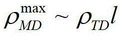
装置实施方式Device implementation
图1(a)-(b)、图2(a)-(b)、图5和图6图解各种装置实施方式。Figures 1(a)-(b), Figures 2(a)-(b), Figures 5 and 6 illustrate various device embodiments.
图5图解具有106cm-2或更大的穿透位错密度的半极性或非极性III-氮化物基底502或外延层;以及半极性或非极性III-氮化物基底502或外延层上(例如共格和/或异质外延地)生长的一个或多个半极性或非极性III-氮化物层500a、500b,诸如装置层(或异质结构500,包括半极性或非极性III-氮化物层或装置层500a、500b),其中异质结构500或层500a、500b具有104cm-2或更小的失配位错密度。5 illustrates a semipolar or nonpolar III-
基底502、202可以是整块III-氮化物或III-氮化物膜。基底可包括基底上生长(例如外来基底诸如蓝宝石、尖晶石或碳化硅上异质外延地)的初始半极性III-氮化物(例如模板)层或外延层502、202。The
图2(a)、图2(b)和图5图解了半极性或非极性III-氮化物基底202、502或外延层可包括沿穿透位错滑移的方向具有尺寸l的一个或多个台面200a,因此形成半极性或非极性III-氮化物基底或外延层502、202的图案化表面204(基底的表面204包括台面200a-c)。异质结构500或层500a-b异质外延地和/或共格地生长在图案化表面204上。Figures 2(a), 2(b) and 5 illustrate that a semi-polar or non-polar III-
穿透位错滑移通常由非极性或半极性III-氮化物基底102或外延层的非图案化表面110上异质外延地和共格地沉积的异质结构的非极性或半极性III-氮化物层100产生(参见图1)。图案化表面204的使用可降低或消除穿透位错滑移的量。Threading dislocation slip typically results from nonpolar or semipolar heterostructures deposited heteroepitaxially and coherently on non-patterned surfaces 110 of nonpolar or semipolar III-nitride substrates 102 or epitaxial layers. A polar III-nitride layer 100 is created (see FIG. 1 ). The use of patterned
尺寸l可以但不限于在10微米和1毫米之间。台面200a可具有各种形状,包括但不限于正方形或矩形(从顶上看)。Dimension l can be, but is not limited to, between 10 microns and 1 mm. The
层500a-b的至少一个可具有与非极性或半极性III-氮化物基底502或外延层不同的III-氮化物组成。At least one of the layers 500a-b may have a different Ill-nitride composition than the non-polar or semi-polar Ill-
异质结构500或层500a-b与图案化表面204之间的异质界面510可包括,与由在非极性或半极性III-氮化物基底或外延层102的非图案化表面110上异质外延地和/或共格地生长的半极性或非极性III-氮化物异质结构100所产生的失配位错密度相比,降低至少10倍或至少1000倍的失配位错(MD)密度。The
图6图解装置结构600,其包括可在图案化表面204上沉积的装置层,其中装置结构600或装置层是针对非极性或半极性III-氮化物发光二级管(LED)或发光的激光二级管(LD)。装置结构600包括异质结构500、或层500a-b、或一个或多个活性层602,其发射在与绿光波长或更长(例如黄或红光)的波长相应的一个或多个波长处具有峰值强度的光,或者在500nm或更长的波长处具有峰值强度的光。异质结构500的层500a-b可以是活性层602。6 illustrates a
本发明不限于在特定波长发射的装置,并且装置可在其它波长发射。装置可以是例如蓝、黄或红光发射装置。The invention is not limited to devices emitting at a particular wavelength, and devices may emit at other wavelengths. The device may be, for example, a blue, yellow or red light emitting device.
活性层602可包括一个或多个含铟的非极性或半极性III-氮化物层。非极性或半极性III-氮化物装置层500a-b或活性层602可足够厚,并且具有足够高的铟组成,以便发光装置发射具有期望波长的光。发光活性层(一个或多个)602可包括InGaN层,例如,一个或多个具有GaN阻挡层的InGaN量子阱。例如,InGaN量子阱可具有至少7%、至少10%、至少16%或至少30%的铟组成,以及大于4纳米(例如,5nm)、至少5nm或至少8nm的厚度。然而,量子阱厚度也可小于4nm,尽管它通常厚度的大于2nm。
半极性或非极性发光装置结构600的半极性或非极性III-氮化物装置层可进一步包括n-型波导层604a和p-型波导层604b和/或n-型包覆层606a和p-型包覆层606b,其足够厚,并且具有一定组成,以发挥作为LD或LED的活性层602所发出的光的波导/包覆层的功能。波导层604a-b可包括例如至少7%或至少30%的铟组成。The semipolar or nonpolar III-nitride device layer of the semipolar or nonpolar light emitting
波导层604a、604b可包括一个或多个具有GaN阻挡层的InGaN量子阱,包覆层606a、606b可包括例如一个或多个循环的交替AlGaN和GaN层。装置结构可无AlGaN包覆层。The
装置结构600可进一步包括AlGaN阻挡层608和GaN层610。尽管图6图解激光二级结构,但是该结构可根据需要进行改进以形成发光二级管结构。The
一个或多个III-氮化物半极性或非极性装置层500a-b可以是与另一半极性或非极性III-氮化物装置层或基底晶格失配、和/或具有与其不同的组成的异质结构或层。例如,装置层可以是GaN基底上的(Al,In)GaN层。例如,装置层可以是InGaN层(一个或多个)和AlGaN层(一个或多个),其中异质界面在InGaN层和AlGaN层、InGaN层和GaN层或AlGaN层和GaN层之间。One or more III-nitride semipolar or nonpolar device layers 500a-b may be lattice mismatched and/or have a different composition of heterogeneous structures or layers. For example, the device layer may be a (Al,In)GaN layer on a GaN substrate. For example, the device layer may be an InGaN layer(s) and an AlGaN layer(s), with a heterointerface between the InGaN layer and the AlGaN layer, the InGaN layer and the GaN layer, or the AlGaN layer and the GaN layer.
一个或多个半极性或半极性III-氮化物装置层500a、500b可具有与其在非极性或半极性III-氮化物基底102的非图案化表面110上的临界厚度相等或更大的厚度。One or more semipolar or semipolar III-nitride device layers 500a, 500b may have a critical thickness equal to or greater than its critical thickness on the non-patterned surface 110 of the nonpolar or semipolar III-nitride substrate 102. Great thickness.
平衡临界厚度对应于当它在能量方面有利于在层/基底界面上形成一个失配位错时的情况。The equilibrium critical thickness corresponds to the situation when it is energetically favorable to form one misfit dislocation at the layer/substrate interface.
实验或动力学临界厚度总是比平衡临界厚度稍微地或明显大。然而,不论临界厚度是否是平衡或动力学临界厚度,临界厚度对应于层从完全共格转变至部分松弛的情况下的厚度。The experimental or kinetic critical thickness is always slightly or significantly greater than the equilibrium critical thickness. However, regardless of whether the critical thickness is an equilibrium or a kinetic critical thickness, the critical thickness corresponds to the thickness at which the layer transitions from fully coherent to partially relaxed.
临界厚度的另一实例是Matthews Blakeslee临界厚度[4]。Another example of a critical thickness is the Matthews Blakeslee critical thickness [4].
例如,所有活性层600的总厚度612(例如,多量子阱堆叠厚度)可等于或大于非图案化表面110上活性层的临界厚度。n-型或p-型波导层604a、604b的总厚度614可等于或大于非图案化表面110上波导层604a、604b的临界厚度。n-型或p-型包覆层606a、606b的总厚度616可等于或大于非图案表面110上包覆层606a、606b的临界厚度。For example, the total thickness 612 (eg, multiple quantum well stack thickness) of all
然而,利用图案化表面204,层602、604a、604b和606b、606a可共格生长。对于在层Y上生长的层X,对于共格生长的情况,X的平面内晶格常数(一个或多个)被限于与下层Y相同。如果X完全松弛,那么X的晶格常数假定是其固有(在不存在任何应变下)值。如果X关于Y既不共格也不完全松弛,那么它被认为是部分松弛的。在一些情况下,基底可具有一些残余应变。However, with the patterned
采用该方法的装置结构可由于更宽的可利用装置设计空间的可能而不同(例如,具有更高组成/更厚合金层的无缺陷共格结构)。Device structures employing this approach may differ due to the possibility of a wider available device design space (eg, defect-free coherent structures with higher composition/thicker alloy layers).
一个或多个装置层500a-b可具有足够高的厚度和/或组成,以使膜,包括所有的或一个或多个装置层500a-b,具有与对于非图案化基底上的松弛而言的膜临界厚度相近或更大的厚度。The one or more device layers 500a-b can have a thickness and/or composition high enough that the film, including all or one or more of the device layers 500a-b, has a thickness comparable to that for relaxation on a non-patterned substrate. The thickness of the film is similar to or greater than the critical thickness.
一个或多个半极性或非极性III-氮化物装置层500a、500b,与在半极性或非极性III-氮化物基底或外延层的非图案化或不同图案化表面上生长的半极性或非极性III-氮化物装置层相比,可以更厚,且具有更高的合金组成(例如更多的Al、In和/或B、或非镓元素)。One or more semipolar or nonpolar III-nitride device layers 500a, 500b, grown on non-patterned or differently patterned surfaces of semipolar or nonpolar III-nitride substrates or epitaxial layers Semi-polar or non-polar Ill-nitride device layers can be thicker and have a higher alloy composition (eg, more Al, In, and/or B, or non-Gallium elements) than semi-polar or non-polar III-nitride device layers.
因此,本发明的一个或多个实施方式阐明限制在III-氮化物基底或外延层上生长的异质外延III-氮化物层500的应变松弛的方法,包括图案化基底或外延层;和在图案化基底202上生长III-氮化物层500。Accordingly, one or more embodiments of the present invention set forth methods of limiting strain relaxation of a heteroepitaxial III-
本发明的实施方式包括在图案化表面204上生长、处理和/或接触装置层500a、500b以制造任何电子或光电子装置,包括但不限于LED、晶体管、太阳能电池或LD。Embodiments of the invention include growing, processing and/or contacting device layers 500a, 500b on patterned
可能的改进possible improvements
基底/外延层可采用可选的技术生长,例如氢化物蒸汽相外延(HVPE)/分子束外延(MBE)/化学蒸汽沉积(CVD)/金属有机蒸汽沉积(MOCVD)/氨热技术等。图案化蚀刻台面的工艺流程可以不同——例如,正/负光刻胶、各种介电掩模(SiO2、硅氮化物等)可用于蚀刻(例如,干/湿蚀刻)。The substrate/epi layer can be grown using alternative techniques such as hydride vapor phase epitaxy (HVPE)/molecular beam epitaxy (MBE)/chemical vapor deposition (CVD)/metal organic vapor deposition (MOCVD)/ammonothermal techniques, etc. The process flow for patterning etch mesas can be different - eg positive/negative photoresist, various dielectric masks ( SiO2 , silicon nitride, etc.) can be used for etching (eg dry/wet etch).
能够可选地使用各种蚀刻技术和/或清洁程序。装置外延再生长可利用各种生长技术/其组合进行——例如,HVPE、MBE、CVD、MOCVD或氨热生长等。此外,如果MDs通过棱锥/棱柱滑移形成,那么MDs的线方向将以此改变,所以台面尺寸将必须因此而更改。在所有情况中,l(等式1中)对应于滑移方向中的TD运行长度,并且是重要的尺寸。Various etching techniques and/or cleaning procedures can optionally be used. Device epitaxial regrowth can be performed using various growth techniques/combinations thereof - for example, HVPE, MBE, CVD, MOCVD, or ammonothermal growth, among others. Furthermore, if MDs are formed by pyramid/prism slip, then the line direction of the MDs will change accordingly, so the mesa dimensions will have to change accordingly. In all cases, l (in Equation 1) corresponds to the TD run length in the slip direction and is the important dimension.
优势和改进Advantages and Improvements
本发明可适用于在III-氮化物基底上生长的电子和光电子装置(例如,LEDs、LDs、太阳能电池、高电子迁移率晶体管(HEMTs)等)。The present invention is applicable to electronic and optoelectronic devices (eg, LEDs, LDs, solar cells, high electron mobility transistors (HEMTs), etc.) grown on III-nitride substrates.
本发明提供限制半极性III-氮化物异质外延中的应力松弛的方法,因此提供混合有较厚/较高组成合金外延层的伸长装置设计空间。对于LEDs或LDs,可获得加宽的发射波长,例如可获得绿、黄和红LEDs和LDs。对于LDs,通过使用较厚/较高组成波导和包覆层可获得明显改进的光学波导。The present invention provides a way to limit stress relaxation in semipolar Ill-nitride heteroepitaxial, thus providing design space for elongated devices mixed with thicker/higher composition alloy epilayers. For LEDs or LDs, broadened emission wavelengths are available, for example green, yellow and red LEDs and LDs are available. For LDs, significantly improved optical waveguides can be obtained by using thicker/higher composition waveguides and cladding layers.
现有技术的半极性III-氮化物装置在如此得到的GaN基底上生长(通常通过HVPE生长,TD密度~106cm-2)。如上所讨论,这暗示着有足够的预先存在的TDs以减轻~2%的失配应力。可选地,看等式1,MD密度也可通过减少TD密度来限制。事实上,已经报道了通过氨热法生长的GaN基底的TD密度为5×104cm-2。然而,这样的基底并不容易获得,TD密度强烈地依赖于生长技术和生长条件。商业可得的HVPE生长的GaN基底通常具有的TD密度为~106cm-2。相反,本发明可适用于具有可变程度的TD密度的基底/外延层,并且因此不受预先存在的TD密度的限制。因此,本发明具有较少的约束条件并且应用广泛。State-of-the-art semi-polar III-nitride devices are grown on the thus obtained GaN substrates (typically grown by HVPE, TD density ~10 6 cm −2 ). As discussed above, this implies that there are enough pre-existing TDs to relieve the ~2% mismatch stress. Alternatively, see
参考文献references
下列参考文献通过引用并入本文。The following references are incorporated herein by reference.
[1]Tyagi et al.,Applied Physics Letters95,251905(2009).[1]Tyagi et al., Applied Physics Letters 95, 251905(2009).
[2]Young et al.,Applied Physics Express3,011004(2010).[2]Young et al., Applied Physics Express3, 011004(2010).
[3]Kucharski et al.,Applied Physics Letters95,131119(2009).[3]Kucharski et al.,Applied Physics Letters95,131119(2009).
[4]J.Matthews and A.Blakeslee,J.Cryst.Growth32265(1976).[4] J. Matthews and A. Blakeslee, J. Cryst. Growth 32265 (1976).
结论in conclusion
这结束了本发明的优选实施方式的描述。本发明一个或多个实施方式的前述描述已经呈现用于阐明和描述的目的。它没有意图是穷尽性的或者限制本发明为所公开的具体形式。鉴于上述教导许多改进和改变是可能的。本发明的范围意图不受该详述的限制,而是受所附权利要求的限制。This concludes the description of the preferred embodiment of the invention. The foregoing description of one or more embodiments of the invention has been presented for purposes of illustration and description. It is not intended to be exhaustive or to limit the invention to the precise form disclosed. Many modifications and variations are possible in light of the above teachings. It is intended that the scope of the invention be limited not by this detailed description, but rather by the claims appended hereto.
Claims (25)
Applications Claiming Priority (3)
| Application Number | Priority Date | Filing Date | Title |
|---|---|---|---|
| US40687610P | 2010-10-26 | 2010-10-26 | |
| US61/406,876 | 2010-10-26 | ||
| PCT/US2011/057811 WO2012058264A1 (en) | 2010-10-26 | 2011-10-26 | Limiting strain relaxation in iii-nitride heterostructures by substrate and epitaxial layer patterning |
Publications (1)
| Publication Number | Publication Date |
|---|---|
| CN103190041A true CN103190041A (en) | 2013-07-03 |
Family
ID=45972188
Family Applications (1)
| Application Number | Title | Priority Date | Filing Date |
|---|---|---|---|
| CN2011800518424A Pending CN103190041A (en) | 2010-10-26 | 2011-10-26 | Confining strain relaxation in III-nitride heterostructures by substrate and epilayer patterning |
Country Status (7)
| Country | Link |
|---|---|
| US (1) | US8853669B2 (en) |
| EP (1) | EP2633592A1 (en) |
| JP (1) | JP2013544027A (en) |
| KR (1) | KR20130141546A (en) |
| CN (1) | CN103190041A (en) |
| TW (1) | TW201222872A (en) |
| WO (1) | WO2012058264A1 (en) |
Cited By (2)
| Publication number | Priority date | Publication date | Assignee | Title |
|---|---|---|---|---|
| CN107615602A (en) * | 2015-06-08 | 2018-01-19 | 松下知识产权经营株式会社 | Light-emitting component |
| CN113287205A (en) * | 2018-10-31 | 2021-08-20 | 加利福尼亚大学董事会 | Method for obtaining smooth surfaces by epitaxial lateral overgrowth |
Families Citing this family (12)
| Publication number | Priority date | Publication date | Assignee | Title |
|---|---|---|---|---|
| JP5972798B2 (en) * | 2010-03-04 | 2016-08-17 | ザ リージェンツ オブ ザ ユニバーシティ オブ カリフォルニア | Semipolar III-nitride optoelectronic device on M-plane substrate with miscut less than +/− 15 degrees in C direction |
| US8358673B2 (en) * | 2011-02-17 | 2013-01-22 | Corning Incorporated | Strain balanced laser diode |
| US9153483B2 (en) | 2013-10-30 | 2015-10-06 | Taiwan Semiconductor Manufacturing Company, Ltd. | Method of semiconductor integrated circuit fabrication |
| KR101594171B1 (en) * | 2014-06-16 | 2016-02-16 | (재)한국나노기술원 | method for avoiding crack of epi-film grown on semiconductor substrate and manufacturing method of semiconductor devices thereby |
| US20170236807A1 (en) * | 2014-10-28 | 2017-08-17 | The Regents Of The University Of California | Iii-v micro-led arrays and methods for preparing the same |
| WO2016069766A1 (en) * | 2014-10-28 | 2016-05-06 | The Regents Of The University Of California | Flexible arrays of micro light emitting diodes using a photoelectrochemical (pec) liftoff technique |
| TWI568014B (en) * | 2015-10-07 | 2017-01-21 | 財團法人工業技術研究院 | Three or five nitride semiconductor components |
| WO2020017207A1 (en) * | 2018-07-20 | 2020-01-23 | ソニーセミコンダクタソリューションズ株式会社 | Semiconductor light emitting element |
| CN109873299B (en) * | 2019-02-14 | 2020-02-21 | 中国科学院半导体研究所 | GaN-based multi-quantum well laser epitaxial wafer with low V-type defect density and preparation method |
| US11522077B2 (en) | 2020-05-27 | 2022-12-06 | Taiwan Semiconductor Manufacturing Company, Ltd. | Integration of p-channel and n-channel E-FET III-V devices with optimization of device performance |
| JP7589940B2 (en) * | 2021-03-25 | 2024-11-26 | 旭化成株式会社 | Laser diode manufacturing method and laser diode |
| WO2023176260A1 (en) * | 2022-03-15 | 2023-09-21 | ヌヴォトンテクノロジージャパン株式会社 | Semiconductor device and production method for semiconductor device |
Citations (7)
| Publication number | Priority date | Publication date | Assignee | Title |
|---|---|---|---|---|
| US20030102469A1 (en) * | 2001-11-30 | 2003-06-05 | Jones Robert E. | Semiconductor device and method therefor |
| US20040079969A1 (en) * | 2000-03-27 | 2004-04-29 | Yasunobu Umemoto | Semiconductor integrated circuit making use of standard cells |
| CN1571175A (en) * | 2003-07-16 | 2005-01-26 | 璨圆光电股份有限公司 | Selectively grown LED structures |
| CN101307498A (en) * | 2000-03-13 | 2008-11-19 | 克利公司 | Iii-v nitride substrate wafer and its manufacture method and uses |
| CN101420003A (en) * | 2007-10-24 | 2009-04-29 | 泰谷光电科技股份有限公司 | Structure of light emitting diode and manufacturing method thereof |
| WO2010041657A1 (en) * | 2008-10-07 | 2010-04-15 | 住友電気工業株式会社 | Gallium nitride semiconductor light-emitting element and method for producing the same, gallium nitride light-emitting diode, epitaxial wafer, and method for producing gallium nitride light-emitting diode |
| US20100264460A1 (en) * | 2007-01-26 | 2010-10-21 | Grandusky James R | Thick pseudomorphic nitride epitaxial layers |
Family Cites Families (8)
| Publication number | Priority date | Publication date | Assignee | Title |
|---|---|---|---|---|
| US6165874A (en) | 1997-07-03 | 2000-12-26 | The United States Of America As Represented By The Administrator Of The National Aeronautics And Space Administration | Method for growth of crystal surfaces and growth of heteroepitaxial single crystal films thereon |
| US7034330B2 (en) * | 2002-10-22 | 2006-04-25 | Showa Denko Kabushiki Kaisha | Group-III nitride semiconductor device, production method thereof and light-emitting diode |
| US7323256B2 (en) | 2003-11-13 | 2008-01-29 | Cree, Inc. | Large area, uniformly low dislocation density GaN substrate and process for making the same |
| JP4390007B2 (en) | 2008-04-07 | 2009-12-24 | 住友電気工業株式会社 | Group III nitride semiconductor device and epitaxial wafer |
| CN102449737A (en) | 2009-03-02 | 2012-05-09 | 加利福尼亚大学董事会 | Devices grown on nonpolar or semipolar (Ga, Al, In, B) N substrates |
| US8189639B2 (en) | 2010-05-28 | 2012-05-29 | Corning Incorporated | GaN-based laser diodes with misfit dislocations displaced from the active region |
| US8729559B2 (en) * | 2010-10-13 | 2014-05-20 | Soraa, Inc. | Method of making bulk InGaN substrates and devices thereon |
| US20120100650A1 (en) | 2010-10-26 | 2012-04-26 | The Regents Of The University Of California | Vicinal semipolar iii-nitride substrates to compensate tilt of relaxed hetero-epitaxial layers |
-
2011
- 2011-10-26 CN CN2011800518424A patent/CN103190041A/en active Pending
- 2011-10-26 US US13/281,775 patent/US8853669B2/en active Active
- 2011-10-26 KR KR1020137013226A patent/KR20130141546A/en not_active Withdrawn
- 2011-10-26 EP EP11836982.6A patent/EP2633592A1/en not_active Withdrawn
- 2011-10-26 JP JP2013536768A patent/JP2013544027A/en active Pending
- 2011-10-26 TW TW100138950A patent/TW201222872A/en unknown
- 2011-10-26 WO PCT/US2011/057811 patent/WO2012058264A1/en not_active Ceased
Patent Citations (7)
| Publication number | Priority date | Publication date | Assignee | Title |
|---|---|---|---|---|
| CN101307498A (en) * | 2000-03-13 | 2008-11-19 | 克利公司 | Iii-v nitride substrate wafer and its manufacture method and uses |
| US20040079969A1 (en) * | 2000-03-27 | 2004-04-29 | Yasunobu Umemoto | Semiconductor integrated circuit making use of standard cells |
| US20030102469A1 (en) * | 2001-11-30 | 2003-06-05 | Jones Robert E. | Semiconductor device and method therefor |
| CN1571175A (en) * | 2003-07-16 | 2005-01-26 | 璨圆光电股份有限公司 | Selectively grown LED structures |
| US20100264460A1 (en) * | 2007-01-26 | 2010-10-21 | Grandusky James R | Thick pseudomorphic nitride epitaxial layers |
| CN101420003A (en) * | 2007-10-24 | 2009-04-29 | 泰谷光电科技股份有限公司 | Structure of light emitting diode and manufacturing method thereof |
| WO2010041657A1 (en) * | 2008-10-07 | 2010-04-15 | 住友電気工業株式会社 | Gallium nitride semiconductor light-emitting element and method for producing the same, gallium nitride light-emitting diode, epitaxial wafer, and method for producing gallium nitride light-emitting diode |
Cited By (3)
| Publication number | Priority date | Publication date | Assignee | Title |
|---|---|---|---|---|
| CN107615602A (en) * | 2015-06-08 | 2018-01-19 | 松下知识产权经营株式会社 | Light-emitting component |
| CN107615602B (en) * | 2015-06-08 | 2020-05-01 | 松下知识产权经营株式会社 | Light emitting element |
| CN113287205A (en) * | 2018-10-31 | 2021-08-20 | 加利福尼亚大学董事会 | Method for obtaining smooth surfaces by epitaxial lateral overgrowth |
Also Published As
| Publication number | Publication date |
|---|---|
| JP2013544027A (en) | 2013-12-09 |
| US20120097919A1 (en) | 2012-04-26 |
| WO2012058264A1 (en) | 2012-05-03 |
| KR20130141546A (en) | 2013-12-26 |
| TW201222872A (en) | 2012-06-01 |
| US8853669B2 (en) | 2014-10-07 |
| EP2633592A1 (en) | 2013-09-04 |
Similar Documents
| Publication | Publication Date | Title |
|---|---|---|
| US8853669B2 (en) | Limiting strain relaxation in III-nitride hetero-structures by substrate and epitaxial layer patterning | |
| US8203159B2 (en) | Method for growth of semipolar (Al,In,Ga,B)N optoelectronic devices | |
| CN106972346B (en) | Semipolar III-nitride optoelectronic devices on m-plane substrates with miscut in the C-direction of less than +/-15degrees | |
| US8481991B2 (en) | Anisotropic strain control in semipolar nitride quantum wells by partially or fully relaxed aluminum indium gallium nitride layers with misfit dislocations | |
| US8247249B2 (en) | Semi-polar nitride-based light emitting structure and method of forming same | |
| CN102484142A (en) | Anisotropic strain control in semipolar nitride quantum wells by partially or fully relaxed aluminum indium gallium nitride layers with misfit dislocations | |
| WO2010051537A1 (en) | Optoelectronic device based on non-polar and semi-polar aluminum indium nitride and aluminum indium gallium nitride alloys | |
| JP4696285B2 (en) | R-plane sapphire substrate, epitaxial substrate and semiconductor device using the same, and manufacturing method thereof | |
| US9324913B2 (en) | Nitride semiconductor structure, multilayer structure, and nitride semiconductor light-emitting element | |
| US20120100650A1 (en) | Vicinal semipolar iii-nitride substrates to compensate tilt of relaxed hetero-epitaxial layers | |
| KR20090023672A (en) | Nano-based semiconductor device | |
| JP2010510655A (en) | Light emitting diode and laser diode using N-plane GaN, InN and AlN and their alloys | |
| CN103890243A (en) | Suppression of relaxation by limited area epitaxy on non-c-plane (in,al,b,ga)n | |
| KR101068865B1 (en) | Nitride semiconductor growth substrate and light emitting device using the same | |
| JP5557180B2 (en) | Manufacturing method of semiconductor light emitting device | |
| JP2001308464A (en) | Nitride semiconductor element, method for manufacturing nitride semiconductor crystal, and nitride semiconductor substrate | |
| JP4517770B2 (en) | Nitride semiconductor device | |
| KR101250475B1 (en) | Heterogeneous substrate having insulating material pattern and nitride-based semiconductor device using the same | |
| JP2001274517A (en) | Substrate for semiconductor element, method for manufacturing the same and semiconductor element using the substrate for semiconductor element |
Legal Events
| Date | Code | Title | Description |
|---|---|---|---|
| C06 | Publication | ||
| PB01 | Publication | ||
| C10 | Entry into substantive examination | ||
| SE01 | Entry into force of request for substantive examination | ||
| C05 | Deemed withdrawal (patent law before 1993) | ||
| WD01 | Invention patent application deemed withdrawn after publication |
Application publication date: 20130703 |