CN103178062A - Metal nanocrystalline storage - Google Patents
Metal nanocrystalline storage Download PDFInfo
- Publication number
- CN103178062A CN103178062A CN2011104296082A CN201110429608A CN103178062A CN 103178062 A CN103178062 A CN 103178062A CN 2011104296082 A CN2011104296082 A CN 2011104296082A CN 201110429608 A CN201110429608 A CN 201110429608A CN 103178062 A CN103178062 A CN 103178062A
- Authority
- CN
- China
- Prior art keywords
- metal
- layer
- metal nanocrystal
- nanocrystal
- memory according
- Prior art date
- Legal status (The legal status is an assumption and is not a legal conclusion. Google has not performed a legal analysis and makes no representation as to the accuracy of the status listed.)
- Pending
Links
Images


Landscapes
- Semiconductor Memories (AREA)
- Non-Volatile Memory (AREA)
Abstract
本发明公开了一种金属纳米晶存储器。该金属纳米晶存储器包括:衬底;形成于衬底沟道区两侧的源端和漏端;及依次形成于衬底沟道区上方的隧穿介质层、金属纳米晶存储层、电荷阻挡层和栅电极;其中,该金属纳米晶存储层是由金属纳米晶胶体经喷涂方法沉积于隧穿介质层并蒸发金属纳米晶胶体内的溶剂而形成的。本发明金属纳米晶存储器,是基于激光烧蚀、喷枪喷涂的方法来实现,与常规的制备纳米晶浮栅非挥发性存储器比较,具有成本低廉、纳米颗粒直径可控,均匀性好,无污染、器件性能优良等诸多优点。
The invention discloses a metal nanocrystal memory. The metal nanocrystal memory comprises: a substrate; source terminals and drain terminals formed on both sides of the substrate channel region; layer and gate electrode; wherein, the metal nanocrystal storage layer is formed by depositing metal nanocrystal colloid on the tunnel dielectric layer by spraying method and evaporating the solvent in the metal nanocrystal colloid. The metal nanocrystalline memory of the present invention is realized based on the method of laser ablation and spray gun spraying. Compared with the conventional preparation of nanocrystalline floating gate non-volatile memory, it has the advantages of low cost, controllable nanoparticle diameter, good uniformity and no pollution. , Excellent device performance and many other advantages.
Description
技术领域 technical field
本发明涉及微电子行业存储器技术领域,尤其涉及一种金属纳米晶存储器。The invention relates to the technical field of memory in the microelectronics industry, in particular to a metal nanocrystal memory.
背景技术 Background technique
目前的微电子产品主要分为逻辑器件与存储器件两大类,存储器件在微电子领域占有非常重要的地位。存储器件一般可分为挥发性存储器与非挥发存储器。非挥发性存储器的主要特点是在不加电的情况下也能够长期保持存储的信息。它既有只读存储器的特点,又有很高的存取速度,而且易于擦除和重写,功耗较小。随着多媒体应用、移动通信等对大容量、低功耗存储的需要,非挥发性存储器,特别是闪速存储器(Flash),所占半导体器件的市场份额变得越来越大,也越来越成为一种相当重要的存储器类型。对于这些存储器,如何通过调整结构材料来提高性能和简化工艺,有效地控制工艺成本是急待解决的问题。以纳米晶存储器为代表的Flash存储器即具有这方面的优势。The current microelectronics products are mainly divided into two categories: logic devices and storage devices, and storage devices occupy a very important position in the field of microelectronics. Storage devices can generally be classified into volatile memories and non-volatile memories. The main feature of non-volatile memory is the ability to retain stored information for a long period of time without power on. It not only has the characteristics of read-only memory, but also has high access speed, and is easy to erase and rewrite, and consumes less power. With the demand for large-capacity and low-power storage in multimedia applications and mobile communications, the market share of non-volatile memory, especially flash memory (Flash), is becoming larger and larger, and is also increasing. The more it becomes a very important memory type. For these memories, how to improve the performance and simplify the process by adjusting the structural materials, and effectively control the process cost is an urgent problem to be solved. Flash memory represented by nanocrystalline memory has advantages in this regard.
传统Flash存储器的组成核心,是基于多晶硅薄膜浮栅结构的硅基非挥发性存储器。但多晶硅薄膜浮栅器件具有制造工艺较复杂、写入时间长、写入功耗较大等缺点。而且随着技术节点的不断降低,器件隧穿介质层也越来越薄,这使得器件的电荷泄露问题日趋严重。这是因为对于传统的多晶硅薄膜浮栅结构存储器,隧穿氧化层上的一处缺陷即会形成致命的放电通道使器件失效。为了解决这个问题,电荷俘获型存储器被提出来。利用俘获层中电荷局域化存储的特性,电荷俘获型存储器实现分立电荷存储,隧穿介质层上的缺陷只会造成局部的电荷泄漏,这样使电荷保持更加稳定。其中纳米晶存储器由于具备使用更薄隧穿氧化层,更低的编程/擦除(P/E)电压、更快的P/E速度、更强的数据保持特性(retention)等的优势引起了科学界,产业界的极大关注。同时引入高K材料作为隧穿介质层和电荷阻挡层可以有效的解决数据保持和高擦写的折中问题。因为采用高K栅介质,在保证单位栅电容不变条件下,栅介质层的物理厚度将高于传统材料(如二氧化硅,氮化硅)的物理厚度,从而可有效解决栅泄漏电流问题并保持高的编程擦除速度。采用纳米晶材料的陷阱俘获存储器可以满足高性能存储器的需求,得到了广泛的研究。同时,金属纳米晶与Si或Ge纳米晶相比,具有更大的优势,如功函数可调、在费米能级附近态密度很高、微扰小等因此受到了产业界和科研界的广泛关注。The core of traditional Flash memory is silicon-based non-volatile memory based on polysilicon thin film floating gate structure. However, polysilicon thin film floating gate devices have disadvantages such as complicated manufacturing process, long writing time, and high writing power consumption. Moreover, with the continuous reduction of technology nodes, the tunnel dielectric layer of devices is getting thinner and thinner, which makes the charge leakage problem of devices more and more serious. This is because for traditional polysilicon thin film floating gate memory, a defect on the tunnel oxide layer will form a fatal discharge channel and cause the device to fail. In order to solve this problem, a charge-trap memory is proposed. Using the characteristics of localized storage of charges in the trapping layer, the charge-trapping memory realizes discrete charge storage, and the defects on the tunneling dielectric layer only cause local charge leakage, which makes the charge more stable. Among them, nanocrystalline memory has attracted more attention due to its advantages of using a thinner tunnel oxide layer, lower program/erase (P/E) voltage, faster P/E speed, and stronger data retention. The scientific community and the industry are of great concern. At the same time, the introduction of high-K materials as the tunneling dielectric layer and the charge blocking layer can effectively solve the trade-off problem between data retention and high erasability. Because of the high-K gate dielectric, the physical thickness of the gate dielectric layer will be higher than that of traditional materials (such as silicon dioxide, silicon nitride) under the condition that the unit gate capacitance remains unchanged, which can effectively solve the problem of gate leakage current And maintain a high programming and erasing speed. Trap-trap memories using nanocrystalline materials can meet the needs of high-performance memories and have been extensively studied. At the same time, compared with Si or Ge nanocrystals, metal nanocrystals have greater advantages, such as adjustable work function, high density of states near the Fermi level, and small perturbation. Therefore, they are favored by the industry and scientific research circles. extensive attention.
制备纳米晶存储器,其中关键工艺是纳米晶薄膜的制备。其制备方法多种多样,主要包括以下几种:(1)离子注入的方法形成纳米晶颗粒;(2)快速热退火的方法形成纳米晶颗粒;(3)CVD直接生长的方法制备纳米晶颗粒。Preparation of nanocrystalline memory, wherein the key process is the preparation of nanocrystalline thin film. There are various preparation methods, mainly including the following: (1) ion implantation method to form nanocrystalline particles; (2) rapid thermal annealing method to form nanocrystalline particles; (3) CVD direct growth method to prepare nanocrystalline particles .
在实现本发明的过程中,申请人意识到现有技术金属纳米晶存储器件存在如下技术缺陷:金属纳米晶颗粒直径较大,均匀性差,严重影响浮栅存储器的存储性能。In the process of realizing the present invention, the applicant realized that the prior art metal nanocrystal storage device has the following technical defects: the metal nanocrystal particles have large diameter and poor uniformity, which seriously affects the storage performance of the floating gate memory.
发明内容 Contents of the invention
(一)要解决的技术问题(1) Technical problems to be solved
为解决上述的一个或多个问题,本发明提供了一种金属纳米晶存储器的制备方法,以提高金属纳米晶层的质量,降低制备金属纳米晶存储器的工艺复杂度和成本。In order to solve one or more of the above problems, the present invention provides a method for preparing a metal nanocrystal memory, so as to improve the quality of the metal nanocrystal layer and reduce the process complexity and cost of preparing the metal nanocrystal memory.
(二)技术方案(2) Technical solutions
根据本发明的一个方面,提供了一种金属纳米晶存储器。该金属纳米晶存储器包括:衬底;形成于衬底沟道区两侧的源端和漏端;及依次形成于衬底沟道区上方的隧穿介质层、金属纳米晶存储层、电荷阻挡层和栅电极;其中,该金属纳米晶存储层是由金属纳米晶胶体经喷涂方法沉积于隧穿介质层上并蒸发金属纳米晶胶体内的溶剂而形成的。According to one aspect of the present invention, a metal nanocrystal memory is provided. The metal nanocrystal memory includes: a substrate; source terminals and drain terminals formed on both sides of the substrate channel region; layer and gate electrode; wherein, the metal nanocrystal storage layer is formed by depositing metal nanocrystal colloid on the tunnel dielectric layer by spraying and evaporating the solvent in the metal nanocrystal colloid.
(三)有益效果(3) Beneficial effects
由上述技术方案可知,本发明金属纳米晶存储器具有以下有益效果:It can be seen from the above technical scheme that the metal nanocrystal memory of the present invention has the following beneficial effects:
(1)本发明纳米晶存储器综合了纳米晶的电荷局域化存储特性和高K栅介质的防泄漏特性;(1) The nanocrystalline memory of the present invention combines the charge localized storage characteristics of nanocrystals and the anti-leakage characteristics of high-K gate dielectrics;
(2)本发明金属纳米晶存储器,是基于激光烧蚀、喷枪喷涂的方法来实现,与常规的制备纳米晶浮栅非挥发性存储器比较,具有成本低廉、纳米颗粒直径可控,均匀性好,无污染、器件性能优良等诸多优点。(2) The metal nanocrystalline memory of the present invention is realized based on the method of laser ablation and spray gun spraying. Compared with the conventional preparation of nanocrystalline floating gate non-volatile memory, it has low cost, controllable nanoparticle diameter, and good uniformity. , No pollution, excellent device performance and many other advantages.
附图说明 Description of drawings
图1A为本发明实施例金属纳米晶存储器的剖面示意图;1A is a schematic cross-sectional view of a metal nanocrystal memory according to an embodiment of the present invention;
图1B为本发明实施例纳米晶存储器的三维结构示意图;1B is a schematic diagram of a three-dimensional structure of a nanocrystalline memory according to an embodiment of the present invention;
图2A为由本发明实施例纳米晶存储器构成的NOR型阵列的示意图;2A is a schematic diagram of a NOR array composed of nanocrystalline memory according to an embodiment of the present invention;
图2B为图2A所示NOR型阵列方向的示意图;Figure 2B is a schematic diagram of the direction of the NOR array shown in Figure 2A;
图3A为本发明实施例金属纳米晶存储器制备方法中对衬底进行浅沟隔离后沿A-A’方向的结构示意图;3A is a schematic structural diagram along the A-A' direction after the substrate is subjected to shallow trench isolation in the method for preparing a metal nanocrystal memory according to an embodiment of the present invention;
图3B为本发明实施例金属纳米晶存储器制备方法中对衬底进行浅沟隔离后沿B-B’方向的结构示意图;3B is a schematic structural view along the B-B' direction after the substrate is subjected to shallow trench isolation in the method for preparing a metal nanocrystal memory according to an embodiment of the present invention;
图4A为本发明实施例金属纳米晶存储器制备方法中淀积高K隧穿介质层后沿A-A’方向的结构示意图;4A is a schematic structural diagram along the A-A' direction after depositing a high-K tunnel dielectric layer in the method for preparing a metal nanocrystal memory according to an embodiment of the present invention;
图4B为本发明实施例金属纳米晶存储器制备方法中淀积高K隧穿介质层后沿B-B’方向的结构示意图;4B is a schematic structural view along the B-B' direction after depositing a high-K tunnel dielectric layer in the method for preparing a metal nanocrystal memory according to an embodiment of the present invention;
图5A为本发明实施例金属纳米晶存储器制备方法中激光烧蚀法制备金属纳米晶胶体装置的示意图;5A is a schematic diagram of a metal nanocrystal colloid device prepared by laser ablation in the method for preparing a metal nanocrystal memory according to an embodiment of the present invention;
图5B为本发明实施例金属纳米晶存储器制备方法中沉积金属纳米晶胶体所用喷枪的示意图;5B is a schematic diagram of a spray gun used for depositing a metal nanocrystal colloid in a method for preparing a metal nanocrystal memory according to an embodiment of the present invention;
图6A为本发明实施例金属纳米晶存储器制备方法中形成金属纳米晶存储层后沿A-A’方向的结构示意图;6A is a schematic structural diagram along the A-A' direction after forming a metal nanocrystal storage layer in the method for preparing a metal nanocrystal memory according to an embodiment of the present invention;
图6B为本发明实施例金属纳米晶存储器制备方法中形成金属纳米晶存储层后沿B-B’方向的结构示意图;6B is a schematic structural diagram along the B-B' direction after forming a metal nanocrystal storage layer in the method for preparing a metal nanocrystal memory according to an embodiment of the present invention;
图7A为本发明实施例金属纳米晶存储器制备方法中淀积电荷阻挡层后沿A-A’方向的结构示意图;7A is a schematic structural view along the A-A' direction after depositing a charge blocking layer in the method for preparing a metal nanocrystal memory according to an embodiment of the present invention;
图7B为本发明实施例金属纳米晶存储器制备方法中淀积电荷阻挡层后沿B-B’方向的结构示意图;7B is a schematic structural view along the B-B' direction after depositing a charge blocking layer in the method for preparing a metal nanocrystal memory according to an embodiment of the present invention;
图8为本发明实施例金属纳米晶存储器制备方法中A-A’方向经过刻蚀后的结构示意图;Fig. 8 is a schematic structural view of the A-A' direction after etching in the method for preparing a metal nanocrystal memory according to an embodiment of the present invention;
图9A为本发明实施例金属纳米晶存储器制备方法中沉积栅极后沿A-A’方向的结构示意图;9A is a schematic structural diagram along the A-A' direction after depositing a gate in the method for manufacturing a metal nanocrystal memory according to an embodiment of the present invention;
图9B为本发明实施例金属纳米晶存储器制备方法中沉积栅极后沿B-B’方向的结构示意图;9B is a schematic structural diagram along the B-B' direction after depositing the gate in the method for manufacturing the metal nanocrystal memory according to the embodiment of the present invention;
图10为本发明实施例金属纳米晶存储器制备方法中沿B-B’方向进行刻蚀后沿B-B’方向的结构示意图;Fig. 10 is a schematic structural diagram along the B-B' direction after etching along the B-B' direction in the method for preparing a metal nanocrystal memory according to an embodiment of the present invention;
图11为本发明实施例金属纳米晶存储器制备方法中形成源端和漏端后沿B-B’方向的结构示意图。Fig. 11 is a schematic diagram of the structure along the B-B' direction after the source terminal and the drain terminal are formed in the method for fabricating the metal nanocrystal memory according to the embodiment of the present invention.
具体实施方式 Detailed ways
为使本发明的目的、技术方案和优点更加清楚明白,以下结合具体实施例,并参照附图,对本发明进一步详细说明。虽然本文可提供包含特定值的参数的示范,但应了解,参数无需确切等于相应的值,而是可在可接受的误差容限或设计约束内近似于所述值。In order to make the object, technical solution and advantages of the present invention clearer, the present invention will be described in further detail below in conjunction with specific embodiments and with reference to the accompanying drawings. While illustrations of parameters including particular values may be provided herein, it should be understood that parameters need not be exactly equal to the corresponding values, but rather may approximate the values within acceptable error margins or design constraints.
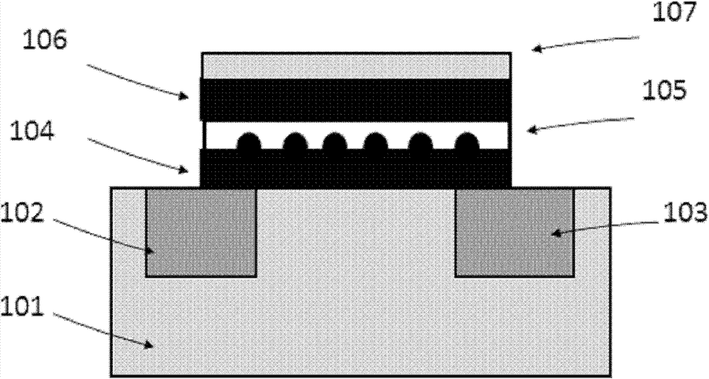
在本发明的一个示例性实施例中,提供了一种金属纳米晶存储器。图1A为本发明实施例金属纳米晶存储器的剖面示意图。图1B为本发明实施例纳米晶存储器的三维结构示意图。如图1A及图1B所示,本实施例金属纳米晶存储器包括:衬底101;形成于衬底沟道区两侧的源端102和漏端103;形成于衬底沟道区上方的隧穿介质层104;形成于隧穿介质层104上方的金属纳米晶存储层105;形成于金属纳米晶存储层105上方的电荷阻挡层106;及形成于电荷阻挡层106上方的栅电极107。其中,该金属纳米晶存储层是由金属纳米晶胶体经喷涂方法沉积于隧穿介质层104上并蒸发金属纳米晶胶体内的溶剂后剩余的金属纳米颗粒形成的。并且,该金属纳米晶胶体是由激光烧蚀的方式产生的。In an exemplary embodiment of the present invention, a metal nanocrystal memory is provided. FIG. 1A is a schematic cross-sectional view of a metal nanocrystal memory according to an embodiment of the present invention. FIG. 1B is a schematic diagram of a three-dimensional structure of a nanocrystalline memory according to an embodiment of the present invention. As shown in FIG. 1A and FIG. 1B , the metal nanocrystalline memory of this embodiment includes: a
本实施例中,金属纳米晶存储层105优选为单层,其颗粒大小介于2~15nm之间(由工艺条件而定),材料为金(Au)、银(Ag)、铂(Pt)等具有较大功函数的金属材料。In this embodiment, the metal
本实施例中,栅电极的材料可以选取贵重金属铂(Pt)、银(Ag)、钯(Pd);CMOS工艺中常用的金属钨(W)、钛(Ti)、铝(Al)、铜(Cu);金属氧化物ITO(氧化铟锡)、IZO(氧化铟锌)等以及多晶硅材料。In this embodiment, the material of the gate electrode can be selected from precious metals platinum (Pt), silver (Ag), palladium (Pd); commonly used metals tungsten (W), titanium (Ti), aluminum (Al), copper (Cu); metal oxides ITO (indium tin oxide), IZO (indium zinc oxide), etc. and polysilicon materials.
本实施例中,隧穿介质层和电荷阻挡层都为高K材料,即具有高介电常数的材料,其介电常数一般高于氮化硅(Si3N4),如氧化铪(HfO2)、氧化铝(Al2O3)或者其它具有类似性质的材料或由多层材料堆叠(如HfO2/Al2O3双层)。In this embodiment, both the tunneling dielectric layer and the charge blocking layer are high-K materials, that is, materials with a high dielectric constant, which are generally higher than silicon nitride (Si 3 N 4 ), such as hafnium oxide (HfO 2 ), aluminum oxide (Al 2 O 3 ) or other materials with similar properties or stacked by multi-layer materials (such as HfO 2 /Al 2 O 3 double-layer).
本实施例中,金属纳米晶存储器综合利用了金属纳米晶的电荷局域化存储特性和高K栅介质的防泄漏特性,能够极大的提升金属纳米晶存储器的存储性能。尤其是,本实施例中,金属纳米晶存储层是由金属纳米晶胶体经喷涂方法沉积于隧穿介质层上的,其纳米颗粒直径可控,均匀性好,无化学污染,可以进一步提升金属纳米晶存储器的性能。In this embodiment, the metal nanocrystal memory comprehensively utilizes the charge localization storage characteristic of the metal nanocrystal and the leakage prevention characteristic of the high-K gate dielectric, which can greatly improve the storage performance of the metal nanocrystal memory. In particular, in this embodiment, the metal nanocrystal storage layer is deposited on the tunneling medium layer by spraying the metal nanocrystal colloid. The diameter of the nanoparticles is controllable, the uniformity is good, and there is no chemical pollution. Performance of Nanocrystalline Memory.
在本发明的另一个示例性实施例中,还提供了一种制备上述金属纳米晶存储器的方法。为了便于说明,首先对衬底上的方向进行规定。In another exemplary embodiment of the present invention, a method for preparing the above-mentioned metal nanocrystal memory is also provided. For the convenience of explanation, the directions on the substrate are specified first.
图2A为由本发明实施例纳米晶存储器构成的NOR型阵列的示意图。如图2A所示,同一行的纳米晶存储器的漏端连接至位线;同一列的纳米晶存储器的栅端连接至字线,其源端连接至源极线(SL)。需要说明的是,图2A所示的NOR型阵列结构和现有技术中的NOR阵列结构相同,此处不再详细描述。FIG. 2A is a schematic diagram of a NOR array composed of nanocrystalline memory according to an embodiment of the present invention. As shown in FIG. 2A , the drains of the nanocrystalline memories in the same row are connected to the bit line; the gates of the nanocrystalline memories in the same column are connected to the word line, and their sources are connected to the source line (SL). It should be noted that the NOR array structure shown in FIG. 2A is the same as the NOR array structure in the prior art, and will not be described in detail here.
图2B为图2A所示NOR型阵列方向的示意图。如图2B所示,A-A’方向对应NOR型阵列的字线方向(WL),B-B’方向对应NOR型阵列的位线方向。以下结合图2B所规定的方向,对本实施例进行详细说明。本发明实施例金属纳米晶存储器制备方法包括:FIG. 2B is a schematic diagram of the orientation of the NOR array shown in FIG. 2A . As shown in FIG. 2B, the A-A' direction corresponds to the word line direction (WL) of the NOR array, and the B-B' direction corresponds to the bit line direction of the NOR array. The present embodiment will be described in detail below in conjunction with the directions specified in FIG. 2B . The method for preparing a metal nanocrystal memory according to the embodiment of the present invention includes:
步骤S302,对衬底进行离子注入及快速退火(用于调整衬底的掺杂浓度分布);沉积牺牲氧化层(用于防止下一步的注入对表面的伤害),并在沉积氧化层之后在所述衬底上进行阈值调整注入和防穿通注入。Step S302, performing ion implantation and rapid annealing on the substrate (for adjusting the doping concentration distribution of the substrate); depositing a sacrificial oxide layer (for preventing damage to the surface by the next implantation), and after depositing the oxide layer Threshold adjustment implantation and punch-through prevention implantation are performed on the substrate.
本步骤中,衬底优选为硅衬底,还可以为锗衬底。离子注入是对衬底表面除浅沟隔离的地方都要进行的步骤,离子注入后,还要进行快速退火,其目的是使得离子均匀掺杂在衬底表面,快速退火的温度大致为500~1000℃不等,与离子注入计量有关。In this step, the substrate is preferably a silicon substrate, and may also be a germanium substrate. Ion implantation is a step that must be carried out on the surface of the substrate except for shallow trench isolation. After ion implantation, rapid annealing is also performed. The purpose is to make ions evenly doped on the substrate surface. The temperature of rapid annealing is roughly 500 ~ It varies from 1000°C, which is related to the ion implantation metering.
步骤S304:在衬底上形成浅沟隔离(Shallow Trench Isolation,简称STI),如图3A及图3B所示;Step S304: forming shallow trench isolation (Shallow Trench Isolation, referred to as STI) on the substrate, as shown in FIG. 3A and FIG. 3B;
其中,图3A为本发明实施例金属纳米晶存储器制备方法中对衬底进行浅沟隔离后沿A-A’方向的结构示意图。图3B为本发明实施例金属纳米晶存储器制备方法中对衬底进行浅沟隔离后沿B-B’方向的结构示意图。在图3A及图3B中,301为浅沟隔离,303和302分别为阈值调整注入和防穿通注入,304为牺牲氧化层。Among them, FIG. 3A is a schematic structural diagram along the A-A' direction after performing shallow trench isolation on the substrate in the method for fabricating the metal nanocrystal memory according to the embodiment of the present invention. Fig. 3B is a schematic diagram of the structure along the B-B' direction after performing shallow trench isolation on the substrate in the method for manufacturing the metal nanocrystal memory according to the embodiment of the present invention. In FIG. 3A and FIG. 3B , 301 is shallow trench isolation, 303 and 302 are threshold adjustment implantation and anti-punching implantation respectively, and 304 is a sacrificial oxide layer.
步骤S306:去掉牺牲氧化层304,淀积高K隧穿介质层104,如图4A及图4B所示;Step S306: removing the
其中,图4A为本发明实施例金属纳米晶存储器制备方法中淀积高K隧穿介质层后沿A-A’方向的结构示意图。图4B为本发明实施例金属纳米晶存储器制备方法中淀积高K隧穿介质层后沿B-B’方向的结构示意图。Among them, FIG. 4A is a schematic diagram of the structure along the A-A' direction after depositing a high-K tunnel dielectric layer in the method for fabricating a metal nanocrystal memory according to an embodiment of the present invention. Fig. 4B is a schematic structural diagram along the B-B' direction after depositing a high-K tunneling dielectric layer in the method for fabricating a metal nanocrystal memory according to an embodiment of the present invention.
本步骤中,隧穿介质层和电荷阻挡层都为高K材料,即具有高介电常数的材料,其介电常数一般高于氮化硅Si3N4,如氧化铪(HfO2)、氧化铝(Al2O3)、氧化钛,氧化锆,铪铝氧,铪氧氮或者其它具有类似性质的材料或由多层材料堆叠(如HfO2/Al2O3双层)具有类似性质的结构。In this step, both the tunneling dielectric layer and the charge blocking layer are high-K materials, that is, materials with a high dielectric constant, whose dielectric constant is generally higher than that of silicon nitride Si 3 N 4 , such as hafnium oxide (HfO 2 ), Aluminum oxide (Al 2 O 3 ), titanium oxide, zirconium oxide, hafnium aluminum oxide, hafnium oxynitride or other materials with similar properties or stacked by multi-layer materials (such as HfO 2 /Al 2 O 3 double layers) have similar properties Structure.
步骤S308,利用喷枪将金属纳米晶胶体喷射沉积在在隧穿介质层上;Step S308, using a spray gun to deposit metal nanocrystal colloids on the tunneling dielectric layer;
本步骤中,金属纳米晶胶体中金属材料为金(Au)、银(Ag)、铂(Pt)等具有较大功函数的金属材料。金属材料的颗粒大小介于2~15nm之间。In this step, the metal material in the metal nanocrystal colloid is gold (Au), silver (Ag), platinum (Pt), and other metal materials with relatively large work functions. The particle size of the metal material is between 2nm and 15nm.
图5A为本发明实施例金属纳米晶存储器制备方法中激光烧蚀法制备金属纳米晶胶体的烧蚀光路图。该烧蚀光路包括:激光器b01,衰减器b02,功率探测器b03,凸透镜b04,全反镜b05;比色皿b06。烧蚀光路中设置激光功率探测器b03和衰减器b02,用于监测和调节激光器的功率。比色皿b06用于放置水溶剂和金属靶材。具体地,金属靶材b07和溶剂b08均放置到比色皿b06中,激光由凸透镜聚焦后再由全反射镜照射在比色皿内的金属靶材中,金属原子或原子团逸出金属靶材表面形成纳米晶颗粒,该金属纳米晶在溶剂b08中形成胶体。5A is an ablation optical path diagram of metal nanocrystal colloid prepared by laser ablation in the method for preparing metal nanocrystal memory according to the embodiment of the present invention. The ablation optical path includes: laser b01, attenuator b02, power detector b03, convex lens b04, total reflection mirror b05; cuvette b06. A laser power detector b03 and an attenuator b02 are set in the ablation optical path for monitoring and adjusting the power of the laser. Cuvette b06 is used to place water solvent and metal target. Specifically, both the metal target b07 and the solvent b08 are placed in the cuvette b06, the laser is focused by the convex lens and then irradiated by the total reflection mirror on the metal target in the cuvette, and the metal atoms or atomic groups escape from the metal target Nanocrystalline particles are formed on the surface, and the metal nanocrystals form a colloid in solvent b08.
此处,本实施例溶剂b08采用水溶剂,在其中加入十二烷基硫酸钠(SDS)或对四-(4-N-甲基吡啶)卟啉(H2TMPyP)作为活性剂。当然,溶剂b08也可以采取有机溶剂,例如乙腈(CH3CN)等,在采用有机溶剂的情况下,就不需要活性剂了。此外,特定的金属可能需要不同的表面活性剂,但以上提的具有较大功函数的金属材料用水溶剂和SDS活性剂即可完全满足要求,并且采用水溶液还具有方便转移、节约成本的优点。采用激光烧蚀制备的纳米晶具有颗粒均匀性好,无化学污染等优点,此外,具体操作过程中,可以通过调整激光器的功率和波长来调节纳米颗粒产生的速率和大小。Here, the solvent b08 of this embodiment is a water solvent, in which sodium dodecyl sulfate (SDS) or p-tetrakis-(4-N-methylpyridine) porphyrin (H2TMPyP) is added as an active agent. Of course, the solvent b08 can also be an organic solvent, such as acetonitrile (CH3CN), etc., and in the case of using an organic solvent, no active agent is needed. In addition, specific metals may require different surfactants, but the above-mentioned metal materials with larger work functions can fully meet the requirements with water solvent and SDS active agent, and the use of aqueous solution has the advantages of convenient transfer and cost saving. Nanocrystals prepared by laser ablation have the advantages of good particle uniformity and no chemical pollution. In addition, during the specific operation process, the rate and size of nanoparticle generation can be adjusted by adjusting the power and wavelength of the laser.
以制备银纳米晶为例,使用Nd:YAG激光器产生的倍频光532nm,脉宽10ns,重复频率10Hz。通过衰减器以调节光强并分出40%用于监测功率。烧蚀光束经150mm石英透镜聚焦在浸没在水溶液中的金属靶上;激光烧蚀出来了的银纳米颗粒,将会融于水溶液中形成银纳米晶胶体。Taking the preparation of silver nanocrystals as an example, the frequency doubled light generated by Nd:YAG laser is 532nm, the pulse width is 10ns, and the repetition frequency is 10Hz. Through the attenuator to adjust the light intensity and split 40% for monitoring power. The ablation beam is focused on the metal target immersed in the aqueous solution through a 150mm quartz lens; the silver nanoparticles ablated by the laser will melt in the aqueous solution to form silver nanocrystal colloids.
在比色皿b06中的金属纳米晶胶体通过胶头滴管或小量杯转移至上述喷枪的样品腔c01中。The metal nanocrystal colloid in the cuvette b06 is transferred to the sample chamber c01 of the above-mentioned spray gun through a glue tip dropper or a small measuring cup.
图5B为本发明实施例金属纳米晶存储器制备方法中沉积金属纳米晶胶体所用喷枪的示意图。本实施例中采用的喷枪为日本扶桑精机株式会社的Richpen 112B型喷枪。沉积金属纳米晶胶体的过程包括:首先将制备的金属纳米晶胶体装入样品腔c01,将已沉积隧穿介质层的衬底放置于加热台c05上;通过氮气入口c02和c03通入氮气(或惰性气体)作为保护气体,以保证整个过程是在保护氛围下完成;喷枪头c04将样品腔c01中的纳米晶胶体喷射在放置于加热台c05上的高温衬底上。对于不同的材料,喷枪设置的参数有所不同,以银纳米晶胶体为例,加热台的温度为190摄氏度,氮气气压为2bar,通过喷枪上的流量按钮调节流量来控制最后的厚度,优选的,纳米晶存储层的厚度为一层纳米晶。FIG. 5B is a schematic diagram of a spray gun used for depositing metal nanocrystal colloid in the method for preparing a metal nanocrystal memory according to an embodiment of the present invention. The spray gun that adopts in the present embodiment is the Richpen 112B type spray gun of Japan Fuso Seiki Co., Ltd. The process of depositing metal nanocrystal colloids comprises: at first the prepared metal nanocrystal colloids are loaded into the sample chamber c01, the substrate of the deposited tunnel dielectric layer is placed on the heating table c05; nitrogen gas is fed through nitrogen gas inlets c02 and c03 ( or inert gas) as a protective gas to ensure that the entire process is completed under a protective atmosphere; the spray gun head c04 sprays the nanocrystalline colloid in the sample chamber c01 on the high-temperature substrate placed on the heating table c05. For different materials, the parameters of spray gun settings are different. Taking silver nanocrystalline colloid as an example, the temperature of the heating table is 190 degrees Celsius, and the nitrogen pressure is 2bar. Adjust the flow rate through the flow button on the spray gun to control the final thickness. , the thickness of the nanocrystal storage layer is one layer of nanocrystal.
步骤S210,使金属纳米晶胶体中的溶剂挥发,剩余金属纳米晶在所述隧穿介质层表面形成金属纳米晶存储层105,如图6A及图6B所示;Step S210, volatilize the solvent in the metal nanocrystal colloid, and the remaining metal nanocrystals form a metal
图6A为本发明实施例金属纳米晶存储器制备方法中形成金属纳米晶存储层后沿A-A’方向的结构示意图。图6B为本发明实施例金属纳米晶存储器制备方法中形成金属纳米晶存储层后沿B-B’方向的结构示意图。Fig. 6A is a schematic structural diagram along the A-A' direction after forming a metal nanocrystal storage layer in the method for fabricating a metal nanocrystal memory according to an embodiment of the present invention. Fig. 6B is a schematic structural diagram along the B-B' direction after forming a metal nanocrystal storage layer in the method for fabricating a metal nanocrystal memory according to an embodiment of the present invention.
本步骤中,可以将金属纳米晶胶体的水分自然晾干,也可以将所述喷涂沉积金属纳米晶胶体的衬底在烘干箱内190度下,氮气氛下,烘干180分钟。采用烘干箱,可以节约时间,而且水分残余少,有利于后期步骤的实现。In this step, the moisture of the metal nanocrystal colloid can be dried naturally, or the substrate on which the metal nanocrystal colloid is sprayed and deposited can be dried for 180 minutes in a drying oven at 190 degrees under a nitrogen atmosphere. The use of a drying box can save time, and there is less water residue, which is conducive to the realization of the later steps.
步骤S212,在金属纳米晶存储层上淀积高K介质的电荷阻挡层106,如图7A及图7B所示;Step S212, depositing a high-K dielectric
图7A为本发明实施例金属纳米晶存储器制备方法中淀积电荷阻挡层后沿A-A’方向的结构示意图。图7B为本发明实施例金属纳米晶存储器制备方法中淀积电荷阻挡层后沿B-B’方向的结构示意图。Fig. 7A is a schematic structural diagram along the direction A-A' after depositing a charge blocking layer in the method for fabricating a metal nanocrystal memory according to an embodiment of the present invention. Fig. 7B is a schematic diagram of the structure along the B-B' direction after depositing the charge blocking layer in the method for fabricating the metal nanocrystal memory according to the embodiment of the present invention.
本步骤中,电荷阻挡层的材料与上述隧穿介质层的材料相似,此处不再详细描述。In this step, the material of the charge blocking layer is similar to that of the aforementioned tunneling dielectric layer, and will not be described in detail here.
步骤S212,沿A-A’方向刻蚀,将浅槽隔离上方的隧穿层、纳米晶存储层和阻挡层刻蚀掉;Step S212, etching along the A-A' direction, etching away the tunneling layer, nanocrystalline storage layer and barrier layer above the shallow trench isolation;
图8为本发明实施例金属纳米晶存储器制备方法中A-A’方向经过刻蚀后的结构示意图。Fig. 8 is a schematic diagram of the structure after etching in the A-A' direction in the method for preparing the metal nanocrystal memory according to the embodiment of the present invention.
步骤S214,在进行刻蚀后的衬底上沉积栅极材料107,如图9A和9B所示;Step S214, depositing a
图9A为本发明实施例金属纳米晶存储器制备方法中沉积栅极后沿A-A’方向的结构示意图。图9B为本发明实施例金属纳米晶存储器制备方法中沉积栅极后沿B-B’方向的结构示意图。Fig. 9A is a schematic diagram of the structure along the direction A-A' after depositing the gate in the method for fabricating the metal nanocrystal memory according to the embodiment of the present invention. Fig. 9B is a schematic diagram of the structure along the B-B' direction after the gate electrode is deposited in the method for fabricating the metal nanocrystal memory according to the embodiment of the present invention.
本步骤中,其中栅极为多晶硅、金属、金属硅化物或由多层材料堆叠具有类似性质的结构。In this step, the gate is polysilicon, metal, metal silicide or a structure with similar properties stacked by multiple layers of materials.
步骤S216,在沉积栅极后的衬底上沿B-B’方向进行刻蚀,刻蚀掉衬底上方的隧穿层、纳米晶存储层、阻挡层和栅极材料层,形成栅极107,如图10所示;Step S216, etching along the BB' direction on the substrate after the gate is deposited, etching away the tunneling layer, nanocrystalline storage layer, barrier layer and gate material layer above the substrate to form the
图10为本发明实施例金属纳米晶存储器制备方法中沿B-B’方向进行刻蚀后沿B-B’方向的结构示意图。Fig. 10 is a schematic diagram of the structure along the B-B' direction after etching along the B-B' direction in the method for preparing a metal nanocrystal memory according to an embodiment of the present invention.
步骤S218,在刻蚀露出的硅衬底上(B-B’方向)入形成源端和漏端,如图11所示;Step S218, forming a source terminal and a drain terminal on the silicon substrate exposed by etching (B-B' direction), as shown in FIG. 11 ;
图11为本发明实施例金属纳米晶存储器制备方法中形成源端和漏端后沿B-B’方向的结构示意图。图11中,102为与沟道区掺杂类型相反的漏极掺杂区,103为与沟道区掺杂类型相反的源极掺杂区,且源极沿A-A’方向为公共相通的,形成共源极(common source)结构,a03为防穿通注入区,a04为侧墙。Fig. 11 is a schematic diagram of the structure along the B-B' direction after the source terminal and the drain terminal are formed in the method for fabricating the metal nanocrystal memory according to the embodiment of the present invention. In Fig. 11, 102 is the drain doping region opposite to the doping type of the channel region, 103 is the source doping region opposite to the doping type of the channel region, and the source is in common communication along the A-A' direction Yes, a common source structure is formed, a03 is the anti-penetration injection region, and a04 is the side wall.
步骤S220,制作金属电极,分别由漏极掺杂区及栅极区引出位线及字线,形成非挥发存储器阵列。其中,电极材料可以为金属,多晶硅,金属性氧化物,硅化物等材料。In step S220 , metal electrodes are fabricated, and bit lines and word lines are respectively drawn out from the doped drain region and the gate region to form a non-volatile memory array. Wherein, the electrode material can be metal, polysilicon, metal oxide, silicide and other materials.
综上所述,本发明纳米晶存储器综合利用了纳米晶的电荷局域化存储特性和高K栅介质的防泄漏特性,可以提供金属纳米晶存储器的综合存储性能。进一步,本发明提供的纳米晶存储器,是基于激光烧蚀、喷枪喷涂的方法来实现,与常规的制备纳米晶浮栅非挥发性存储器比较,具有成本低廉、纳米颗粒直径可控,均匀性好,无污染、器件性能优良等诸多优点。In summary, the nanocrystal memory of the present invention comprehensively utilizes the charge localized storage characteristics of nanocrystals and the leakage prevention characteristics of high-K gate dielectrics, and can provide the comprehensive storage performance of metal nanocrystal memory. Furthermore, the nanocrystalline memory provided by the present invention is realized based on the method of laser ablation and spray gun spraying. Compared with the conventional preparation of nanocrystalline floating gate non-volatile memory, it has low cost, controllable nanoparticle diameter, and good uniformity. , No pollution, excellent device performance and many other advantages.
以上所述的具体实施例,对本发明的目的、技术方案和有益效果进行了进一步详细说明,所应理解的是,以上所述仅为本发明的具体实施例而已,并不用于限制本发明,凡在本发明的精神和原则之内,所做的任何修改、等同替换、改进等,均应包含在本发明的保护范围之内。The specific embodiments described above have further described the purpose, technical solutions and beneficial effects of the present invention in detail. It should be understood that the above descriptions are only specific embodiments of the present invention and are not intended to limit the present invention. Any modifications, equivalent replacements, improvements, etc. made within the spirit and principles of the present invention shall be included within the protection scope of the present invention.
Claims (8)
Priority Applications (1)
| Application Number | Priority Date | Filing Date | Title |
|---|---|---|---|
| CN2011104296082A CN103178062A (en) | 2011-12-20 | 2011-12-20 | Metal nanocrystalline storage |
Applications Claiming Priority (1)
| Application Number | Priority Date | Filing Date | Title |
|---|---|---|---|
| CN2011104296082A CN103178062A (en) | 2011-12-20 | 2011-12-20 | Metal nanocrystalline storage |
Publications (1)
| Publication Number | Publication Date |
|---|---|
| CN103178062A true CN103178062A (en) | 2013-06-26 |
Family
ID=48637819
Family Applications (1)
| Application Number | Title | Priority Date | Filing Date |
|---|---|---|---|
| CN2011104296082A Pending CN103178062A (en) | 2011-12-20 | 2011-12-20 | Metal nanocrystalline storage |
Country Status (1)
| Country | Link |
|---|---|
| CN (1) | CN103178062A (en) |
Citations (5)
| Publication number | Priority date | Publication date | Assignee | Title |
|---|---|---|---|---|
| CN101020999A (en) * | 2007-03-23 | 2007-08-22 | 沈阳航空工业学院 | Planar reciprocating process and apparatus for spraying to deposit multilayer composite material |
| CN200984643Y (en) * | 2006-12-19 | 2007-12-05 | 浙江工业大学 | Device for preparing metal nanometer particle colloid with pulse laser ablation in liquid phase |
| CN101452963A (en) * | 2007-12-05 | 2009-06-10 | 中国科学院微电子研究所 | Metal nanocrystalline floating gate non-volatile memory and manufacturing method thereof |
| CN101512754A (en) * | 2006-07-28 | 2009-08-19 | 奈米系统股份有限公司 | Methods and devices for forming nanostructured monolayers, and devices comprising such monolayers |
| US20100196192A1 (en) * | 2009-01-30 | 2010-08-05 | Imra America, Inc. | Production of metal and metal-alloy nanoparticles with high repetition rate ultrafast pulsed laser ablation in liquids |
-
2011
- 2011-12-20 CN CN2011104296082A patent/CN103178062A/en active Pending
Patent Citations (5)
| Publication number | Priority date | Publication date | Assignee | Title |
|---|---|---|---|---|
| CN101512754A (en) * | 2006-07-28 | 2009-08-19 | 奈米系统股份有限公司 | Methods and devices for forming nanostructured monolayers, and devices comprising such monolayers |
| CN200984643Y (en) * | 2006-12-19 | 2007-12-05 | 浙江工业大学 | Device for preparing metal nanometer particle colloid with pulse laser ablation in liquid phase |
| CN101020999A (en) * | 2007-03-23 | 2007-08-22 | 沈阳航空工业学院 | Planar reciprocating process and apparatus for spraying to deposit multilayer composite material |
| CN101452963A (en) * | 2007-12-05 | 2009-06-10 | 中国科学院微电子研究所 | Metal nanocrystalline floating gate non-volatile memory and manufacturing method thereof |
| US20100196192A1 (en) * | 2009-01-30 | 2010-08-05 | Imra America, Inc. | Production of metal and metal-alloy nanoparticles with high repetition rate ultrafast pulsed laser ablation in liquids |
Similar Documents
| Publication | Publication Date | Title |
|---|---|---|
| CN101252148B (en) | Nonvolatile memory electronic device and its manufacture method | |
| CN110459611B (en) | Ferroelectric field effect transistor and preparation method thereof | |
| CN101692463B (en) | Capacitor structure of mixed nano-crystal memory and preparation method thereof | |
| CN107170828A (en) | A kind of ferro-electric field effect transistor and preparation method thereof | |
| KR20190129223A (en) | Oxide semiconductor thin film photo transistor and method of manufacturing the same | |
| CN101312213A (en) | Non-volatile memory unit with nanocrystalline floating gate structure and manufacturing method thereof | |
| CN101420012A (en) | Non-volatile resistance transition type memory embedded with nanocrystalline particles | |
| CN102468342A (en) | A kind of semiconductor storage unit, device and preparation method thereof | |
| CN104882490B (en) | A kind of preparation method of the floating-gate memory based on metal hetero quntum point | |
| CN100477095C (en) | Sputtering deposition preparation method of high-density ruthenium nanocrystals suitable for flash memory | |
| CN103247629B (en) | A kind of non-volatile memory and preparation method thereof | |
| CN101383379A (en) | Nanocrystalline floating gate memory with multi-medium composite tunneling layer and manufacturing method thereof | |
| CN101399289A (en) | Nanocrystalline floating gate nonvolatile memory with double-layer tunneling medium structure and manufacturing method | |
| CN101330008A (en) | A method of making metal nanocrystal non-volatile memory | |
| Cui et al. | Improvement of the charge retention of a non-volatile memory by a bandgap-engineered charge trap layer | |
| CN101312212A (en) | Nonvolatile memory using high-k dielectric and nanocrystalline floating gate and manufacturing method thereof | |
| CN103178062A (en) | Metal nanocrystalline storage | |
| CN112436010B (en) | Flexible memory based on two-dimensional material | |
| CN103178017A (en) | A kind of preparation method of metal nanocrystal memory | |
| CN114744111B (en) | A threshold transition device and its preparation method | |
| US20100044775A1 (en) | Semiconductor memory device and semiconductor device | |
| CN106887519B (en) | Preparation method of resistive random access memory for realizing multi-value storage | |
| CN103915566B (en) | Memory device based on phase change quantum dots and manufacturing method thereof | |
| CN103413787B (en) | Preparation method of step-shaped oxide layer Au/SiO2/Si nano-column memory device | |
| CN100583400C (en) | Preparation method of non-volatile memory |
Legal Events
| Date | Code | Title | Description |
|---|---|---|---|
| C06 | Publication | ||
| PB01 | Publication | ||
| C10 | Entry into substantive examination | ||
| SE01 | Entry into force of request for substantive examination | ||
| C02 | Deemed withdrawal of patent application after publication (patent law 2001) | ||
| WD01 | Invention patent application deemed withdrawn after publication |
Application publication date: 20130626 |