[go: up one dir, main page]

CN103137809A - Light emitting diode with current diffusion structure and manufacturing method thereof - Google Patents

Light emitting diode with current diffusion structure and manufacturing method thereof Download PDF

Info

Publication number
CN103137809A
CN103137809A CN2011103988917A CN201110398891A CN103137809A CN 103137809 A CN103137809 A CN 103137809A CN 2011103988917 A CN2011103988917 A CN 2011103988917A CN 201110398891 A CN201110398891 A CN 201110398891A CN 103137809 A CN103137809 A CN 103137809A
Authority
CN
China
Prior art keywords
semiconductor layer
type semiconductor
layer
barrier layer
substrate
Prior art date
Legal status (The legal status is an assumption and is not a legal conclusion. Google has not performed a legal analysis and makes no representation as to the accuracy of the status listed.)
Pending
Application number
CN2011103988917A
Other languages
Chinese (zh)
Inventor
陈复邦
颜伟昱
张智松
Current Assignee (The listed assignees may be inaccurate. Google has not performed a legal analysis and makes no representation or warranty as to the accuracy of the list.)
High Power Opto Inc
Original Assignee
High Power Opto Inc
Priority date (The priority date is an assumption and is not a legal conclusion. Google has not performed a legal analysis and makes no representation as to the accuracy of the date listed.)
Filing date
Publication date
Application filed by High Power Opto Inc filed Critical High Power Opto Inc
Priority to CN2011103988917A priority Critical patent/CN103137809A/en
Publication of CN103137809A publication Critical patent/CN103137809A/en
Pending legal-status Critical Current

Links

Images

Landscapes

  • Led Devices (AREA)

Abstract

一种具电流扩散结构的发光二极管与其制造方法,其包含一N型电极、一N型半导体层、一电流阻挡层、一发光层、一P型半导体层与一P型电极,其中该N型半导体层、该发光层与该P型半导体层形成三明治结构,该N型电极与该P型电极分别设置在该N型半导体层与该P型半导体层上,且本发明为让该电流阻挡层对应该N型电极的图案分布埋设在该N型半导体层内,据此本发明通过让该电流阻挡层埋设在该N型半导体层内,除了可让该N型电极所产生的电流绕过该电流阻挡层而均匀地通过该发光层之外,更可避免接口效应造成阻抗增加,因而可以提升发光效率,且本发明可让该发光层的主要发光区远离该N型电极,可减少该N型电极的光遮蔽量而提升发光亮度。

Figure 201110398891

A light emitting diode with a current diffusion structure and a manufacturing method thereof, comprising an N-type electrode, an N-type semiconductor layer, a current blocking layer, a light emitting layer, a P-type semiconductor layer and a P-type electrode, wherein the N-type semiconductor layer, the light emitting layer and the P-type semiconductor layer form a sandwich structure, the N-type electrode and the P-type electrode are respectively arranged on the N-type semiconductor layer and the P-type semiconductor layer, and the present invention allows the current blocking layer to be buried in the N-type semiconductor layer corresponding to the pattern distribution of the N-type electrode. Accordingly, by burying the current blocking layer in the N-type semiconductor layer, the present invention can not only allow the current generated by the N-type electrode to bypass the current blocking layer and pass through the light emitting layer uniformly, but also avoid the increase of impedance caused by the interface effect, thereby improving the light emitting efficiency. In addition, the present invention can allow the main light emitting area of the light emitting layer to be away from the N-type electrode, which can reduce the light shielding amount of the N-type electrode and improve the light emitting brightness.

Figure 201110398891

Description

A kind of light-emitting diode of tool current spread structure and its manufacture method
Technical field
The relevant light-emitting diode of the present invention refers to increase the light-emitting diode of luminous efficiency especially.
Background technology
Mainly formed by the multiple crystalline substance of heap of stone of luminous semi-conducting material in light-emitting diode (Light Emitting Diode, LED), take blue light-emitting diode as example.It mainly is comprised of gallium nitrate based (GaN-based) brilliant film of heap of stone, and storehouse forms the sandwich structure with a n type semiconductor layer, a luminescent layer and a p type semiconductor layer.
see also shown in Figure 1, be a kind of existing level formula light-emitting diode 1, it inserts current barrier layer 3 in P type semiconductor 2, so that scattered current can uniformly luminously increase luminous efficiency by luminescent layer 4 by stopping of current barrier layer 3, yet this kind horizontal light emitting diode structure, the first the sky of its light-emitting zone is restricted, in order to reduce the light masking amount of electrode, its P type electrode 5 adopts transparent conductive layer (as tin indium oxide) mostly, to increase light transmittance, yet the conductance of tin indium oxide is not good, easily cause interface effect, cause impedance to increase, its luminous efficiency can't effectively improve.
See also shown in Figure 2, be the existing vertical LED 6 of another kind, it must not adopt transparency conducting layer, thereby there is no not good problem of tin indium oxide conductance, yet it allows this current barrier layer 7 be arranged between P type semiconductor 8 and P type electrode 9, it causes P type semiconductor 8 and the contact area of P type electrode 9 to reduce, and still can cause the increase of impedance, and can't effectively improve luminous efficiency.
Obviously, prior art is in scattered current, and the demand on using is satisfied in the increase of its uncontrollable impedance, thereby can't really improve luminous efficiency.
Summary of the invention
Main purpose of the present invention is to disclose a kind of light emitting diode construction, and it can effectively control contact impedance, with certain improving luminous efficiency, and the demand on satisfied the use.
Secondary objective of the present invention is to disclose a kind of light emitting diode construction manufacture method, producing the light emitting diode construction that can effectively control contact impedance, and improving luminous efficiency, to satisfy the demand on using.
via as can be known above, for reaching above-mentioned purpose, the present invention is a kind of light-emitting diode of tool current spread structure, it comprises: a n type semiconductor layer, one luminescent layer, one p type semiconductor layer, one N-type electrode, one P type electrode and a current barrier layer, wherein this luminescent layer is arranged on a side of this n type semiconductor layer, this p type semiconductor layer is arranged on this luminescent layer away from a side of this n type semiconductor layer, this N-type electrode has a pattern and distributes, and be arranged on this n type semiconductor layer away from a side of this luminescent layer, this P type electrode is arranged on this p type semiconductor layer away from a side of this luminescent layer, this current barrier layer has that this pattern distributes and to being embedded in this n type semiconductor layer by the N-type electrode.
Preferably, this current barrier layer is made for being selected from metal oxide.
Preferably, this current barrier layer is to be selected from the group that titanium dioxide and silicon dioxide forms to make.
Preferably, the thickness of this current barrier layer is 10~500 nanometers.
Preferably, this n type semiconductor layer comprises one first n type semiconductor layer and one second n type semiconductor layer, and this current barrier layer is arranged between this first n type semiconductor layer and this second n type semiconductor layer.
Preferably, between this P type electrode and this p type semiconductor layer, a metallic reflector is set more, this metallic reflector is to be selected from the group that aluminium, nickel, silver and titanium form to make.
Preferably, between this metallic reflector and this P type electrode, a barrier layer, a binder course and a permanent substrate are set more, this barrier layer is to be selected from the group that titanium, tungsten, platinum, nickel, aluminium and chromium forms to make, this binder course is that any that be selected from gold-tin alloy, golden indium alloy and golden lead alloy made, and this permanent substrate is that any that be selected from silicon substrate, copper base, copper tungsten substrate, aluminium nitride substrate and titanium nitride substrate made.
And manufacture method of the present invention, its step is for first longly on a temporary substrate brilliantly forming this n type semiconductor layer, being embedded in the structures such as this current barrier layer, this luminescent layer and this p type semiconductor layer in this n type semiconductor layer, turn again and bind after on a permanent substrate, remove this temporary substrate, namely complete after plating at last this N-type electrode and this P type electrode.
Accordingly, the present invention is by burying the mode of this current barrier layer in this n type semiconductor layer, in scattered current, can effectively control contact impedance, and the present invention can allow the main luminous zone of this luminescent layer away from this N-type electrode, certain improving luminous efficiency with the light masking amount that reduces this N-type electrode, and the demand on satisfied the use.
Description of drawings
Fig. 1 is existing light emitting diode construction figure;
Fig. 2 is another existing light emitting diode construction figure;
Fig. 3 A is light emitting diode construction figure of the present invention;
Fig. 3 B is LED current flow graph of the present invention;
Fig. 4 A~4E is light-emitting diode manufacturing flow chart of the present invention.
Embodiment
Hereby relevant detailed content of the present invention and technical descriptioon, now be described further with embodiment, but will be appreciated that, these embodiment are the use for illustrating only, and should not be interpreted as restriction of the invention process.
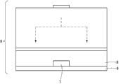
see also shown in Fig. 3 A, the present invention is a kind of light-emitting diode of tool current spread structure, it comprises a n type semiconductor layer 10, one luminescent layer 20, one p type semiconductor layer 30, one N-type electrode 40, one P type electrode 50 and a current barrier layer 60, wherein this luminescent layer 20 is arranged on a side of this n type semiconductor layer 10, this p type semiconductor layer 30 is arranged on this luminescent layer 20 away from a side of this n type semiconductor layer 10, this N-type electrode 40 has a pattern and distributes, and be arranged on this n type semiconductor layer 10 away from a side of this luminescent layer 20, this P type electrode 50 is arranged on this p type semiconductor layer 30 away from a side of this luminescent layer 20.
This luminescent layer 20 can select common gallium nitride or InGaN to make, gallium nitride, aluminium gallium nitride alloy or aluminum indium nitride gallium that n type semiconductor layer 10 can be selected doped silicon etc. made, and 30 of p type semiconductor layers can select magnesium-doped gallium nitride, aluminium gallium nitride alloy or aluminum indium nitride gallium etc. to make.
And this current barrier layer 60 has that this pattern distributes and to being embedded in this n type semiconductor layer 10 by N-type electrode 40, and this n type semiconductor layer 10 can comprise one first n type semiconductor layer 11 and one second n type semiconductor layer 12,60 of this current barrier layers are arranged between this first n type semiconductor layer 11 and this second n type semiconductor layer 12, this current barrier layer 60 is made for being selected from metal oxide again, this current barrier layer 60 can be made for being selected from the group that titanium dioxide and silicon dioxide forms, and the thickness of this current barrier layer 60 can be 10~500 nanometers.The surface 111 of another this first n type semiconductor layer 11 can roughening to increase the contact area with this N-type electrode 40.
In addition, between this P type electrode 50 and this p type semiconductor layer 30, a metallic reflector 70 is set more, this metallic reflector 70 is made for the group that is selected from aluminium, nickel, silver, titanium and forms, and it can be used for the light that this luminescent layer 20 of reflection produces, and increase luminous efficiency, and the effect with conduction.
and between this metallic reflector 70 and this P type electrode 50, a barrier layer 80 is set more, one binder course 81 and a permanent substrate 82, this barrier layer 80 is for being selected from titanium, tungsten, platinum, nickel, aluminium, the group that chromium forms makes, this barrier layer 80 in order to block this binder course 81 in conjunction with the time destruction that this p type semiconductor layer 30 is caused, and in order to conduction, heat radiation, and this binder course 81 is for being selected from gold-tin alloy, the gold indium alloy, any of gold lead alloy made, has conduction, heat radiation waits effect with bonding, this permanent substrate 82 is for being selected from silicon substrate, copper base, the copper tungsten substrate, any of aluminium nitride substrate and titanium nitride substrate made, and in order to conduction, heat radiation, to increase radiating efficiency.
See also shown in Fig. 3 B, the present invention is by allowing this current barrier layer 60 be embedded in this n type semiconductor layer 10, except the electric current 41 that can allow this N-type electrode 40 produce is walked around this current barrier layer 60 and is passed through equably this luminescent layer 20, more can avoid interface effect to cause impedance to increase, thereby can improving luminous efficiency, and the present invention can allow the main luminous zone (being that electric current 41 is intensive by the district) of this luminescent layer 20 away from this N-type electrode 40, promote brightness with the light masking amount that reduces this N-type electrode 40.
Please consult again shown in Fig. 4 A~Fig. 4 E, and the method for manufacturing light-emitting of tool current spread structure of the present invention, its step is as described below.
at first, as shown in Fig. 4 A, long brilliant one first n type semiconductor layer 11 that forms on a temporary substrate 90, it can select the gallium nitride of doped silicon, aluminium gallium nitride alloy or aluminum indium nitride gallium etc. are made, and can be before long brilliant this first n type semiconductor layer 11 of formation on this temporary substrate 90, first form a buffer semiconductor layer 91 on this temporary substrate 90, buffering by this buffer semiconductor layer 91, can reduce the defective of this first n type semiconductor layer 11, this temporary substrate 90 can select the good sapphire substrate of long brilliant characteristic to make, and this buffer semiconductor layer 91 can be selected unadulterated gallium nitride, aluminium gallium nitride alloy or aluminum indium nitride gallium etc. are made.
Then, as shown in Figure 4 B, form the current barrier layer 60 that tool one pattern distributes on this first n type semiconductor layer 11, this current barrier layer 60 can be made for being selected from metal oxide.Can make for being selected from the group that titanium dioxide and silicon dioxide forms as this current barrier layer 60, and the thickness of this current barrier layer 60 can be 10~500 nanometers.
Then, as shown in Fig. 4 C, side direction is long brilliant on this first n type semiconductor layer 11 forms one second n type semiconductor layer 12 and coats and bury this current barrier layer 60, and gallium nitride, aluminium gallium nitride alloy or aluminum indium nitride gallium that this second n type semiconductor layer 12 can be selected doped silicon equally etc. made.
Then, form a luminescent layer 20 on this second n type semiconductor layer 12, this luminescent layer 20 can select gallium nitride or InGaN to make.
Then, form a p type semiconductor layer 30 on this luminescent layer 20,30 of p type semiconductor layers can select magnesium-doped gallium nitride, aluminium gallium nitride alloy or aluminum indium nitride gallium etc. to make.
Then, form a metallic reflector 70 on this p type semiconductor layer 30, this metallic reflector 70 can be made for being selected from the group that aluminium, nickel, silver, titanium forms, its high reflectance by this metallic reflector 70 can reflect the light that this luminescent layer 20 produces, and possesses the effects such as conduction, heat radiation.
Then, form a barrier layer 80 on this metallic reflector 70, this barrier layer 80 is made for the group that is selected from titanium, tungsten, platinum, nickel, aluminium, chromium and forms, and possesses the effects such as conduction, heat radiation.
Then, make this barrier layer 80 by a binder course 81 and permanent substrate 82 combinations, this moment this barrier layer 80 can in order to block this binder course 81 in conjunction with the time destruction that this p type semiconductor layer 30 is caused, and in order to conduction, heat radiation, and this binder course 81 can be made for any that is selected from gold-tin alloy, golden indium alloy, golden lead alloy, and the effect of tool conduction, heat radiation and bonding, this permanent substrate 82 is made for any that is selected from silicon substrate, copper base, copper tungsten substrate, aluminium nitride substrate and titanium nitride substrate, also tool conduction, the effect of dispelling the heat.
Then, as shown in Fig. 4 D, remove this temporary substrate 90 and this buffer semiconductor layer 91, and plate a P type electrode 50 at this permanent substrate 82.
At last, allow surface 111 roughenings of this first n type semiconductor layer 11, and position that should current barrier layer 60 is being plated the N-type electrode 40 that this pattern of tool distributes.
as mentioned above, the present invention is by burying the mode of this current barrier layer 60 in this n type semiconductor layer 10, except the effect that can have these current barrier layer 60 scattered currents, the present invention more can effectively control contact impedance, avoid contact impedance significantly to promote, again by method of the present invention, can form a rectilinear light-emitting diode, P type electrode 50 must not use the transparency conducting layer of high impedance, and the present invention can allow the main luminous zone of this luminescent layer 20 away from this N-type electrode 40, to reduce the light masking amount of this N-type electrode 40, thereby the present invention's improving luminous efficiency really, to satisfy the demand on using.

Claims (14)

1. the light-emitting diode of a tool current spread structure, is characterized in that, comprises:
One n type semiconductor layer;
One luminescent layer, this luminescent layer are arranged on a side of this n type semiconductor layer;
One p type semiconductor layer, this p type semiconductor layer are arranged on this luminescent layer away from a side of this n type semiconductor layer;
One N-type electrode, this N-type electrode have a pattern and distribute, and are arranged on this n type semiconductor layer away from a side of this luminescent layer;
One P type electrode, this P type electrode is arranged on this p type semiconductor layer away from a side of this luminescent layer;
One current barrier layer, this current barrier layer have that this pattern distributes and to being embedded in this n type semiconductor layer by the N-type electrode.
2. the light-emitting diode of tool current spread structure according to claim 1, is characterized in that, this current barrier layer is made for being selected from metal oxide.
3. the light-emitting diode of tool current spread structure according to claim 2, is characterized in that, this current barrier layer is to be selected from the group that titanium dioxide and silicon dioxide forms to make.
4. the light-emitting diode of tool current spread structure according to claim 1, is characterized in that, the thickness of this current barrier layer is 10~500 nanometers.
5. the light-emitting diode of tool current spread structure according to claim 1, it is characterized in that, this n type semiconductor layer comprises one first n type semiconductor layer and one second n type semiconductor layer, and this current barrier layer is arranged between this first n type semiconductor layer and this second n type semiconductor layer.
6. the light-emitting diode of tool current spread structure according to claim 1, is characterized in that, between this P type electrode and this p type semiconductor layer, a metallic reflector is set more, and this metallic reflector is to be selected from the group that aluminium, nickel, silver and titanium form to make.
7. the light-emitting diode of tool current spread structure according to claim 6, it is characterized in that, between this metallic reflector and this P type electrode, a barrier layer, a binder course and a permanent substrate are set more, this barrier layer is to be selected from the group that titanium, tungsten, platinum, nickel, aluminium and chromium forms to make, this binder course is that any that be selected from gold-tin alloy, golden indium alloy and golden lead alloy made, and this permanent substrate is that any that be selected from silicon substrate, copper base, copper tungsten substrate, aluminium nitride substrate and titanium nitride substrate made.
8. the method for manufacturing light-emitting of a tool current spread structure, is characterized in that, step comprises:
Long brilliant one first n type semiconductor layer that forms on a temporary substrate;
Form the current barrier layer that tool one pattern distributes on this first n type semiconductor layer;
Side direction is long brilliant on this first n type semiconductor layer forms one second n type semiconductor layer and coats and bury this current barrier layer;
Form a luminescent layer on this second n type semiconductor layer;
Form a p type semiconductor layer on this luminescent layer;
Form a metallic reflector on this p type semiconductor layer;
Form a barrier layer on this metallic reflector;
This barrier layer is combined with a permanent substrate by a binder course;
Remove this temporary substrate, plate a P type electrode at this permanent substrate;
Allow the surface roughening of this first n type semiconductor layer, and position that should current barrier layer is being plated the N-type electrode that this pattern of tool distributes.
9. the method for manufacturing light-emitting of tool current spread structure according to claim 8, is characterized in that, this current barrier layer is made for being selected from metal oxide.
10. the method for manufacturing light-emitting of tool current spread structure according to claim 9, is characterized in that, this current barrier layer is to be selected from the group that titanium dioxide and silicon dioxide forms to make.
11. the method for manufacturing light-emitting of tool current spread structure according to claim 8 is characterized in that, the thickness of this current barrier layer is 10~500 nanometers.
12. the method for manufacturing light-emitting of tool current spread structure according to claim 8 is characterized in that, this metallic reflector is to be selected from the group that aluminium, nickel, silver and titanium form to make.
13. the method for manufacturing light-emitting of tool current spread structure according to claim 8, it is characterized in that, this barrier layer is to be selected from the group that titanium, tungsten, platinum, nickel, aluminium and chromium forms to make, this binder course is that any that be selected from gold-tin alloy, golden indium alloy and golden lead alloy made, and this permanent substrate is that any that be selected from silicon substrate, copper base, copper tungsten substrate, aluminium nitride substrate and titanium nitride substrate made.
14. the method for manufacturing light-emitting of tool current spread structure according to claim 8, it is characterized in that, before long brilliant this first n type semiconductor layer of formation on this temporary substrate, first form a buffer semiconductor layer on this temporary substrate, and when removing this temporary substrate, remove simultaneously this buffer semiconductor layer.
CN2011103988917A 2011-12-05 2011-12-05 Light emitting diode with current diffusion structure and manufacturing method thereof Pending CN103137809A (en)

Priority Applications (1)

Application Number Priority Date Filing Date Title
CN2011103988917A CN103137809A (en) 2011-12-05 2011-12-05 Light emitting diode with current diffusion structure and manufacturing method thereof

Applications Claiming Priority (1)

Application Number Priority Date Filing Date Title
CN2011103988917A CN103137809A (en) 2011-12-05 2011-12-05 Light emitting diode with current diffusion structure and manufacturing method thereof

Publications (1)

Publication Number Publication Date
CN103137809A true CN103137809A (en) 2013-06-05

Family

ID=48497372

Family Applications (1)

Application Number Title Priority Date Filing Date
CN2011103988917A Pending CN103137809A (en) 2011-12-05 2011-12-05 Light emitting diode with current diffusion structure and manufacturing method thereof

Country Status (1)

Country Link
CN (1) CN103137809A (en)

Cited By (1)

* Cited by examiner, † Cited by third party
Publication number Priority date Publication date Assignee Title
CN106025027A (en) * 2016-07-15 2016-10-12 厦门乾照光电股份有限公司 LED chip structure and manufacturing method thereof

Citations (4)

* Cited by examiner, † Cited by third party
Publication number Priority date Publication date Assignee Title
CN1619850A (en) * 2003-11-21 2005-05-25 三垦电气株式会社 Light-emitting semiconductor device and method of fabrication
CN101107720A (en) * 2005-01-24 2008-01-16 美商克立股份有限公司 Light-emitting diodes using current confinement structures and surface roughening
US20080157115A1 (en) * 2005-06-21 2008-07-03 Epistar Corporation High-efficiency light-emitting device and manufacturing method thereof
US20100320478A1 (en) * 2009-06-19 2010-12-23 Ubilux Optoelectronics Corporation Light-emitting diode device including a current blocking region and method of making the same

Patent Citations (4)

* Cited by examiner, † Cited by third party
Publication number Priority date Publication date Assignee Title
CN1619850A (en) * 2003-11-21 2005-05-25 三垦电气株式会社 Light-emitting semiconductor device and method of fabrication
CN101107720A (en) * 2005-01-24 2008-01-16 美商克立股份有限公司 Light-emitting diodes using current confinement structures and surface roughening
US20080157115A1 (en) * 2005-06-21 2008-07-03 Epistar Corporation High-efficiency light-emitting device and manufacturing method thereof
US20100320478A1 (en) * 2009-06-19 2010-12-23 Ubilux Optoelectronics Corporation Light-emitting diode device including a current blocking region and method of making the same

Cited By (2)

* Cited by examiner, † Cited by third party
Publication number Priority date Publication date Assignee Title
CN106025027A (en) * 2016-07-15 2016-10-12 厦门乾照光电股份有限公司 LED chip structure and manufacturing method thereof
CN106025027B (en) * 2016-07-15 2018-07-13 厦门乾照光电股份有限公司 A kind of LED chip structure and its manufacturing method

Similar Documents

Publication Publication Date Title
CN101248537B (en) Light-emitting diodes with roughened high-index surface layers for high light extraction
CN102194929B (en) Light emitting device
CN102270633B (en) High-power flip-chip array LED chip and manufacturing method thereof
TWI324401B (en) Fabrication method of high-brightness light emitting diode having reflective layer
CN102194947A (en) Light emitting diode and light emitting diode package
CN102867897A (en) Light emitting device
TW201214771A (en) Light emitting device, light emitting device package, and lighting device
CN108140699A (en) Light-emitting component, light-emitting element package and lighting device
CN105355743B (en) Light emitting diode and preparation method thereof
CN106848006A (en) Flip LED chips and preparation method thereof
CN103489981A (en) Light emitting diode and method for manufacturing the same
CN102522400A (en) Anti-electrostatic-damage vertical light-emitting device and manufacturing method thereof
US20130328077A1 (en) Light-emitting element
CN103682011A (en) Semiconductor light emitting element and manufacturing method thereof
CN102194959A (en) Light emitting device, method of manufacturing the light emitting device, light emitting device package, and lighting unit
CN209626251U (en) A kind of semiconductor light-emitting elements, packaging body and light emitting device
TW201644069A (en) Light-emitting element
CN214313229U (en) Flip LED chip
CN106848005A (en) Lift flip LED chips of brightness and preparation method thereof
US20130161669A1 (en) Light-emitting diode with current diffusion structure and a method for fabricating the same
CN103137809A (en) Light emitting diode with current diffusion structure and manufacturing method thereof
CN103594594B (en) There is the inverted light-emitting diode (LED) of roughening transparency electrode
CN103594569B (en) There is the manufacture method of the inverted light-emitting diode (LED) of alligatoring transparency electrode
CN103594591B (en) There is the manufacture method of the inverted light-emitting diode (LED) of transparency electrode
CN102903817B (en) Light emitting device with reflecting electrode

Legal Events

Date Code Title Description
C06 Publication
PB01 Publication
C10 Entry into substantive examination
SE01 Entry into force of request for substantive examination
C02 Deemed withdrawal of patent application after publication (patent law 2001)
WD01 Invention patent application deemed withdrawn after publication

Application publication date: 20130605