CN102738002A - Manufacturing method of semiconductor device - Google Patents
Manufacturing method of semiconductor device Download PDFInfo
- Publication number
- CN102738002A CN102738002A CN2012100987508A CN201210098750A CN102738002A CN 102738002 A CN102738002 A CN 102738002A CN 2012100987508 A CN2012100987508 A CN 2012100987508A CN 201210098750 A CN201210098750 A CN 201210098750A CN 102738002 A CN102738002 A CN 102738002A
- Authority
- CN
- China
- Prior art keywords
- oxide semiconductor
- electrode layer
- film
- insulating film
- semiconductor layer
- Prior art date
- Legal status (The legal status is an assumption and is not a legal conclusion. Google has not performed a legal analysis and makes no representation as to the accuracy of the status listed.)
- Granted
Links
Images


Classifications
-
- H—ELECTRICITY
- H10—SEMICONDUCTOR DEVICES; ELECTRIC SOLID-STATE DEVICES NOT OTHERWISE PROVIDED FOR
- H10D—INORGANIC ELECTRIC SEMICONDUCTOR DEVICES
- H10D30/00—Field-effect transistors [FET]
- H10D30/01—Manufacture or treatment
- H10D30/021—Manufacture or treatment of FETs having insulated gates [IGFET]
- H10D30/031—Manufacture or treatment of FETs having insulated gates [IGFET] of thin-film transistors [TFT]
-
- H—ELECTRICITY
- H10—SEMICONDUCTOR DEVICES; ELECTRIC SOLID-STATE DEVICES NOT OTHERWISE PROVIDED FOR
- H10D—INORGANIC ELECTRIC SEMICONDUCTOR DEVICES
- H10D30/00—Field-effect transistors [FET]
- H10D30/01—Manufacture or treatment
-
- H—ELECTRICITY
- H10—SEMICONDUCTOR DEVICES; ELECTRIC SOLID-STATE DEVICES NOT OTHERWISE PROVIDED FOR
- H10D—INORGANIC ELECTRIC SEMICONDUCTOR DEVICES
- H10D30/00—Field-effect transistors [FET]
- H10D30/60—Insulated-gate field-effect transistors [IGFET]
- H10D30/67—Thin-film transistors [TFT]
- H10D30/6704—Thin-film transistors [TFT] having supplementary regions or layers in the thin films or in the insulated bulk substrates for controlling properties of the device
-
- H—ELECTRICITY
- H10—SEMICONDUCTOR DEVICES; ELECTRIC SOLID-STATE DEVICES NOT OTHERWISE PROVIDED FOR
- H10D—INORGANIC ELECTRIC SEMICONDUCTOR DEVICES
- H10D30/00—Field-effect transistors [FET]
- H10D30/60—Insulated-gate field-effect transistors [IGFET]
- H10D30/67—Thin-film transistors [TFT]
- H10D30/674—Thin-film transistors [TFT] characterised by the active materials
- H10D30/6755—Oxide semiconductors, e.g. zinc oxide, copper aluminium oxide or cadmium stannate
-
- H10P95/90—
Landscapes
- Thin Film Transistor (AREA)
- Engineering & Computer Science (AREA)
- Liquid Crystal (AREA)
- Physics & Mathematics (AREA)
- Condensed Matter Physics & Semiconductors (AREA)
- General Physics & Mathematics (AREA)
- Manufacturing & Machinery (AREA)
- Computer Hardware Design (AREA)
- Microelectronics & Electronic Packaging (AREA)
- Power Engineering (AREA)
- Non-Volatile Memory (AREA)
- Electroluminescent Light Sources (AREA)
- Semiconductor Memories (AREA)
- Metal-Oxide And Bipolar Metal-Oxide Semiconductor Integrated Circuits (AREA)
Abstract
Description
技术领域 technical field
本发明涉及一种半导体装置及半导体装置的制造方法。The present invention relates to a semiconductor device and a method for manufacturing the semiconductor device.
另外,在本说明书中半导体装置是指能够通过利用半导体特性而工作的所有装置,因此电光装置、半导体电路以及电子设备都是半导体装置。In addition, in this specification, a semiconductor device refers to all devices that can operate by utilizing semiconductor characteristics, and therefore electro-optical devices, semiconductor circuits, and electronic equipment are all semiconductor devices.
背景技术 Background technique
近年,使用形成在具有绝缘表面的衬底上的半导体薄膜构成晶体管的技术备受关注。该晶体管被广泛地应用于集成电路(IC)及图像显示装置(显示装置)等电子设备。作为可以用于晶体管的半导体薄膜,硅类半导体材料广为周知,除此之外,作为其他材料,氧化物半导体受到关注。In recent years, a technique of forming a transistor using a semiconductor thin film formed on a substrate having an insulating surface has attracted attention. This transistor is widely used in electronic devices such as integrated circuits (ICs) and image display devices (display devices). Silicon-based semiconductor materials are widely known as semiconductor thin films that can be used in transistors, and oxide semiconductors are attracting attention as other materials.
例如,已经公开有一种作为活性层使用电子载流子浓度低于1018/cm3的包含铟(In)、镓(Ga)及锌(Zn)的非晶氧化物的晶体管(参照专利文献1)。For example, a transistor using an amorphous oxide containing indium (In), gallium (Ga), and zinc (Zn) with an electron carrier concentration of less than 10 18 /cm 3 as an active layer has been disclosed (see Patent Document 1 ).
[专利文献1]日本专利申请公开2006-165528号公报[Patent Document 1] Japanese Patent Application Publication No. 2006-165528
但是,氧化物半导体在装置制造工序中有可能由于形成电子给体的氢或水的混入等或氧从氧化物半导体脱离导致导电率变化。该现象是导致使用氧化物半导体的晶体管的电特性变动的主要原因。However, the conductivity of the oxide semiconductor may change due to the incorporation of hydrogen or water forming an electron donor or detachment of oxygen from the oxide semiconductor during the device manufacturing process. This phenomenon is a main cause of variation in electrical characteristics of transistors using oxide semiconductors.
尤其是,由于具有该晶体管的半导体装置或电子设备的制造工序中的热处理,存在来自大气的水或氢侵入且扩散到氧化物半导体层中而使已形成的晶体管的电特性发生变动。In particular, due to heat treatment in the manufacturing process of a semiconductor device or electronic equipment including the transistor, water or hydrogen from the atmosphere intrudes and diffuses into the oxide semiconductor layer to change the electrical characteristics of the formed transistor.
发明内容 Contents of the invention
鉴于上述问题,本发明的一个方式的目的之一是对使用氧化物半导体的半导体装置赋予稳定的电特性而使其具有高可靠性。In view of the above problems, an object of one embodiment of the present invention is to impart stable electrical characteristics to a semiconductor device using an oxide semiconductor so as to have high reliability.
在包括氧化物半导体层的晶体管的制造工序中,在氧化物半导体层上以与其接触的方式形成栅极绝缘膜,在栅极绝缘膜上形成栅电极层,并且在栅极绝缘膜及栅电极层上以与其接触的方式形成氧化铝膜,由此可以防止由于具有该晶体管的半导体装置或电子设备的制造工序中的热处理来自大气的水或氢侵入且扩散到氧化物半导体层中。In the manufacturing process of a transistor including an oxide semiconductor layer, a gate insulating film is formed on the oxide semiconductor layer so as to be in contact therewith, a gate electrode layer is formed on the gate insulating film, and the gate insulating film and the gate electrode Forming an aluminum oxide film on the layer in contact with it can prevent water or hydrogen from the atmosphere from entering and diffusing into the oxide semiconductor layer due to heat treatment in the manufacturing process of a semiconductor device or electronic device having the transistor.
所公开的发明的一个方式是一种半导体装置的制造方法,包括如下步骤:形成基底绝缘膜;在所述基底绝缘膜上以与其接触的方式形成氧化物半导体层;在所述氧化物半导体层上形成源电极层及漏电极层;在所述氧化物半导体层、源电极层及漏电极层上以与其接触的方式形成栅极绝缘膜;在所述栅极绝缘膜上的与所述氧化物半导体层重叠的区域上形成栅电极层;在所述栅极绝缘膜及所述栅电极层上以与其接触的方式形成氧化铝膜而制造晶体管;对所述晶体管进行热处理;以及将所述氧化铝膜的厚度设定为大于50nm且为500nm以下。One aspect of the disclosed invention is a method of manufacturing a semiconductor device, including the steps of: forming a base insulating film; forming an oxide semiconductor layer on the base insulating film so as to be in contact with it; forming a source electrode layer and a drain electrode layer; forming a gate insulating film on the oxide semiconductor layer, source electrode layer and drain electrode layer in contact with them; forming a gate electrode layer on the region where the material semiconductor layer overlaps; forming a transistor by forming an aluminum oxide film in contact with the gate insulating film and the gate electrode layer; performing heat treatment on the transistor; and The thickness of the aluminum oxide film is set to be greater than 50 nm and not more than 500 nm.
所公开的发明的一个方式是一种半导体装置的制造方法,包括如下步骤:形成基底绝缘膜;在所述基底绝缘膜上以与其接触的方式形成氧化物半导体层;在所述氧化物半导体层上形成源电极层及漏电极层;在所述氧化物半导体层、源电极层及漏电极层上以与其接触的方式形成栅极绝缘膜;在所述栅极绝缘膜上的与所述氧化物半导体层重叠的区域上形成栅电极层;在所述栅极绝缘膜及所述栅电极层上以与其接触的方式形成氧化铝膜;对所述氧化物半导体层进行热处理;以及将所述氧化铝膜的厚度设定为大于50nm且为500nm以下。One aspect of the disclosed invention is a method of manufacturing a semiconductor device, including the steps of: forming a base insulating film; forming an oxide semiconductor layer on the base insulating film so as to be in contact with it; forming a source electrode layer and a drain electrode layer; forming a gate insulating film on the oxide semiconductor layer, source electrode layer and drain electrode layer in contact with them; Forming a gate electrode layer on the region where the semiconductor layer overlaps; forming an aluminum oxide film on the gate insulating film and the gate electrode layer in contact with it; heat-treating the oxide semiconductor layer; and The thickness of the aluminum oxide film is set to be greater than 50 nm and not more than 500 nm.
另外,在上述半导体装置的制造方法中,优选在形成氧化物半导体层之后对氧化物半导体层进一步进行热处理。In addition, in the above method of manufacturing a semiconductor device, it is preferable to further heat-treat the oxide semiconductor layer after forming the oxide semiconductor layer.
另外,在上述半导体装置的制造方法中,还可以在氧化铝膜上形成层间绝缘膜。In addition, in the above method of manufacturing a semiconductor device, an interlayer insulating film may be formed on the aluminum oxide film.
另外,在上述半导体装置的制造方法中,优选层间绝缘膜为氧氮化硅。In addition, in the above method of manufacturing a semiconductor device, it is preferable that the interlayer insulating film is silicon oxynitride.
另外,在上述半导体装置的制造方法中,还可以在形成栅电极层之后,利用离子掺杂法或离子注入法对氧化物半导体层添加杂质元素。In addition, in the above method of manufacturing a semiconductor device, after forming the gate electrode layer, an impurity element may be added to the oxide semiconductor layer by ion doping or ion implantation.
另外,在上述半导体装置的制造方法中.优选边加热边形成氧化物半导体层。In addition, in the above method of manufacturing a semiconductor device, it is preferable to form the oxide semiconductor layer while heating.
另外,在上述半导体装置的制造方法中,优选基底绝缘膜及栅极绝缘膜中的至少一个包括与化学计量比相比氧含量过剩的区域。In addition, in the above method of manufacturing a semiconductor device, it is preferable that at least one of the base insulating film and the gate insulating film includes a region in which the oxygen content is excessive compared to the stoichiometric ratio.
另外,在上述半导体装置的制造方法中,优选根据氧化物半导体层上相邻的源电极层与漏电极层之间的间隔宽度形成的沟道长度为2μm以下。In addition, in the above method of manufacturing a semiconductor device, it is preferable that the length of the channel formed by the interval width between the adjacent source electrode layer and drain electrode layer on the oxide semiconductor layer is 2 μm or less.
在晶体管的制造工序中,通过在依次形成氧化物半导体层、源电极层、漏电极层、栅极绝缘膜、栅电极层之后,在栅极绝缘膜及栅电极层上以与其接触的方式形成厚度大于50nm且在500nm以下的氧化铝膜,可以防止由于具有该晶体管的半导体装置或电子设备的制造工序中的热处理来自大气的水或氢侵入且扩散到氧化物半导体层中。另外,同时还可以防止氧从氧化物半导体层脱离。由此,使用氧化物半导体的半导体装置具有稳定的电特性而能够实现高可靠性。In the manufacturing process of transistors, after sequentially forming an oxide semiconductor layer, a source electrode layer, a drain electrode layer, a gate insulating film, and a gate electrode layer, the gate insulating film and the gate electrode layer are formed to be in contact with them. The aluminum oxide film having a thickness of more than 50 nm and less than 500 nm can prevent intrusion and diffusion of water or hydrogen from the atmosphere into the oxide semiconductor layer due to heat treatment in the manufacturing process of semiconductor devices or electronic equipment having the transistor. In addition, at the same time, detachment of oxygen from the oxide semiconductor layer can be prevented. Accordingly, a semiconductor device using an oxide semiconductor has stable electrical characteristics and can achieve high reliability.
附图说明 Description of drawings
图1A和1B是说明半导体装置的一个方式的平面图及截面图;1A and 1B are a plan view and a cross-sectional view illustrating one mode of a semiconductor device;
图2A至2C是说明说明半导体装置的一个方式的制造方法的截面图;2A to 2C are cross-sectional views illustrating a method of manufacturing a semiconductor device;
图3A至3C是说明说明半导体装置的一个方式的制造方法的截面图;3A to 3C are cross-sectional views illustrating a method of manufacturing a semiconductor device;
图4A至4C是说明半导体装置的一个方式的图;4A to 4C are diagrams illustrating one mode of a semiconductor device;
图5是说明半导体装置的一个方式的图;FIG. 5 is a diagram illustrating an embodiment of a semiconductor device;
图6是说明半导体装置的一个方式的图;FIG. 6 is a diagram illustrating one embodiment of a semiconductor device;
图7是说明半导体装置的一个方式的图;FIG. 7 is a diagram illustrating an embodiment of a semiconductor device;
图8A和8B是说明半导体装置的一个方式的图;8A and 8B are diagrams illustrating one mode of a semiconductor device;
图9A至9C是说明半导体装置的一个方式的图;9A to 9C are diagrams illustrating one mode of a semiconductor device;
图10A至10F是示出电子设备的图;10A to 10F are diagrams illustrating electronic devices;
图11A1、11A2、11B1、11B2是示出比较例样品A的SIMS数据的图;11A1, 11A2, 11B1, 11B2 are graphs showing SIMS data of Comparative Example Sample A;
图12A1、12A2、12B1、12B2是示出实施例样品A的SIMS数据的图;12A1, 12A2, 12B1, 12B2 are graphs showing SIMS data for Example Sample A;
图13A至图13D是示出比较例样品A的TDS数据的图;13A to 13D are graphs showing TDS data of Comparative Example Sample A;
图14A至图14D是示出实施例样品B的TDS数据的图;14A to 14D are graphs showing TDS data of Example Sample B;
图15是示出使用比较例样品C的晶体管的特性的图;15 is a graph showing characteristics of a transistor using Comparative Example Sample C;
图16是示出使用实施例样品C的晶体管的特性的图。FIG. 16 is a graph showing characteristics of a transistor using Sample C of the example.
本发明的选择图为图3A至3C。A selection diagram of the present invention is shown in Figures 3A to 3C.
具体实施方式 Detailed ways
下面,使用附图详细地说明本发明的实施方式。但是,本发明不局限于以下说明,所属技术领域的普通技术人员可以很容易地理解一个事实,就是本发明在不脱离其宗旨及其范围的条件下,其方式及详细内容可以被变换为各种各样的形式。因此,本发明不应该被解释为仅限定于以下所示的实施方式的记载内容中。注意,当利用附图说明发明结构时,在不同的附图中共同使用表示相同对象的符号。此外,当表示相同的部分时,有时利用相同的阴影线,而不特别附加附图标记。另外,为了方便起见,有时不在俯视图中表示绝缘膜。Hereinafter, embodiments of the present invention will be described in detail using the drawings. However, the present invention is not limited to the following descriptions, and those skilled in the art can easily understand the fact that, without departing from the purpose and scope of the present invention, its methods and details can be changed into various in various forms. Therefore, the present invention should not be interpreted as being limited only to the description of the embodiments shown below. Note that when describing the configuration of the invention using drawings, symbols representing the same objects are commonly used in different drawings. In addition, when the same part is shown, the same hatching may be used, and reference numerals are not especially attached. In addition, for the sake of convenience, the insulating film may not be shown in plan view.
注意,在以下说明中,第一、第二等序数词是为了便于说明而使用的,其并不代表对数量的限定。Note that in the following description, ordinal numerals such as first and second are used for convenience of description, and do not represent a limitation on quantity.
实施方式1Embodiment 1
在本实施方式中,参照图1A至图3C对本发明的一个方式的具有晶体管的半导体装置的制造方法进行说明。In this embodiment mode, a method of manufacturing a semiconductor device having a transistor according to one embodiment of the present invention will be described with reference to FIGS. 1A to 3C .
图1A和1B示出顶栅顶接触型的晶体管150的平面图及截面图。图1A是平面图,图1B是沿着图1A中的线A-B的截面图。另外,在图1A中,为了简化起见,省略晶体管150的构成要素的一部分(例如,绝缘膜114等)。1A and 1B show a plan view and a cross-sectional view of a
<本实施方式中的半导体装置的结构><Structure of Semiconductor Device in This Embodiment>
图1A和1B是使用本实施方式的方法制造的半导体装置的结构例。图1A和1B所示的晶体管150包括:衬底100;形成在衬底100上的基底绝缘膜102;基底绝缘膜102上的以与其接触的方式形成的氧化物半导体层106;形成在氧化物半导体层106上的源电极层108a及漏电极层108b;氧化物半导体层106、源电极层108a及漏电极层108b上的以与其接触的方式形成的栅极绝缘膜110;形成在栅极绝缘膜110上的重叠于氧化物半导体层106的区域上的栅电极层112;栅极绝缘膜110及栅电极层112上的以与其接触的方式形成的绝缘膜114;形成在绝缘膜114上的层间绝缘膜116。另外,在形成栅电极层112之后,对氧化物半导体层106添加杂质元素,而在与源电极层108a、漏电极层108b及栅电极层112重叠的区域中形成第一区域106a,在不与源电极层108a、漏电极层108b及栅电极层112重叠的区域中形成第二区域106b、第二区域106c。1A and 1B are structural examples of a semiconductor device manufactured using the method of this embodiment. The
<本实施方式中的半导体装置的制造方法><Method of Manufacturing Semiconductor Device in This Embodiment>
使用图2A至2C和图3A至3C说明晶体管150的制造方法。A method of manufacturing the
首先,在衬底100上形成基底绝缘膜102,在基底绝缘膜102上以与其接触的方式选择性地形成氧化物半导体层106(参照图2A)。First, a
作为衬底100,使用具有绝缘表面的衬底即可。例如,可以使用玻璃衬底、石英衬底、表面上形成有绝缘膜的半导体衬底或表面上形成有绝缘膜的不锈钢衬底等。As the
作为基底绝缘膜102,可以利用溅射法使用氧化硅、氮化硅、氧氮化硅或氮氧化硅等形成。另外,基底绝缘膜102也可以以含有氧化铝、氧化钽、氧化铪、氧化钇、硅酸铪(HfSixOy(x>0、y>0))、添加有氮的硅酸铪(HfSixOy(x>0、y>0))、添加有氮的铝酸铪(HfAlxOy(x>0、y>0))等的方式形成。优选尽量地去除与氧化物半导体层106接触的基底绝缘膜102中的水及氢。另外,基底绝缘膜102既可以为单层也可以为多个层的叠层。The base
注意,在本说明书中,氧氮化硅等的“氧氮化物”是指在其组成中氧含量大于氮含量的物质。Note that in this specification, "oxynitride" of silicon oxynitride or the like refers to a substance whose composition contains more oxygen than nitrogen.
另外,在本说明书中,氮氧化硅等的“氮氧化物”是指在其组成中氮含量大于氧含量的物质。In addition, in this specification, "oxynitride" such as silicon oxynitride refers to a substance whose composition contains more nitrogen than oxygen.
在图1A和1B所示的晶体管150中,优选基底绝缘膜102或栅极绝缘膜110中的至少一方包括与化学计量比相比氧含量过剩的区域。此时,将氧含量设定为大于基底绝缘膜或栅极绝缘膜的化学计量比。例如,当采用其组成由SiOx(x>0)表示的氧化硅膜时,因为氧化硅的化学计量比是Si∶O=1∶2,所以优选使用具有x超过2的氧过剩区域的氧化硅膜。该氧过剩区域存在于氧化硅膜的一部分(包含界面)即可。In
当与氧化物半导体层106接触的绝缘膜具有与化学计量比相比氧含量过剩的区域时,可以防止氧从氧化物半导体层106移动到与其接触的绝缘膜中,并且可以由与氧化物半导体层106接触的绝缘膜对氧化物半导体层106供应氧。When the insulating film in contact with the
作为形成氧化物半导体层106的氧化物半导体使用本征(i型)化或实质上本征(i型)化的氧化物半导体,该氧化物半导体是通过去除了杂质并尽量不包含氧化物半导体的主要成分以外的载流子给体的杂质的方式而被高纯度化的氧化物半导体。As the oxide semiconductor forming the
氧化物半导体层106为单晶、多晶(也称为多晶体)或非晶等的状态。The
作为用作氧化物半导体层106的层,例如可以使用利用溅射法等形成的至少含有选自In、Ga、Sn及Zn中的一种以上的元素的氧化物半导体。例如,可以使用:四元金属氧化物的In-Sn-Ga-Zn-O类氧化物半导体;三元金属氧化物的In-Ga-Zn-O类氧化物半导体、In-Sn-Zn-O类氧化物半导体、In-Al-Zn-O类氧化物半导体、Sn-Ga-Zn-O类氧化物半导体、Al-Ga-Zn-O类氧化物半导体、Sn-Al-Zn-O类氧化物半导体;二元金属氧化物的In-Zn-O类氧化物半导体、Sn-Zn-O类氧化物半导体、Al-Zn-O类氧化物半导体、Zn-Mg-O类氧化物半导体、Sn-Mg-O类氧化物半导体、In-Mg-O类氧化物半导体、In-Ga-O类氧化物半导体;单元金属氧化物的In-O类氧化物半导体、Sn-O类氧化物半导体、Zn-O类氧化物半导体等。此外,也可以在上述氧化物半导体中含有In、Ga、Sn、Zn以外的元素,例如SiO2。As the layer used as the
例如,In-Ga-Zn-O类氧化物半导体是指含有铟(In)、镓(Ga)、锌(Zn)的氧化物半导体,并且对其组成比没有限制。For example, an In-Ga-Zn-O-based oxide semiconductor refers to an oxide semiconductor containing indium (In), gallium (Ga), and zinc (Zn), and its composition ratio is not limited.
另外,作为氧化物半导体层106,可以使用由化学式InMO3(ZnO)m(m>0)表示的薄膜。在此,M表示选自Zn、Ga、Al、Mn及Co中的一种或多种金属元素。例如,作为M,有Ga、Ga及Al、Ga及Mn或Ga及Co等。In addition, as the
当作为氧化物半导体采用In-Ga-Zn-O类材料时,作为所使用的靶材,例如可以使用组成比为In2O3∶Ga2O3∶ZnO=1∶1∶1[摩尔比]的氧化物半导体成膜用靶材。另外,不局限于该靶材的材料及组成,例如也可以使用In2O3∶Ga2O3∶ZnO=1∶1∶2[摩尔比]的氧化物半导体成膜用靶材。When an In-Ga-Zn-O-based material is used as the oxide semiconductor, as the target material used, for example, a composition ratio of In 2 O 3 : Ga 2 O 3 : ZnO=1:1:1 [molar ratio ] target for oxide semiconductor film formation. In addition, the material and composition of the target are not limited, and for example, an oxide semiconductor film-forming target of In 2 O 3 :Ga 2 O 3 : ZnO=1:1:2 [molar ratio] may be used.
另外,当作为氧化物半导体使用In-Zn-O类材料时,将所使用的靶材的组成比设定为使原子数比为In∶Zn=50∶1至1∶2(换算为摩尔比则为In2O3∶ZnO=25∶1至1∶4),优选设定为In∶Zn=20∶1至1∶1(换算为摩尔比则为In2O3∶ZnO=10∶1至1∶2),更优选为In∶Zn=15∶1至1.5∶1(换算为摩尔比则为In2O3∶ZnO=15∶2至3∶4)。例如,作为用来形成In-Zn-O类氧化物半导体的靶材,当原子数比为In∶Zn∶O=X∶Y∶Z时,满足Z>1.5X+Y。In addition, when an In-Zn-O-based material is used as an oxide semiconductor, the composition ratio of the target used is set so that the atomic number ratio is In:Zn=50:1 to 1:2 (converted to molar ratio In 2 O 3 : ZnO = 25: 1 to 1: 4), preferably In : Zn = 20: 1 to 1: 1 (In 2 O 3 : ZnO = 10: 1 in terms of molar ratio to 1:2), more preferably In:Zn=15:1 to 1.5:1 (In 2 O 3 : ZnO=15:2 to 3:4 in terms of molar ratio). For example, as a target for forming an In-Zn-O-based oxide semiconductor, when the atomic number ratio is In:Zn:O=X:Y:Z, Z>1.5X+Y is satisfied.
另外,作为氧化物半导体层106,也可以使用CAAC-OS(C AxisAligned Crystalline Oxide Semiconductor:C轴取向结晶氧化物半导体)膜。In addition, as the
CAAC-OS膜不是完全的单晶,也不是完全的非晶。CAAC-OS膜是在非晶相中具有结晶部及非晶部的结晶-非晶混合相结构的氧化物半导体膜。另外,在很多情况下,该结晶部的尺寸为能够容纳在一边短于100nm的立方体内的尺寸。另外,在使用透射电子显微镜(TEM:Transmission Electron Microscope)观察时的图像中,包括在CAAC-OS膜中的非晶部与结晶部的边界不明确。另外,在利用TEM观察时的图像中,在CAAC-OS膜中不能观察到晶界(grainboundary)。因此,在CAAC-OS膜中,起因于晶界的电子迁移率的降低得到抑制。The CAAC-OS film is neither completely single crystal nor completely amorphous. The CAAC-OS film is an oxide semiconductor film having a crystalline-amorphous mixed phase structure having a crystalline part and an amorphous part in an amorphous phase. In addition, in many cases, the crystal portion has a size that can be accommodated in a cube whose side is shorter than 100 nm. In addition, in an image observed with a transmission electron microscope (TEM: Transmission Electron Microscope), the boundary between the amorphous part and the crystalline part included in the CAAC-OS film is unclear. In addition, no grain boundary (grain boundary) can be observed in the CAAC-OS film in the image observed by TEM. Therefore, in the CAAC-OS film, reduction in electron mobility due to grain boundaries is suppressed.
包括在CAAC-OS膜中的结晶部的c轴在平行于CAAC-OS膜的被形成面的法线向量或表面的法线向量的方向上一致,在从垂直于ab面的方向看时具有三角形或六角形的原子排列,且在从垂直于c轴的方向看时,金属原子排列为层状或者金属原子和氧原子排列为层状。另外,不同结晶部的a轴及b轴的方向也可以彼此不同。在本说明书中,在只记载“垂直”时,也包括85°以上且95°以下的范围。另外,在只记载“平行”时,也包括-5°以上且5°以下的范围。The c-axis of the crystal part included in the CAAC-OS film coincides in a direction parallel to the normal vector of the surface on which the CAAC-OS film is formed or the normal vector of the surface, and has A triangular or hexagonal arrangement of atoms, and when viewed from a direction perpendicular to the c-axis, the metal atoms are arranged in a layer or the metal atoms and oxygen atoms are arranged in a layer. In addition, the directions of the a-axis and the b-axis of different crystal parts may be different from each other. In this specification, when only "perpendicular" is described, the range of 85° or more and 95° or less is also included. In addition, when only "parallel" is described, the range of -5° or more and 5° or less is also included.
另外,在CAAC-OS膜中,结晶部的分布也可以不均匀。例如,在CAAC-OS膜的形成过程中,在从氧化物半导体膜的表面一侧进行结晶生长时,与被形成面近旁相比,有时在表面近旁结晶部所占的比率高。另外,通过对CAAC-OS膜添加杂质,有时在该杂质添加区中结晶部产生非晶化。In addition, in the CAAC-OS film, the distribution of the crystal part may not be uniform. For example, when crystal growth is performed from the surface side of the oxide semiconductor film during the formation of the CAAC-OS film, the ratio of the crystal portion near the surface may be higher than that near the surface to be formed. In addition, by adding impurities to the CAAC-OS film, the crystal part may become amorphized in the impurity-added region.
因为包括在CAAC-OS膜中的结晶部的c轴在平行于CAAC-OS膜的被形成面的法线向量或表面的法线向量的方向上一致,所以有时根据CAAC-OS膜的形状(被形成面的截面形状或表面的截面形状)朝向彼此不同的方向。另外,结晶部的c轴方向是平行于形成CAAC-OS膜时的被形成面的法线向量或表面的法线向量的方向。通过进行成膜或在成膜之后进行热处理等的结晶生长处理来形成结晶部。Since the c-axis of the crystal portion included in the CAAC-OS film coincides in a direction parallel to the normal vector of the surface on which the CAAC-OS film is formed or the normal vector of the surface, sometimes depending on the shape of the CAAC-OS film ( The cross-sectional shape of the formed surface or the cross-sectional shape of the surface) are oriented in different directions from each other. In addition, the c-axis direction of the crystal portion is a direction parallel to the normal vector of the surface to be formed or the normal vector of the surface when the CAAC-OS film is formed. The crystal part is formed by performing a crystal growth process such as film formation or heat treatment after film formation.
使用CAAC-OS膜的晶体管可以降低因照射可见光或紫外光而产生的电特性变动。因此,该晶体管的可靠性高。A transistor using a CAAC-OS film can reduce fluctuations in electrical characteristics caused by irradiation of visible light or ultraviolet light. Therefore, the reliability of this transistor is high.
在通过溅射法形成氧化物半导体层106时,优选尽可能地降低氧化物半导体层106所包含的氢浓度。为了降低氢浓度,作为供应到溅射装置的处理室内的气氛气体,适当地使用去除了氢、水、羟基或氢化物等杂质的高纯度稀有气体(典型地,氩)、氧或稀有气体和氧的混合气体。再者,作为该处理室的排气,使用排出水的能力高的低温泵或排出氢的能力高的溅射离子泵,即可。When forming the
在形成氧化物半导体层106后,优选对氧化物半导体层106进行热处理(第一热处理)。通过该第一热处理,可以去除氧化物半导体层106中的过剩的氢(包括水及羟基)。第一热处理的温度为250℃以上且700℃以下,优选为450℃以上且600℃以下。另外,优选第一热处理的温度低于衬底100的应变点。After the
作为热处理,例如,可以将被处理物放入使用电阻发热体等的电炉中,并在氮气氛下以450℃加热1小时。在该期间,不使氧化物半导体层106接触于大气,以避免水或氢的混入。As heat treatment, for example, the object to be processed can be placed in an electric furnace using a resistance heating element or the like, and heated at 450° C. for 1 hour in a nitrogen atmosphere. During this period, the
热处理装置不限于电炉,还可以使用利用被加热的气体等的介质的热传导或热辐射来加热被处理物的装置。例如,可以使用LRTA(Lamp Rapid Thermal Anneal:灯快速热退火)装置、GRTA(GasRapid Thermal Anneal:气体快速热退火)装置等RTA(RapidThermal Anneal:快速热退火)装置。LRTA装置是通过利用从卤素灯、金卤灯、氙弧灯、碳弧灯、高压钠灯或者高压汞灯等的灯发射的光(电磁波)的辐射来加热被处理物的装置。GRTA装置是使用高温气体进行热处理的装置。作为气体,使用氩等的稀有气体或氮等的即使进行热处理也不与被处理物产生反应的惰性气体。The heat treatment device is not limited to an electric furnace, and a device that heats an object to be processed by heat conduction or heat radiation through a medium such as heated gas may be used. For example, an RTA (Rapid Thermal Anneal) apparatus such as an LRTA (Lamp Rapid Thermal Anneal) apparatus and a GRTA (Gas Rapid Thermal Anneal: Gas Rapid Thermal Anneal) apparatus can be used. The LRTA apparatus is an apparatus for heating an object to be processed by utilizing radiation of light (electromagnetic waves) emitted from a lamp such as a halogen lamp, a metal halide lamp, a xenon arc lamp, a carbon arc lamp, a high-pressure sodium lamp, or a high-pressure mercury lamp. The GRTA device is a device that performs heat treatment using high-temperature gas. As the gas, a rare gas such as argon or an inert gas such as nitrogen that does not react with the object to be processed is used even if heat treatment is performed.
例如,作为第一热处理,也可以采用GRTA处理,即将被处理物放入被加热的惰性气体气氛中,进行几分钟的加热,然后从该惰性气体气氛中取出被处理物。通过使用GRTA处理,可以在短时间内进行高温热处理。另外,即使温度条件超过被处理物的耐热温度,也可以应用该方法。For example, GRTA treatment may be used as the first heat treatment, that is, the object to be processed is placed in a heated inert gas atmosphere, heated for several minutes, and then the object to be processed is taken out from the inert gas atmosphere. By using GRTA treatment, high temperature heat treatment can be performed in a short time. In addition, this method can be applied even if the temperature condition exceeds the heat resistance temperature of the object to be processed.
另外,作为惰性气体气氛,优选采用以氮或稀有气体(氦、氖、氩等)为主要成分且不含有水、氢等的气氛。例如,将引入热处理装置中的氮或氦、氖、氩等的稀有气体的纯度设定为6N(99.9999%)以上,优选设定为7N(99.99999%)以上(即,杂质浓度为1ppm以下,优选为0.1ppm以下)。In addition, as the inert gas atmosphere, it is preferable to use an atmosphere containing nitrogen or a rare gas (helium, neon, argon, etc.) as a main component and not containing water, hydrogen, or the like. For example, the purity of nitrogen or noble gases such as helium, neon, and argon introduced into the heat treatment device is set to be 6N (99.9999%) or more, preferably 7N (99.99999%) or more (that is, the impurity concentration is 1 ppm or less, preferably 0.1 ppm or less).
另外,因为上述热处理(第一热处理)具有去除氢或水等的作用,所以也可以将该热处理称为脱水化处理或脱氢化处理等。另外,该脱水化处理、脱氢化处理不限于进行一次,而也可以进行多次。另外,在第一热处理中,还可以使用含有氧的气体代替惰性气体。通过在包含氧的气氛下进行第一加热处理,可以降低因氧缺酸而产生的能隙中的缺陷能级,从而可以使氧化物半导体层进一步i型化或实质上i型化。In addition, since the above-mentioned heat treatment (first heat treatment) has the effect of removing hydrogen, water, etc., this heat treatment may also be called dehydration treatment, dehydrogenation treatment, or the like. In addition, this dehydration treatment and dehydrogenation treatment are not limited to being performed once, but may be performed multiple times. In addition, in the first heat treatment, an oxygen-containing gas may be used instead of an inert gas. By performing the first heat treatment in an atmosphere containing oxygen, the defect level in the energy gap generated by oxygen-deficiency acid can be reduced, and the oxide semiconductor layer can be further i-type or substantially i-type.
接着,在氧化物半导体层106上形成成为源电极层及漏电极层(包括使用与此相同的层形成的布线)的导电膜并将其加工来形成源电极层108a及漏电极层108b(参照图2B)。Next, a conductive film to be a source electrode layer and a drain electrode layer (including wiring formed using the same layer) is formed on the
作为用于源电极层108a及漏电极层108b的导电膜,使用能够承受后面的热处理工序的材料。例如,可以使用含有选自Al、Cr、Cu、Ta、Ti、Mo、W中的元素的金属膜或以上述元素为成分的金属氮化物膜(氮化钛膜、氮化钼膜、氮化钨膜)等。另外,还可以在Al、Cu等的金属膜的下侧和上侧中的一方或双方上层叠Ti、Mo、W等的高熔点金属膜或它们的金属氮化物膜(氮化钛膜、氮化钼膜、氮化钨膜)。另外,也可以使用导电金属氧化物形成用于源电极层及漏电极层的导电膜。作为导电金属氧化物,可以使用氧化铟(In2O3)、氧化锡(SnO2)、氧化锌(ZnO)、氧化铟氧化锡(In2O3-SnO2,简称为ITO)、氧化铟氧化锌(In2O3-ZnO)或者在这些金属氧化物材料中含有氧化硅的材料。As the conductive film used for the
另外,优选的是,当对导电膜进行蚀刻时,使蚀刻条件最适化以防止氧化物半导体层106被蚀刻而被分断。但是,很难获得仅对导电膜进行蚀刻而完全不对氧化物半导体层106进行蚀刻的条件,当对导电膜进行蚀刻时,也有时氧化物半导体层106的只有一部分被蚀刻,而氧化物半导体层106成为具有槽部(凹部)的氧化物半导体层。In addition, when etching the conductive film, it is preferable to optimize the etching conditions so as to prevent the
另外,优选根据氧化物半导体层106上相邻的源电极层108a与漏电极层108b之间的间隔宽度形成的晶体管的沟道长度为2μm以下。在本实施方式中,将沟道长度设定为0.9μm。In addition, it is preferable that the channel length of the transistor formed according to the interval width between the adjacent
接着,覆盖源电极层108a及漏电极层108b,形成与氧化物半导体层106的一部分接触的栅极绝缘膜110(参照图2C)。Next, the
作为栅极绝缘膜110,可以利用CVD法或溅射法等形成。另外,优选栅极绝缘膜110以含有氧化硅、氮化硅、氧氮化硅、氮氧化硅、氧化钽、氧化铪、氧化钇、硅酸铪(HfSixOy(x>0、y>0))、铝酸铪(HfAlxOy(x>0、y>0))、添加有氮的硅酸铪、添加有氮的铝酸铪等的方式形成。栅极绝缘膜110既可以采用单层结构也可以采用组合上述材料的叠层结构。另外,虽然对栅极绝缘膜的厚度没有特别的限制,但是当对半导体装置进行微型化时,为了确保晶体管的工作优选将栅极绝缘膜形成得较薄。例如,当使用氧氮化硅时,可以将其形成为1nm以上且10nm以下,优选为10nm以上且50nm以下。The
当将栅极绝缘层形成得较薄时,有发生因隧道效应等而引起的栅极泄漏的问题。为了解决栅极泄漏的问题,优选作为栅极绝缘膜110使用氧化铪、氧化钽、氧化钇、硅酸铪、铝酸铪、添加有氮的硅酸铪、添加有氮的铝酸铪等高介电常数(high-k)材料。通过将high-k材料用于栅极绝缘膜,不但可以确保电特性,而且还可以将栅极绝缘膜形成为较厚以抑制栅极泄漏。另外,还可以采用含有high-k材料的膜与含有氧化硅、氮化硅、氧氮化硅、氮氧化硅等中的任一种的膜的叠层结构。When the gate insulating layer is formed thin, there is a problem of gate leakage due to tunneling or the like. In order to solve the problem of gate leakage, it is preferable to use a high-density film such as hafnium oxide, tantalum oxide, yttrium oxide, hafnium silicate, hafnium aluminate, nitrogen-added hafnium silicate, and nitrogen-added hafnium aluminate as the
可以适当地利用CVD法等形成厚度至少为1nm以上的栅极绝缘膜110。The
接着,在栅极绝缘膜110上形成导电膜,然后通过光刻工序形成栅电极层112(参照图2C)。Next, a conductive film is formed on the
作为栅电极层112,可以利用等离子体CVD法或溅射法等使用钼、钛、钽、钨、铝、铜、钕、钪等金属材料或以这些金属材料为主要成分的合金材料的单层或叠层形成。As the
接着,也可以在形成绝缘膜114之前进行对氧化物半导体层106添加杂质元素121的处理(参照图3A)。Next, a process of adding the
作为添加杂质元素121有磷、硼、氩等。另外,作为对氧化物半导体层106添加杂质元素121的方法,可以利用离子掺杂法或离子注入法。Examples of the added
另外,上述“离子掺杂法”是指在不对由原料气体生成的离子化气体进行质量分离的情况下,直接对对象物体照射由电场加速的离子化气体而使对象物体含有离子化气体元素的方法。此外,上述“离子注入法”是指将原料气体等离子体化来提取出包含于该等离子体中的离子种,并对该离子种进行质量分离,对具有指定质量的离子种进行加速,将加速的离子种以离子束的方式注入到对象物体中的方法。In addition, the above-mentioned "ion doping method" refers to the method of directly irradiating the ionized gas accelerated by an electric field to the target object without mass separation of the ionized gas generated from the source gas to make the target object contain ionized gas elements. method. In addition, the above-mentioned "ion implantation method" refers to plasmaizing the raw material gas to extract ion species contained in the plasma, performing mass separation on the ion species, accelerating ion species with a specified mass, and accelerating A method in which ion species are injected into a target object in the form of an ion beam.
另外,可以多次进行对氧化物半导体层106添加杂质元素121的处理。当多次进行对氧化物半导体层106添加杂质元素121的处理时,杂质元素121既可以在多次中都使用相同的杂质元素,也可以在每次处理时改变杂质元素。In addition, the process of adding the
在对氧化物半导体层106添加杂质元素121时,栅电极层112、源电极层108a及漏电极层108b用作掩模,杂质元素121没有被添加到氧化物半导体层106中的与栅电极层112、源电极层108a及漏电极层108b重叠的区域而形成第一区域106a。并且,与栅电极层112重叠的第一区域106a用作沟道形成区。When the
并且,添加有杂质元素121的第二区域106b、第二区域106c由于杂质元素121添加的损伤而使结晶性降低而成为非晶区。通过调节添加杂质元素121的量等,可以降低损伤量而不使其完全成为非晶区。也就是说,添加有杂质元素121的第二区域106b、第二区域106c的非晶区比例至少比第一区域106a的非晶区比例大。不使其完全成为非晶区能够更容易地利用后面进行的热处理使其晶化,所以是优选的。In addition, the
一对第二区域106b、第二区域106c用作比第一区域106a电阻低的LDD(Lightly Doped Drain:轻掺杂漏)区域。通过设置用作LDD区域的含有杂质元素121的第二区域106b、第二区域106c,可以缓和施加到第一区域106a的端部的电场。由此,可以抑制晶体管的短沟道效果。The pair of
如此,通过以栅电极层112、源电极层108a及漏电极层108b为掩模,对氧化物半导体层106添加杂质元素121,并进行后面的热处理,可以以自对准的方式形成成为沟道形成区的第一区域106a以及成为LDD区域的一对第二区域106b、第二区域106c。In this way, by using the
在本实施方式中,以磷作为杂质元素121并利用离子注入法,在加速电压25kV至40kV、掺杂量1×10¹⁵离子/cm2的条件下,对氧化物半导体层106进行添加。In this embodiment, phosphorus is used as the
接着,覆盖栅电极层112形成与栅极绝缘膜110接触的绝缘膜114(参照图3B)。Next, an insulating
绝缘膜114用氧化铝膜。氧化铝具有不易使氢、水、氧、其他杂质透过的阻挡功能。因此,通过在氧化物半导体层106上设置氧化铝膜,该氧化铝膜用作钝化膜,可以防止在装置完成之后水等杂质从外部侵入到氧化物半导体层106,而可以形成i型(本征)半导体或无限接近于i型的氧化物半导体层106。另外,当作为氧化物半导体层106使用CAAC-OS膜时,微观的氧缺损减少,而使因氢原子(包括氢离子)或碱金属原子的脱离而导致的电荷迁移或不稳定得到减少,由此可以进一步高纯度化而在电性上i型(本征)化。由此,可以实现具有极优特性的晶体管。另外,可以防止从氧化物半导体层106、基底绝缘膜102及栅极绝缘膜110释放出氧。例如,当使用氧化铝膜时,可以将其形成为超过50nm并在500nm以下,优选为70nm以上且200nm以下。这是由于当氧化铝膜的厚度为50nm以下时,其失去作为钝化膜的功能,而在装置形成后不能防止来自外部的水等杂质侵入到氧化物半导体层106的缘故。An aluminum oxide film is used for the insulating
作为绝缘膜114,可以适当地利用如溅射法等的不使水、氢等杂质混入到绝缘膜114的方法来形成。当绝缘膜114包含氢时,该氢侵入到氧化物半导体层或者由于氢而使氧化物半导体层中的氧被抽出,这是导致使用氧化物半导体的晶体管电特性变动的主要原因。因此,为了尽量不使绝缘膜114包含氢,在成膜方法中不使用氢是重要的。作为在形成绝缘膜114时使用的溅射气体,优选使用去除了氢、水、羟基或氢化物等杂质的高纯度气体。The insulating
另外,绝缘膜114在栅极绝缘膜110及栅电极层112上以与其接触的方式具有氧化铝膜即可,还可以采用氧化铝膜与包含其他绝缘材料的膜的叠层结构。In addition, the insulating
例如,在上述叠层结构中,也可以在氧化铝膜上形成层间绝缘膜116(参照图3C)。作为层间绝缘膜116可以使用氧氮化硅、氮氧化硅、聚酰亚胺或丙烯酸树脂等。For example, in the above stacked structure, an
另外,形成晶体管之后,在使用该晶体管制造电子设备或半导体装置时,形成层间膜并利用热处理等在层间膜上进行各种物体的形成或加工等。因此,作为已经完成的晶体管有如下顾虑:由于晶体管形成后的热处理等的工序而有可能发生氢或水混入氧化物半导体层或从氧化物半导体层释放氧的情况,而导致该晶体管的电特性变动。但是,由于上述氧化铝膜具有不易使氢、水、氧或其他的杂质透过的阻挡功能,所以如本实施方式所示,通过在栅极绝缘膜及栅电极层上以与其接触的方式形成氧化铝膜,即使在晶体管形成后进行热处理等,也可以防止氢或水混入氧化物半导体层或从氧化物半导体层释放氧。In addition, after forming a transistor, when manufacturing an electronic device or a semiconductor device using the transistor, an interlayer film is formed, and various objects are formed or processed on the interlayer film by heat treatment or the like. Therefore, as a completed transistor, there is a concern that hydrogen or water may be mixed into the oxide semiconductor layer or oxygen may be released from the oxide semiconductor layer due to processes such as heat treatment after the formation of the transistor, which may affect the electrical characteristics of the transistor. change. However, since the above-mentioned aluminum oxide film has a blocking function that hardly permeates hydrogen, water, oxygen, or other impurities, as shown in this embodiment mode, by forming the aluminum oxide film in contact with the gate insulating film and the gate electrode layer, The aluminum oxide film can prevent the incorporation of hydrogen or water into the oxide semiconductor layer or release of oxygen from the oxide semiconductor layer even if heat treatment or the like is performed after the formation of the transistor.
例如,即使在层间绝缘膜116中含有氢或水等的情况下,通过在栅极绝缘膜及栅电极层上以与其接触的方式形成氧化铝膜,即使在晶体管形成后的半导体装置或电子设备的制造工序中进行热处理,也可以防止来自层间绝缘膜116的氢或水混入氧化物半导体层106中。For example, even when hydrogen or water is contained in the
可以在形成绝缘膜114或层间绝缘膜116之后进行第二热处理。通过进行第二热处理,添加有杂质元素121的第二区域106b、第二区域106c的结晶性得到提高。另外,当作为氧化物半导体层106使用CAAC-OS膜时,通过进行第二热处理,可以修复包含在膜中的微小缺陷及叠层界面的缺陷。由此,可以使氧化物半导体层106更高纯度化而在电性上i型(本征)化。优选将该热处理的温度设定为350℃以上且650℃以下,更优选设定为450℃以上且650℃以下。另外,优选将第二热处理的温度设定为低于衬底的应变点。另外,第二热处理的温度优选低于衬底的应变点。该热处理可以在氮、氧、超干燥空气(含水量为20ppm以下,优选为1ppm以下,更优选为10ppb以下的空气)或稀有气体(氩、氦等)的气氛下进行,但是,优选上述氮、氧、超干燥空气或稀有气体等的气氛不含有水、氢等。此外,优选将引入热处理装置的氮、氧、稀有气体的纯度设定为6N(99.9999%)以上,更优选为7N(99.99999%)以上(即,将杂质浓度设定为1ppm以下,优选为0.1ppm以下)。The second heat treatment may be performed after the insulating
另外,第二热处理的时序不局限于本实施方式的结构,但是该热处理需要至少在形成绝缘膜114之后进行。这是因为如下缘故:用作绝缘膜114的氧化铝膜具有高遮断效果(阻挡效果),即不使氢、水等杂质及氧的双方透过膜的效果,因此通过在形成绝缘膜114之后进行热处理,可以防止从氧化物半导体层106释放出氧。In addition, the timing of the second heat treatment is not limited to the configuration of the present embodiment, but the heat treatment needs to be performed at least after the insulating
通过上述工序可以形成包括抑制了氧缺损的形成的氧化物半导体层106的晶体管150。通过依次形成氧化物半导体层、源电极层、漏电极层、栅极绝缘膜及栅电极层,然后在栅极绝缘膜及栅电极层上以与其接触的方式形成氧化铝膜,即使在具有该晶体管150的半导体装置或电子设备的制造工序中进行热处理,也可以防止来自大气的水或氢侵入且扩散到氧化物半导体层中。另外,在晶体管150中,通过第二热处理由包括与化学计量比相比氧含量过剩的区域的基底绝缘膜102或栅极绝缘膜110对氧化物半导体层106供应氧,可以填补氧化物半导体层106的氧缺损。由此,晶体管150的电特性变动得到抑制而在电性上稳定。Through the above steps, the
另外,优选对晶体管150进行以脱水化或脱氢化为目的的热处理,通过该热处理可以意图性地从氧化物半导体层中去除氢、水、羟基或氢化物(也称为氢化合物)等杂质,而形成高纯度化、在电性上i型(本征)化的包括氧化物半导体层106的晶体管。高纯度化的氧化物半导体层106中的载流子极少(几乎为0)。In addition, it is preferable to perform heat treatment for the purpose of dehydration or dehydrogenation on the
另外,通过在氧化物半导体层上形成氧化铝膜,晶体管的电特性变动得到抑制而在电性上稳定,因此即使在微型化的晶体管中也可以确保开关比而能够获得正常的开关特性,从而可以实现具有良好电特性的晶体管。In addition, by forming an aluminum oxide film on the oxide semiconductor layer, the fluctuation of the electrical characteristics of the transistor is suppressed and is electrically stable, so even in a miniaturized transistor, the switching ratio can be ensured and normal switching characteristics can be obtained, thereby Transistors with good electrical characteristics can be realized.
如上所述,根据本实施方式可以提供使用具有稳定的电特性的氧化物半导体的半导体装置。另外,可以提供可靠性高的半导体装置。As described above, according to the present embodiment, it is possible to provide a semiconductor device using an oxide semiconductor having stable electrical characteristics. In addition, a highly reliable semiconductor device can be provided.
本实施方式所示的结构、方法等可以与其他实施方式所示的结构、方法等适当地组合而使用。The structure, method, etc. shown in this embodiment mode can be used in combination with the structure, method, etc. shown in other embodiment mode as appropriate.
实施方式2
通过使用实施方式1所例示的晶体管来可以制造具有显示功能的半导体装置(也称为显示装置)。此外,通过将包括晶体管的驱动电路的一部分或全部与像素部一体地形成在相同的衬底上,可以形成系统整合型面板(system-on-panel)。A semiconductor device having a display function (also referred to as a display device) can be manufactured by using the transistor exemplified in Embodiment Mode 1. FIG. In addition, a system-on-panel can be formed by integrally forming part or all of a driver circuit including transistors on the same substrate as the pixel portion.
在图4A中,以围绕设置在第一衬底4001上的像素部4002的方式设置有密封剂4005并以第二衬底4006密封。在图4A中,在第一衬底4001上的与由密封剂4005围绕的区域不同的区域中安装有使用单晶半导体膜或多晶半导体膜形成在另行准备的衬底上的扫描线驱动电路4004及信号线驱动电路4003。此外,供给到另外形成的信号线驱动电路4003、扫描线驱动电路4004或像素部4002的各种信号及电位从FPC(Flexible printed circuit:柔性印刷电路)4018a、FPC4018b供给。In FIG. 4A , a
在图4B和4C中,以围绕设置在第一衬底4001上的像素部4002和扫描线驱动电路4004的方式设置有密封剂4005。此外,在像素部4002和扫描线驱动电路4004上设置有第二衬底4006。因此,像素部4002及扫描线驱动电路4004与显示元件一起由第一衬底4001、密封剂4005以及第二衬底4006密封。在图4B和4C中,在第一衬底4001上的与由密封剂4005围绕的区域不同的区域中安装有使用单晶半导体膜或多晶半导体膜形成在另行准备的衬底上的信号线驱动电路4003。在图4B和4C中,供给到另外形成的信号线驱动电路4003、扫描线驱动电路4004及像素部4002的各种信号及电位从FPC4018供给。In FIGS. 4B and 4C , a
此外,图4B和4C示出另行形成信号线驱动电路4003并且将该信号线驱动电路4003安装到第一衬底4001的实例,但是不局限于该结构。既可以另行形成扫描线驱动电路并进行安装,又可以另行仅形成信号线驱动电路的一部分或者扫描线驱动电路的一部分并进行安装。In addition, FIGS. 4B and 4C show an example in which a signal
注意,对另行形成的驱动电路的连接方法没有特别的限制,而可以采用COG(Chip On Glass,玻璃上芯片)方法、引线键合方法或者TAB(Tape Automated Bonding,卷带式自动接合)方法等。图4A是通过COG方法安装信号线驱动电路4003、扫描线驱动电路4004的例子,图4B是通过COG方法安装信号线驱动电路4003的例子,而图4C是通过TAB方法安装信号线驱动电路4003的例子。Note that there is no particular limitation on the connection method of the separately formed drive circuit, and COG (Chip On Glass, chip on glass) method, wire bonding method, or TAB (Tape Automated Bonding, tape-and-reel automatic bonding) method, etc. can be used. . 4A is an example of installing a signal
此外,显示装置包括密封有显示元件的面板和在该面板中安装有包括控制器的IC等的模块。In addition, the display device includes a panel in which a display element is sealed and a module in which an IC including a controller and the like are mounted.
注意,本说明书中的显示装置是指图像显示装置、显示装置或光源(包括照明装置)。另外,显示装置还包括:安装有连接器诸如FPC、TAB胶带或TCP的模块;在TAB胶带或TCP的端部上设置有印刷线路板的模块;或者通过COG方式将IC(集成电路)直接安装到显示元件的模块。Note that a display device in this specification refers to an image display device, a display device, or a light source (including a lighting device). In addition, the display device also includes: a module mounted with a connector such as FPC, TAB tape, or TCP; a module provided with a printed wiring board on an end of TAB tape or TCP; or directly mounting an IC (Integrated Circuit) by a COG method. to the module that displays the component.
此外,设置在第一衬底4001上的像素部4002及扫描线驱动电路4004包括多个晶体管,并且,可以应用实施方式1所例示的晶体管。In addition, the
作为设置在显示装置中的显示元件,可以使用液晶元件(也称为液晶显示元件)、发光元件(也称为发光显示元件)。发光元件将由电流或电压控制亮度的元件包括在其范畴内,具体而言,包括无机EL(Electro Luminescence,电致发光)、有机EL等。此外,也可以应用电子墨水等由于电作用而改变对比度的显示媒体。As a display element provided in a display device, a liquid crystal element (also referred to as a liquid crystal display element) and a light emitting element (also referred to as a light emitting display element) can be used. Light-emitting elements include elements whose brightness is controlled by current or voltage, and specifically include inorganic EL (Electro Luminescence, electroluminescence), organic EL, and the like. In addition, electronic ink and other display media whose contrast is changed due to electrical effects can also be used.
参照图5至图7对半导体装置的一种方式进行说明。图5至图7相当于沿着图4B的线Q-R的截面图。One embodiment of the semiconductor device will be described with reference to FIGS. 5 to 7 . 5 to 7 correspond to cross-sectional views along line Q-R of FIG. 4B .
如图5至图7所示,半导体装置包括连接端子电极层4015及端子电极层4016,并且,连接端子电极层4015及端子电极层4016通过各向异性导电膜4019电连接到FPC4018所包括的端子。As shown in FIGS. 5 to 7 , the semiconductor device includes a connection
连接端子电极层4015由与第一电极层4030相同的导电膜形成,并且,端子电极层4016由与晶体管4010、晶体管4011的源电极层及漏电极层相同的导电膜形成。The connection
此外,设置在第一衬底4001上的像素部4002、扫描线驱动电路4004包括多个晶体管,并且,在图5至图7中例示像素部4002所包括的晶体管4010、扫描线驱动电路4004所包括的晶体管4011。在图5中,在晶体管4010、晶体管4011上设置有绝缘膜4024,并且在图6和图7中还设置有绝缘膜4021。另外,第一衬底4001上的绝缘膜4023是用作基底膜的绝缘膜。In addition, the
在本实施方式中,作为晶体管4010、晶体管4011,可以使用实施方式1所示的晶体管。In this embodiment, the transistors described in Embodiment 1 can be used as the
晶体管4010及晶体管4011是具有氧缺损的形成得到抑制且水或氢的混入得到抑制的氧化物半导体层的晶体管。因此,晶体管4010及晶体管4011的电特性的变动得到抑制而在电性上稳定。The
因此,作为图5至图7所示的本实施方式的半导体装置,可以提供可靠性高的半导体装置。Therefore, as the semiconductor device of the present embodiment shown in FIGS. 5 to 7 , a highly reliable semiconductor device can be provided.
设置在像素部4002中的晶体管4010电连接到显示元件,而构成显示面板。显示元件只要可以进行显示就没有特别的限制,而可以使用各种各样的显示元件。The
图5示出作为显示元件使用液晶元件的液晶显示装置的例子。在图5中,作为显示元件的液晶元件4013包括第一电极层4030、第二电极层4031及液晶层4008。注意,以夹持液晶层4008的方式设置有用作取向膜的绝缘膜4024、绝缘膜4033。第二电极层4031设置在第二衬底4006一侧,并且,第一电极层4030和第二电极层4031夹着液晶层4008而层叠。FIG. 5 shows an example of a liquid crystal display device using a liquid crystal element as a display element. In FIG. 5 , a
此外,为控制液晶层4008的厚度(单元间隙),通过对绝缘膜进行选择性的蚀刻形成柱状间隔物4035。另外,也可以使用球状间隔物。Furthermore, in order to control the thickness (cell gap) of the
当作为显示元件使用液晶元件时,可以使用熱致液晶、低分子液晶、高分子液晶、高分子分散型液晶、铁电液晶、反铁电液晶等。上述液晶材料根据条件而呈现胆甾相、近晶相、立方相、手征向列相、均质相等。When a liquid crystal element is used as a display element, thermotropic liquid crystals, low-molecular liquid crystals, high-molecular liquid crystals, polymer-dispersed liquid crystals, ferroelectric liquid crystals, antiferroelectric liquid crystals, and the like can be used. The above-mentioned liquid crystal material exhibits a cholesteric phase, a smectic phase, a cubic phase, a chiral nematic phase, and a homogeneous phase depending on conditions.
另外,也可以使用不使用取向膜的呈现蓝相的液晶。蓝相是液晶相的一种,是指当使胆甾相液晶的温度上升时即将从胆甾相转变到均质相之前出现的相。由于蓝相只出现在较窄的温度范围内,所以为了改善温度范围而将混合有几wt%以上的手性试剂的液晶组成物用于液晶层。包含呈现蓝相的液晶和手性试剂的液晶组成物的响应速度短,并且由于其具有光学各向同性而不需要取向处理且视角依赖性小。另外,由于不需要设置取向膜而不需要摩擦处理,因此可以防止由于摩擦处理而引起的静电破坏,并可以降低制造工序中的液晶显示装置的不良、破损。从而,可以提高液晶显示装置的生产率。在使用氧化物半导体层的晶体管中,电特性因静电而有可能显著地变动而越出设计范围。因此,将蓝相的液晶材料用于具有使用氧化物半导体层的晶体管的液晶显示装置是更有效的。In addition, a liquid crystal exhibiting a blue phase that does not use an alignment film can also be used. The blue phase is one type of liquid crystal phase, and refers to a phase that appears just before the transition from the cholesteric phase to the homogeneous phase when the temperature of the cholesteric liquid crystal is raised. Since the blue phase appears only in a narrow temperature range, a liquid crystal composition mixed with more than several wt % of a chiral reagent is used for the liquid crystal layer in order to improve the temperature range. A liquid crystal composition including a liquid crystal exhibiting a blue phase and a chiral reagent has a short response speed, does not require alignment treatment due to its optical isotropy, and has little viewing angle dependence. In addition, since there is no need to provide an alignment film and no rubbing treatment is required, electrostatic destruction due to rubbing treatment can be prevented, and defects and breakage of the liquid crystal display device in the manufacturing process can be reduced. Accordingly, the productivity of the liquid crystal display device can be improved. In a transistor using an oxide semiconductor layer, there is a possibility that electrical characteristics may vary significantly due to static electricity and exceed the designed range. Therefore, it is more effective to use a blue-phase liquid crystal material for a liquid crystal display device having a transistor using an oxide semiconductor layer.
此外,液晶材料的固有电阻为1×10⁹Ω·cm以上,优选为1×10¹¹Ω·cm以上,更优选为1×10¹²Ω·cm以上。注意,本说明书中的固有电阻的值为以20℃测量的值。In addition, the intrinsic resistance of the liquid crystal material is 1×10 9 Ω·cm or more, preferably 1×10 11 Ω·cm or more, more preferably 1×10 12 Ω·cm or more. Note that the value of the intrinsic resistance in this specification is a value measured at 20°C.
考虑到配置在像素部中的晶体管的泄漏电流等而以能够在所定的期间中保持电荷的方式设定设置在液晶显示装置中的存储电容器的尺寸。考虑到晶体管的截止电流等设定存储电容器的尺寸,即可。通过使用具有包括氧过剩区的氧化物半导体层的晶体管,设置具有各像素中的液晶电容的三分之一以下,优选为五分之一以下的电容的存储电容器,就足够了。The size of the storage capacitor provided in the liquid crystal display device is set so that charges can be held for a predetermined period in consideration of a leakage current of a transistor disposed in the pixel portion and the like. The size of the storage capacitor may be set in consideration of the off-state current of the transistor and the like. By using a transistor having an oxide semiconductor layer including an oxygen-excess region, it is sufficient to provide a storage capacitor having a capacity of one-third or less, preferably one-fifth or less, of the liquid crystal capacity in each pixel.
在本实施方式中使用的具有抑制了氧缺损的形成的氧化物半导体层的晶体管可以降低截止状态下的电流值(截止电流值)。因此,可以延长图像信号等的电信号的保持时间,并且,在电源的导通状态下也可以延长写入间隔。因此,可以降低刷新工作的频度,所以可以抑制耗电量。The transistor having the oxide semiconductor layer in which the formation of oxygen vacancies is suppressed used in this embodiment mode can reduce the current value in the off state (off current value). Therefore, it is possible to extend the holding time of electrical signals such as image signals, and also to extend the writing interval even in the on state of the power supply. Therefore, the frequency of refresh operation can be reduced, so that power consumption can be suppressed.
此外,在本实施方式中使用的抑制了氧缺损的形成的氧化物半导体层的晶体管可以得到较高的场效应迁移率,所以可以进行高速驱动。例如,通过将这种能够进行高速驱动的晶体管用于液晶显示装置,可以在同一衬底上形成像素部的开关晶体管及用于驱动电路部的驱动晶体管。也就是说,因为不需要作为驱动电路另行使用利用硅片等形成的半导体装置,所以可以缩减半导体装置的部件数。另外,在像素部中也通过使用能够进行高速驱动的晶体管,可以提供高质量的图像。In addition, the transistor of the oxide semiconductor layer in which the formation of oxygen vacancies is suppressed used in this embodiment mode can obtain high field-effect mobility, so high-speed driving can be performed. For example, by using such a transistor capable of high-speed driving in a liquid crystal display device, a switching transistor for a pixel portion and a driving transistor for a driver circuit portion can be formed on the same substrate. That is, since it is not necessary to separately use a semiconductor device formed of a silicon wafer or the like as a driver circuit, the number of parts of the semiconductor device can be reduced. In addition, high-quality images can be provided by using transistors capable of high-speed driving in the pixel portion.
液晶显示装置可以采用TN(Twisted Nematic,扭曲向列)模式、IPS(In-Plane-Switching,平面内转换)模式、FFS(Fringe FieldSwitching,边缘电场转换)模式、ASM(Axially Symmetric alignedMicro-cell,轴对称排列微单元)模式、OCB(Optical CompensatedBirefringence,光学补偿弯曲)模式、FLC(Ferroelectric LiquidCrystal,铁电性液晶)模式、AFLC(Anti Ferroelectric Liquid Crystal,反铁电性液晶)模式等。The liquid crystal display device can adopt TN (Twisted Nematic, twisted nematic) mode, IPS (In-Plane-Switching, in-plane switching) mode, FFS (Fringe Field Switching, fringe field switching) mode, ASM (Axially Symmetric aligned Micro-cell, axial Symmetrical arrangement of micro units) mode, OCB (Optical Compensated Birefringence, optical compensation bending) mode, FLC (Ferroelectric Liquid Crystal, ferroelectric liquid crystal) mode, AFLC (Anti Ferroelectric Liquid Crystal, antiferroelectric liquid crystal) mode, etc.
此外,也可以使用常黑型液晶显示装置,例如采用垂直配向(VA)模式的透过型液晶显示装置。作为垂直配向模式,例如可以使用MVA(Multi-Domain Vertical Alignment:多象限垂直配向)模式、PVA(Patterned Vertical Alignment:垂直取向构型)模式、ASV(AdvancedSuper View)模式等。另外,也可以用于VA型液晶显示装置。VA型液晶显示装置是控制液晶显示面板的液晶分子的排列的一种方式。VA型液晶显示装置是在不被施加电压时液晶分子朝向垂直于面板的方向的方式。此外,也可以使用将像素(pixel)分成几个区域(子像素)且使分子分别倒向不同方向的被称为多畴化或多畴设计的方法。In addition, a normally black liquid crystal display device, such as a transmissive liquid crystal display device using a vertical alignment (VA) mode, may also be used. As the vertical alignment mode, for example, MVA (Multi-Domain Vertical Alignment: multi-quadrant vertical alignment) mode, PVA (Patterned Vertical Alignment: vertical alignment configuration) mode, ASV (Advanced Super View) mode, etc. can be used. In addition, it can also be used for a VA type liquid crystal display device. The VA type liquid crystal display device is a method of controlling the arrangement of liquid crystal molecules of the liquid crystal display panel. The VA liquid crystal display device is a system in which liquid crystal molecules are oriented in a direction perpendicular to the panel when no voltage is applied. In addition, a method called multi-domain or multi-domain design can also be used in which a pixel (pixel) is divided into several regions (sub-pixels) and molecules are inverted in different directions.
此外,在显示装置中,适当地设置黑矩阵(遮光层)、偏振构件、相位差构件、抗反射构件等的光学构件(光学衬底)等。例如,也可以使用利用偏振衬底以及相位差衬底的圆偏振。此外,作为光源,也可以使用背光灯、侧光灯等。Further, in the display device, an optical member (optical substrate) such as a black matrix (light shielding layer), a polarizing member, a phase difference member, an antireflection member, and the like are appropriately provided. For example, circular polarization using a polarizing substrate and a retardation substrate can also be used. In addition, as a light source, a backlight, a side light, etc. can also be used.
此外,作为像素部中的显示方式,可以采用逐行扫描方式或隔行扫描方式等。此外,当进行彩色显示时在像素中控制的颜色因素不局限于RGB(R显示红色,G显示绿色,B显示蓝色)的三种颜色。例如,也可以采用RGBW(W显示白色)或对RGB追加黄色(yellow)、青色(cyan)、品红色(magenta)等中的一种颜色以上的颜色。注意,也可以按每个颜色因素的点使其显示区域的大小不同。但是,所公开的发明不局限于彩色显示的显示装置,而也可以应用于单色显示的显示装置。In addition, as a display method in the pixel portion, a progressive scanning method, an interlaced scanning method, or the like can be employed. Furthermore, color factors controlled in pixels when performing color display are not limited to three colors of RGB (R displays red, G displays green, and B displays blue). For example, it is also possible to use RGBW (W represents white) or RGB with one or more colors of yellow (yellow), cyan (cyan), and magenta (magenta) added. Note that it is also possible to make the size of the display area different for each point of each color factor. However, the disclosed invention is not limited to a display device for color display, but can also be applied to a display device for monochrome display.
此外,作为显示装置所包括的显示元件,可以应用利用电致发光的发光元件。利用电致发光的发光元件根据发光材料是有机化合物还是无机化合物被区别,一般地,前者被称为有机EL元件,而后者被称为无机EL元件。In addition, as a display element included in a display device, a light-emitting element utilizing electroluminescence can be applied. Light-emitting elements using electroluminescence are distinguished according to whether the light-emitting material is an organic compound or an inorganic compound, and generally, the former is called an organic EL element, and the latter is called an inorganic EL element.
在有机EL元件中,通过对发光元件施加电压,电子及空穴分别从一对电极注入到包括具有发光性的有机化合物的层,以使电流流过。并且,通过这些载流子(电子及空穴)重新结合,具有发光性的有机化合物形成激发态,当从该激发态回到基态时发光。由于这种机理,这种发光元件被称为电流激发型发光元件。In the organic EL element, electrons and holes are respectively injected from a pair of electrodes into a layer including a light-emitting organic compound by applying a voltage to the light-emitting element, so that a current flows. Then, these carriers (electrons and holes) recombine to form an excited state in the light-emitting organic compound, and emit light when returning from the excited state to the ground state. Due to this mechanism, such a light emitting element is called a current excitation type light emitting element.
无机EL元件根据其元件结构而分类为分散型无机EL元件和薄膜型无机EL元件。分散型无机EL元件具有发光层,其中发光材料的粒子分散在粘合剂中,并且其发光机理是利用施主能级和受主能级的施主-受主重新结合型发光。薄膜型无机EL元件具有一种结构,其中,发光层夹在介电层之间,并且该夹着发光层的介电层由电极夹住,其发光机理是利用金属离子的内壳层电子跃迁的定域型发光。注意,这里作为发光元件使用有机EL元件进行说明。Inorganic EL elements are classified into dispersion type inorganic EL elements and thin film type inorganic EL elements according to their element structures. The dispersion-type inorganic EL element has a light-emitting layer in which particles of a light-emitting material are dispersed in a binder, and its light-emitting mechanism is a donor-acceptor recombination type light emission utilizing a donor level and an acceptor level. A thin-film type inorganic EL element has a structure in which a light-emitting layer is sandwiched between dielectric layers, and the dielectric layers sandwiching the light-emitting layer are sandwiched by electrodes, and its light-emitting mechanism utilizes inner-shell electron transitions of metal ions localized luminescence. Note that, here, an organic EL element is used as a light-emitting element for description.
为了取出发光,使发光元件的一对电极中的至少一个具有透光性即可。并且,在衬底上形成晶体管及发光元件,作为发光元件,有从与衬底相反一侧的表面取出发光的顶部发射;从衬底一侧的表面取出发光的底部发射;从衬底一侧及与衬底相反一侧的表面取出发光的双面发射结构的发光元件,可以应用上述任一种发射结构的发光元件。In order to take out light emission, at least one of the pair of electrodes of the light-emitting element should be light-transmitting. In addition, transistors and light-emitting elements are formed on the substrate. As light-emitting elements, there are top emitters that take out light from the surface on the opposite side of the substrate; bottom emitters that take out light from the surface on the substrate side; and a light-emitting element with a double-sided emission structure in which light is extracted from the surface on the side opposite to the substrate, and any light-emitting element with any of the above-mentioned emission structures can be applied.
图6示出作为显示元件使用发光元件的发光装置的例子。作为显示元件的发光元件4513电连接到设置在像素部4002中的晶体管4010。注意,发光元件4513的结构是由第一电极层4030、场致发光层4511、第二电极层4031构成的叠层结构,但是,不局限于图6所示的结构。根据从发光元件4513取出的光的方向等,可以适当地改变发光元件4513的结构。FIG. 6 shows an example of a light emitting device using a light emitting element as a display element. A
分隔壁4510使用有机绝缘材料或无机绝缘材料形成。尤其是,优选使用感光树脂材料,在第一电极层4030上形成开口部,并且将该开口部的侧壁形成为具有连续曲率的倾斜面。The
场致发光层4511可以使用一个层构成,也可以使用多个层的叠层构成。The
为了防止氧、氢、水、二氧化碳等侵入到发光元件4513中,也可以在第二电极层4031及分隔壁4510上形成保护膜。作为保护膜,可以形成氮化硅膜、氮氧化硅膜、DLC膜等。此外,在由第一衬底4001、第二衬底4006以及密封剂4005密封的空间中设置有填充材料4514并被密封。如此,为了不暴露于外气,优选使用气密性高且脱气少的保护薄膜(粘合薄膜、紫外线固化树脂薄膜等)、覆盖材料进行封装(封入)。In order to prevent the intrusion of oxygen, hydrogen, water, carbon dioxide, etc. into the
作为填充材料4514,除了氮或氩等惰性气体以外,也可以使用紫外线固化树脂、热固化树脂,并且,可以使用PVC(聚氯乙烯)、丙烯酸树脂、聚酰亚胺、环氧树脂、硅酮树脂、PVB(聚乙烯醇缩丁醛)或EVA(乙烯-醋酸乙烯酯)。例如,作为填充材料使用氮,即可。As the
另外,如果需要,则也可以在发光元件的射出表面上适当地设置诸如偏振片、圆偏振片(包括椭圆偏振片)、相位差板(λ/4板,λ/2板)、滤色片等的光学薄膜。此外,也可以在偏振片、圆偏振片上设置防反射膜。例如,可以进行抗眩光处理,该处理是利用表面的凹凸来扩散反射光而可以降低眩光的处理。In addition, if necessary, such as polarizers, circular polarizers (including elliptical polarizers), retardation plates (λ/4 plates, λ/2 plates), color filters, etc. and other optical films. In addition, an antireflection film may be provided on a polarizing plate or a circular polarizing plate. For example, anti-glare treatment can be performed, which is a treatment that can reduce glare by diffusing reflected light by utilizing the unevenness of the surface.
此外,作为显示装置,也可以提供驱动电子墨水的电子纸。电子纸也称为电泳显示装置(电泳显示器),并具有如下优势:与纸同样的易读性;其耗电量比其他显示装置的耗电量低;形状薄且轻。In addition, as a display device, electronic paper that drives electronic ink can also be provided. Electronic paper is also called an electrophoretic display device (electrophoretic display), and has the following advantages: the same legibility as paper; its power consumption is lower than that of other display devices; and its shape is thin and light.
作为电泳显示装置,有各种各样的形式,但是它是多个包括具有正电荷的第一粒子和具有负电荷的第二粒子的微胶囊分散在溶剂或溶质中,并且,通过对微胶囊施加电场,使微胶囊中的粒子彼此移动到相对方向,以只显示集合在一方侧的粒子的颜色的装置。注意,第一粒子或第二粒子包括染料,并当没有电场时不移动。此外,第一粒子的颜色和第二粒子的颜色不同(包括无色)。As an electrophoretic display device, there are various forms, but it is that a plurality of microcapsules including first particles having a positive charge and second particles having a negative charge are dispersed in a solvent or a solute, and, by A device that applies an electric field to move the particles in the microcapsules to the opposite direction to display only the color of the particles gathered on one side. Note that the first particle or the second particle includes a dye, and does not move when there is no electric field. In addition, the color of the first particle and the color of the second particle are different (including colorless).
如此,电泳显示装置是利用介电常数高的物质移动到高电场区域,即所谓的介电泳效应(dielectrophoretic effect)的显示器。In this way, the electrophoretic display device utilizes a material with a high dielectric constant to move to a high electric field region, which is a so-called dielectrophoretic effect (dielectrophoretic effect).
分散有上述微囊的溶剂被称为电子墨水,并且该电子墨水可以印刷到玻璃、塑料、布、纸等的表面上。另外,还可以通过使用滤色片、具有色素的粒子来进行彩色显示。A solvent in which the above-mentioned microcapsules are dispersed is called electronic ink, and the electronic ink can be printed on the surface of glass, plastic, cloth, paper, or the like. In addition, color display can also be performed by using color filters or particles having pigments.
此外,作为微囊中的第一粒子及第二粒子,使用选自导电材料、绝缘体材料、半导体材料、磁性材料、液晶材料、铁电性材料、电致发光材料、电致变色材料、磁泳材料中的一种材料或这些材料的复合材料即可。In addition, as the first particle and the second particle in the microcapsule, a material selected from conductive materials, insulator materials, semiconductor materials, magnetic materials, liquid crystal materials, ferroelectric materials, electroluminescent materials, electrochromic materials, magnetophoretic materials, and One of the materials or a composite material of these materials will suffice.
此外,作为电子纸,也可以应用使用旋转球显示方式的显示装置。旋转球显示方式是如下方法,即将分别涂为白色和黑色的球形粒子配置在作为用于显示元件的电极层的第一电极层与第二电极层之间,使第一电极层与第二电极层之间产生电位差来控制球形粒子的方向,以进行显示。In addition, as electronic paper, a display device using a rotating ball display method can also be applied. The rotating ball display method is a method in which spherical particles painted white and black, respectively, are arranged between a first electrode layer and a second electrode layer as electrode layers for a display element, so that the first electrode layer and the second electrode layer A potential difference is generated between the layers to control the orientation of the spherical particles for display.
图7示出半导体装置的一个方式的主动矩阵型电子纸。图7所示的电子纸是使用旋转球显示方式的显示装置的例子。FIG. 7 shows an active matrix electronic paper that is one form of a semiconductor device. The electronic paper shown in FIG. 7 is an example of a display device using a rotating ball display method.
在连接到晶体管4010的第一电极层4030与设置在第二衬底4006上的第二电极层4031之间设置有球形粒子4613,该球形粒子4613在填充有液体的空洞4612内具有黑色区域4615a及白色区域4615b,并且,球形粒子4613的周围填充有树脂等填充材料4614。第二电极层4031相当于公共电极层(对置电极层)。第二电极层4031电连接到公共电位线。Between the
注意,在图5至图7中,作为第一衬底4001、第二衬底4006,除了玻璃衬底以外,也可以使用具有挠性的衬底。例如,可以使用具有透光性的塑料衬底等。作为塑料,可以使用FRP(Fiberglass-Reinforced Plastics;玻璃纤维强化塑料)板、PVF(聚氟乙烯)薄膜、聚酯薄膜或丙烯酸树脂薄膜。此外,也可以使用具有由PVF薄膜或聚酯薄膜夹住铝箔的结构的薄片。Note that in FIGS. 5 to 7 , as the
在本实施方式中,作为绝缘膜4023使用氧化硅膜,而作为绝缘膜4024使用氧化铝膜。绝缘膜4023、绝缘膜4024可以通过溅射法或等离子体CVD法形成。In this embodiment mode, a silicon oxide film is used as the insulating
在氧化物半导体层上作为绝缘膜4024设置的氧化铝膜具有高遮断效果(阻挡效果),即不使氢、水等杂质及氧的双方透过膜的效果。The aluminum oxide film provided as the insulating
因此,氧化铝膜用作保护膜,而防止在制造工序中及之后成为变动原因的氢、水等杂质混入到氧化物半导体层,并防止从氧化物半导体层释放出作为构成氧化物半导体的主要成分材料的氧。Therefore, the aluminum oxide film is used as a protective film to prevent impurities such as hydrogen and water, which cause fluctuations during and after the manufacturing process, from being mixed into the oxide semiconductor layer, and to prevent the release from the oxide semiconductor layer. Oxygen in the constituent materials.
另外,与氧化物半导体层接触地设置的用作绝缘膜4023的氧化硅膜具有将氧供应到氧化物半导体层的功能。因此,绝缘膜4023优选为含有多量的氧的氧化物绝缘膜。In addition, the silicon oxide film serving as the insulating
晶体管4010及晶体管4011具有高纯度化并抑制了氧缺损的形成及水或氢的混入的氧化物半导体层。另外,晶体管4010及晶体管4011作为栅极绝缘膜具有氧化硅膜。由于在氧化物半导体层上设置有用作绝缘膜4024的氧化铝膜的状态下,对包括在晶体管4010及晶体管4011中的氧化物半导体层进行热处理,由此可以防止因该热处理而从氧化物半导体层释放出氧。因此,可以得到与化学计量组成比相比氧含量过剩的区域的氧化物半导体层。The
另外,由于包括在晶体管4010及晶体管4011中的氧化物半导体层没有混入氢、水等杂质而具有高纯度,并且能够防止氧的释放,所以具有与氧化物半导体处于结晶状态时的化学计量比相比氧含量过剩的区域。因此,通过将该氧化物半导体层用于晶体管4010及晶体管4011,可以降低起因于氧缺损的晶体管的阈值电压Vth的偏差、阈值电压的漂移ΔVth。In addition, since the oxide semiconductor layer included in the
另外,作为用作平坦化绝缘膜的绝缘膜4021,可以使用丙烯酸树脂、聚酰亚胺、苯并环丁烯类树脂、聚酰胺、环氧树脂等具有耐热性的有机材料。此外,除了上述有机材料以外,也可以使用低介电常数材料(low-k材料)、硅氧烷类树脂、PSG(磷硅玻璃)、BPSG(硼磷硅玻璃)等。另外,也可以通过层叠多个由这些材料形成的绝缘膜来形成绝缘膜4021。In addition, as the insulating
对绝缘膜4021的形成方法没有特别的限制,可以根据其材料利用溅射法、SOG法、旋涂法、浸渍法、喷涂法、液滴喷射法(喷墨法等)、印刷法(丝网印刷、胶版印刷等)、刮刀、辊涂机、幕式涂布机、刮刀式涂布机等形成绝缘膜4021。The method of forming the insulating
显示装置通过使来自光源或显示元件的光透过来进行显示。因此,设置在光透过的像素部中的衬底、绝缘膜、导电膜等薄膜全都对可见光的波长区域的光具有透光性。A display device performs display by transmitting light from a light source or a display element. Therefore, thin films such as a substrate, an insulating film, and a conductive film provided in the pixel portion through which light passes are all transparent to light in the wavelength region of visible light.
作为对显示元件施加电压的第一电极层及第二电极层(也称为像素电极层、公共电极层、对置电极层等),根据取出光的方向、设置电极层的地方以及电极层的图案结构选择其透光性、反射性,即可。As the first electrode layer and the second electrode layer (also called pixel electrode layer, common electrode layer, counter electrode layer, etc.) The light transmittance and reflectivity of the pattern structure can be selected.
作为第一电极层4030、第二电极层4031,可以使用含有氧化钨的铟氧化物、含有氧化钨的铟锌氧化物、含有氧化钛的铟氧化物、含有氧化钛的铟锡氧化物、铟锡氧化物(以下表示为ITO)、铟锌氧化物、添加有氧化硅的铟锡氧化物、石墨烯等具有透光性的导电材料。As the
此外,第一电极层4030、第二电极层4031可以使用钨(W)、钼(Mo)、锆(Zr)、铪(Hf)、钒(V)、铌(Nb)、钽(Ta)、铬(Cr)、钴(Co)、镍(Ni)、钛(Ti)、铂(Pt)、铝(Al)、铜(Cu)、银(Ag)等金属、其合金或其金属氮化物中的一种或多种来形成。In addition, the
此外,第一电极层4030、第二电极层4031可以使用包括导电高分子(也称为导电聚合体)的导电组成物来形成。作为导电高分子,可以使用所谓的π电子共轭类导电高分子。例如,可以举出聚苯胺或其衍生物、聚吡咯或其衍生物、聚噻吩或其衍生物、或者由苯胺、吡咯和噻吩中的两种以上构成的共聚物或其衍生物等。In addition, the
此外,由于晶体管容易被静电等破坏,所以优选设置用来保护驱动电路的保护电路。保护电路优选使用非线性元件构成。In addition, since the transistor is easily damaged by static electricity or the like, it is preferable to provide a protection circuit for protecting the drive circuit. The protection circuit is preferably configured using a nonlinear element.
如上所述,通过在氧化物半导体层上形成氧化铝膜,即使在使用晶体管的具有显示功能的半导体装置的制造工序中进行热处理,也可以防止来自大气的水或氢侵入且扩散到氧化物半导体层。由此,晶体管的电特性变动得到抑制而在电性上稳定。因此,通过使用该晶体管,可以提供可靠性高的半导体装置。As described above, by forming an aluminum oxide film on the oxide semiconductor layer, even if heat treatment is performed in the manufacturing process of a semiconductor device with a display function using a transistor, it is possible to prevent water or hydrogen from the atmosphere from entering and diffusing into the oxide semiconductor layer. layer. As a result, fluctuations in the electrical characteristics of the transistor are suppressed and the transistor is electrically stable. Therefore, by using this transistor, a highly reliable semiconductor device can be provided.
本实施方式可以与其他实施方式所记载的结构适当地组合而实施。This embodiment mode can be implemented in combination with the structures described in other embodiment modes as appropriate.
实施方式3Embodiment 3
通过使用实施方式1所例示的晶体管,可以制造具有读取对象物的信息的图像传感器功能的半导体装置。By using the transistors exemplified in Embodiment Mode 1, it is possible to manufacture a semiconductor device that functions as an image sensor that reads information on an object.
图8A示出具有图像传感器功能的半导体装置的一个例子。图8A是光电传感器的等效电路,而图8B是示出光电传感器的一部分的截面图。FIG. 8A shows an example of a semiconductor device having an image sensor function. FIG. 8A is an equivalent circuit of the photosensor, and FIG. 8B is a cross-sectional view showing a part of the photosensor.
光电二极管602的一个电极电连接到光电二极管复位信号线658,而光电二极管602的另一个电极电连接到晶体管640的栅极。晶体管640的源极和漏极中的一个电连接到光电传感器参考信号线672,而晶体管640的源极和漏极中的另一个电连接到晶体管656的源极和漏极中的一个。晶体管656的栅极电连接到栅极信号线659,晶体管656的源极和漏极中的另一个电连接到光电传感器输出信号线671。One electrode of
注意,在本说明书的电路图中,为了能更明确地确认使用氧化物半导体层的晶体管,以符号“OS”表示使用氧化物半导体层的晶体管。在图8A中,晶体管640和晶体管656是实施方式1所示的使用抑制了氧缺损的形成的氧化物半导体层的晶体管。Note that, in the circuit diagrams of this specification, in order to more clearly confirm the transistor using the oxide semiconductor layer, the symbol "OS" indicates the transistor using the oxide semiconductor layer. In FIG. 8A , the
图8B是示出光电传感器中的光电二极管602和晶体管640的截面图,其中在具有绝缘表面的衬底601(TFT衬底)上设置有用作传感器的光电二极管602和晶体管640。通过使用粘合层608,在光电二极管602和晶体管640上设置有衬底613。8B is a cross-sectional view showing a
在晶体管640上设置有绝缘膜631、层间绝缘膜633以及层间绝缘膜634。光电二极管602设置在层间绝缘膜633上,并且光电二极管602具有如下结构:在形成于层间绝缘膜633上的电极层641a和设置在层间绝缘膜634上的电极层642之间从层间绝缘膜633一侧按顺序层叠有第一半导体膜606a、第二半导体膜606b及第三半导体膜606c。An insulating
电极层641a与形成在层间绝缘膜634中的导电层643电连接,并且电极层642通过电极层641b与栅电极层645电连接。栅电极层645与晶体管640的栅电极层电连接,并且光电二极管602与晶体管640电连接。The electrode layer 641a is electrically connected to the
在此,例示一种pin型光电二极管,其中层叠用作第一半导体膜606a的具有p型导电型的半导体膜、用作第二半导体膜606b的高电阻的半导体膜(i型半导体膜)、用作第三半导体膜606c的具有n型导电型的半导体膜。Here, a pin type photodiode is exemplified in which a semiconductor film having p-type conductivity used as the
第一半导体膜606a是p型半导体膜,而可以由包含赋予p型的杂质元素的非晶硅膜形成。使用包含属于周期表中的第13族的杂质元素(例如,硼(B))的半导体材料气体通过等离子体CVD法来形成第一半导体膜606a。作为半导体材料气体,可以使用硅烷(SiH4)。另外,可以使用Si2H6、SiH2Cl2、SiHCl3、SiCl4、SiF4等。或者,也可以使用如下方法:在形成不包含杂质元素的非晶硅膜之后,使用扩散法或离子注入法将杂质元素引入到该非晶硅膜。优选在使用离子注入法等引入杂质元素之后进行加热等来使杂质元素扩散。在此情况下,作为形成非晶硅膜的方法,可以使用LPCVD法、气相生长法或溅射法等。优选将第一半导体膜606a的厚度设定为10nm以上且50nm以下。The
第二半导体膜606b是i型半导体膜(本征半导体膜),而可以由非晶硅膜形成。为了形成第二半导体膜606b,通过等离子体CVD法使用半导体材料气体来形成非晶硅膜。作为半导体材料气体,可以使用硅烷(SiH4)。或者,也可以使用Si2H6、SiH2Cl2、SiHCl3、SiCl4或SiF4等。也可以通过LPCVD法、气相生长法、溅射法等形成第二半导体膜606b。优选将第二半导体膜606b的厚度设定为200nm以上且1000nm以下。The
第三半导体膜606c是n型半导体膜,而可以由包含赋予n型的杂质元素的非晶硅膜形成。使用包含属于周期表中的第15族的杂质元素(例如,磷(P))的半导体材料气体通过等离子体CVD法形成第三半导体膜606c。作为半导体材料气体,可以使用硅烷(SiH4)。或者,也可以使用Si2H6、SiH2Cl2、SiHCl3、SiCl4或SiF4等。另外,也可以使用如下方法:在形成不包含杂质元素的非晶硅膜之后,使用扩散法或离子注入法将杂质元素引入到该非晶硅膜。优选在使用离子注入法等引入杂质元素之后进行加热等来使杂质元素扩散。在此情况下,作为形成非晶硅膜的方法,可以使用LPCVD法、气相生长法或溅射法等。优选将第三半导体膜606c的厚度设定为20nm以上且200nm以下。The third semiconductor film 606c is an n-type semiconductor film, and may be formed of an amorphous silicon film containing an impurity element imparting n-type. The third semiconductor film 606c is formed by a plasma CVD method using a semiconductor material gas containing an impurity element belonging to Group 15 of the periodic table (for example, phosphorus (P)). As the semiconductor material gas, silane (SiH 4 ) can be used. Alternatively, Si 2 H 6 , SiH 2 Cl 2 , SiHCl 3 , SiCl 4 , SiF 4 , or the like can also be used. In addition, a method of introducing an impurity element into the amorphous silicon film using a diffusion method or an ion implantation method after forming an amorphous silicon film not containing an impurity element may also be used. It is preferable to diffuse the impurity element by heating or the like after introducing the impurity element using an ion implantation method or the like. In this case, as a method of forming the amorphous silicon film, an LPCVD method, a vapor phase growth method, a sputtering method, or the like can be used. The thickness of the third semiconductor film 606c is preferably set to be 20 nm or more and 200 nm or less.
此外,第一半导体膜606a、第二半导体膜606b以及第三半导体膜606c也可以不使用非晶半导体形成,而使用多晶半导体或微晶半导体(Semi Amorphous Semiconductor:SAS)形成。In addition, the
在考虑吉布斯自由能时,微晶半导体属于介于非晶和单晶之间的中间亚稳态。即,微晶半导体处于自由能稳定的第三态,且具有短程有序和晶格畸变。柱状或针状晶体在相对于衬底表面的法线方向上生长。微晶半导体的典型例子的微晶硅的拉曼光谱向表示单晶硅的520cm-1的低波数一侧偏移。亦即,微晶硅的拉曼光谱的峰值位于表示单晶硅的520cm-1和表示非晶硅的480cm-1之间。另外,包含至少1at.%或其以上的氢或卤素,以终结悬空键。还有,通过包含氦、氩、氪、氖等的稀有气体元素来进一步促进晶格畸变,提高稳定性而得到优良的微晶半导体膜。When considering the Gibbs free energy, microcrystalline semiconductors belong to an intermediate metastable state between amorphous and single crystal. That is, microcrystalline semiconductors are in a free-energy stable third state with short-range order and lattice distortion. Columnar or needle-like crystals grow in the normal direction relative to the substrate surface. The Raman spectrum of microcrystalline silicon, which is a typical example of microcrystalline semiconductors, is shifted to the low wave number side of 520 cm −1 representing single crystal silicon. That is, the peak of the Raman spectrum of microcrystalline silicon is located between 520 cm −1 representing single crystal silicon and 480 cm −1 representing amorphous silicon. In addition, at least 1 at.% or more of hydrogen or halogen is contained to terminate dangling bonds. In addition, by including rare gas elements such as helium, argon, krypton, and neon, lattice distortion is further promoted, stability is improved, and an excellent microcrystalline semiconductor film is obtained.
该微晶半导体膜可以通过频率为几十MHz至几百MHz的高频等离子体CVD法或频率为1GHz以上的微波等离子体CVD装置形成。典型地,可以使用氢稀释SiH4、Si2H6、SiH2Cl2、SiHCl3、SiCl4、SiF4等的氢化硅来形成该微晶半导体膜。此外,除了氢化硅和氢之外,也可以使用选自氦、氩、氪、氖中的一种或多种稀有气体元素进行稀释来形成微晶半导体膜。在上述情况下,将氢的流量比设定为氢化硅的5倍以上且200倍以下,优选设定为50倍以上且150倍以下,更优选设定为100倍。再者,也可以在含硅的气体中混入CH4、C2H6等碳化物气体、GeH4、GeF4等锗化气体、F2等。The microcrystalline semiconductor film can be formed by a high-frequency plasma CVD method with a frequency of tens of MHz to several hundreds of MHz or a microwave plasma CVD apparatus with a frequency of 1 GHz or more. Typically, the microcrystalline semiconductor film can be formed by diluting hydrogenated silicon of SiH 4 , Si 2 H 6 , SiH 2 Cl 2 , SiHCl 3 , SiCl 4 , SiF 4 , or the like with hydrogen. In addition, in addition to silicon hydride and hydrogen, one or more rare gas elements selected from helium, argon, krypton, and neon may be diluted to form a microcrystalline semiconductor film. In the above case, the flow ratio of hydrogen is set to 5 times to 200 times that of silicon hydride, preferably 50 times to 150 times, more preferably 100 times. Furthermore, carbide gases such as CH 4 and C 2 H 6 , germanizing gases such as GeH 4 and GeF 4 , F 2 , and the like may be mixed into the silicon-containing gas.
此外,由于光电效应生成的空穴的迁移率低于电子的迁移率,因此当p型半导体膜一侧的表面用作光接收面时,pin型光电二极管具有较好的特性。这里示出将光电二极管602从形成有pin型光电二极管的衬底601的面接收的光622转换为电信号的例子。此外,来自其导电型与用作光接收面的半导体膜一侧相反的半导体膜一侧的光是干扰光,因此,电极层优选使用具有遮光性的导电膜。另外,也可以将n型半导体膜一侧的表面用作光接收面。In addition, since the mobility of holes generated by the photoelectric effect is lower than that of electrons, the pin-type photodiode has better characteristics when the surface on the side of the p-type semiconductor film is used as a light-receiving surface. Here, an example of converting light 622 received by the
通过使用绝缘材料且根据材料使用溅射法、等离子体CVD法、SOG法、旋涂法、浸渍法、喷涂法、液滴喷射法(喷墨法等)、印刷法(丝网印刷、胶版印刷等)、刮刀、辊涂机、幕式涂布机、刮刀式涂布机等,来可以形成层间绝缘膜633、层间绝缘膜634。By using an insulating material and depending on the material, sputtering, plasma CVD, SOG, spin coating, dipping, spraying, droplet ejection (inkjet, etc.), printing (screen printing, offset printing) etc.), doctor blade, roll coater, curtain coater, doctor blade coater, etc., to form the
在本实施方式中,作为绝缘膜631使用氧化铝膜。绝缘膜631可以通过溅射法或等离子体CVD法形成。In this embodiment, an aluminum oxide film is used as the insulating
在氧化物半导体层上作为绝缘膜631设置的氧化铝膜具有高遮断效果(阻挡效果),即不使氢、水等杂质及氧的双方透过膜的效果。The aluminum oxide film provided as the insulating
因此,氧化铝膜用作保护膜,而防止在制造工序中及之后成为变动原因的氢、水等杂质混入到氧化物半导体层,并防止从氧化物半导体层释放出作为构成氧化物半导体的主要成分材料的氧。Therefore, the aluminum oxide film is used as a protective film to prevent impurities such as hydrogen and water, which cause fluctuations during and after the manufacturing process, from being mixed into the oxide semiconductor layer, and to prevent the release from the oxide semiconductor layer. Oxygen in the constituent materials.
在本实施方式中,晶体管640具有抑制了氧缺损的形成及水或氢的混入的氧化物半导体层。另外,在晶体管640中,作为栅极绝缘膜具有氧化硅膜。另外,由于在氧化物半导体层上设置有用作绝缘膜631的氧化铝膜的状态下,对包括在晶体管640中的氧化物半导体层进行热处理,由此可以防止因该热处理而从氧化物半导体层释放出氧。In this embodiment, the
另外,由于包括在晶体管640中的氧化物半导体层没有混入氢、水等杂质而具有高纯度,并且能够防止氧的释放,所以可以降低氧缺损。因此,通过将该氧化物半导体层用于晶体管640,可以降低起因于氧缺损的晶体管的阈值电压Vth的偏差、阈值电压的漂移ΔVth。In addition, since the oxide semiconductor layer included in the
作为层间绝缘膜633,可以使用无机绝缘材料,诸如氧化硅层、氧氮化硅层、氧化铝层、氧氮化铝层等氧化物绝缘膜、氮化硅层、氮氧化硅层、氮化铝层、氮氧化铝层等氮化物绝缘膜的单层或叠层。As the
作为层间绝缘膜634,优选采用用作减少表面凹凸的平坦化绝缘膜的绝缘膜。作为层间绝缘膜633、层间绝缘膜634,例如可以使用聚酰亚胺、丙烯酸树脂、苯并环丁烯类树脂、聚酰胺或环氧树脂等具有耐热性的有机绝缘材料。除了上述有机绝缘材料之外,也可以使用低介电常数材料(low-k材料)、硅氧烷类树脂、PSG(磷硅玻璃)、BPSG(硼磷硅玻璃)等的单层或叠层。As the
通过检测入射到光电二极管602的光622,可以读取检测对象的信息。另外,在读取检测对象的信息时,可以使用背光灯等的光源。By detecting the light 622 incident on the
如上所述,通过在氧化物半导体层上形成氧化铝膜,即使在具有读取对象物体信息的图像传感器功能的半导体装置的制造工序中进行热处理,也可以防止来自大气的水或氢侵入且扩散到氧化物半导体层。由此,晶体管的电特性变动得到抑制而在电性上稳定。因此,通过使用该晶体管,可以提供可靠性高的半导体装置。As described above, by forming an aluminum oxide film on the oxide semiconductor layer, even if heat treatment is performed in the manufacturing process of a semiconductor device having an image sensor function to read object information, it is possible to prevent intrusion and diffusion of water or hydrogen from the atmosphere. to the oxide semiconductor layer. As a result, fluctuations in the electrical characteristics of the transistor are suppressed and the transistor is electrically stable. Therefore, by using this transistor, a highly reliable semiconductor device can be provided.
本实施方式可以与其他实施方式所记载的结构适当地组合而实施。This embodiment mode can be implemented in combination with the structures described in other embodiment modes as appropriate.
实施方式4
可以将实施方式1所例示的晶体管适用于具有层叠多个晶体管的集成电路的半导体装置。在本实施方式中,作为半导体装置的一个例子,示出存储介质(存储元件)的例子。The transistor exemplified in Embodiment Mode 1 can be applied to a semiconductor device having an integrated circuit in which a plurality of transistors are stacked. In this embodiment mode, an example of a storage medium (memory element) is shown as an example of a semiconductor device.
在本实施方式中,制造一种半导体装置,该半导体装置包括:形成在单晶半导体衬底上的第一晶体管;以及隔着绝缘膜在第一晶体管的上方使用半导体膜形成的第二晶体管。In this embodiment mode, a semiconductor device including: a first transistor formed on a single crystal semiconductor substrate; and a second transistor formed using a semiconductor film over the first transistor via an insulating film is manufactured.
图9A至9C是半导体装置的结构的一个例子。图9A示出半导体装置的截面图,而图9B示出半导体装置的平面图。这里,图9A相当于沿着图9B的C1-C2及D1-D2的截面图。另外,图9C示出将上述半导体装置用作存储元件时的电路图的一个例子。9A to 9C are an example of the structure of a semiconductor device. FIG. 9A shows a cross-sectional view of the semiconductor device, and FIG. 9B shows a plan view of the semiconductor device. Here, FIG. 9A corresponds to a cross-sectional view along C1-C2 and D1-D2 in FIG. 9B. In addition, FIG. 9C shows an example of a circuit diagram when the above-mentioned semiconductor device is used as a memory element.
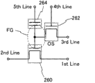
图9A及图9B所示的半导体装置的下部具有使用第一半导体材料的晶体管260,上部具有使用第二半导体材料的晶体管262。可以将实施方式1所例示的晶体管适用于晶体管262。在本实施方式中示出作为晶体管262使用具有与实施方式1所示的晶体管150相同的结构的晶体管的例子。The semiconductor device shown in FIGS. 9A and 9B has a
层叠的晶体管260的半导体材料及结构既可以与晶体管262的半导体材料及结构相同也可以不同。在本实施方式中示出分别使用具有适于存储介质(存储元件)的电路的材料及结构的晶体管的例子,作为第一半导体材料使用氧化物半导体以外的半导体材料,而作为第二半导体材料使用氧化物半导体。作为氧化物半导体以外的半导体材料,例如可以使用硅、锗、硅锗、碳化硅或砷化镓等,优选使用单晶半导体。另外,也可以使用有机半导体材料等。使用这种半导体材料的晶体管容易进行高速工作。另一方面,使用氧化物半导体的晶体管由于其特性而能够长时间地保持电荷。The semiconductor material and structure of the stacked
晶体管260包括:设置在包含半导体材料(例如,硅等)的衬底285中的沟道形成区216;夹着沟道形成区216地设置的杂质区220;与杂质区220接触的金属化合物区224;设置在沟道形成区216上的栅极绝缘膜208;以及设置在栅极绝缘膜208上的栅电极层210。The
作为包含半导体材料的衬底285,可以使用硅或碳化硅等单晶半导体衬底、多晶半导体衬底、硅锗等的化合物半导体衬底或SOI衬底等。另外,一般来说,“SOI衬底”是指在绝缘表面上设置有硅半导体膜的衬底。但是,在本说明书等中“SOI衬底”还包括在绝缘表面上设置有包含硅以外的材料的半导体膜的衬底。也就是说,“SOI衬底”所具有的半导体膜不局限于硅半导体膜。另外,SOI衬底还包括在玻璃衬底等绝缘衬底上隔着绝缘膜设置有半导体膜的衬底。As the
作为SOI衬底的制造方法,可以使用以下方法:通过对镜面抛光薄片注入氧离子之后进行高温加热来离表面有一定深度的区域中形成氧化层,并消除产生在表面层中的缺陷;通过热处理使照射氢离子来形成的微孔生长来将半导体衬底劈开的方法;或在绝缘表面上通过结晶生长形成单晶半导体膜的方法等。As a method for manufacturing an SOI substrate, the following methods can be used: by implanting oxygen ions into a mirror-polished wafer and then heating at a high temperature to form an oxide layer in a region having a certain depth from the surface, and eliminating defects generated in the surface layer; A method of cleaving a semiconductor substrate by growing micropores formed by irradiating hydrogen ions; or a method of forming a single crystal semiconductor film by crystal growth on an insulating surface.
例如,从单晶半导体衬底的一个面添加离子,来在离单晶半导体衬底的一个面有一定深度的区域中形成脆化层,而在单晶半导体衬底的一个面上和元件衬底上中的任一方形成绝缘膜。在单晶半导体衬底与元件衬底夹着绝缘膜重叠的状态下进行热处理来使脆化层中产生裂缝而在脆化层处分开单晶半导体衬底,从而从单晶半导体衬底将用作半导体膜的单晶半导体膜形成到元件衬底上。另外,也可以适用使用上述方法制造的SOI衬底。For example, adding ions from one side of the single crystal semiconductor substrate to form an embrittlement layer in a region having a certain depth from one side of the single crystal semiconductor substrate, and forming an embrittlement layer on one side of the single crystal semiconductor substrate and the element substrate An insulating film is formed on either of the bottom and the top. Heat treatment is performed in a state where the single crystal semiconductor substrate and the element substrate are overlapped with an insulating film to generate cracks in the embrittlement layer and separate the single crystal semiconductor substrate at the embrittlement layer, thereby separating the single crystal semiconductor substrate from the single crystal semiconductor substrate. A single crystal semiconductor film serving as a semiconductor film is formed on the element substrate. In addition, an SOI substrate produced by the above method can also be applied.
在衬底285上以围绕晶体管260的方式设置有元件分离绝缘膜206。另外,为了实现高集成化,如图9A所示,优选采用晶体管260不具有侧壁绝缘膜的结构。另一方面,在重视晶体管260的特性的情况下,也可以在栅电极层210的侧面设置侧壁绝缘膜,并设置包括杂质浓度不同的区域的杂质区220。An element
使用单晶半导体衬底的晶体管260能够进行高速工作。因此,通过使用该晶体管作为读出用的晶体管,可以高速地进行信息的读出。The
在本实施方式中以覆盖晶体管260的方式形成两层绝缘膜。另外,覆盖晶体管260的绝缘膜可以采用单层结构或三层以上的叠层结构。但是,作为接触于包括在设置于上部的晶体管262中的氧化物半导体层的绝缘膜,使用氧化硅膜。In this embodiment mode, two insulating films are formed to cover the
作为形成晶体管262和电容元件264之前的处理,对该两个绝缘膜进行CMP处理来形成平坦化的绝缘膜228及绝缘膜230,同时使栅电极层210的上面露出。As a process before forming the
作为绝缘膜228、绝缘膜230,典型地可以使用氧化硅膜、氧氮化硅膜、氧化铝膜、氧氮化铝膜、氮化硅膜、氮化铝膜、氮氧化硅膜、氮氧化铝膜等无机绝缘膜。绝缘膜228、绝缘膜230可以使用等离子体CVD法或溅射法等形成。As the insulating
另外,可以使用聚酰亚胺、丙烯酸树脂、苯并环丁烯类树脂等有机材料。另外,除了上述有机材料以外,也可以使用低介电常数材料(low-k材料)等。在使用有机材料时,也可以使用旋涂法、印刷法等湿法形成绝缘膜228、绝缘膜230。In addition, organic materials such as polyimide, acrylic resin, and benzocyclobutene-based resin can be used. In addition, in addition to the above-mentioned organic materials, low dielectric constant materials (low-k materials) and the like can also be used. When an organic material is used, the insulating
在本实施方式中作为绝缘膜228利用溅射法形成50nm厚的氧氮化硅膜,并且作为绝缘膜230利用溅射法形成550nm厚的氧化硅膜。In this embodiment, a silicon oxynitride film with a thickness of 50 nm is formed as the insulating
然后,在通过CMP处理充分实现了平坦化的绝缘膜230上形成氧化物半导体层,并且将其加工来形成岛状氧化物半导体层244。另外,优选在形成氧化物半导体层之后进行用于脱水化或脱氢化的热处理。Then, an oxide semiconductor layer is formed on the insulating
接着,在栅电极层210、绝缘膜228、绝缘膜230等上形成导电层,对该导电层选择性地进行蚀刻来形成源电极层或漏电极层242a、漏电极层或源电极层242b。Next, a conductive layer is formed on the
导电层可以利用如溅射法等的PVD法或如等离子体CVD法等的CVD法形成。此外,作为导电层的材料,可以使用选自Al、Cr、Cu、Ta、Ti、Mo、W中的元素或以上述元素为成分的合金等。也可以使用选自Mn、Mg、Zr、Be、Nd、Sc中的一种或多种的材料。The conductive layer can be formed by a PVD method such as a sputtering method or a CVD method such as a plasma CVD method. In addition, as a material of the conductive layer, an element selected from Al, Cr, Cu, Ta, Ti, Mo, and W, or an alloy containing the above elements as components, or the like can be used. One or more materials selected from Mn, Mg, Zr, Be, Nd, and Sc may also be used.
导电层既可以采用单层结构又可以采用两层以上的叠层结构。例如,可以举出钛膜或氮化钛膜的单层结构;含有硅的铝膜的单层结构;在铝膜上层叠钛膜的双层结构;在氮化钛膜上层叠钛膜的双层结构;层叠钛膜、铝膜及钛膜的三层结构等。另外,当作为导电层采用钛膜或氮化钛膜的单层结构时,存在容易将该导电层加工为具有锥形形状的源电极层或漏电极层242a及漏电极层或源电极层242b的优点。The conductive layer can adopt either a single-layer structure or a laminated structure of more than two layers. For example, a single-layer structure of a titanium film or a titanium nitride film; a single-layer structure of an aluminum film containing silicon; a double-layer structure of laminating a titanium film on an aluminum film; a double-layer structure of laminating a titanium film on a titanium nitride film; Layer structure; three-layer structure of laminated titanium film, aluminum film and titanium film, etc. In addition, when a single-layer structure of a titanium film or a titanium nitride film is used as the conductive layer, there is a possibility of easily processing the conductive layer into the source electrode layer or
上部晶体管262的沟道长度(L)由源电极层或漏电极层242a的下端部与漏电极层或源电极层242b的下端部之间的间隔而决定。另外,在形成沟道长度(L)短于25nm的晶体管的情况下,当进行用来形成掩模的曝光时,优选使用波长极短,即几nm至几十nm的超紫外线(Extreme Ultraviolet)。The channel length (L) of the
形成接触于氧化物半导体层244的一部分的栅极绝缘膜246。作为栅极绝缘膜246,可以通过等离子体CVD法或溅射法等形成氧化硅膜、氮化硅膜、氧氮化硅膜、氮氧化硅膜、氧化铝膜、氮化铝膜、氧氮化铝膜、氮氧化铝膜、氧化铪膜或氧化镓膜。A
在栅极绝缘膜246上的与氧化物半导体层244重叠的区域中形成栅电极层248a,并且在与源电极层或漏电极层242a重叠的区域中形成电极层248b。A
栅电极层248a及电极层248b可以通过在栅极绝缘膜246上形成导电层之后对该导电层进行选择性地蚀刻来形成。The
可以在栅电极层248a形成之后进行对氧化物半导体层244添加杂质元素的处理。The process of adding an impurity element to the
作为添加的杂质元素有磷、硼、氩等。另外,作为对氧化物半导体层244添加杂质元素的方法,可以采用离子掺杂法或离子注入法。The impurity elements to be added include phosphorus, boron, argon, and the like. In addition, as a method of adding an impurity element to the
另外,可以多次进行对氧化物半导体层244添加杂质元素的处理。当多次进行对氧化物半导体层244添加杂质元素的处理时,杂质元素既可以在多次中都使用相同的杂质元素,也可以在每次处理时改变杂质元素。In addition, the process of adding an impurity element to the
在对氧化物半导体层244添加杂质元素时,栅电极层248a用作掩模,杂质元素没有被添加到氧化物半导体层244中的与栅电极层248a重叠的区域而形成第一区域244a。另外,与栅电极层248a重叠的第一区域244a用作沟道形成区。When the impurity element is added to the
并且,添加有杂质元素的第二区域244b、第二区域244c由于杂质元素添加的损伤而使结晶性降低而成为非晶区。通过调节添加杂质元素的量等,可以降低损伤量而不使其完全成为非晶区。也就是说,添加有杂质元素的第二区域244b、第二区域244c成为非晶区比例至少比第一区域244a的非晶区比例大的区域。不使其完全成为非晶区能够更容易地利用后面进行的热处理使其晶化,所以是优选的。In addition, the
一对第二区域244b、第二区域244c用作比第一区域244a电阻低的LDD(Lightly Doped Drain:轻掺杂漏)区域。通过设置用作LDD区域的含有杂质元素的第二区域244b、第二区域244c,可以缓和施加到第一区域244a的端部的电场。由此,可以抑制晶体管的短沟道效果。A pair of
如此,通过以栅电极层248a为掩模,对氧化物半导体层244添加杂质元素,并进行后面的热处理,可以以自对准的方式形成成为沟道形成区的第一区域244a以及成为LDD区域的一对第二区域244b、第二区域244c。In this way, by adding an impurity element to the
在氧化物半导体层244、栅极绝缘膜246、栅电极层248a及电极层248b上形成包括氧化铝膜的绝缘膜250。在绝缘膜250为叠层结构的情况下,也可以使用通过等离子体CVD法或溅射法等形成的氧化硅膜、氮化硅膜、氧氮化硅膜、氮氧化硅膜、氮化铝膜、氧氮化铝膜、氮氧化铝膜、氧化铪膜或氧化镓膜与氧化铝膜的叠层。An insulating
在形成绝缘膜250之后进行第二热处理。优选将该热处理的温度设定为350℃以上且650℃以下,更优选设定为450℃以上且650℃以下。另外,优选设定为低于衬底的应变点。另外,第二热处理的时序不局限于本实施方式的结构,但是该热处理需要至少在形成绝缘膜250(更具体地,氧化铝膜)之后进行。这是因为如下缘故:用作绝缘膜250的氧化铝膜具有高遮断效果(阻挡效果),即不使氢、水等杂质及氧的双方透过膜的效果,因此通过在形成绝缘膜250之后进行热处理,可以防止从氧化物半导体层244释放氧。The second heat treatment is performed after the insulating
在晶体管262及绝缘膜250上形成绝缘膜252。绝缘膜252可以使用溅射法或CVD法等形成。另外,也可以使用含有氧化硅、氧氮化硅、氮化硅、氧化铪、氧化铝等无机绝缘材料的材料形成。The insulating
在栅极绝缘膜246、绝缘膜250及绝缘膜252中形成到达漏电极层或源电极层242b的开口。通过使用掩模等选择性地进行蚀刻来形成该开口。An opening reaching the drain electrode layer or the
然后,在上述开口中形成接触于漏电极层或源电极层242b的布线256。另外,图9A不示出漏电极层或源电极层242b与布线256的连接部分。Then, a
布线256在使用溅射法等的PVD法或等离子体CVD法等的CVD法形成导电层之后对该导电层进行蚀刻加工来形成。另外,作为导电层的材料,可以使用选自Al、Cr、Cu、Ta、Ti、Mo、W中的元素或以上述元素为成分的合金等。也可以使用选自Mn、Mg、Zr、Be、Nd、Sc中的任一种或多种的材料。详细内容与源电极层或漏电极层242a等相同。The
通过上述工序制造晶体管262及电容元件264。晶体管262具有含有填补氧缺损的过剩的氧的氧化物半导体层244。因此,晶体管262得到抑制电特性变动并在电性上稳定。电容元件264具有源电极层或漏电极层242a、氧化物半导体层244、栅极绝缘膜246及电极层248b。The
另外,在图9A至图9C所示的电容元件264中,通过层叠氧化物半导体层244与栅极绝缘膜246,可以充分确保源电极层或漏电极层242a与电极层248b之间的绝缘性。当然,为了确保足够的电容,也可以采用不设置氧化物半导体层244的结构的电容元件264。另外,还可以采用具有绝缘膜的结构的电容元件264。并且,在不需要电容器的情况下,也可以采用不设置电容元件264的结构。In addition, in the
图9C示出将上述半导体装置用作存储元件时的电路图的一个例子。在图9C中,晶体管262的源电极层和漏电极层中的一方与电容元件264的电极层的一方与晶体管260的栅电极层电连接。另外,第一布线(1st Line:也称为源极线)与晶体管260的源电极层电连接,第二布线(2nd Line:也称为位线)与晶体管260的漏电极层电连接。另外,第三布线(3rd Line:也称为第一信号线)与晶体管262的源电极层和漏电极层中的另一方电连接,并且第四布线(4th Line:也称为第二信号线)与晶体管262的栅电极层电连接。并且,第五布线(5th Line:也称为字线)与电容元件264的电极层的另一方电连接。FIG. 9C shows an example of a circuit diagram when the above semiconductor device is used as a memory element. In FIG. 9C , one of the source electrode layer and the drain electrode layer of the
由于使用氧化物半导体的晶体管262的截止电流极小,所以通过使晶体管262处于截止状态,可以极长时间地保持晶体管262的源电极层和漏电极层中的一方与电容元件264的电极层的一方与晶体管260的栅电极层电连接的节点(以下,节点FG)的电位。此外,通过具有电容元件264,可以容易保持施加到节点FG的电荷,并且,可以容易读出所保持的信息。Since the off-state current of the
在使半导体装置存储信息时(写入),首先,将第四布线的电位设定为使晶体管262成为导通状态的电位,来使晶体管262处于导通状态。由此,第三布线的电位被供给到节点FG,由此节点FG积蓄所定量的电荷。这里,施加赋予两种不同电位电平的电荷(以下,称为低(Low)电平电荷、高(High)电平电荷)中的任一种。然后,通过将第四布线的电位设定为使晶体管262成为截止状态的电位来使晶体管262处于截止状态,节点FG变为浮动状态,从而节点FG处于保持所定的电荷的状态。如上所述,通过使节点FG积蓄并保持所定量的电荷,可以使存储单元存储信息。When causing the semiconductor device to store information (writing), first, the potential of the fourth wiring is set to a potential for turning on the
因为晶体管262的截止电流极小,所以供给到节点FG的电荷被长时间地保持。因此,不需要刷新工作或者可以使刷新工作的频度变为极低,从而可以充分降低耗电量。此外,即使没有电力供给,也可以在较长期间内保持存储内容。Since the off current of the
在读出所存储的信息的情况(读出)下,当在对第一布线供给所定的电位(恒定电位)的状态下对第五布线施加适当的电位(读出电位)时,对应于保持于节点FG的电荷量而晶体管260处于不同的状态。这是因为如下缘故:通常,在晶体管260是n沟道型时,节点FG保持High电平电荷时的晶体管260的外观阈值Vth_H低于节点FG保持Low电平电荷时的晶体管260的外观阈值Vth_L。在此,外观阈值是指为了使晶体管260处于“导通状态”而需要的第五布线的电位。因此,通过将第五布线的电位设定为Vth_H与Vth_L之间的电位V0,可以辨别节点FG所保持的电荷。例如,在写入中在被施加High电平电荷的情况下,当第五布线的电位为V0(>Vth_H)时,晶体管260处于“导通状态”。在被施加Low电平电荷的情况下,即使第五布线的电位为V0(<Vth_L),晶体管260也保持“截止状态”。由此,通过控制第五布线的电位来读出晶体管260的导通状态或截止状态(读出第二布线的电位),可以读出所存储的信息。In the case of reading the stored information (reading), when an appropriate potential (read potential) is applied to the fifth wiring in a state where a predetermined potential (constant potential) is supplied to the first wiring, the corresponding voltage is held at the node. The amount of charge of FG while
此外,当重写所存储的信息时,通过对利用上述写入保持所定量的电荷的节点FG供给新电位,来使节点FG保持有关新信息的电荷。具体而言,将第四布线的电位设定为使晶体管262处于导通状态的电位,来使晶体管262处于导通状态。由此,第三布线的电位(有关新信息的电位)供给到节点FG,节点FG积蓄所定量的电荷。然后,通过将第四布线的电位设定为使晶体管262处于截止状态的电位,来使晶体管262处于截止状态,从而使节点FG保持有关新信息的电荷。也就是说,通过在利用第一写入使节点FG保持所定量的电荷的状态下,进行与第一写入相同的工作(第二写入),可以重写存储的信息。Also, when the stored information is rewritten, by supplying a new potential to the node FG holding a predetermined amount of charge by the above-mentioned writing, the node FG holds charges related to new information. Specifically, the potential of the fourth wiring is set to a potential at which the
本实施方式所示的晶体管262通过使用包含过剩的氧的氧化物半导体层作为氧化物半导体层244,可以充分降低晶体管262的截止电流。并且,通过使用这种晶体管,可以得到能够在极长期间内保持存储内容的半导体装置。The
如上所述,通过在氧化物半导体层上形成氧化铝膜,即使在具有层叠多个晶体管的集成电路的半导体装置的制造工序中进行热处理,也可以防止来自大气的水或氢侵入且扩散到氧化物半导体层。由此,晶体管的电特性变动得到抑制而在电性上稳定。因此,通过使用该晶体管,可以提供可靠性高的半导体装置。As described above, by forming an aluminum oxide film on the oxide semiconductor layer, even if heat treatment is performed in the manufacturing process of a semiconductor device having an integrated circuit stacked with a plurality of transistors, it is possible to prevent water or hydrogen from the atmosphere from entering and diffusing into the oxide semiconductor layer. material semiconductor layer. As a result, fluctuations in the electrical characteristics of the transistor are suppressed and the transistor is electrically stable. Therefore, by using this transistor, a highly reliable semiconductor device can be provided.
本实施方式所示的结构、方法等可以与其他实施方式所示的结构、方法等适当地组合而使用。The structure, method, etc. shown in this embodiment mode can be used in combination with the structure, method, etc. shown in other embodiment mode as appropriate.
实施方式5Embodiment 5
可以将本说明书所公开的半导体装置应用于多种电子设备(包括游戏机)。作为电子设备,例如可以举出电视装置(也称为电视或电视接收机)、用于计算机等的显示器、数码相机、数码摄像机等影像拍摄装置、数码相框、移动电话机(也称为手机、移动电话装置)、便携式游戏机、移动信息终端、声音再现装置、弹子机等大型游戏机等。以下,对具备在上述实施方式中说明的半导体装置的电子设备的例子进行说明。The semiconductor device disclosed in this specification can be applied to various electronic devices (including game machines). Examples of electronic equipment include television sets (also referred to as televisions or television receivers), monitors for computers, digital cameras, digital video cameras and other image capture devices, digital photo frames, mobile phones (also referred to as mobile phones, Mobile phone devices), portable game machines, mobile information terminals, sound reproduction devices, large game machines such as pinball machines, etc. Hereinafter, an example of electronic equipment including the semiconductor device described in the above-mentioned embodiments will be described.
图10A示出笔记本型个人计算机,包括主体3001、框体3002、显示部3003以及键盘3004等。通过将上述实施方式中的任一实施方式所示的半导体装置应用于显示部3003,可以提供可靠性高的笔记本型个人计算机。FIG. 10A shows a notebook personal computer including a
图10B示出便携式信息终端(PDA),在主体3021中设置有显示部3023、外部接口3025以及操作按钮3024等。另外,还具备操作个人数字助理的触屏笔3022。通过将上述实施方式中的任一实施方式所示的半导体装置应用于显示部3023,可以提供可靠性更高的便携式信息终端(PDA)。FIG. 10B shows a portable information terminal (PDA), and a
图10C示出电子书阅读器的一个例子。例如,电子书阅读器由两个框体,即框体2701及框体2703构成。框体2701及框体2703由轴部2711形成为一体,且可以以该轴部2711为轴进行开闭工作。通过采用这种结构,可以进行如纸的书籍那样的工作。FIG. 10C shows an example of an e-book reader. For example, an e-book reader is composed of two housings, that is, housing 2701 and housing 2703 . The frame body 2701 and the frame body 2703 are integrally formed by the shaft portion 2711, and can be opened and closed around the shaft portion 2711. By adopting such a structure, it is possible to perform work like a paper book.
框体2701组装有显示部2705,而框体2703组装有显示部2707。显示部2705及显示部2707的结构既可以是显示连屏画面的结构,又可以是显示不同的画面的结构。通过采用显示不同的画面的结构,例如可以在右边的显示部(图10C中的显示部2705)中显示文章而在左边的显示部(图10C中的显示部2707)中显示图像。通过将上述实施方式中的任一实施方式所示的半导体装置应用于显示部2705和显示部2707,可以提供可靠性高的电子书阅读器。当作为显示部2705使用半透过型或反射型液晶显示装置时,可以预料电子书阅读器在较明亮的情况下也被使用,因此也可以设置太阳电池而进行利用太阳电池的发电及利用电池的充电。另外,当作为电池使用锂离子电池时,有可以实现小型化等的优点。The housing 2701 is assembled with a display unit 2705 , and the housing 2703 is assembled with a display unit 2707 . The configurations of the display unit 2705 and the display unit 2707 may be configured to display a multi-screen screen, or may be configured to display different screens. By adopting a configuration to display different screens, for example, text can be displayed on the right display (display 2705 in FIG. 10C ) and images can be displayed on the left display (display 2707 in FIG. 10C ). By applying the semiconductor device described in any of the above-described embodiments to the display unit 2705 and the display unit 2707, a highly reliable e-book reader can be provided. When a transflective or reflective liquid crystal display device is used as the display unit 2705, it can be expected that the e-book reader will be used in a relatively bright situation, so it is also possible to install a solar cell to generate electricity using the solar cell and to use the battery to generate electricity. charging. In addition, when a lithium ion battery is used as a battery, there is an advantage that miniaturization and the like can be achieved.
此外,在图10C中示出框体2701具备操作部等的例子。例如,在框体2701中具备电源开关2721、操作键2723、扬声器2725等。利用操作键2723可以翻页。注意,在与框体的显示部相同的面上可以设置键盘、定位装置等。另外,也可以采用在框体的背面或侧面具备外部连接端子(耳机端子、USB端子等)、记录介质插入部等的结构。再者,电子书阅读器也可以具有电子词典的功能。In addition, FIG. 10C shows an example in which the housing 2701 includes an operation unit and the like. For example, a power switch 2721 , operation keys 2723 , a speaker 2725 , and the like are provided in the housing 2701 . Pages can be turned using the operation keys 2723 . Note that a keyboard, a pointing device, and the like may be provided on the same surface as the display portion of the housing. In addition, a configuration may be adopted in which external connection terminals (earphone terminal, USB terminal, etc.), recording medium insertion portion, etc. are provided on the back or side of the housing. Furthermore, the e-book reader can also have the function of an electronic dictionary.
此外,电子书阅读器也可以采用能够以无线的方式收发信息的结构。还可以采用以无线的方式从电子书阅读器服务器购买所希望的书籍数据等,然后下载的结构。In addition, the e-book reader may have a structure capable of transmitting and receiving information wirelessly. It is also possible to adopt a configuration in which desired book data and the like are purchased wirelessly from the e-book reader server and then downloaded.
图10D示出移动电话,由框体2800及框体2801的两个框体构成。框体2801具备显示面板2802、扬声器2803、麦克风2804、定位装置2806、影像拍摄用透镜2807、外部连接端子2808等。此外,框体2800具备对移动电话进行充电的太阳电池单元2810、外部储存槽2811等。另外,在框体2801内组装有天线。通过将上述实施方式中的任一实施方式所示的半导体装置应用于显示面板2802,可以提供可靠性高的移动电话。FIG. 10D shows a mobile phone composed of two housings: a housing 2800 and a housing 2801 . The housing 2801 includes a display panel 2802, a speaker 2803, a microphone 2804, a pointing device 2806, a camera lens 2807, an external connection terminal 2808, and the like. In addition, the housing 2800 includes a solar battery unit 2810 for charging a mobile phone, an external storage tank 2811 , and the like. In addition, an antenna is incorporated in the housing 2801 . By applying the semiconductor device described in any of the above-described embodiments to the display panel 2802, a highly reliable mobile phone can be provided.
另外,显示面板2802具备触摸屏,图10D使用虚线示出作为映像被显示出来的多个操作键2805。另外,还安装有用来将由太阳电池单元2810输出的电压升压到各电路所需的电压的升压电路。In addition, the display panel 2802 is provided with a touch panel, and Fig. 10D shows a plurality of operation keys 2805 displayed as images using dotted lines. In addition, a booster circuit for boosting the voltage output from the solar cell 2810 to a voltage required by each circuit is installed.
显示面板2802根据使用方式适当地改变显示的方向。另外,由于在与显示面板2802同一面上设置影像拍摄用透镜2807,所以可以实现可视电话。扬声器2803及麦克风2804不局限于音频通话,还可以进行可视通话、录音、再生等。再者,滑动框体2800和框体2801而可以处于如图10D那样的展开状态和重叠状态,所以可以实现适于携带的小型化。The display panel 2802 appropriately changes the direction of display according to the manner of use. In addition, since the image capturing lens 2807 is provided on the same surface as the display panel 2802, a videophone can be realized. The speaker 2803 and the microphone 2804 are not limited to audio calls, but can also perform visual calls, recording, playback, and the like. In addition, since the frame body 2800 and the frame body 2801 can be slid to be in the unfolded state and the overlapped state as shown in FIG. 10D , it is possible to realize miniaturization suitable for portability.
外部连接端子2808可以与AC适配器及各种电缆如USB电缆等连接,并可以进行充电及与个人计算机等的数据通讯。另外,通过将记录媒体插入到外部储存槽2811中,可以对应于更大量数据的保存及移动。The external connection terminal 2808 can be connected to an AC adapter and various cables such as a USB cable, and can perform charging and data communication with a personal computer or the like. In addition, by inserting a recording medium into the external storage slot 2811, it is possible to cope with storage and movement of a larger amount of data.
另外,也可以是除了上述功能以外还具有红外线通信功能、电视接收功能等的移动电话。In addition, a mobile phone having an infrared communication function, a television reception function, etc. in addition to the above-mentioned functions may be used.
图10E示出数码摄像机,其包括主体3051、显示部(A)3057、取景器3053、操作开关3054、显示部(B)3055以及电池3056等。通过将上述实施方式中的任一实施方式所示的半导体装置应用于显示部(A)3057及显示部(B)3055,可以提供可靠性高的数码摄像机。10E shows a digital video camera including a
图10F示出电视装置的一个例子。在电视装置中,框体9601组装有显示部9603。利用显示部9603可以显示映像。此外,在此示出利用支架9605支撑框体9601的结构。通过将上述实施方式中的任一实施方式所示的半导体装置应用于显示部9603,可以提供可靠性高的电视装置。FIG. 10F shows an example of a television set. In the television set, a
可以通过利用框体9601所具备的操作开关或另行提供的遥控操作机进行电视装置的操作。或者,也可以采用在遥控操作机中设置显示部的结构,该显示部显示从该遥控操作机输出的信息。The television apparatus can be operated by using the operation switches included in the
另外,电视装置采用具备接收机、调制解调器等的结构。可以通过利用接收机接收一般的电视广播。再者,通过调制解调器连接到有线或无线方式的通信网络,也可以进行单向(从发送者到接收者)或双向(在发送者和接收者之间或在接收者之间等)的信息通信。In addition, the television set has a configuration including a receiver, a modem, and the like. General TV broadcasts can be received by using a receiver. Furthermore, one-way (from sender to receiver) or two-way (between sender and receiver or between receivers, etc.) information communication is also possible by connecting a modem to a wired or wireless communication network.
本实施方式可以与其他实施方式所示的结构适当地组合而使用。This embodiment mode can be used in appropriate combination with the structures shown in other embodiment modes.
实施例1Example 1
在本实施例中,对在根据所公开的发明的半导体装置中使用的氧化铝膜的阻挡特性进行评价。图11A1至图14D示出其结果。作为评价方法,使用二次离子质谱分析法(SIMS:Secondary Ion MassSpectrometry)和TDS(Thermal Desorption Spectrometry:热脱附谱法)分析法。In this example, the barrier characteristics of the aluminum oxide film used in the semiconductor device according to the disclosed invention were evaluated. 11A1 to 14D show the results thereof. As evaluation methods, secondary ion mass spectrometry (SIMS: Secondary Ion Mass Spectrometry) and TDS (Thermal Desorption Spectrometry: Thermal Desorption Spectrometry) analysis methods were used.
首先,示出通过SIMS分析进行的评价。作为样品,制造两种样品:作为比较例,在玻璃衬底上通过溅射法形成100nm厚的氧化硅膜而成的比较例样品A;作为实施例,在玻璃衬底上通过溅射法形成100nm厚的氧化硅膜并在氧化硅膜上通过溅射法形成100nm厚的氧化铝膜而成的实施例样品A。First, evaluation by SIMS analysis is shown. As samples, two types of samples were produced: as a comparative example, a comparative example sample A formed by forming a silicon oxide film with a thickness of 100 nm on a glass substrate by a sputtering method; as an example, a silicon oxide film formed by a sputtering method on a glass substrate Example sample A formed by forming a silicon oxide film with a thickness of 100 nm and an aluminum oxide film with a thickness of 100 nm by sputtering on the silicon oxide film.
作为比较例样品A及实施例样品A,以下示出氧化硅膜的成膜条件:作为靶材使用氧化硅(SiO2)靶材;玻璃衬底与靶材的距离为60mm;压力为0.4Pa;电源电力为1.5kW;氧(氧流量为50sccm)气氛下;以及衬底温度为100℃。As Comparative Example Sample A and Example Sample A, the film-forming conditions of the silicon oxide film are shown below: a silicon oxide (SiO 2 ) target is used as the target; the distance between the glass substrate and the target is 60 mm; and the pressure is 0.4 Pa. ; the power supply power was 1.5 kW; under an oxygen (oxygen flow rate: 50 sccm) atmosphere; and the substrate temperature was 100°C.
以下示出实施例样品A中的氧化铝膜的成膜条件:作为靶材使用氧化铝(Al2O3)靶材;玻璃衬底与靶材的距离为60mm;压力为0.4Pa;电源电力为1.5kW;氩及氧(氩流量为25sccm;氧流量为25sccm)气氛下;以及衬底温度为250℃。The film-forming conditions of the aluminum oxide film in the example sample A are shown below: an aluminum oxide (Al 2 O 3 ) target is used as the target; the distance between the glass substrate and the target is 60 mm; the pressure is 0.4 Pa; the power supply 1.5 kW; under the atmosphere of argon and oxygen (the flow rate of argon is 25 sccm; the flow rate of oxygen is 25 sccm); and the substrate temperature is 250°C.
对比较例样品A及实施例样品A进行压力锅测试(PCT:PressureCooker Test)。在本实施例中,作为PCT测试,在温度为130℃,湿度为85%(包含于气体中的水蒸气的体积比为H2O(水)∶D2O(重水)=3∶1),气压为2.3(0.23MPa)的条件下保持比较例样品A及实施例样品A100小时。A pressure cooker test (PCT: Pressure Cooker Test) was performed on the sample A of the comparative example and the sample A of the example. In this example, as a PCT test, at a temperature of 130° C. and a humidity of 85% (the volume ratio of water vapor contained in the gas is H2O (water): D2O (heavy water) = 3:1) , the air pressure is 2.3 (0.23MPa) under the condition of keeping comparative example sample A and
在本实施例中,以氘等表示的“D原子”表示质量数为2的氢原子(2H)。In this example, "D atom" represented by deuterium or the like represents a hydrogen atom ( 2 H) having a mass number of 2.
作为SIMS分析,使用SSDP(Substrate Side Depth Profile)-SIMS来测定PCT测试前和PCT测试后的比较例样品A及实施例样品A的H原子及D原子的浓度。As SIMS analysis, SSDP (Substrate Side Depth Profile)-SIMS was used to measure the concentrations of H atoms and D atoms in Comparative Example Sample A and Example Sample A before and after the PCT test.
图11A1及图11A2示出利用SIMS测定的比较例样品A中的H原子及D原子的浓度分布,其中图11A1为PCT测试前的浓度分布,而图11A2为PCT测试后的浓度分布。在图11A1及图11A2中,D原子期望分布是以D原子的存在比为0.015%来根据H原子的分布算出的存在于自然界的D原子的浓度分布。因此,因PCT测试而混入到样品中的D原子量为实际测定的D原子浓度与D原子期望浓度的差。图11B1及图11B2示出从实际测定的D原子浓度减去D原子期望浓度的D原子的浓度分布,其中图11B1为PCT测试前的浓度分布,而图11B2为PCT测试后的浓度分布。11A1 and 11A2 show the concentration distributions of H atoms and D atoms in comparative sample A measured by SIMS, wherein FIG. 11A1 is the concentration distribution before the PCT test, and FIG. 11A2 is the concentration distribution after the PCT test. In FIG. 11A1 and FIG. 11A2 , the desired distribution of D atoms is the concentration distribution of D atoms present in nature calculated from the distribution of H atoms with the abundance ratio of D atoms being 0.015%. Therefore, the amount of D atoms mixed into the sample by the PCT test is the difference between the actually measured D atom concentration and the D atom expected concentration. 11B1 and 11B2 show the concentration distribution of D atoms subtracted from the actual measured D atom concentration by subtracting the expected concentration of D atoms, wherein FIG. 11B1 is the concentration distribution before the PCT test, and FIG. 11B2 is the concentration distribution after the PCT test.
同样地,图12A1及图12A2示出利用SIMS测定的实施例样品A中的H原子及D原子的浓度分布,其中图12A1为PCT测试前的浓度分布,而图12A2为PCT测试后的浓度分布。另外,图12B1及图12B2示出从实际测定的D原子浓度减去D原子期望浓度的D原子的浓度分布,其中图12B1为PCT测试前的浓度分布,而图12B2为PCT测试后的浓度分布。Similarly, Figure 12A1 and Figure 12A2 show the concentration distribution of H atoms and D atoms in the sample A of the embodiment measured by SIMS, wherein Figure 12A1 is the concentration distribution before the PCT test, and Figure 12A2 is the concentration distribution after the PCT test . In addition, FIG. 12B1 and FIG. 12B2 show the concentration distribution of D atoms minus the expected concentration of D atoms from the actual measured concentration of D atoms, wherein FIG. 12B1 is the concentration distribution before the PCT test, and FIG. 12B2 is the concentration distribution after the PCT test .
另外,本实施例的SIMS分析结果都示出使用氧化硅膜的标准样品来定量的结果。In addition, all the SIMS analysis results in this example show quantitative results using a standard sample of the silicon oxide film.
如图11A1至图11B2所示,在PCT测试之前实际测定的D原子的浓度分布与D原子期望分布重叠,而在PCT测试之后实际测定的D原子的浓度分布增大成高浓度,由此可知D原子混入到氧化硅膜中。因此,可以确认到,比较例样品A的氧化硅膜对来自外部的水(H2O、D2O)具有低阻挡性。As shown in Figure 11A1 to Figure 11B2, the concentration distribution of D atoms actually measured before the PCT test overlaps with the expected distribution of D atoms, while the concentration distribution of D atoms actually measured after the PCT test increases to a high concentration, so it can be known that D Atoms are mixed into the silicon oxide film. Therefore, it can be confirmed that the silicon oxide film of Comparative Example A has low barrier properties to water (H 2 O, D 2 O) from the outside.
另一方面,如图12A1至图12B2所示,在将氧化铝膜层叠在氧化硅膜上的实施例样品A中,在PCT测试后D原子也只侵入到氧化铝膜表面,而不侵入到离氧化铝膜表面有深于50nm左右的区域及氧化硅膜。由此,可以确认到,氧化铝膜对来自外部的水(H2O、D2O)具有高阻挡性。On the other hand, as shown in FIGS. 12A1 to 12B2, in Example sample A in which an aluminum oxide film is laminated on a silicon oxide film, D atoms only intrude into the surface of the aluminum oxide film after the PCT test, but not into There is a region deeper than about 50nm from the surface of the aluminum oxide film and the silicon oxide film. From this, it was confirmed that the aluminum oxide film has a high barrier property against water (H 2 O, D 2 O) from the outside.
接着,示出通过TDS分析进行的评价。作为实施例,制造如下实施例样品B,即在该实施例样品B中在玻璃衬底上通过溅射法形成有100nm厚的氧化硅膜,且在氧化硅膜上通过溅射法形成有20nm厚的氧化铝膜。另外,作为比较例,制造如下比较例样品B,即在通过TDS分析测定实施例样品B之后,从实施例样品B去除氧化铝膜,来形成在玻璃衬底上只形成有氧化硅膜的比较例样品B。Next, evaluation by TDS analysis is shown. As an example, an example sample B in which a 100 nm thick silicon oxide film was formed by a sputtering method on a glass substrate and a 20 nm thick silicon oxide film was formed by a sputtering method on a glass substrate was produced. thick aluminum oxide film. In addition, as a comparative example, a comparative example sample B in which only a silicon oxide film was formed on a glass substrate by removing the aluminum oxide film from the example sample B after measuring the example sample B by TDS analysis was produced. Example Sample B.
作为比较例样品B及实施例样品B中的氧化硅膜的形成条件,采用如下条件:作为靶材使用氧化硅(SiO2)靶材;玻璃衬底与靶材的距离为60mm;压力为0.4Pa;电源电力为1.5kW;氧(氧流量为50sccm)气氛下;以及衬底温度为100℃。As the conditions for forming the silicon oxide film in Comparative Example B and Example B, the following conditions are adopted: a silicon oxide (SiO 2 ) target is used as the target; the distance between the glass substrate and the target is 60 mm; the pressure is 0.4 Pa; power supply power of 1.5 kW; under oxygen (oxygen flow rate of 50 sccm) atmosphere; and substrate temperature of 100°C.
在实施例样品B中,作为氧化铝膜的形成条件,采用如下条件:作为靶材使用氧化铝(Al2O3)靶材;玻璃衬底与靶材的距离为60mm;压力为0.4Pa;电源电力为1.5kW;氩及氧(氩流量为25sccm:氧流量为25sccm)气氛下;以及衬底温度为250℃。In example sample B, as the conditions for forming the aluminum oxide film, the following conditions are adopted: an aluminum oxide (Al 2 O 3 ) target is used as the target; the distance between the glass substrate and the target is 60 mm; the pressure is 0.4 Pa; The power supply was 1.5 kW; in the atmosphere of argon and oxygen (argon flow rate: 25 sccm: oxygen flow rate: 25 sccm); and substrate temperature was 250°C.
分别在300℃的加热处理、450℃的加热处理、600℃的加热处理的条件下,在氮气氛下对比较例样品B及实施例样品B进行1小时的处理。The comparative example sample B and the example sample B were processed in a nitrogen atmosphere for 1 hour under the conditions of heat treatment at 300°C, heat treatment at 450°C, and heat treatment at 600°C, respectively.
对分别在不进行加热处理、300℃的加热处理、450℃的加热处理、600℃的加热处理的4个条件下制造的比较例样品B及实施例样品B进行TDS分析。图13A至图14D示出测定比较例样品B及实施例样品B来得到的M/z=32(O2)的TDS结果,其中图13A及图14A示出对比较例样品B及实施例样品B不进行加热处理时的TDS结果,图13B及图14B示出对比较例样品B及实施例样品B进行300℃的加热处理时的TDS结果,图13C及图14C示出对比较例样品B及实施例样品B进行450℃的加热处理时的TDS结果,而图13D及图14D示出对比较例样品B及实施例样品B进行600℃的加热处理时的TDS结果。TDS analysis was performed on the comparative example sample B and the example sample B produced under the four conditions of no heat treatment, 300°C heat treatment, 450°C heat treatment, and 600°C heat treatment, respectively. 13A to 14D show the TDS results of M/z=32 (O 2 ) obtained by measuring the sample B of the comparative example and the sample B of the embodiment. The TDS result when B is not subjected to heat treatment, Fig. 13B and Fig. 14B show the TDS result when the comparative example sample B and the embodiment sample B are carried out 300 ℃ of heat treatment, Fig. 13C and Fig. 14C show the comparison example sample B 13D and FIG. 14D show the TDS results when the sample B of the comparative example and the sample B of the example were subjected to the heat treatment at 600°C.
如图13A至图13D所示,作为比较例样品B,在不进行加热处理的图13A中从氧化硅膜释放氧,但是在进行300℃的加热处理的图13B中氧释放量大幅度地减少,而在进行450℃的加热处理的图13C及进行600℃的加热处理的图13D中氧放出量为TDS测定的背景值以下。As shown in FIGS. 13A to 13D , as Comparative Example B, oxygen is released from the silicon oxide film in FIG. 13A without heat treatment, but the amount of oxygen release is greatly reduced in FIG. 13B where heat treatment at 300° C. is performed. , while in FIG. 13C where the heat treatment was performed at 450° C. and in FIG. 13D where the heat treatment was performed at 600° C., the amount of oxygen released was below the background value of the TDS measurement.
根据图13A至图13D的结果可知,包含在氧化硅膜中的过剩的氧中的9成以上通过300℃的加热处理从氧化硅膜中释放到外部,而包含在氧化硅膜中的几乎所有过剩的氧通过450℃、600℃的加热处理释放到氧化硅膜的外部。由此,可以确认到氧化硅膜对氧具有低阻挡性。From the results of FIGS. 13A to 13D, it can be seen that more than 90% of the excess oxygen contained in the silicon oxide film is released from the silicon oxide film to the outside by the heat treatment at 300°C, and almost all of the oxygen contained in the silicon oxide film Excess oxygen is released to the outside of the silicon oxide film by heat treatment at 450°C and 600°C. From this, it was confirmed that the silicon oxide film has a low barrier property to oxygen.
另一方面,如图14A至图14D所示,作为将氧化铝膜形成在氧化硅膜上的实施例样品B,在进行300℃、450℃、600℃的加热处理的样品也释放与不进行加热处理时同等的量的氧。On the other hand, as shown in FIG. 14A to FIG. 14D , as the example sample B in which the aluminum oxide film is formed on the silicon oxide film, samples subjected to heat treatment at 300°C, 450°C, and 600°C also released and did not undergo heat treatment. The same amount of oxygen as in the heat treatment.
根据图14A至图14D的结果可知,通过将氧化铝膜形成在氧化硅膜上,即使进行加热处理,包含在氧化硅膜中的过剩的氧也不易释放到外部,而极长时间地保持在氧化硅膜中含有氧的状态。由此可以确认到,氧化铝膜对氧具有高阻挡性。From the results shown in FIGS. 14A to 14D, it can be seen that by forming the aluminum oxide film on the silicon oxide film, even if heat treatment is performed, the excess oxygen contained in the silicon oxide film is not easily released to the outside, and remains in the silicon oxide film for an extremely long time. A state in which oxygen is contained in the silicon oxide film. From this, it was confirmed that the aluminum oxide film has a high barrier property to oxygen.
根据上述结果可以确认到,氧化铝膜对氢及水具有阻挡性并对氧具有阻挡性,因此可以适用于阻挡氢、水及氧的阻挡膜。From the above results, it was confirmed that the aluminum oxide film has barrier properties against hydrogen and water, and has barrier properties against oxygen, and thus can be suitably used as a barrier film for blocking hydrogen, water, and oxygen.
因此,由于氧化铝膜用作阻挡膜,所以在依次形成氧化物半导体层、源电极层、漏电极层、栅极绝缘膜、栅电极层之后,在栅极绝缘膜及栅电极层上以与其接触的方式形成氧化铝膜的晶体管的制造工序中及制造后,可以防止氢、水等杂质混入氧化物半导体层并防止构成氧化物半导体的主要成分材料的氧从氧化物半导体层释放。Therefore, since the aluminum oxide film is used as a barrier film, after forming an oxide semiconductor layer, a source electrode layer, a drain electrode layer, a gate insulating film, and a gate electrode layer in this order, on the gate insulating film and the gate electrode layer, a During and after the production process of the transistor in which the aluminum oxide film is formed in contact, it is possible to prevent impurities such as hydrogen and water from being mixed into the oxide semiconductor layer and to prevent oxygen, which is a main component material of the oxide semiconductor, from being released from the oxide semiconductor layer.
实施例2Example 2
在本实施例中,对所公开的发明的半导体装置中的将氧化铝膜作为阻挡膜的晶体管特性的测量结果进行说明。In this example, measurement results of transistor characteristics using an aluminum oxide film as a barrier film in the semiconductor device of the disclosed invention will be described.
首先,对实施例样品C的晶体管的制造方法进行说明。First, a method of manufacturing the transistor of Example Sample C will be described.
在硅衬底上利用溅射法形成300nm厚的为基底绝缘膜的氧化硅层。作为基底绝缘膜的氧化硅层的成膜条件,采用如下条件:作为靶材使用氧化硅(SiO2)靶材;在玻璃衬底与靶材的距离为60mm;压力为0.4Pa;电源电力为1.5kW;氧(氧流量50sccm)气氛下;衬底温度为100℃。A silicon oxide layer serving as a base insulating film was formed to a thickness of 300 nm by sputtering on a silicon substrate. The film-forming conditions of the silicon oxide layer as the base insulating film adopt the following conditions: a silicon oxide (SiO 2 ) target is used as the target; the distance between the glass substrate and the target is 60mm; the pressure is 0.4Pa; the power supply is 1.5kW; under oxygen (oxygen flow rate: 50sccm) atmosphere; substrate temperature: 100°C.
接着,在氧化硅层上形成20nm厚的为氧化物半导体层的In-Ga-Zn-O类氧化物半导体。作为氧化物半导体层In-Ga-Zn-O类氧化物半导体的成膜条件,采用如下条件:作为靶材使用In∶Ga∶Zn=1∶1∶1的靶材;压力为0.4Pa;电源电力为0.5kW;氩及氧(氩流量30sccm:氧流量15sccm)气氛下;衬底温度为250℃。Next, an In-Ga-Zn-O-based oxide semiconductor as an oxide semiconductor layer was formed to a thickness of 20 nm on the silicon oxide layer. As the film-forming conditions of the oxide semiconductor layer In-Ga-Zn-O-based oxide semiconductor, the following conditions are adopted: a target of In:Ga:Zn=1:1:1 is used as the target; the pressure is 0.4Pa; The electric power is 0.5kW; under the atmosphere of argon and oxygen (argon flow rate: 30 sccm: oxygen flow rate: 15 sccm); substrate temperature is 250°C.
接着,在形成氧化物半导体层之后,在减压状态下进行30分钟的400℃的热处理。Next, after forming the oxide semiconductor layer, heat treatment at 400° C. for 30 minutes was performed under reduced pressure.
然后,在氧化物半导体层上形成为源电极层及漏电极层的100nm厚的钨层,然后依次层叠地形成如下膜:利用CVD法在源电极层及漏电极层上形成30nm厚的成为栅极绝缘膜的氧氮化硅膜;在栅极绝缘膜上的与氧化物半导体层重叠的区域上形成15nm厚的成为栅电极层的氮化钽层;以及135nm厚的钨层。Then, a 100nm-thick tungsten layer is formed on the oxide semiconductor layer as the source electrode layer and the drain electrode layer, and then the following films are sequentially stacked and formed: a 30nm-thick tungsten layer is formed on the source electrode layer and the drain electrode layer by the CVD method. A silicon oxynitride film as an electrode insulating film; a 15 nm-thick tantalum nitride layer serving as a gate electrode layer; and a 135 nm-thick tungsten layer were formed on a region overlapping the oxide semiconductor layer on the gate insulating film.
接着,在加速电压为40kV、掺杂量为1×10¹⁵离子/cm2的条件下对氧化物半导体层添加磷,并在氮气氛下进行1个小时的450℃的热处理。Next, phosphorus was added to the oxide semiconductor layer under the conditions of an accelerating voltage of 40 kV and a doping amount of 1×10 15 ions/cm 2 , followed by heat treatment at 450° C. for 1 hour in a nitrogen atmosphere.
在添加完磷之后,利用溅射法在栅极绝缘膜及栅电极层上形成100nm厚的成为绝缘膜的氧化铝膜。作为氧化铝膜的成膜条件,采用如下条件:作为靶材使用氧化铝(Al2O3)靶材;衬底与靶材的距离为60mm;压力为0.4Pa;电源电力为1.5kW;氩及氧(氩流量25sccm:氧流量25sccm)气氛下;衬底温度为250℃。After phosphorus was added, an aluminum oxide film serving as an insulating film was formed to a thickness of 100 nm on the gate insulating film and the gate electrode layer by sputtering. As the film-forming conditions of the aluminum oxide film, the following conditions were adopted: an aluminum oxide (Al 2 O 3 ) target was used as the target; the distance between the substrate and the target was 60 mm; the pressure was 0.4 Pa; the power supply was 1.5 kW; and oxygen (
接着,利用CVD法在氧化铝膜上形成300nm厚的氧氮化硅膜作为实施例样品C。Next, a silicon oxynitride film having a thickness of 300 nm was formed on the aluminum oxide film as Example Sample C by CVD.
另外,对实施例样品C的晶体管与用来比较晶体管特性的比较例样品C的晶体管的制造方法进行说明。In addition, a method for manufacturing the transistor of the sample C of the example and the transistor of the sample C of the comparative example for comparing transistor characteristics will be described.
作为比较例样品C,到添加磷的工序为止与实施例样品C同样地形成,其不同之处在于,比较例样品C在添加磷之后,利用CVD法在栅极绝缘膜及栅电极层上形成300nm厚的氧氮化硅膜。As a comparative example sample C, it was formed in the same manner as the example sample C up to the process of adding phosphorus. 300nm thick silicon oxynitride film.
比较例样品C及实施例样品C在450℃的热处理条件下,在氮气氛中进行一个小时的处理。The sample C of the comparative example and the sample C of the example were treated in a nitrogen atmosphere under the heat treatment condition of 450° C. for one hour.
在本实施例中,在比较例样品C及实施例样品C的晶体管中,在将漏极电压(Vd)设定为3V,将栅极电压(Vg)从-6V扫描到6V的情况下,进行了漏极电流(Id:[A])的测量。图15和图16示出测量结果。在图15及图16中,横轴为栅极电压(Vg[V]),纵轴为漏极电流(Id[A])。另外,“漏极电压(Vd)”是指以源极为基准的漏极与源极的电位差,“栅极电压(Vg)”是指以源极为基准的栅极与源极的电位差。In this example, in the case of setting the drain voltage (V d ) to 3V and sweeping the gate voltage (V g ) from -6V to 6V in the transistors of Comparative Example Sample C and Example Sample C Next, the measurement of the drain current (I d : [A]) was performed. 15 and 16 show the measurement results. In FIGS. 15 and 16 , the horizontal axis represents the gate voltage (V g [V]), and the vertical axis represents the drain current (I d [A]). In addition, "drain voltage (V d )" means the potential difference between the drain and the source based on the source, and "gate voltage (V g )" means the potential between the gate and the source based on the source. Difference.
如图15所示,在比较例样品C的晶体管中,即使对栅极电压进行扫描电流值也没有太大的变化。由此可以确认,比较例样品C的晶体管不能确保开关比,而不能得到正常的开关特性。As shown in FIG. 15 , in the transistor of Comparative Example C, the current value did not change much even if the gate voltage was scanned. From this, it was confirmed that the transistor of Comparative Example Sample C could not secure the switching ratio, and could not obtain normal switching characteristics.
另一方面,如图16所示,可以确认实施例样品C的晶体管在导通状态时漏极电流(也称为导通电流)为10-6A,而在截止状态时漏极电流(也称为截止电流)为10-14A。由此可以确认,实施例样品C的晶体管能够确保开关比,而能够得到正常的开关特性。On the other hand, as shown in FIG. 16, it can be confirmed that the drain current (also referred to as on-current) of the transistor of Example C is 10-6 A in the on state, and the drain current (also referred to as on-current) in the off-state is 10-6 A, and that in the off-state (also referred to as Called the cut-off current) is 10 -14 A. From this, it can be confirmed that the transistor of the sample C of the example can secure the switching ratio and obtain normal switching characteristics.
实施例样品C与比较例样品C的不同之处在于形成氧氮化硅膜之前是否形成氧化铝膜。因此,可以确认在实施例样品C中由于氧化铝膜的效果晶体管的电特性变动得到抑制而在电性上稳定。Example Sample C differs from Comparative Example Sample C in whether or not an aluminum oxide film is formed before forming the silicon oxynitride film. Therefore, it was confirmed that in the example sample C, the variation in electrical characteristics of the transistor was suppressed due to the effect of the aluminum oxide film, and the transistor was electrically stable.
如实施例1所示,由于氧化铝膜适用于阻挡氢、水及氧的阻挡膜,通过采用覆盖氧化物半导体层在栅极绝缘膜及栅电极层上以与其接触的方式形成氧化铝膜的结构,即使在进行热处理的情况下,也可以防止氢或水混入氧化物半导体层或者氧从氧化物半导体层释出。通过上述结果可知,通过采用上述结构,即使对微型化的晶体管进行热处理也可以确保开关比,而能够获得正常的开关特性,晶体管的电特性变动得到抑制而在电性上稳定。As shown in Example 1, since the aluminum oxide film is suitable as a barrier film for blocking hydrogen, water, and oxygen, by using a cover oxide semiconductor layer to form the aluminum oxide film in contact with the gate insulating film and the gate electrode layer structure, it is possible to prevent the incorporation of hydrogen or water into the oxide semiconductor layer or the release of oxygen from the oxide semiconductor layer even in the case of heat treatment. From the above results, it can be seen that by adopting the above-mentioned structure, the on-off ratio can be ensured even when the miniaturized transistor is heat-treated, normal switching characteristics can be obtained, and the variation of the electrical characteristics of the transistor is suppressed and the transistor is electrically stable.
由此,具有该晶体管的使用氧化物半导体的半导体装置具有稳定的电特性而能够实现高可靠性。Accordingly, a semiconductor device using an oxide semiconductor including the transistor has stable electrical characteristics and can achieve high reliability.
符号说明Symbol Description
100 衬底100 Substrates
102 基底绝缘膜102 base insulating film
106 氧化半导体层106 oxide semiconductor layer
106a 第一区域106a First Zone
106b 第二区域106b Second area
106c 第二区域106c Second area
108a 源电极层108a source electrode layer
108b 漏电极层108b drain electrode layer
110 栅极绝缘膜110 gate insulating film
112 栅电极层112 gate electrode layer
114 绝缘膜114 insulating film
116 层间绝缘膜116 interlayer insulating film
121 杂质元素121 impurity elements
150 晶体管150 transistors
206 元件分离绝缘膜206 Component separation insulating film
208 栅极绝缘膜208 gate insulating film
210 栅电极层210 gate electrode layer
216 沟道形成区216 channel formation region
220 杂质区220 impurity area
224 金属化合物区224 Metal compound area
228 绝缘膜228 insulating film
230 绝缘膜230 insulation film
242a 漏电极层242a drain electrode layer
242b 源电极层242b source electrode layer
244 氧化物半导体层244 oxide semiconductor layer
244a 第一区域244a First Zone
244b 第二区域244b Second area
244c 第三区域244c The third area
246 栅极绝缘膜246 gate insulating film
248a 栅电极层248a gate electrode layer
248b 电极层248b electrode layer
250 绝缘膜250 insulating film
252 绝缘膜252 insulating film
260 晶体管260 transistors
262 晶体管262 transistors
264 电容元件264 capacitive element
285 衬底285 Substrate
601 衬底601 Substrate
602 光电二极管602 photodiodes
606a 半导体膜606a Semiconductor film
606b 半导体膜606b Semiconductor film
606c 半导体膜606c semiconductor film
608 粘合层608 adhesive layer
613 衬底613 Substrate
622 光622 light
631 绝缘膜631 insulating film
633 层间绝缘膜633 interlayer insulating film
634 层间绝缘膜634 interlayer insulating film
640 晶体管640 transistors
641a 电极层641a electrode layer
641b 电极层641b electrode layer
642 电极层642 electrode layer
643 导电层643 conductive layer
645 栅电极层645 gate electrode layer
656 晶体管656 transistors
658 光电二极管复位信号线658 Photodiode reset signal line
659 栅极信号线659 gate signal line
671 光电传感器输出信号线671 Photoelectric sensor output signal line
672 光电传感器参考信号线672 Photoelectric sensor reference signal line
2701 框体2701 frame
2703 框体2703 frame
2705 显示部2705 display unit
2707 显示部2707 Display
2711 轴部2711 Shaft
2721 电源开关2721 Power switch
2723 操作键2723 Operation keys
2725 扬声器2725 speaker
2800 框体2800 frame
2801 框体2801 frame
2802 显示面板2802 display panel
2803 扬声器2803 speaker
2804 麦克风2804 microphone
2805 操作键2805 Operation keys
2806 定位装置2806 Positioning device
2807 影像拍摄用透镜2807 Lenses for image shooting
2808 外部连接端子2808 External connection terminal
2810 太阳电池单元2810 solar battery unit
2811 外部储存槽2811 External storage tank
3001 主体3001 subject
3002 框体3002 frame
3003 显示部3003 display unit
3004 键盘3004 keyboard
3021 主体3021 subject
3022 触屏笔3022 touch screen pen
3023 显示部3023 display unit
3024 操作按钮3024 Operation button
3025 外部接口3025 external interface
3051 主体3051 subject
3053 取景器3053 Viewfinder
3054 操作开关3054 Operation switch
3055 显示部B3055 Display part B
3056 电池3056 battery
3057 显示部A3057 Display part A
4001 衬底4001 Substrate
4002 像素部4002 pixel unit
4003 信号线驱动电路4003 signal line drive circuit
4004 扫描线驱动电路4004 scan line drive circuit
4005 密封剂4005 sealant
4006 衬底4006 Substrate
4008 液晶层4008 liquid crystal layer
4010 晶体管4010 transistor
4011 晶体管4011 transistor
4013 液晶元件4013 liquid crystal element
4015 连接端子电极层4015 Connection terminal electrode layer
4016 端子电极层4016 terminal electrode layer
4018 FPC4018 FPC
4018a FPC4018a FPC
4018b FPC4018b FPC
4019 各向异性导电膜4019 Anisotropic conductive film
4021 绝缘膜4021 insulating film
4023 绝缘膜4023 insulating film
4024 绝缘膜4024 insulating film
4030 电极层4030 electrode layer
4031 电极层4031 electrode layer
4033 绝缘膜4033 insulating film
4510 分隔壁4510 partition wall
4511 场致发光层4511 electroluminescent layer
4513 发光元件4513 light emitting element
4514 填充材料4514 Filling material
4612 空洞4612 Void
4613 球形粒子4613 spherical particles
4614 填充材料4614 Filling material
4615a 黑色区域4615a black area
4615b 白色区域4615b white area
9601 框体9601 frame
9603 显示部9603 Display
9605 支架9605 Bracket
Claims (24)
Priority Applications (1)
| Application Number | Priority Date | Filing Date | Title |
|---|---|---|---|
| CN201710291791.1A CN107424927B (en) | 2011-04-06 | 2012-04-06 | Method for manufacturing semiconductor device |
Applications Claiming Priority (2)
| Application Number | Priority Date | Filing Date | Title |
|---|---|---|---|
| JP2011-084389 | 2011-04-06 | ||
| JP2011084389 | 2011-04-06 |
Related Child Applications (1)
| Application Number | Title | Priority Date | Filing Date |
|---|---|---|---|
| CN201710291791.1A Division CN107424927B (en) | 2011-04-06 | 2012-04-06 | Method for manufacturing semiconductor device |
Publications (2)
| Publication Number | Publication Date |
|---|---|
| CN102738002A true CN102738002A (en) | 2012-10-17 |
| CN102738002B CN102738002B (en) | 2017-05-31 |
Family
ID=46966426
Family Applications (2)
| Application Number | Title | Priority Date | Filing Date |
|---|---|---|---|
| CN201710291791.1A Expired - Fee Related CN107424927B (en) | 2011-04-06 | 2012-04-06 | Method for manufacturing semiconductor device |
| CN201210098750.8A Expired - Fee Related CN102738002B (en) | 2011-04-06 | 2012-04-06 | Manufacturing method of semiconductor device |
Family Applications Before (1)
| Application Number | Title | Priority Date | Filing Date |
|---|---|---|---|
| CN201710291791.1A Expired - Fee Related CN107424927B (en) | 2011-04-06 | 2012-04-06 | Method for manufacturing semiconductor device |
Country Status (5)
| Country | Link |
|---|---|
| US (2) | US9960278B2 (en) |
| JP (2) | JP5981753B2 (en) |
| KR (2) | KR101961847B1 (en) |
| CN (2) | CN107424927B (en) |
| TW (2) | TWI562366B (en) |
Cited By (3)
| Publication number | Priority date | Publication date | Assignee | Title |
|---|---|---|---|---|
| CN103887440A (en) * | 2012-12-21 | 2014-06-25 | 乐金显示有限公司 | Organic light emitting diode display device and method of fabricating the same |
| CN107623015A (en) * | 2016-07-15 | 2018-01-23 | 株式会社日本显示器 | Display device |
| CN112805838A (en) * | 2018-10-10 | 2021-05-14 | 株式会社半导体能源研究所 | Semiconductor device with a plurality of semiconductor chips |
Families Citing this family (19)
| Publication number | Priority date | Publication date | Assignee | Title |
|---|---|---|---|---|
| KR101422362B1 (en) * | 2009-07-10 | 2014-07-22 | 가부시키가이샤 한도오따이 에네루기 켄큐쇼 | Display device, display panel and electronic appliance |
| KR101920716B1 (en) * | 2012-05-17 | 2019-02-13 | 삼성전자주식회사 | Gas separation membrane and method for preparing the same |
| US9527043B2 (en) | 2012-05-17 | 2016-12-27 | Samsung Electronics Co., Ltd. | Gas separation membrane and method of preparing the same |
| KR102001057B1 (en) | 2012-10-31 | 2019-07-18 | 엘지디스플레이 주식회사 | Method of fabricating array substrate |
| JP6121149B2 (en) * | 2012-11-28 | 2017-04-26 | 富士フイルム株式会社 | Oxide semiconductor element, manufacturing method of oxide semiconductor element, display device, and image sensor |
| JP6152729B2 (en) * | 2013-03-26 | 2017-06-28 | ソニー株式会社 | Imaging apparatus and imaging display system |
| KR102264971B1 (en) * | 2013-05-20 | 2021-06-16 | 가부시키가이샤 한도오따이 에네루기 켄큐쇼 | Semiconductor device |
| JP6345023B2 (en) | 2013-08-07 | 2018-06-20 | 株式会社半導体エネルギー研究所 | Semiconductor device and manufacturing method thereof |
| TWI678740B (en) * | 2013-09-23 | 2019-12-01 | 日商半導體能源研究所股份有限公司 | Semiconductor device |
| JP6498967B2 (en) * | 2015-03-10 | 2019-04-10 | 東ソー・ファインケム株式会社 | Method of manufacturing passivation film, passivation film, solar cell element using the same |
| KR102582523B1 (en) | 2015-03-19 | 2023-09-26 | 가부시키가이샤 한도오따이 에네루기 켄큐쇼 | Semiconductor device and electronic device |
| JP6725335B2 (en) | 2016-06-20 | 2020-07-15 | 株式会社ジャパンディスプレイ | Semiconductor device |
| JP6736430B2 (en) * | 2016-09-05 | 2020-08-05 | 株式会社ジャパンディスプレイ | Semiconductor device |
| JP7022592B2 (en) * | 2018-01-11 | 2022-02-18 | 株式会社ジャパンディスプレイ | Display device |
| US11121263B2 (en) | 2019-08-27 | 2021-09-14 | Apple Inc. | Hydrogen trap layer for display device and the same |
| JP2021150524A (en) * | 2020-03-19 | 2021-09-27 | キオクシア株式会社 | Semiconductor storage device |
| CN111403352A (en) * | 2020-03-24 | 2020-07-10 | 长江存储科技有限责任公司 | A three-dimensional memory, CMOS transistor and manufacturing method thereof |
| JP7750626B2 (en) * | 2020-09-08 | 2025-10-07 | ソニーセミコンダクタソリューションズ株式会社 | Display device, light-emitting device and electronic device |
| JP2024053987A (en) * | 2022-10-04 | 2024-04-16 | 株式会社ジャパンディスプレイ | Semiconductor device and its manufacturing method |
Citations (7)
| Publication number | Priority date | Publication date | Assignee | Title |
|---|---|---|---|---|
| US5362661A (en) * | 1992-11-20 | 1994-11-08 | Gold Star Co., Ltd. | Method for fabricating thin film transistor |
| CN1577771A (en) * | 2003-07-28 | 2005-02-09 | 友达光电股份有限公司 | Method for forming low temperature polysilicon thin film transistor |
| CN101071816A (en) * | 2006-05-12 | 2007-11-14 | Lg.菲利浦Lcd株式会社 | Poly-silicon thin film transistor array substrate and method for fabricating the same |
| US20090057674A1 (en) * | 2007-08-28 | 2009-03-05 | Jong-Han Jeong | Thin film transistor, light-emitting display device having the same and associated methods |
| US20100065838A1 (en) * | 2008-09-12 | 2010-03-18 | Semiconductor Energy Laboratory Co., Ltd. | Semiconductor device and method for manufacturing the same |
| US20100117075A1 (en) * | 2008-11-07 | 2010-05-13 | Semiconductor Energy Laboratory Co., Ltd. | Semiconductor device |
| US20100159639A1 (en) * | 2008-12-19 | 2010-06-24 | Semiconductor Energy Laboratory Co., Ltd. | Method for manufacturing transistor |
Family Cites Families (146)
| Publication number | Priority date | Publication date | Assignee | Title |
|---|---|---|---|---|
| JPS60198861A (en) | 1984-03-23 | 1985-10-08 | Fujitsu Ltd | Thin film transistor |
| JPS61116874A (en) | 1985-09-20 | 1986-06-04 | Shunpei Yamazaki | Manufacture of semiconductor device |
| JPH0244256B2 (en) | 1987-01-28 | 1990-10-03 | Kagaku Gijutsucho Mukizaishitsu Kenkyushocho | INGAZN2O5DESHIMESARERUROTSUHOSHOKEINOSOJOKOZOOJUSURUKAGOBUTSUOYOBISONOSEIZOHO |
| JPH0244258B2 (en) | 1987-02-24 | 1990-10-03 | Kagaku Gijutsucho Mukizaishitsu Kenkyushocho | INGAZN3O6DESHIMESARERUROTSUHOSHOKEINOSOJOKOZOOJUSURUKAGOBUTSUOYOBISONOSEIZOHO |
| JPS63210023A (en) | 1987-02-24 | 1988-08-31 | Natl Inst For Res In Inorg Mater | Compound having a hexagonal layered structure represented by InGaZn↓4O↓7 and its manufacturing method |
| JPH0244260B2 (en) | 1987-02-24 | 1990-10-03 | Kagaku Gijutsucho Mukizaishitsu Kenkyushocho | INGAZN5O8DESHIMESARERUROTSUHOSHOKEINOSOJOKOZOOJUSURUKAGOBUTSUOYOBISONOSEIZOHO |
| JPH0244262B2 (en) | 1987-02-27 | 1990-10-03 | Kagaku Gijutsucho Mukizaishitsu Kenkyushocho | INGAZN6O9DESHIMESARERUROTSUHOSHOKEINOSOJOKOZOOJUSURUKAGOBUTSUOYOBISONOSEIZOHO |
| JPH0244263B2 (en) | 1987-04-22 | 1990-10-03 | Kagaku Gijutsucho Mukizaishitsu Kenkyushocho | INGAZN7O10DESHIMESARERUROTSUHOSHOKEINOSOJOKOZOOJUSURUKAGOBUTSUOYOBISONOSEIZOHO |
| US5198379A (en) * | 1990-04-27 | 1993-03-30 | Sharp Kabushiki Kaisha | Method of making a MOS thin film transistor with self-aligned asymmetrical structure |
| JP2502787B2 (en) | 1990-04-27 | 1996-05-29 | シャープ株式会社 | Method for manufacturing MOS thin film transistor |
| JPH05251705A (en) | 1992-03-04 | 1993-09-28 | Fuji Xerox Co Ltd | Thin-film transistor |
| JP3479375B2 (en) | 1995-03-27 | 2003-12-15 | 科学技術振興事業団 | Metal oxide semiconductor device in which a pn junction is formed with a thin film transistor made of a metal oxide semiconductor such as cuprous oxide, and methods for manufacturing the same |
| DE69635107D1 (en) | 1995-08-03 | 2005-09-29 | Koninkl Philips Electronics Nv | SEMICONDUCTOR ARRANGEMENT WITH A TRANSPARENT CIRCUIT ELEMENT |
| JP3625598B2 (en) | 1995-12-30 | 2005-03-02 | 三星電子株式会社 | Manufacturing method of liquid crystal display device |
| JP4170454B2 (en) | 1998-07-24 | 2008-10-22 | Hoya株式会社 | Article having transparent conductive oxide thin film and method for producing the same |
| JP2000150861A (en) | 1998-11-16 | 2000-05-30 | Tdk Corp | Oxide thin film |
| JP3276930B2 (en) | 1998-11-17 | 2002-04-22 | 科学技術振興事業団 | Transistor and semiconductor device |
| TW460731B (en) | 1999-09-03 | 2001-10-21 | Ind Tech Res Inst | Electrode structure and production method of wide viewing angle LCD |
| US6882012B2 (en) * | 2000-02-28 | 2005-04-19 | Semiconductor Energy Laboratory Co., Ltd. | Semiconductor device and a method of manufacturing the same |
| JP4089858B2 (en) | 2000-09-01 | 2008-05-28 | 国立大学法人東北大学 | Semiconductor device |
| KR20020038482A (en) | 2000-11-15 | 2002-05-23 | 모리시타 요이찌 | Thin film transistor array, method for producing the same, and display panel using the same |
| JP3997731B2 (en) | 2001-03-19 | 2007-10-24 | 富士ゼロックス株式会社 | Method for forming a crystalline semiconductor thin film on a substrate |
| JP2002289859A (en) | 2001-03-23 | 2002-10-04 | Minolta Co Ltd | Thin film transistor |
| JP4090716B2 (en) | 2001-09-10 | 2008-05-28 | 雅司 川崎 | Thin film transistor and matrix display device |
| JP3925839B2 (en) | 2001-09-10 | 2007-06-06 | シャープ株式会社 | Semiconductor memory device and test method thereof |
| JP4164562B2 (en) | 2002-09-11 | 2008-10-15 | 独立行政法人科学技術振興機構 | Transparent thin film field effect transistor using homologous thin film as active layer |
| WO2003040441A1 (en) | 2001-11-05 | 2003-05-15 | Japan Science And Technology Agency | Natural superlattice homologous single crystal thin film, method for preparation thereof, and device using said single crystal thin film |
| JP4083486B2 (en) | 2002-02-21 | 2008-04-30 | 独立行政法人科学技術振興機構 | Method for producing LnCuO (S, Se, Te) single crystal thin film |
| JP4209619B2 (en) * | 2002-02-28 | 2009-01-14 | 株式会社半導体エネルギー研究所 | Method for manufacturing semiconductor device |
| CN1445821A (en) | 2002-03-15 | 2003-10-01 | 三洋电机株式会社 | Forming method of ZnO film and ZnO semiconductor layer, semiconductor element and manufacturing method thereof |
| JP3933591B2 (en) | 2002-03-26 | 2007-06-20 | 淳二 城戸 | Organic electroluminescent device |
| US7339187B2 (en) | 2002-05-21 | 2008-03-04 | State Of Oregon Acting By And Through The Oregon State Board Of Higher Education On Behalf Of Oregon State University | Transistor structures |
| JP2004022625A (en) | 2002-06-13 | 2004-01-22 | Murata Mfg Co Ltd | Semiconductor device and method of manufacturing the semiconductor device |
| US7105868B2 (en) | 2002-06-24 | 2006-09-12 | Cermet, Inc. | High-electron mobility transistor with zinc oxide |
| US7067843B2 (en) | 2002-10-11 | 2006-06-27 | E. I. Du Pont De Nemours And Company | Transparent oxide semiconductor thin film transistors |
| JP4166105B2 (en) | 2003-03-06 | 2008-10-15 | シャープ株式会社 | Semiconductor device and manufacturing method thereof |
| JP2004273732A (en) | 2003-03-07 | 2004-09-30 | Sharp Corp | Active matrix substrate and manufacturing method thereof |
| JP4108633B2 (en) | 2003-06-20 | 2008-06-25 | シャープ株式会社 | THIN FILM TRANSISTOR, MANUFACTURING METHOD THEREOF, AND ELECTRONIC DEVICE |
| US7262463B2 (en) * | 2003-07-25 | 2007-08-28 | Hewlett-Packard Development Company, L.P. | Transistor including a deposited channel region having a doped portion |
| JP3923458B2 (en) * | 2003-09-10 | 2007-05-30 | 株式会社半導体エネルギー研究所 | Semiconductor device |
| CN102867855B (en) | 2004-03-12 | 2015-07-15 | 独立行政法人科学技术振兴机构 | Amorphous oxide and thin film transistor |
| US7297977B2 (en) | 2004-03-12 | 2007-11-20 | Hewlett-Packard Development Company, L.P. | Semiconductor device |
| US7145174B2 (en) | 2004-03-12 | 2006-12-05 | Hewlett-Packard Development Company, Lp. | Semiconductor device |
| US7282782B2 (en) | 2004-03-12 | 2007-10-16 | Hewlett-Packard Development Company, L.P. | Combined binary oxide semiconductor device |
| US7211825B2 (en) | 2004-06-14 | 2007-05-01 | Yi-Chi Shih | Indium oxide-based thin film transistors and circuits |
| JP2006100760A (en) | 2004-09-02 | 2006-04-13 | Casio Comput Co Ltd | Thin film transistor and manufacturing method thereof |
| US7285501B2 (en) | 2004-09-17 | 2007-10-23 | Hewlett-Packard Development Company, L.P. | Method of forming a solution processed device |
| US7298084B2 (en) | 2004-11-02 | 2007-11-20 | 3M Innovative Properties Company | Methods and displays utilizing integrated zinc oxide row and column drivers in conjunction with organic light emitting diodes |
| CN101057333B (en) | 2004-11-10 | 2011-11-16 | 佳能株式会社 | Light emitting device |
| CA2585190A1 (en) | 2004-11-10 | 2006-05-18 | Canon Kabushiki Kaisha | Amorphous oxide and field effect transistor |
| RU2358355C2 (en) | 2004-11-10 | 2009-06-10 | Кэнон Кабусики Кайся | Field transistor |
| JP5126729B2 (en) | 2004-11-10 | 2013-01-23 | キヤノン株式会社 | Image display device |
| US7453065B2 (en) | 2004-11-10 | 2008-11-18 | Canon Kabushiki Kaisha | Sensor and image pickup device |
| US7863611B2 (en) | 2004-11-10 | 2011-01-04 | Canon Kabushiki Kaisha | Integrated circuits utilizing amorphous oxides |
| US7791072B2 (en) | 2004-11-10 | 2010-09-07 | Canon Kabushiki Kaisha | Display |
| US7829444B2 (en) | 2004-11-10 | 2010-11-09 | Canon Kabushiki Kaisha | Field effect transistor manufacturing method |
| US7579224B2 (en) | 2005-01-21 | 2009-08-25 | Semiconductor Energy Laboratory Co., Ltd. | Method for manufacturing a thin film semiconductor device |
| TWI569441B (en) | 2005-01-28 | 2017-02-01 | 半導體能源研究所股份有限公司 | Semiconductor device, electronic device, and method of manufacturing semiconductor device |
| TWI505473B (en) | 2005-01-28 | 2015-10-21 | 半導體能源研究所股份有限公司 | Semiconductor device, electronic device, and method of manufacturing semiconductor device |
| US7858451B2 (en) | 2005-02-03 | 2010-12-28 | Semiconductor Energy Laboratory Co., Ltd. | Electronic device, semiconductor device and manufacturing method thereof |
| US7948171B2 (en) | 2005-02-18 | 2011-05-24 | Semiconductor Energy Laboratory Co., Ltd. | Light emitting device |
| US20060197092A1 (en) | 2005-03-03 | 2006-09-07 | Randy Hoffman | System and method for forming conductive material on a substrate |
| US8681077B2 (en) | 2005-03-18 | 2014-03-25 | Semiconductor Energy Laboratory Co., Ltd. | Semiconductor device, and display device, driving method and electronic apparatus thereof |
| WO2006105077A2 (en) | 2005-03-28 | 2006-10-05 | Massachusetts Institute Of Technology | Low voltage thin film transistor with high-k dielectric material |
| US7645478B2 (en) | 2005-03-31 | 2010-01-12 | 3M Innovative Properties Company | Methods of making displays |
| US8300031B2 (en) | 2005-04-20 | 2012-10-30 | Semiconductor Energy Laboratory Co., Ltd. | Semiconductor device comprising transistor having gate and drain connected through a current-voltage conversion element |
| JP2006344849A (en) | 2005-06-10 | 2006-12-21 | Casio Comput Co Ltd | Thin film transistor |
| US7691666B2 (en) | 2005-06-16 | 2010-04-06 | Eastman Kodak Company | Methods of making thin film transistors comprising zinc-oxide-based semiconductor materials and transistors made thereby |
| US7402506B2 (en) | 2005-06-16 | 2008-07-22 | Eastman Kodak Company | Methods of making thin film transistors comprising zinc-oxide-based semiconductor materials and transistors made thereby |
| US7507618B2 (en) | 2005-06-27 | 2009-03-24 | 3M Innovative Properties Company | Method for making electronic devices using metal oxide nanoparticles |
| KR100711890B1 (en) | 2005-07-28 | 2007-04-25 | 삼성에스디아이 주식회사 | OLED display and manufacturing method thereof |
| JP2007059128A (en) | 2005-08-23 | 2007-03-08 | Canon Inc | Organic EL display device and manufacturing method thereof |
| JP5116225B2 (en) | 2005-09-06 | 2013-01-09 | キヤノン株式会社 | Manufacturing method of oxide semiconductor device |
| JP4850457B2 (en) | 2005-09-06 | 2012-01-11 | キヤノン株式会社 | Thin film transistor and thin film diode |
| JP2007073705A (en) | 2005-09-06 | 2007-03-22 | Canon Inc | Oxide semiconductor channel thin film transistor and method for manufacturing the same |
| JP4280736B2 (en) | 2005-09-06 | 2009-06-17 | キヤノン株式会社 | Semiconductor element |
| EP1998373A3 (en) | 2005-09-29 | 2012-10-31 | Semiconductor Energy Laboratory Co, Ltd. | Semiconductor device having oxide semiconductor layer and manufacturing method thereof |
| JP5064747B2 (en) * | 2005-09-29 | 2012-10-31 | 株式会社半導体エネルギー研究所 | Semiconductor device, electrophoretic display device, display module, electronic device, and method for manufacturing semiconductor device |
| JP5037808B2 (en) | 2005-10-20 | 2012-10-03 | キヤノン株式会社 | Field effect transistor using amorphous oxide, and display device using the transistor |
| KR20090130089A (en) | 2005-11-15 | 2009-12-17 | 가부시키가이샤 한도오따이 에네루기 켄큐쇼 | Diodes and Active Matrix Displays |
| TWI292281B (en) | 2005-12-29 | 2008-01-01 | Ind Tech Res Inst | Pixel structure of active organic light emitting diode and method of fabricating the same |
| US7867636B2 (en) | 2006-01-11 | 2011-01-11 | Murata Manufacturing Co., Ltd. | Transparent conductive film and method for manufacturing the same |
| JP4977478B2 (en) | 2006-01-21 | 2012-07-18 | 三星電子株式会社 | ZnO film and method of manufacturing TFT using the same |
| US7576394B2 (en) | 2006-02-02 | 2009-08-18 | Kochi Industrial Promotion Center | Thin film transistor including low resistance conductive thin films and manufacturing method thereof |
| US7977169B2 (en) | 2006-02-15 | 2011-07-12 | Kochi Industrial Promotion Center | Semiconductor device including active layer made of zinc oxide with controlled orientations and manufacturing method thereof |
| JP5015470B2 (en) * | 2006-02-15 | 2012-08-29 | 財団法人高知県産業振興センター | Thin film transistor and manufacturing method thereof |
| KR20070101595A (en) | 2006-04-11 | 2007-10-17 | 삼성전자주식회사 | ZnO TFT |
| US20070252928A1 (en) | 2006-04-28 | 2007-11-01 | Toppan Printing Co., Ltd. | Structure, transmission type liquid crystal display, reflection type display and manufacturing method thereof |
| EP2025004A1 (en) | 2006-06-02 | 2009-02-18 | Kochi Industrial Promotion Center | Semiconductor device including an oxide semiconductor thin film layer of zinc oxide and manufacturing method thereof |
| JP5028033B2 (en) | 2006-06-13 | 2012-09-19 | キヤノン株式会社 | Oxide semiconductor film dry etching method |
| JP4999400B2 (en) | 2006-08-09 | 2012-08-15 | キヤノン株式会社 | Oxide semiconductor film dry etching method |
| JP4609797B2 (en) | 2006-08-09 | 2011-01-12 | Nec液晶テクノロジー株式会社 | Thin film device and manufacturing method thereof |
| JP5216276B2 (en) | 2006-08-30 | 2013-06-19 | 株式会社半導体エネルギー研究所 | Method for manufacturing semiconductor device |
| US7651896B2 (en) | 2006-08-30 | 2010-01-26 | Semiconductor Energy Laboratory Co., Ltd. | Method for manufacturing semiconductor device |
| JP4332545B2 (en) | 2006-09-15 | 2009-09-16 | キヤノン株式会社 | Field effect transistor and manufacturing method thereof |
| JP4274219B2 (en) | 2006-09-27 | 2009-06-03 | セイコーエプソン株式会社 | Electronic devices, organic electroluminescence devices, organic thin film semiconductor devices |
| JP5164357B2 (en) | 2006-09-27 | 2013-03-21 | キヤノン株式会社 | Semiconductor device and manufacturing method of semiconductor device |
| US7622371B2 (en) | 2006-10-10 | 2009-11-24 | Hewlett-Packard Development Company, L.P. | Fused nanocrystal thin film semiconductor and method |
| US7772021B2 (en) | 2006-11-29 | 2010-08-10 | Samsung Electronics Co., Ltd. | Flat panel displays comprising a thin-film transistor having a semiconductive oxide in its channel and methods of fabricating the same for use in flat panel displays |
| JP2008140684A (en) | 2006-12-04 | 2008-06-19 | Toppan Printing Co Ltd | Color EL display and manufacturing method thereof |
| KR20080052107A (en) * | 2006-12-07 | 2008-06-11 | 엘지전자 주식회사 | Thin film transistor with oxide semiconductor layer |
| KR101303578B1 (en) | 2007-01-05 | 2013-09-09 | 삼성전자주식회사 | Etching method of thin film |
| US8207063B2 (en) | 2007-01-26 | 2012-06-26 | Eastman Kodak Company | Process for atomic layer deposition |
| KR100851215B1 (en) | 2007-03-14 | 2008-08-07 | 삼성에스디아이 주식회사 | Thin film transistor and organic light emitting display device using same |
| WO2008126492A1 (en) * | 2007-04-05 | 2008-10-23 | Idemitsu Kosan Co., Ltd. | Field-effect transistor, and process for producing field-effect transistor |
| JP2008276212A (en) * | 2007-04-05 | 2008-11-13 | Fujifilm Corp | Organic electroluminescence display |
| JP5197058B2 (en) * | 2007-04-09 | 2013-05-15 | キヤノン株式会社 | Light emitting device and manufacturing method thereof |
| US7795613B2 (en) | 2007-04-17 | 2010-09-14 | Toppan Printing Co., Ltd. | Structure with transistor |
| KR101325053B1 (en) | 2007-04-18 | 2013-11-05 | 삼성디스플레이 주식회사 | Thin film transistor substrate and manufacturing method thereof |
| KR20080094300A (en) | 2007-04-19 | 2008-10-23 | 삼성전자주식회사 | Thin film transistors and methods of manufacturing the same and flat panel displays comprising thin film transistors |
| KR101334181B1 (en) | 2007-04-20 | 2013-11-28 | 삼성전자주식회사 | Thin Film Transistor having selectively crystallized channel layer and method of manufacturing the same |
| WO2008133345A1 (en) | 2007-04-25 | 2008-11-06 | Canon Kabushiki Kaisha | Oxynitride semiconductor |
| KR101345376B1 (en) | 2007-05-29 | 2013-12-24 | 삼성전자주식회사 | Fabrication method of ZnO family Thin film transistor |
| JP5215158B2 (en) | 2007-12-17 | 2013-06-19 | 富士フイルム株式会社 | Inorganic crystalline alignment film, method for manufacturing the same, and semiconductor device |
| CN100595851C (en) * | 2007-12-20 | 2010-03-24 | 山东大学 | Oxide magnetic semiconductor thin film with adjustable electrical transport properties and preparation method thereof |
| KR100964227B1 (en) * | 2008-05-06 | 2010-06-17 | 삼성모바일디스플레이주식회사 | Thin film transistor array substrate for flat panel display, organic light emitting display device comprising same, and manufacturing method thereof |
| KR101496148B1 (en) * | 2008-05-15 | 2015-02-27 | 삼성전자주식회사 | Semiconductor device and manufacturing method thereof |
| KR100963027B1 (en) | 2008-06-30 | 2010-06-10 | 삼성모바일디스플레이주식회사 | Thin film transistor, its manufacturing method, and flat panel display device comprising thin film transistor |
| JP5584960B2 (en) | 2008-07-03 | 2014-09-10 | ソニー株式会社 | Thin film transistor and display device |
| TWI495108B (en) * | 2008-07-31 | 2015-08-01 | 半導體能源研究所股份有限公司 | Semiconductor device manufacturing method |
| US9082857B2 (en) | 2008-09-01 | 2015-07-14 | Semiconductor Energy Laboratory Co., Ltd. | Semiconductor device comprising an oxide semiconductor layer |
| JP4623179B2 (en) | 2008-09-18 | 2011-02-02 | ソニー株式会社 | Thin film transistor and manufacturing method thereof |
| WO2010032629A1 (en) | 2008-09-19 | 2010-03-25 | Semiconductor Energy Laboratory Co., Ltd. | Semiconductor device |
| JP5430113B2 (en) | 2008-10-08 | 2014-02-26 | キヤノン株式会社 | Field effect transistor and manufacturing method thereof |
| JP5451280B2 (en) | 2008-10-09 | 2014-03-26 | キヤノン株式会社 | Wurtzite crystal growth substrate, manufacturing method thereof, and semiconductor device |
| JP5491833B2 (en) | 2008-12-05 | 2014-05-14 | 株式会社半導体エネルギー研究所 | Semiconductor device |
| US8441007B2 (en) | 2008-12-25 | 2013-05-14 | Semiconductor Energy Laboratory Co., Ltd. | Display device and manufacturing method thereof |
| CN101840936B (en) * | 2009-02-13 | 2014-10-08 | 株式会社半导体能源研究所 | Semiconductor device including a transistor, and manufacturing method of the semiconductor device |
| US8198666B2 (en) | 2009-02-20 | 2012-06-12 | Semiconductor Energy Laboratory Co., Ltd. | Semiconductor device including a nonvolatile memory element having first, second and third insulating films |
| US20100224878A1 (en) * | 2009-03-05 | 2010-09-09 | Semiconductor Energy Laboratory Co., Ltd. | Semiconductor device |
| KR101906751B1 (en) | 2009-03-12 | 2018-10-10 | 가부시키가이샤 한도오따이 에네루기 켄큐쇼 | Method for manufacturing semiconductor device |
| JP5528727B2 (en) | 2009-06-19 | 2014-06-25 | 富士フイルム株式会社 | Thin film transistor manufacturing apparatus, oxide semiconductor thin film manufacturing method, thin film transistor manufacturing method, oxide semiconductor thin film, thin film transistor, and light emitting device |
| JP5499529B2 (en) | 2009-06-25 | 2014-05-21 | 大日本印刷株式会社 | Thin film transistor mounting substrate, manufacturing method thereof, and image display device |
| KR101820176B1 (en) * | 2009-07-10 | 2018-01-18 | 가부시키가이샤 한도오따이 에네루기 켄큐쇼 | Method for manufacturing semiconductor device |
| US8115883B2 (en) * | 2009-08-27 | 2012-02-14 | Semiconductor Energy Laboratory Co., Ltd. | Display device and method for manufacturing the same |
| WO2011027702A1 (en) * | 2009-09-04 | 2011-03-10 | Semiconductor Energy Laboratory Co., Ltd. | Light-emitting device and method for manufacturing the same |
| EP2489075A4 (en) * | 2009-10-16 | 2014-06-11 | Semiconductor Energy Lab | LOGIC CIRCUIT AND SEMICONDUCTOR DEVICE |
| JP5730529B2 (en) * | 2009-10-21 | 2015-06-10 | 株式会社半導体エネルギー研究所 | Semiconductor device |
| KR20220038542A (en) * | 2009-10-21 | 2022-03-28 | 가부시키가이샤 한도오따이 에네루기 켄큐쇼 | Analog circuit and semiconductor device |
| KR102286284B1 (en) * | 2009-11-06 | 2021-08-06 | 가부시키가이샤 한도오따이 에네루기 켄큐쇼 | Semiconductor device and manufacturing method thereof |
| WO2011065210A1 (en) | 2009-11-28 | 2011-06-03 | Semiconductor Energy Laboratory Co., Ltd. | Stacked oxide material, semiconductor device, and method for manufacturing the semiconductor device |
| CN102714180B (en) * | 2009-12-11 | 2015-03-25 | 株式会社半导体能源研究所 | Nonvolatile latch circuits and logic circuits and semiconductor devices using them |
| WO2011074407A1 (en) * | 2009-12-18 | 2011-06-23 | Semiconductor Energy Laboratory Co., Ltd. | Semiconductor device and method for manufacturing the same |
| KR101866734B1 (en) * | 2009-12-25 | 2018-06-15 | 가부시키가이샤 한도오따이 에네루기 켄큐쇼 | Semiconductor device |
| CN105826363B (en) * | 2010-02-19 | 2020-01-14 | 株式会社半导体能源研究所 | Semiconductor device and method for manufacturing the same |
| TWI570809B (en) * | 2011-01-12 | 2017-02-11 | 半導體能源研究所股份有限公司 | Semiconductor device and method of manufacturing same |
-
2012
- 2012-04-02 US US13/437,271 patent/US9960278B2/en active Active
- 2012-04-04 KR KR1020120034833A patent/KR101961847B1/en active Active
- 2012-04-05 TW TW101112064A patent/TWI562366B/en not_active IP Right Cessation
- 2012-04-05 JP JP2012086058A patent/JP5981753B2/en active Active
- 2012-04-05 TW TW105130628A patent/TWI632684B/en active
- 2012-04-06 CN CN201710291791.1A patent/CN107424927B/en not_active Expired - Fee Related
- 2012-04-06 CN CN201210098750.8A patent/CN102738002B/en not_active Expired - Fee Related
-
2016
- 2016-06-08 JP JP2016114124A patent/JP6225220B2/en active Active
-
2018
- 2018-02-26 US US15/904,830 patent/US20180182894A1/en not_active Abandoned
-
2019
- 2019-03-19 KR KR1020190031004A patent/KR20190032330A/en not_active Ceased
Patent Citations (7)
| Publication number | Priority date | Publication date | Assignee | Title |
|---|---|---|---|---|
| US5362661A (en) * | 1992-11-20 | 1994-11-08 | Gold Star Co., Ltd. | Method for fabricating thin film transistor |
| CN1577771A (en) * | 2003-07-28 | 2005-02-09 | 友达光电股份有限公司 | Method for forming low temperature polysilicon thin film transistor |
| CN101071816A (en) * | 2006-05-12 | 2007-11-14 | Lg.菲利浦Lcd株式会社 | Poly-silicon thin film transistor array substrate and method for fabricating the same |
| US20090057674A1 (en) * | 2007-08-28 | 2009-03-05 | Jong-Han Jeong | Thin film transistor, light-emitting display device having the same and associated methods |
| US20100065838A1 (en) * | 2008-09-12 | 2010-03-18 | Semiconductor Energy Laboratory Co., Ltd. | Semiconductor device and method for manufacturing the same |
| US20100117075A1 (en) * | 2008-11-07 | 2010-05-13 | Semiconductor Energy Laboratory Co., Ltd. | Semiconductor device |
| US20100159639A1 (en) * | 2008-12-19 | 2010-06-24 | Semiconductor Energy Laboratory Co., Ltd. | Method for manufacturing transistor |
Cited By (7)
| Publication number | Priority date | Publication date | Assignee | Title |
|---|---|---|---|---|
| CN103887440A (en) * | 2012-12-21 | 2014-06-25 | 乐金显示有限公司 | Organic light emitting diode display device and method of fabricating the same |
| CN103887440B (en) * | 2012-12-21 | 2016-08-10 | 乐金显示有限公司 | Organic light emitting diode display and manufacturing method thereof |
| CN107623015A (en) * | 2016-07-15 | 2018-01-23 | 株式会社日本显示器 | Display device |
| US10476020B2 (en) | 2016-07-15 | 2019-11-12 | Japan Display Inc. | Display device |
| US10826008B2 (en) | 2016-07-15 | 2020-11-03 | Japan Display Inc. | Display device |
| CN112805838A (en) * | 2018-10-10 | 2021-05-14 | 株式会社半导体能源研究所 | Semiconductor device with a plurality of semiconductor chips |
| US11894466B2 (en) | 2018-10-10 | 2024-02-06 | Semiconductor Energy Laboratory Co., Ltd. | Semiconductor device |
Also Published As
| Publication number | Publication date |
|---|---|
| TWI632684B (en) | 2018-08-11 |
| TW201701484A (en) | 2017-01-01 |
| CN107424927A (en) | 2017-12-01 |
| TW201306262A (en) | 2013-02-01 |
| JP6225220B2 (en) | 2017-11-01 |
| KR101961847B1 (en) | 2019-03-25 |
| CN102738002B (en) | 2017-05-31 |
| TWI562366B (en) | 2016-12-11 |
| KR20120114169A (en) | 2012-10-16 |
| US20120258575A1 (en) | 2012-10-11 |
| US20180182894A1 (en) | 2018-06-28 |
| JP2012227521A (en) | 2012-11-15 |
| JP5981753B2 (en) | 2016-08-31 |
| KR20190032330A (en) | 2019-03-27 |
| CN107424927B (en) | 2021-03-30 |
| JP2016189475A (en) | 2016-11-04 |
| US9960278B2 (en) | 2018-05-01 |
Similar Documents
| Publication | Publication Date | Title |
|---|---|---|
| KR102734788B1 (en) | Method of manufacturing semiconductor device | |
| CN102738002B (en) | Manufacturing method of semiconductor device | |
| CN102683197B (en) | The manufacture method of semiconductor device | |
| CN102760697B (en) | Manufacturing method of semiconductor device | |
| TWI754830B (en) | Manufacturing method of semiconductor device | |
| CN102779854B (en) | Semiconductor device | |
| CN102763203B (en) | Method for manufacturing semiconductor device | |
| TW202038340A (en) | Method for manufacturing semiconductor device |
Legal Events
| Date | Code | Title | Description |
|---|---|---|---|
| C06 | Publication | ||
| PB01 | Publication | ||
| C10 | Entry into substantive examination | ||
| SE01 | Entry into force of request for substantive examination | ||
| GR01 | Patent grant | ||
| GR01 | Patent grant | ||
| CF01 | Termination of patent right due to non-payment of annual fee |
Granted publication date: 20170531 Termination date: 20210406 |
|
| CF01 | Termination of patent right due to non-payment of annual fee |