CN102682874A - Transparent conductive structure applied to touch panel and manufacturing method thereof - Google Patents
Transparent conductive structure applied to touch panel and manufacturing method thereof Download PDFInfo
- Publication number
- CN102682874A CN102682874A CN2011100624660A CN201110062466A CN102682874A CN 102682874 A CN102682874 A CN 102682874A CN 2011100624660 A CN2011100624660 A CN 2011100624660A CN 201110062466 A CN201110062466 A CN 201110062466A CN 102682874 A CN102682874 A CN 102682874A
- Authority
- CN
- China
- Prior art keywords
- mentioned
- coating
- embedded
- layer
- transparent
- Prior art date
- Legal status (The legal status is an assumption and is not a legal conclusion. Google has not performed a legal analysis and makes no representation as to the accuracy of the status listed.)
- Pending
Links
- 238000004519 manufacturing process Methods 0.000 title claims abstract description 26
- 239000010410 layer Substances 0.000 claims abstract description 54
- 239000011248 coating agent Substances 0.000 claims abstract description 23
- 238000000576 coating method Methods 0.000 claims abstract description 23
- 239000000463 material Substances 0.000 claims description 21
- -1 polyethylene terephthalate Polymers 0.000 claims description 17
- VYPSYNLAJGMNEJ-UHFFFAOYSA-N Silicium dioxide Chemical compound O=[Si]=O VYPSYNLAJGMNEJ-UHFFFAOYSA-N 0.000 claims description 14
- 238000000034 method Methods 0.000 claims description 11
- 239000011241 protective layer Substances 0.000 claims description 11
- 229920000139 polyethylene terephthalate Polymers 0.000 claims description 9
- 239000005020 polyethylene terephthalate Substances 0.000 claims description 9
- RYGMFSIKBFXOCR-UHFFFAOYSA-N Copper Chemical compound [Cu] RYGMFSIKBFXOCR-UHFFFAOYSA-N 0.000 claims description 6
- 239000004698 Polyethylene Substances 0.000 claims description 6
- 239000004743 Polypropylene Substances 0.000 claims description 6
- 239000004793 Polystyrene Substances 0.000 claims description 6
- 229910052782 aluminium Inorganic materials 0.000 claims description 6
- XAGFODPZIPBFFR-UHFFFAOYSA-N aluminium Chemical compound [Al] XAGFODPZIPBFFR-UHFFFAOYSA-N 0.000 claims description 6
- 229920003229 poly(methyl methacrylate) Polymers 0.000 claims description 6
- 239000004926 polymethyl methacrylate Substances 0.000 claims description 6
- 229920000915 polyvinyl chloride Polymers 0.000 claims description 6
- 239000004800 polyvinyl chloride Substances 0.000 claims description 6
- 229920000573 polyethylene Polymers 0.000 claims description 5
- 229920001155 polypropylene Polymers 0.000 claims description 5
- 230000001681 protective effect Effects 0.000 claims description 5
- BQCADISMDOOEFD-UHFFFAOYSA-N Silver Chemical compound [Ag] BQCADISMDOOEFD-UHFFFAOYSA-N 0.000 claims description 4
- 229910052802 copper Inorganic materials 0.000 claims description 4
- 239000010949 copper Substances 0.000 claims description 4
- 239000000377 silicon dioxide Substances 0.000 claims description 4
- 229910052814 silicon oxide Inorganic materials 0.000 claims description 4
- 229910052709 silver Inorganic materials 0.000 claims description 4
- 239000004332 silver Substances 0.000 claims description 4
- 229920005553 polystyrene-acrylate Polymers 0.000 claims description 3
- PNEYBMLMFCGWSK-UHFFFAOYSA-N aluminium oxide Inorganic materials [O-2].[O-2].[O-2].[Al+3].[Al+3] PNEYBMLMFCGWSK-UHFFFAOYSA-N 0.000 claims 3
- 229910000831 Steel Inorganic materials 0.000 claims 2
- 239000010959 steel Substances 0.000 claims 2
- 239000000758 substrate Substances 0.000 abstract description 29
- 239000011247 coating layer Substances 0.000 abstract description 19
- 239000004020 conductor Substances 0.000 description 7
- 238000013461 design Methods 0.000 description 5
- 239000011521 glass Substances 0.000 description 5
- TWNQGVIAIRXVLR-UHFFFAOYSA-N oxo(oxoalumanyloxy)alumane Chemical compound O=[Al]O[Al]=O TWNQGVIAIRXVLR-UHFFFAOYSA-N 0.000 description 5
- 239000004417 polycarbonate Substances 0.000 description 4
- 238000005516 engineering process Methods 0.000 description 3
- 229920000515 polycarbonate Polymers 0.000 description 3
- 230000005684 electric field Effects 0.000 description 2
- 229920002223 polystyrene Polymers 0.000 description 2
- 235000012239 silicon dioxide Nutrition 0.000 description 2
- 229910018072 Al 2 O 3 Inorganic materials 0.000 description 1
- 241000699666 Mus <mouse, genus> Species 0.000 description 1
- 241000699670 Mus sp. Species 0.000 description 1
- 229910004298 SiO 2 Inorganic materials 0.000 description 1
- BZHJMEDXRYGGRV-UHFFFAOYSA-N Vinyl chloride Chemical compound ClC=C BZHJMEDXRYGGRV-UHFFFAOYSA-N 0.000 description 1
- 238000004891 communication Methods 0.000 description 1
- AMGQUBHHOARCQH-UHFFFAOYSA-N indium;oxotin Chemical compound [In].[Sn]=O AMGQUBHHOARCQH-UHFFFAOYSA-N 0.000 description 1
- 230000006698 induction Effects 0.000 description 1
- 229910052751 metal Inorganic materials 0.000 description 1
- 239000002184 metal Substances 0.000 description 1
- 238000012986 modification Methods 0.000 description 1
- 230000004048 modification Effects 0.000 description 1
- 238000012544 monitoring process Methods 0.000 description 1
- 239000012994 photoredox catalyst Substances 0.000 description 1
- 229920003023 plastic Polymers 0.000 description 1
- 239000004033 plastic Substances 0.000 description 1
- 238000005096 rolling process Methods 0.000 description 1
Images


Landscapes
- Laminated Bodies (AREA)
Abstract
Description
技术领域 technical field
本发明涉及一种透明导电结构及其制作方法,尤指一种应用于触控面板的透明导电结构及其制作方法。The invention relates to a transparent conductive structure and a manufacturing method thereof, in particular to a transparent conductive structure applied to a touch panel and a manufacturing method thereof.
背景技术 Background technique
现今的触控技术因不需额外配置鼠标、按钮或方向键,故已广泛运用于各式电子装置作为其输入的方式,以达到产品轻薄化的趋势。换言之,随着信息家电产品的兴起,触控面板(touch panel)渐渐取代旧有以键盘、鼠标与信息产品沟通的方式,触控面板技术提供了一套人性化的接口,使一般使用者操作电脑或电子产品时,可以变得更直接、简单、生动、有趣。且触控面板的应用范围广阔,包括可携式的通讯与信息产品(如个人数字助理PDA等)、金融/商业用系统、医疗挂号系统、监控系统、信息导览系统,以及辅助教学系统等,由于其操作简易,因而增加了消费者使用的方便性。Today's touch technology has been widely used in various electronic devices as an input method because it does not require an additional mouse, buttons or direction keys, so as to achieve the trend of thinner and thinner products. In other words, with the rise of information appliances, touch panels gradually replace the old way of communicating with information products through keyboards and mice. Touch panel technology provides a set of user-friendly interfaces that allow ordinary users to operate When using computers or electronic products, it can become more direct, simple, vivid and interesting. And the touch panel has a wide range of applications, including portable communication and information products (such as personal digital assistant PDA, etc.), financial/commercial systems, medical registration systems, monitoring systems, information navigation systems, and auxiliary teaching systems, etc. , due to its simple operation, thus increasing the convenience of consumers.
一般而言,触控面板依感测原理来分类可大致区分为电阻式、电容式、压电式、红外线与超音波式。其中电容式触控面板是在玻璃表面镀有透明导电材料膜作为面内导线,再配合玻璃四周的金属导线传输信号至外部软板或硬板上的集成电路(IC),上述结构称之为触碰传感器(touch sensor)。若再进一步贴附外部电路板及最上方的保护盖,则其完成品则称为触控面板。使用时玻璃表面会形成均匀电场,当使用者以指尖触控玻璃表面时,手指与电场间因静电反应而产生电容的变化,根据此变化则能定位输入点位置的坐标。Generally speaking, touch panels can be roughly classified into resistive, capacitive, piezoelectric, infrared and ultrasonic based on sensing principles. Among them, the capacitive touch panel is coated with a transparent conductive material film on the glass surface as the in-plane wire, and then cooperates with the metal wire around the glass to transmit the signal to the integrated circuit (IC) on the external soft board or hard board. The above structure is called Touch sensor (touch sensor). If the external circuit board and the uppermost protective cover are further attached, the finished product is called a touch panel. When in use, a uniform electric field will be formed on the glass surface. When the user touches the glass surface with a fingertip, the capacitance between the finger and the electric field will change due to electrostatic reaction. According to this change, the coordinates of the input point can be located.
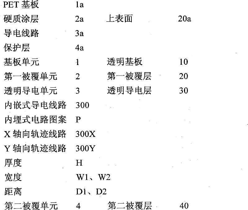
请参阅图1所示,公知技术揭露一种应用于触控面板的透明导电结构,其包括:一PET基板1a、一成形于PET基板1a的上表面上的硬质涂层2a、多个成形于PET基板1a的下表面上的导电线路3a、及一覆盖上述多个导电线路3a以保护上述多个导电线路3a的保护层4a。然而,由于上述多个导电线路3a距离硬质涂层2a的上表面20a(此为使用者用于操作触控面板所需接触的表面)仍然过大的原因,所以上述多个导电线路3a必须使用导电度(导电范围)小于0.3欧姆/平方(Ω/□)(欧姆/平方米(Ω/m2))的超低导电材料来达到感应的要求。Please refer to FIG. 1, the known technology discloses a transparent conductive structure applied to touch panels, which includes: a PET substrate 1a, a
发明内容 Contents of the invention
本发明的目的在于提供一种透明导电结构及其制作方法,其可应用于触控面板,且不需如现有技术那样使用超低导电材料来制作导电线路。The object of the present invention is to provide a transparent conductive structure and a manufacturing method thereof, which can be applied to a touch panel, and do not need to use ultra-low conductive materials to make conductive lines as in the prior art.
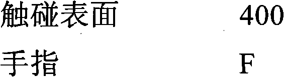
本发明实施例提供一种应用于触控面板的透明导电结构,其包括:一基板单元、一第一被覆单元、一透明导电单元及一第二被覆单元。其中,基板单元具有至少一透明基板。第一被覆单元具有至少一成形于上述至少一透明基板的上表面的第一被覆层。透明导电单元具有至少一成形于上述至少一第一被覆层的上表面的透明导电层,其中上述至少一透明导电层的内部具有多个内嵌式导电线路,且上述多个内嵌式导电线路被布局排列以形成一特定的内埋式电路图案。第二被覆单元具有至少一成形于上述至少一透明导电层的上表面且覆盖上述多个内嵌式导电线路的第二被覆层,其中上述至少一第二被覆层的顶端具有一用于提供外物(例如使用者的手指或任何的触控笔等等)触碰的触碰表面。An embodiment of the present invention provides a transparent conductive structure applied to a touch panel, which includes: a substrate unit, a first covering unit, a transparent conducting unit and a second covering unit. Wherein, the substrate unit has at least one transparent substrate. The first covering unit has at least one first covering layer formed on the upper surface of the at least one transparent substrate. The transparent conductive unit has at least one transparent conductive layer formed on the upper surface of the at least one first covering layer, wherein the inside of the at least one transparent conductive layer has a plurality of embedded conductive circuits, and the plurality of embedded conductive circuits are laid out and arranged to form a specific embedded circuit pattern. The second covering unit has at least one second covering layer formed on the upper surface of the at least one transparent conductive layer and covering the plurality of embedded conductive circuits, wherein the top of the at least one second covering layer has a A touch surface that is touched by an object (such as a user's finger or any stylus, etc.).
本发明实施例提供一种应用于触控面板的透明导电结构的制作方法,其包括:首先,提供一基板单元,其具有至少一透明基板;接着,于上述至少一透明基板的上表面成形至少一第一被覆层;然后,于上述至少一第一被覆层的上表面成形至少一内部具有多个内嵌式导电线路的透明导电层,其中上述多个内嵌式导电线路被布局排列以形成一特定的内埋式电路图案;最后,于上述至少一透明导电层的上表面成形至少一第二被覆层,以覆盖上述多个内嵌式导电线路,其中上述至少一第二被覆层的顶端具有一用于提供外物触碰的触碰表面。An embodiment of the present invention provides a method for manufacturing a transparent conductive structure applied to a touch panel, which includes: first, providing a substrate unit having at least one transparent substrate; then, forming at least one transparent substrate on the upper surface of the at least one transparent substrate A first coating layer; then, forming at least one transparent conductive layer with a plurality of embedded conductive circuits on the upper surface of the at least one first coated layer, wherein the plurality of embedded conductive circuits are laid out and arranged to form A specific embedded circuit pattern; finally, at least one second coating layer is formed on the upper surface of the at least one transparent conductive layer to cover the plurality of embedded conductive circuits, wherein the top of the at least one second coating layer There is a touch surface for providing foreign object touch.
综上所述,本发明实施例所提供的透明导电结构及其制作方法可通过“拉近上述用于提供外物触碰的触碰表面与上述特定的内埋式电路图案(此内埋式电路图案被内埋于透明导电层内)两者的距离”的设计,以使得本发明的透明导电结构及其制作方法可以在不需使用超低导电材料来制作上述多个内嵌式导电线路的情况下,即可得到导电范围可介于0.8至3欧姆/平方之间的内埋式电路图案来应用于触控面板。To sum up, the transparent conductive structure and its manufacturing method provided by the embodiments of the present invention can be achieved by "bringing the above-mentioned touch surface for providing contact with foreign objects closer to the above-mentioned specific embedded circuit pattern (the embedded circuit pattern) The circuit pattern is embedded in the transparent conductive layer) and the design of the "distance" between the two, so that the transparent conductive structure of the present invention and its manufacturing method can be produced without using ultra-low conductive materials to make the above-mentioned multiple embedded conductive circuits In the case of , an embedded circuit pattern with a conductivity ranging from 0.8 to 3 ohm/square can be obtained to be applied to the touch panel.
为使能更进一步了解本发明的特征及技术内容,请参阅以下有关本发明的详细说明与附图,然而附图仅提供参考与说明,并非用来对本发明加以限制。In order to further understand the features and technical content of the present invention, please refer to the following detailed description and accompanying drawings of the present invention. However, the accompanying drawings are for reference and illustration only, and are not intended to limit the present invention.
附图说明 Description of drawings
图1为公知应用于触控面板的透明导电结构的侧视剖面示意图;FIG. 1 is a schematic side-view cross-sectional view of a known transparent conductive structure applied to a touch panel;
图2为本发明应用于触控面板的透明导电结构的制作方法的流程图;2 is a flow chart of a method for manufacturing a transparent conductive structure applied to a touch panel according to the present invention;
图2A为本发明应用于触控面板的透明导电结构已经过步骤S100至S102的制作过程的侧视剖面示意图;2A is a schematic side-view cross-sectional view of the manufacturing process of the transparent conductive structure applied to the touch panel of the present invention after steps S100 to S102;
图2B为本发明应用于触控面板的透明导电结构已经过步骤S104的制作过程的侧视剖面示意图;2B is a schematic side view cross-sectional view of the transparent conductive structure applied to the touch panel of the present invention after step S104 of the manufacturing process;
图2C为本发明应用于触控面板的透明导电结构已经过步骤S106的制作过程的侧视剖面示意图;以及FIG. 2C is a schematic side-view cross-sectional view of the transparent conductive structure applied to the touch panel of the present invention after step S106 of the manufacturing process; and
图3为本发明多个内嵌式导电线路的布局方式的俯视示意图。FIG. 3 is a schematic top view of the layout of multiple embedded conductive circuits according to the present invention.
其中,附图标记说明如下:Wherein, the reference signs are explained as follows:
具体实施方式 Detailed ways
请参阅图2、图2A至图2C、及图3所示,其中图2为本发明制作方法的流程图,图2A至图2C分别为本发明制作方法的制作流程剖面示意图,而图3为多个内嵌式导电线路的布局方式的上视示意图。由上述图中可知,本发明提供一种应用于触控面板的透明导电结构的制作方法,其至少包括下列几个步骤(如图2中,从步骤S100至步骤S 106所示):Please refer to Fig. 2, Fig. 2A to Fig. 2C, and Fig. 3, wherein Fig. 2 is a flow chart of the production method of the present invention, Fig. 2A to Fig. 2C are respectively a schematic sectional view of the production process of the production method of the present invention, and Fig. 3 is A schematic top view of the layout of multiple embedded conductive lines. As can be seen from the above figures, the present invention provides a method for manufacturing a transparent conductive structure applied to a touch panel, which at least includes the following steps (shown from step S100 to step S106 in FIG. 2 ):
步骤S100为:首先,请配合图2与图2A所示,提供一基板单元1,其具有至少一透明基板10。举例来说,上述至少一透明基板10可为聚乙烯对苯二甲酸酯(polyethylene Terephthalate,PET)、聚碳酸酯(Poly Carbonate,PC)、聚乙烯(polyethylene,PE)、聚氯乙烯(Poly Vinyl Chloride,PVC)、聚丙烯(PolyPropylene,PP)、聚苯乙烯(Poly Styrene,PS)、或聚甲基丙烯酸甲酯(Polymethylmethacrylate,PMMA)中的其中之一,且上述至少一透明基板10的厚度大致上可介于50μm至125μm之间。换言之,设计者可依据不同的设计需求,采用不同的材料来制作上述至少一透明基板10。然而,上述所列出有关制成透明基板10的材料只是用来举例而已,其并非用以限定本发明,举凡任何可制成透明基板10的材料(例如塑料、玻璃等)皆可应用于本发明中。Step S100 is as follows: Firstly, according to FIG. 2 and FIG. 2A , a
步骤S102为:请配合图2与图2A所示,成形至少一第一被覆层20于上述至少一透明基板10的上表面。举例来说,上述至少一第一被覆层20可为一由硬质材料所制成的硬质被覆层。换言之,依据不同的设计需求,设计者可采用不同的硬质材料来制作上述至少一第一被覆层20,例如设计者所使用的硬质材料为紫外光硬化材料时,此硬质被覆层可为一紫外光硬化被覆层。然而,上述所列出有关制成第一被覆层20的材料只是用来举例而已,其并非用以限定本发明,任何可制成第一被覆层20的材料皆可应用于本发明中。Step S102 is: please cooperate with FIG. 2 and FIG. 2A to form at least one first covering
步骤S104为:请配合图2与图2B所示,于上述至少一第一被覆层20的上表面成形至少一内部具有多个内嵌式导电线路300的透明导电层30,其中上述多个内嵌式导电线路300被布局排列以形成一特定的内埋式电路图案P。举例来说,透明导电单元3可为一氧化铟锡(ITO)导电层,且上述多个内嵌式导电线路300可选择性地贯穿(如图2B所示)或不贯穿上述至少一透明导电层30。依据不同的设计需求,每一个内嵌式导电线路300可为一由银材料所制成的银线路、一由铝材料所制成的铝线路、一由铜材料所制成的铜线路、或由任何导电材料所制成的任何导电线路。每一个内嵌式导电线路300的上表面外露且可与上述至少一透明导电层30的上表面齐平。上述多个内嵌式导电线路300在不需使用超低导电材料来制作的情况下,即可使得上述特定的内埋式电路图案P的导电范围(导电度)大致上可介于0.8至3欧姆/平方(欧姆/平方米(Ω/m2))之间。换言之,设计者可依据所特定规划的内埋式电路图案P及所需要导电范围,以将多个内嵌式导电线路300内埋于上述至少一透明导电层30内(例如通过滚压上述多个内嵌式导电线路300的方式来内埋于上述至少一透明导电层30内)。Step S104 is: please cooperate with FIG. 2 and FIG. 2B to form at least one transparent
再者,请配合图2B与图3所示,上述多个内嵌式导电线路300可分成多个往横向延伸的X轴向轨迹线路300X与多个往纵向(此纵向与上述的横向大致上相互垂直)延伸且分别与上述多个X轴向轨迹线路300X相互绝缘且大致上相互垂直的Y轴向轨迹线路300Y,每一个内嵌式导电线路300的厚度H(如图2B所示)可介于


步骤S106为:请配合图2与图2C所示,于上述至少一透明导电层30的上表面成形至少一第二被覆层40,以覆盖上述多个内嵌式导电线路300,其中上述至少一第二被覆层40的顶端具有一用于提供外物(例如使用者的手指F或任何的触控笔等等)触碰的触碰表面400。举例来说,上述至少一第二被覆层40可为一由硬质材料所制成的硬质保护层,硬质保护层可为一厚度介于3μm至5μm之间的氧化物保护层,且氧化物保护层可为一由氧化硅材料所制成的氧化硅层(例如由二氧化硅(SiO2)所制成的二氧化硅层)或一由氧化铝材料所制成的氧化铝层(例如由三氧化二铝(Al2O3)所制成的三氧化二铝层)。Step S106 is: please cooperate with FIG. 2 and FIG. 2C to form at least one second coating layer 40 on the upper surface of the above-mentioned at least one transparent
请再参考图2C与图3所示,经过上述步骤S100至S106的制作过程,本发明可提供一种应用于触控面板的透明导电结构,其包括:一基板单元1、一第一被覆单元2、一透明导电单元3及一第二被覆单元4。其中,基板单元1具有至少一透明基板10。第一被覆单元2具有至少一成形于上述至少一透明基板10的上表面的第一被覆层20。透明导电单元3具有至少一成形于上述至少一第一被覆层20的上表面的透明导电层30,其中上述至少一透明导电层30的内部具有多个内嵌式导电线路300,且上述多个内嵌式导电线路300被布局排列以形成一特定的内埋式电路图案P。第二被覆单元4具有至少一成形于上述至少一透明导电层30的上表面且覆盖上述多个内嵌式导电线路300的第二被覆层40,其中上述至少一第二被覆层40的顶端具有一用于提供外物(例如使用者的手指F或任何的触控笔等等)触碰的触碰表面400。Please refer to FIG. 2C and FIG. 3 again. After the manufacturing process of the above steps S100 to S106, the present invention can provide a transparent conductive structure applied to a touch panel, which includes: a
举例来说,上述至少一透明基板10可为聚乙烯对苯二甲酸酯、聚碳酸酯、聚乙烯、聚氯乙烯、聚丙烯、聚苯乙烯、或聚甲基丙烯酸甲酯之中的其中之一,且上述至少一透明基板10的厚度可介于50μm至125μm之间。上述至少一第一被覆层20可为一硬质被覆层,且该硬质被覆层可为一紫外光硬化被覆层。每一个内嵌式导电线路300可为一银线路、一铝线路、一铜线路或任何的内嵌式导电线路,每一个内嵌式导电线路300的上表面与上述至少一透明导电层30的上表面齐平,且上述特定的内埋式电路图案P的导电范围可介于0.8至3欧姆/平方之间。For example, the above-mentioned at least one
再者,上述多个内嵌式导电线路300(如图3所示)可分成多个往横向延伸的X轴向轨迹线路300X与多个往纵向延伸且分别与上述多个X轴向轨迹线路300X相互绝缘且相互垂直的Y轴向轨迹线路300Y,每一个内嵌式导电线路300的厚度H可介于


综上所述,本发明实施例所提供的透明导电结构及其制作方法可通过“拉近上述用于提供外物触碰的触碰表面与上述特定的内埋式电路图案(此内埋式电路图案被内埋于透明导电层内)两者的距离”的设计,以使得本发明的透明导电结构及其制作方法可以在不需使用超低导电材料来制作上述多个内嵌式导电线路的情况下,即可得到导电范围可介于0.8至3欧姆/平方之间的内埋式电路图案来应用于触控面板。To sum up, the transparent conductive structure and its manufacturing method provided by the embodiments of the present invention can be achieved by "bringing the above-mentioned touch surface for providing contact with foreign objects closer to the above-mentioned specific embedded circuit pattern (the embedded circuit pattern) The circuit pattern is embedded in the transparent conductive layer) and the design of the "distance" between the two, so that the transparent conductive structure of the present invention and its manufacturing method can be produced without using ultra-low conductive materials to make the above-mentioned multiple embedded conductive circuits In the case of , an embedded circuit pattern with a conductivity ranging from 0.8 to 3 ohm/square can be obtained to be applied to the touch panel.
然而以上所述仅为本发明的实施例,不能以的限制本发明范围。即凡依本发明申请专利范围所做的均等变化及修饰,仍将不失本发明的要义所在,亦不脱离本发明的精神和范围,故都应视为本发明的进一步实施状况。However, the above descriptions are only examples of the present invention, and should not limit the scope of the present invention. That is, all equivalent changes and modifications made according to the patent scope of the present invention will still not lose the gist of the present invention, nor depart from the spirit and scope of the present invention, so all should be regarded as further implementation status of the present invention.
Claims (12)


Priority Applications (1)
| Application Number | Priority Date | Filing Date | Title |
|---|---|---|---|
| CN2011100624660A CN102682874A (en) | 2011-03-16 | 2011-03-16 | Transparent conductive structure applied to touch panel and manufacturing method thereof |
Applications Claiming Priority (1)
| Application Number | Priority Date | Filing Date | Title |
|---|---|---|---|
| CN2011100624660A CN102682874A (en) | 2011-03-16 | 2011-03-16 | Transparent conductive structure applied to touch panel and manufacturing method thereof |
Publications (1)
| Publication Number | Publication Date |
|---|---|
| CN102682874A true CN102682874A (en) | 2012-09-19 |
Family
ID=46814651
Family Applications (1)
| Application Number | Title | Priority Date | Filing Date |
|---|---|---|---|
| CN2011100624660A Pending CN102682874A (en) | 2011-03-16 | 2011-03-16 | Transparent conductive structure applied to touch panel and manufacturing method thereof |
Country Status (1)
| Country | Link |
|---|---|
| CN (1) | CN102682874A (en) |
Citations (7)
| Publication number | Priority date | Publication date | Assignee | Title |
|---|---|---|---|---|
| CN1565036A (en) * | 2001-10-05 | 2005-01-12 | 普利司通股份有限公司 | Transparent electroconductive film, method for manufacture thereof, and touch panel |
| CN1867882A (en) * | 2003-10-15 | 2006-11-22 | 3M创新有限公司 | Patterned conductor touch screen having improved optics |
| CN101578667A (en) * | 2007-01-16 | 2009-11-11 | 帝人株式会社 | Transparent conductive multilayer body and touch panel made of the same |
| CN101727223A (en) * | 2008-10-14 | 2010-06-09 | 介面光电股份有限公司 | Double-sided composite touch panel structure |
| CN101751190A (en) * | 2008-12-11 | 2010-06-23 | 时纬科技股份有限公司 | Capacitive touch panel and manufacturing method thereof |
| CN201576266U (en) * | 2009-11-27 | 2010-09-08 | 介面光电股份有限公司 | Circuit structure of transparent conductive plate and touch panel |
| US20100328248A1 (en) * | 2009-06-24 | 2010-12-30 | Ocular Lcd Inc. | Capacitive touch screen with reduced electrode trace resistance |
-
2011
- 2011-03-16 CN CN2011100624660A patent/CN102682874A/en active Pending
Patent Citations (7)
| Publication number | Priority date | Publication date | Assignee | Title |
|---|---|---|---|---|
| CN1565036A (en) * | 2001-10-05 | 2005-01-12 | 普利司通股份有限公司 | Transparent electroconductive film, method for manufacture thereof, and touch panel |
| CN1867882A (en) * | 2003-10-15 | 2006-11-22 | 3M创新有限公司 | Patterned conductor touch screen having improved optics |
| CN101578667A (en) * | 2007-01-16 | 2009-11-11 | 帝人株式会社 | Transparent conductive multilayer body and touch panel made of the same |
| CN101727223A (en) * | 2008-10-14 | 2010-06-09 | 介面光电股份有限公司 | Double-sided composite touch panel structure |
| CN101751190A (en) * | 2008-12-11 | 2010-06-23 | 时纬科技股份有限公司 | Capacitive touch panel and manufacturing method thereof |
| US20100328248A1 (en) * | 2009-06-24 | 2010-12-30 | Ocular Lcd Inc. | Capacitive touch screen with reduced electrode trace resistance |
| CN201576266U (en) * | 2009-11-27 | 2010-09-08 | 介面光电股份有限公司 | Circuit structure of transparent conductive plate and touch panel |
Similar Documents
| Publication | Publication Date | Title |
|---|---|---|
| CN203299774U (en) | Touch panel and touch display panel | |
| CN103970334A (en) | Touch panel, manufacturing method thereof and touch display panel | |
| CN101587391B (en) | How to make touch circuit diagram | |
| TW201314539A (en) | Structure of touch panel and its manufacturing method | |
| US20120273262A1 (en) | Transparent conductive structure applied to a touch panel and method of making the same | |
| TWI559201B (en) | Capacitive touch sensor panel | |
| KR20140057047A (en) | Touch screen panel and portable electronic apparatus having the same | |
| US8629944B2 (en) | Transparent conductive structure applied to a touch panel and method of making the same | |
| CN103809800A (en) | Touch panels and electronic devices | |
| CN105874410B (en) | Touch window and display device including the touch window | |
| CN101178630A (en) | Touch panel assembly and manufacturing method thereof | |
| US20120273257A1 (en) | Transparent conductive structure applied to a touch panel and method of making the same | |
| JP2012247852A (en) | Transparent conductive structure applicable to touch panel, and manufacturing method for the structure | |
| CN102682875A (en) | Transparent conductive structure applied to touch panel and manufacturing method thereof | |
| TWI462001B (en) | Single lamellar projective capacitive touch panel structure and method of manufacturing the same | |
| CN103576971B (en) | Electronic device, touch cover plate and manufacturing method thereof | |
| CN202838276U (en) | Monolithic Projected Capacitive Touch Panel Structure | |
| CN103513831A (en) | Monolithic projected capacitive touch panel structure and manufacturing method thereof | |
| US20120273256A1 (en) | Transparent conductive structure applied to a touch panel and method of making the same | |
| KR20120113507A (en) | Transparent conductive structure applied to touch panel and method of making the same | |
| CN102682874A (en) | Transparent conductive structure applied to touch panel and manufacturing method thereof | |
| US20120279758A1 (en) | Transparent conductive structure applied to a touch panel and method of making the same | |
| CN102681707A (en) | Transparent conductive structure applied to touch panel and manufacturing method thereof | |
| JP2012243280A (en) | Transparent conductive structure applicable to touch panel, and manufacturing method for the structure | |
| TWI480999B (en) | Compound induction electrode structure applied to a touch panel |
Legal Events
| Date | Code | Title | Description |
|---|---|---|---|
| C06 | Publication | ||
| PB01 | Publication | ||
| C10 | Entry into substantive examination | ||
| SE01 | Entry into force of request for substantive examination | ||
| C02 | Deemed withdrawal of patent application after publication (patent law 2001) | ||
| WD01 | Invention patent application deemed withdrawn after publication |
Application publication date: 20120919 |