CN102386464A - Double-frequency band elimination filter - Google Patents
Double-frequency band elimination filter Download PDFInfo
- Publication number
- CN102386464A CN102386464A CN201110343494XA CN201110343494A CN102386464A CN 102386464 A CN102386464 A CN 102386464A CN 201110343494X A CN201110343494X A CN 201110343494XA CN 201110343494 A CN201110343494 A CN 201110343494A CN 102386464 A CN102386464 A CN 102386464A
- Authority
- CN
- China
- Prior art keywords
- microstrip line
- microstrip
- line
- width
- length
- Prior art date
- Legal status (The legal status is an assumption and is not a legal conclusion. Google has not performed a legal analysis and makes no representation as to the accuracy of the status listed.)
- Granted
Links
Images


Landscapes
- Control Of Motors That Do Not Use Commutators (AREA)
Abstract
本发明公开一种双频带阻滤波器。该双频带阻滤波器由上层的微带结构,中间层介质基板和下层的接地金属组成。上层微带结构由三个结构相同的具有双频带阻特性的模块单元级联组成;每个模块单元由一根主传输线和半波长谐振器耦合组成;该半波长谐振器由一根微带线和中间加载的微带线组成;该半波长谐振器具有固定的奇模谐振频率和可灵活控制的偶模谐振频率;三个模块单元通过两根四分之一波长微带传输线依次相连,形成n字形结构;三个半波长谐振器位于n字形结构的内部;本发明具有良好的带阻特性,可用于无线通信的射频前端电路。

The invention discloses a dual-frequency band rejection filter. The dual-band rejection filter is composed of an upper-layer microstrip structure, a middle-layer dielectric substrate and a lower-layer ground metal. The upper microstrip structure is composed of three modular units with the same structure and dual-band rejection characteristics cascaded; each module unit is composed of a main transmission line and a half-wavelength resonator coupling; the half-wavelength resonator is composed of a microstrip line It consists of a microstrip line loaded in the middle; the half-wavelength resonator has a fixed odd-mode resonant frequency and a flexibly controllable even-mode resonant frequency; the three module units are connected in turn through two quarter-wavelength microstrip transmission lines to form N-shaped structure; three half-wavelength resonators are located inside the n-shaped structure; the invention has good band-rejection characteristics and can be used for radio frequency front-end circuits of wireless communication.
Description
技术领域 technical field
本发明涉及一种双频带阻滤波器,具体涉及一种可应用在多频带和可重构射频前端系统中的具有双频带和良好的频率选择性的带阻滤波器。 The invention relates to a dual-frequency band rejection filter, in particular to a band rejection filter with dual frequency bands and good frequency selectivity, which can be applied in multi-band and reconfigurable radio frequency front-end systems.
背景技术 Background technique
近几年来,双频甚至多频无线系统成为热点,研究人员对其进行大力开发。但这些系统有时候可能会受到寄生响应和互调失真或谐波而造成多种干扰问题。为了克服这些问题,带阻滤波器是抑制位于宽通带内不必要的窄带信号的最佳选择,也是解决这些问题的最优办法。双频带阻滤波器BSFs可以生成两个阻带频段,并保持它们之间的通带,可应用于抑制高功率放大器或混频器中不需要的双边频谱。双频带阻滤波器在许多应用中具有很多优势,与带通相滤波器相比,双频带阻滤波器有更低的插入损耗,更平滑的群延时效果。此外,双波段带阻滤波器具有比传统简单级联的两个带阻滤波器更小的尺寸以及传输损耗。 In recent years, dual-band or even multi-band wireless systems have become a hot spot, and researchers have vigorously developed them. But these systems can sometimes suffer from various interference problems caused by spurious responses and intermodulation distortion or harmonics. In order to overcome these problems, the band-stop filter is the best choice to suppress unnecessary narrow-band signals located in the wide passband, and it is also the best way to solve these problems. Dual-band stop filters BSFs can generate two stop-band frequency bands and maintain a passband between them, which can be applied to suppress unwanted side-side spectrum in high-power amplifiers or mixers. Dual-band rejection filters have many advantages in many applications. Compared with band-pass phase filters, dual-band rejection filters have lower insertion loss and smoother group delay effects. In addition, the dual band rejection filter has a smaller size and transmission loss than the traditional simple cascaded two rejection filters.
双频带阻滤波器当前已得到了广泛的研究,目前已提出了许多不同的设计方法:(1)在低通原型滤波器的基础上应用频率变换产生阻带特性。(2)是使用复合左/右手材料传输线代替传统的微带传输线,以此来产生双阻带特性。(3)是使用两阶或三阶的阶梯阻抗谐振器来设计双频带阻滤波器。(4)是分别在顶层使用分裂环谐振环和在底层使用互补分裂环谐振环产生两个阻带。(5)是使用特性阻抗可控的两条传输线依据相位差的不同实现双频带阻滤波器。(6)是同时使用包括嵌线,马刺线和常规微带线三种平面结构获得双阻带响应。 Dual-frequency band-stop filters have been extensively studied at present, and many different design methods have been proposed: (1) Applying frequency transformation on the basis of low-pass prototype filters to generate stop-band characteristics. (2) It is to use the composite left/right hand material transmission line instead of the traditional microstrip transmission line to generate double stopband characteristics. (3) is to use two-order or three-order stepped impedance resonators to design dual-band rejection filters. (4) is to use the split-ring resonant ring on the top layer and the complementary split-ring resonant ring on the bottom layer to generate two stopbands respectively. (5) Two transmission lines with controllable characteristic impedance are used to realize a dual-frequency band-stop filter according to the difference in phase difference. (6) Three planar structures including ruled line, spur line and conventional microstrip line are used at the same time to obtain a double stop band response.
发明内容 Contents of the invention
本发明的目的是利用中间加载谐振器的谐振特性实现一种平面双频带阻滤波器。本发明的双频带阻滤波器阻带频率可以很容易地实现到所需的值,结构简单,而且具有滚降特性。 The purpose of the present invention is to realize a planar double-band rejection filter by using the resonance characteristics of the intermediate loading resonator. The frequency of the double-band rejection filter of the present invention can be easily realized to the required value, has simple structure and has roll-off characteristics.
实现本发明的具体技术方案是: Realize the concrete technical scheme of the present invention is:
一种双频带阻滤波器,包括上层的微带结构、中间层介质基板和下层的接地金属;上层微带结构附着在中间层介质板上表面,中间层介质板下表面为接地金属;上层微带结构包括输入端口、输出端口、三个结构相同的具有双频带阻特性的模块单元、两个结构相同的阻抗变换器;输入端、第一模块单元、第一阻抗变换器、第二模块单元、第二阻抗变换器、第三模块单元、输出端依次相连接,整个上层微带结构形成n字型结构。 A dual-band rejection filter, comprising an upper microstrip structure, an intermediate dielectric substrate, and a lower grounded metal; the upper microstrip structure is attached to the upper surface of the intermediate dielectric board, and the lower surface of the intermediate dielectric board is grounded metal; The band structure includes an input port, an output port, three modular units with dual-frequency band-stop characteristics with the same structure, and two impedance converters with the same structure; the input terminal, the first modular unit, the first impedance converter, and the second modular unit , the second impedance converter, the third module unit, and the output end are connected in sequence, and the entire upper-layer microstrip structure forms an n-shaped structure.
作为上述双频带阻滤波器的优化技术方案,所述模块单元由第一传输线和第一半波长谐振器耦合组成;第一半波长谐振器由第一微带线、第二微带线、第三微带线、第四微带线和加载到第二微带线和第三微带线相接处的第五微带线组成;第一半波长谐振器的第二微带线和第三微带线与第一传输线组成平行耦合结构;所述第一微带线和第二微带线的长度加和等于第三微带线和第四微带线的长度加和;所述第一阻抗变换器由第六微带线和第七微带线相连接组成;第二阻抗变换器由第八微带线和第九微带线相连接组成;输入端由第十微带线构成;输出端由第十一微带线构成;输入端和输出端的传输线的特性阻抗都为50Ω。 As an optimized technical solution for the above-mentioned dual-band rejection filter, the module unit is composed of a first transmission line coupled with a first half-wavelength resonator; the first half-wavelength resonator is composed of a first microstrip line, a second microstrip line, a first half-wavelength resonator Three microstrip lines, the fourth microstrip line and the fifth microstrip line loaded to the joint of the second microstrip line and the third microstrip line; the second microstrip line and the third microstrip line of the first half-wavelength resonator The microstrip line and the first transmission line form a parallel coupling structure; the sum of the lengths of the first microstrip line and the second microstrip line is equal to the sum of the lengths of the third microstrip line and the fourth microstrip line; the first The impedance converter is formed by connecting the sixth microstrip line and the seventh microstrip line; the second impedance converter is formed by connecting the eighth microstrip line and the ninth microstrip line; the input end is formed by the tenth microstrip line; The output end is formed by the eleventh microstrip line; the characteristic impedance of the transmission line at the input end and the output end is both 50Ω.
作为上述双频带阻滤波器的优化技术方案,所述三个结构相同的模块单元所包含的三个半波长谐振器排布在上述n字型结构的内部;第一半波长谐振器和第一传输线组成平行耦合结构;第二半波长谐振器和第二传输线组成平行耦合结构;第三半波长谐振器和第三传输线组成平行耦合结构。 As an optimized technical solution for the above-mentioned dual-band rejection filter, the three half-wavelength resonators included in the three modular units with the same structure are arranged inside the above-mentioned n-shaped structure; the first half-wavelength resonator and the first half-wavelength resonator The transmission line forms a parallel coupling structure; the second half-wavelength resonator and the second transmission line form a parallel coupling structure; the third half-wavelength resonator and the third transmission line form a parallel coupling structure.
上述双频带阻滤波器,采用所述中间加载半波长谐振器实现的双频带阻滤波器,由于中间加载谐振器具有偶模谐振频率改变时奇模谐振频率固定不变的特性,可以方便的进行频率控制和设计,且具有良好的滚降特性和频率选择性。 The above-mentioned dual-frequency band-rejection filter adopts the dual-frequency band-rejection filter realized by the intermediate-loaded half-wavelength resonator, since the intermediate-loaded resonator has the characteristic that the odd-mode resonant frequency is fixed when the even-mode resonant frequency changes, it can be easily carried out. Frequency control and design with good roll-off characteristics and frequency selectivity.
作为上述双频带阻滤波器的优化技术方案,所述双频带阻滤波器的第一微带线长度为4.4mm,宽度为0.8mm;第二微带线长度为15.1mm,宽度为0.8mm;第三微带线长度为8.6mm,宽度为0.8mm;第四微带线长度为10.3mm,宽度为0.8mm;第五微带线长度为9.7mm,宽度为0.8mm;第六微带线长度为16.1mm,宽度为1.75mm;第七微带线长度为4.95mm,宽度为1.75mm;第十微带线宽度为1.85mm;第十一微带线宽度为1.85mm;第一传输线的长度为24.5mm,宽度为1.75mm;第一传输线和第一半波长谐振器之间的耦合距离为0.17mm。 As an optimized technical solution for the above-mentioned dual-band rejection filter, the length of the first microstrip line of the dual-band rejection filter is 4.4mm, and the width is 0.8mm; the length of the second microstrip line is 15.1mm, and the width is 0.8mm; The length of the third microstrip line is 8.6mm and the width is 0.8mm; the length of the fourth microstrip line is 10.3mm and the width is 0.8mm; the length of the fifth microstrip line is 9.7mm and the width is 0.8mm; the sixth microstrip line The length is 16.1mm and the width is 1.75mm; the length of the seventh microstrip line is 4.95mm and the width is 1.75mm; the width of the tenth microstrip line is 1.85mm; the width of the eleventh microstrip line is 1.85mm; the width of the first transmission line The length is 24.5mm, and the width is 1.75mm; the coupling distance between the first transmission line and the first half-wavelength resonator is 0.17mm.
本发明相对现有技术具有如下特点: The present invention has the following characteristics relative to the prior art:
(1)使用中间开路加载谐振器,通过改变中间开路加载的长度可灵活控制偶模谐振频率,而奇模谐振频率保持不变,使所需阻带频率易于控制。 (1) Using the intermediate open-circuit loaded resonator, the even-mode resonant frequency can be flexibly controlled by changing the length of the intermediate open-circuit loaded, while the odd-mode resonant frequency remains unchanged, making the required stopband frequency easy to control.
(2)本滤波器所采用耦合结构通过优化耦合区间长度使得在两个阻带频率上具有较好的滚降特性和频率选择性。 (2) The coupling structure adopted by this filter has better roll-off characteristics and frequency selectivity at the two stopband frequencies by optimizing the length of the coupling interval.
(3)本滤波器使用3级级联的形式,回波损耗在0-5GHz内超过15dB,抑制水平超过30dB。 (3) This filter adopts 3-stage cascaded form, the return loss exceeds 15dB within 0-5GHz, and the suppression level exceeds 30dB.
附图说明 Description of drawings
图1为本发明的双频带阻滤波器的结构示意图。 FIG. 1 is a schematic structural diagram of a dual-band rejection filter of the present invention.
图2为本发明的双频带阻滤波器的模块单元。 Fig. 2 is the module unit of the dual-band rejection filter of the present invention.
图3a为中间开路加载谐振器的结构示意图。 Fig. 3a is a schematic diagram of the structure of a middle open-circuit loaded resonator.
图3b为中间开路加载谐振器的奇模激励等效结构图。 Fig. 3b is an equivalent structural diagram of an odd-mode excitation of a middle open-circuit loaded resonator.
图3c为中间开路加载谐振器的偶模激励等效结构图。 Fig. 3c is an equivalent structure diagram of an even-mode excitation of a middle open-circuit loaded resonator.
图4为中间开路加载的长度L5取不同值时的对比图。 Fig. 4 is a comparison diagram when the length L 5 of the middle open-circuit load takes different values.
图5为双频带阻滤波器的仿真与测量曲线。 Figure 5 shows the simulation and measurement curves of the dual-band rejection filter.
具体实施方式 Detailed ways
下面结合附图对本发明的实施做详细说明,但本发明要求的保护范围不限于下述的实施方式。 The implementation of the present invention will be described in detail below in conjunction with the accompanying drawings, but the scope of protection required by the present invention is not limited to the following embodiments.
如图1所示,双频带阻滤波器包括上层的微带结构,中间层介质基板和下层的接地金属;上层微带结构附着在中间层介质板上表面,中间层介质板下表面为接地金属;上层微带结构包括输入端口、输出端口、三个结构相同的具有双频带阻特性的模块单元、两个结构相同的阻抗变换器;输入端、第一模块单元、第一阻抗变换器、第二模块单元、第二阻抗变换器、第三模块单元、输出端依次相连接,整个上层微带结构形成n字型结构。 As shown in Figure 1, the dual-band rejection filter includes an upper microstrip structure, an intermediate dielectric substrate and a lower grounded metal; the upper microstrip structure is attached to the upper surface of the intermediate dielectric board, and the lower surface of the intermediate dielectric board is grounded metal ; The upper layer microstrip structure includes an input port, an output port, three module units with the same structure and dual-frequency band-rejection characteristics, and two impedance converters with the same structure; the input terminal, the first module unit, the first impedance converter, the second The second module unit, the second impedance converter, the third module unit, and the output end are connected sequentially, and the entire upper-layer microstrip structure forms an n-shaped structure.
所述第一模块单元由第一传输线2和第一半波长谐振器15耦合组成;第一半波长谐振器15由第一微带线10、第二微带线11、第三微带线13、第四微带线14和加载到第二微带线11和第三微带线13相接处的第五微带线12组成;第一半波长谐振器15的第二微带线11和第三微带线13与第一传输线2组成平行耦合结构;所述第一微带线10和第二微带线11的长度加和等于第三微带线13和第四微带线14的长度加和;所述第一阻抗变换器由第六微带线3和第七微带线4相连接组成;第二阻抗变换器由第八微带线6和第九微带线7相连接组成;输入端由第十微带线1构成;输出端由第十一微带线9构成;输入端和输出端的传输线的特性阻抗都为50Ω。
The first module unit is composed of the coupling of the
所述三个结构相同的模块单元所包含的三个半波长谐振器排布在上述n字型结构的内部;第一半波长谐振器15和第一传输线2组成平行耦合结构;第二半波长谐振器16和第二传输线5组成平行耦合结构;第三半波长谐振器17和第三传输线8组成平行耦合结构。
The three half-wavelength resonators contained in the three modular units with the same structure are arranged inside the above-mentioned n-shaped structure; the first half-
图2是所述模块单元的结构图,模块单元具有双频带阻特性。图中内虚线框是中间开路加载谐振器。谐振器和主传输线平行耦合,当谐振器发生谐振时,主传输线的阻抗特性受到谐振器的影响,使得主传输线输入输出不匹配,信号被反射回去,从而实现带阻特性。 Fig. 2 is a structural diagram of the module unit, and the module unit has a dual-frequency band-stop characteristic. The dotted box in the figure is the open-circuit loaded resonator in the middle. The resonator and the main transmission line are coupled in parallel. When the resonator resonates, the impedance characteristics of the main transmission line are affected by the resonator, so that the input and output of the main transmission line do not match, and the signal is reflected back, thereby realizing the band stop characteristic.
图3a是所述中间开路加载谐振器。Y1、L9和Y2、L5分别是两条微带线的特征阻抗和长度。中间开路加载谐振器具有两个谐振频率,分别为偶模谐振频率和奇模谐振频率。在奇模输入 

上式中c是真空中的光速,εeff是介质的介电常数。 In the above formula, c is the speed of light in vacuum, and εeff is the dielectric constant of the medium.
在偶模输入
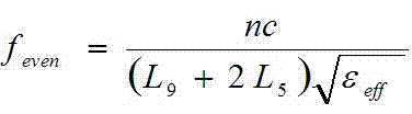
从上面两式可以看出,奇模谐振频率只与L9有关,和L5无关,而偶模谐振频率和L9和L5都相关。 It can be seen from the above two formulas that the odd-mode resonant frequency is only related to L9 and has nothing to do with L5, while the even-mode resonant frequency is related to both L9 and L5.
由此得出:所述中间开路加载谐振器具有两个谐振频率(偶模谐振频率和奇模谐振频率),而且具有当偶模谐振频率改变时奇模谐振频率固定不变的特性。本发明正是基于这条思路进行设计的。本发明中的双频阻带中的较低频率对应于谐振器的奇模谐振频率,较高频率对应于偶模谐振频率。当谐振器与主传输线之间的耦合区间调整到最优结构,即改变耦合系数在两个阻带频率上的值,使得两个阻带的抑制水平相当时,整个滤波器具有较好的性能。 It can thus be concluded that the middle open-circuit loaded resonator has two resonant frequencies (even-mode resonant frequency and odd-mode resonant frequency), and has the characteristic that the odd-mode resonant frequency is fixed when the even-mode resonant frequency changes. The present invention is designed based on this thinking just. The lower frequency in the dual-frequency stopband in the present invention corresponds to the odd-mode resonant frequency of the resonator, and the higher frequency corresponds to the even-mode resonant frequency. When the coupling interval between the resonator and the main transmission line is adjusted to the optimal structure, that is, the value of the coupling coefficient at the two stopband frequencies is changed so that the suppression levels of the two stopbands are equivalent, the entire filter has better performance .
根据上面所述,本发明双频带阻滤波器的频率易于控制,可以通过改变中间开路加载L5的长度来实现所需要的工作频率。图4所示为当L5的长度分别为8.2mm、9.2mm、9.7mm、10.2mm、10.7mm时整个滤波器的传输特性仿真,当偶模谐振频率从3.29GHz变为3.65GHz时,奇模谐振频率固定不变。 According to the above, the frequency of the dual-band rejection filter of the present invention is easy to control, and the required operating frequency can be realized by changing the length of the open-circuit load L5 in the middle. Figure 4 shows the simulation of the transmission characteristics of the entire filter when the lengths of L5 are 8.2mm, 9.2mm, 9.7mm, 10.2mm, and 10.7mm respectively. When the even-mode resonant frequency changes from 3.29GHz to 3.65GHz, the odd-mode The resonant frequency is fixed.
在下面实施例中,双频带阻滤波器制作在相对介电常数为3.38、厚度为0.81mm、损耗因子为0.0027的介质基板上。 In the following embodiments, the dual-band rejection filter is fabricated on a dielectric substrate with a relative permittivity of 3.38, a thickness of 0.81 mm, and a loss factor of 0.0027.
实施实例: 2.43GHz和3.46GHz双频带阻滤波器 Implementation example: 2.43GHz and 3.46GHz dual-band rejection filter
2.43GHz和3.46GHz双频带阻滤波器结构如图1所示。具体参数为:第一微带线10长度为4.4mm,宽度为0.8mm;第二微带线11长度为15.1mm,宽度为0.8mm;第三微带线13长度为8.6mm,宽度为0.8mm;第四微带线14长度为10.3mm,宽度为0.8mm;第五微带线12长度为9.7mm,宽度为0.8mm;第六微带线3长度为16.1mm,宽度为1.75mm;第七微带线4长度为4.95mm,宽度为1.75mm;第十微带线1宽度为1.85mm;第十一微带线9宽度为1.85mm;第一传输线2的长度为24.5mm,宽度为1.75mm;第一传输线2和第一半波长谐振器15之间的耦合距离为0.17mm。图5给出了利用上述参数所设计的滤波器进行仿真和实际测量的结果,其中仿真和实际测量分别是使用Zeland’s IE3D和E5071C网络分析仪来完成。如图5所示,滤波器的两个阻带频率为2.43GHz和3.46GHz。在两个阻带频率上抑制水平都超过30dB。在整个通带内回波损耗也大于15dB,插入损耗为0.6dB,具有良好的性能。滤波器共有4个传输零点,分别在2.37GHz、2.63GHz、3.02GHz、3.67GHz。都靠近于阻带边缘,极大改善了滤波器滚降特性。
The structure of 2.43GHz and 3.46GHz dual-band rejection filter is shown in Figure 1. The specific parameters are: the length of the
本发明基于中间开路加载谐振器的谐振频率特性设计,采用三级级联的结构,使所述滤波器具有频率易于控制,设计简便,滚降特性良好的特点。通过调节设计的参数,可以调节带宽,即这种结构可以用来实现各种带宽规格。 The present invention is based on the resonant frequency characteristic design of the open-circuit loaded resonator in the middle, and adopts a three-stage cascaded structure, so that the filter has the characteristics of easy frequency control, simple design and good roll-off characteristics. By adjusting the parameters of the design, the bandwidth can be adjusted, that is, this structure can be used to achieve various bandwidth specifications.
以上所述仅为本发明的较佳实例,并不用以限制本发明,凡在本发明的精神和原则之内,所作的任何修改、等同替换、改进等,均应包含在本发明的保护范围之内。 The above descriptions are only preferred examples of the present invention, and are not intended to limit the present invention. Any modifications, equivalent replacements, improvements, etc. made within the spirit and principles of the present invention should be included in the protection scope of the present invention within.
Claims (5)
Priority Applications (1)
| Application Number | Priority Date | Filing Date | Title |
|---|---|---|---|
| CN201110343494XA CN102386464B (en) | 2011-11-03 | 2011-11-03 | Double-frequency band elimination filter |
Applications Claiming Priority (1)
| Application Number | Priority Date | Filing Date | Title |
|---|---|---|---|
| CN201110343494XA CN102386464B (en) | 2011-11-03 | 2011-11-03 | Double-frequency band elimination filter |
Publications (2)
| Publication Number | Publication Date |
|---|---|
| CN102386464A true CN102386464A (en) | 2012-03-21 |
| CN102386464B CN102386464B (en) | 2013-11-27 |
Family
ID=45825607
Family Applications (1)
| Application Number | Title | Priority Date | Filing Date |
|---|---|---|---|
| CN201110343494XA Expired - Fee Related CN102386464B (en) | 2011-11-03 | 2011-11-03 | Double-frequency band elimination filter |
Country Status (1)
| Country | Link |
|---|---|
| CN (1) | CN102386464B (en) |
Cited By (6)
| Publication number | Priority date | Publication date | Assignee | Title |
|---|---|---|---|---|
| CN103413997A (en) * | 2013-08-01 | 2013-11-27 | 南京理工大学 | Vertical interdigital LTCC band-pass filter |
| CN110061333A (en) * | 2019-04-04 | 2019-07-26 | 电子科技大学 | A kind of microwave electricity tune bandstop filter of high degree of suppression and broad tuning range |
| CN110148817A (en) * | 2019-06-11 | 2019-08-20 | 上海海事大学 | The four transmission zero Double-frequency band elimination filters based on all-pass coupling line |
| CN110534853A (en) * | 2019-09-07 | 2019-12-03 | 西南交通大学 | A kind of multi-frequency band elimination filter based on symmetrical fissions structure multimode resonator |
| CN114499455A (en) * | 2022-01-17 | 2022-05-13 | 西南交通大学 | An all-pass adjustable delay filter circuit |
| RU2784658C1 (en) * | 2022-04-11 | 2022-11-29 | Федеральное государственное бюджетное научное учреждение "Федеральный исследовательский центр "Красноярский научный центр Сибирского отделения Российской академии наук" (ФИЦ КНЦ СО РАН, КНЦ СО РАН) | Strip frequency doubler |
Citations (2)
| Publication number | Priority date | Publication date | Assignee | Title |
|---|---|---|---|---|
| US5512539A (en) * | 1992-04-22 | 1996-04-30 | Sumitomo Electric Industries, Ltd. | Microwave component of compound oxide superconductor material having crystal orientation for reducing electromagnetic field penetration |
| CN202363564U (en) * | 2011-11-03 | 2012-08-01 | 华南理工大学 | Double-frequency band elimination filter |
-
2011
- 2011-11-03 CN CN201110343494XA patent/CN102386464B/en not_active Expired - Fee Related
Patent Citations (2)
| Publication number | Priority date | Publication date | Assignee | Title |
|---|---|---|---|---|
| US5512539A (en) * | 1992-04-22 | 1996-04-30 | Sumitomo Electric Industries, Ltd. | Microwave component of compound oxide superconductor material having crystal orientation for reducing electromagnetic field penetration |
| CN202363564U (en) * | 2011-11-03 | 2012-08-01 | 华南理工大学 | Double-frequency band elimination filter |
Cited By (9)
| Publication number | Priority date | Publication date | Assignee | Title |
|---|---|---|---|---|
| CN103413997A (en) * | 2013-08-01 | 2013-11-27 | 南京理工大学 | Vertical interdigital LTCC band-pass filter |
| CN103413997B (en) * | 2013-08-01 | 2015-11-04 | 南京理工大学 | Vertical interdigitated LTCC bandpass filter |
| CN110061333A (en) * | 2019-04-04 | 2019-07-26 | 电子科技大学 | A kind of microwave electricity tune bandstop filter of high degree of suppression and broad tuning range |
| CN110061333B (en) * | 2019-04-04 | 2021-04-06 | 电子科技大学 | Microwave electrically tunable band-stop filter with high suppression degree and wide tuning range |
| CN110148817A (en) * | 2019-06-11 | 2019-08-20 | 上海海事大学 | The four transmission zero Double-frequency band elimination filters based on all-pass coupling line |
| CN110534853A (en) * | 2019-09-07 | 2019-12-03 | 西南交通大学 | A kind of multi-frequency band elimination filter based on symmetrical fissions structure multimode resonator |
| CN114499455A (en) * | 2022-01-17 | 2022-05-13 | 西南交通大学 | An all-pass adjustable delay filter circuit |
| CN114499455B (en) * | 2022-01-17 | 2023-04-28 | 西南交通大学 | An all-pass adjustable delay filter circuit |
| RU2784658C1 (en) * | 2022-04-11 | 2022-11-29 | Федеральное государственное бюджетное научное учреждение "Федеральный исследовательский центр "Красноярский научный центр Сибирского отделения Российской академии наук" (ФИЦ КНЦ СО РАН, КНЦ СО РАН) | Strip frequency doubler |
Also Published As
| Publication number | Publication date |
|---|---|
| CN102386464B (en) | 2013-11-27 |
Similar Documents
| Publication | Publication Date | Title |
|---|---|---|
| CN102324599B (en) | Balanced type radio frequency voltage tunable bandpass filter with constant absolute bandwidth | |
| CN102832433B (en) | Non-uniform power divider with integrated band-pass filtering function | |
| CN102403562A (en) | Powder divider integrating a dual-frequency bandpass filter | |
| CN102280678B (en) | Balanced radio frequency electrically tunable bandpass filter with constant relative bandwidth | |
| CN101916892B (en) | Tunable band-stop filter of constant absolute bandwidth based on modular structure | |
| CN102832434B (en) | Equal power splitter integrating band-pass filtering function | |
| CN106571507A (en) | Multifunctional reconfigurable filter based on principle of signal interference | |
| Narayane et al. | A selective wideband bandpass filter with wide stopband using mixed lumped-distributed circuits | |
| CN102403563A (en) | Powder divider integrating single-frequency bandpass filter | |
| CN202363564U (en) | Double-frequency band elimination filter | |
| CN101699649B (en) | Plane compact type three-passband filter | |
| US7541888B2 (en) | Dual band coupled-line balanced-to-unbalanced bandpass filter | |
| CN113140882A (en) | Miniaturized filtering crossing directional coupler with wide pass band and wide stop band response | |
| CN102386464B (en) | Double-frequency band elimination filter | |
| CN110277616B (en) | Swastika-type dual-passband band-pass filter based on vertical folding miniaturization | |
| Zhu et al. | Novel tunable isolation network used in ring-type single-to-balanced, power-dividing, and single-ended filter with arbitrary power-division ratios | |
| CN103338017B (en) | A kind of 180 degree, the broadband with harmonic restraining function coupler of lumped parameter | |
| CN202308258U (en) | Power divider integrated with single-frequency band-pass filters | |
| Wong et al. | Multifolded bandwidth branch line coupler with filtering characteristic using coupled port feeding | |
| CN202737076U (en) | Equal power distributor integrated with band-pass filtering function | |
| CN111710944B (en) | Multilayer self-packaged ultra-wideband impedance transformation balun band-pass filter | |
| CN202308257U (en) | Power divider integrated with double-frequency band-pass filter | |
| CN202364184U (en) | Balanced radio frequency electric adjustment band pass filter with constant absolute bandwidth | |
| CN105789789A (en) | Tunable dual-band bandstop filter based on center loaded coupling structure | |
| You et al. | Miniature on-chip bandpass power divider with equal-ripple response and wide upper stopband |
Legal Events
| Date | Code | Title | Description |
|---|---|---|---|
| C06 | Publication | ||
| PB01 | Publication | ||
| C10 | Entry into substantive examination | ||
| SE01 | Entry into force of request for substantive examination | ||
| C14 | Grant of patent or utility model | ||
| GR01 | Patent grant | ||
| EE01 | Entry into force of recordation of patent licensing contract |
Application publication date: 20120321 Assignee: COMBA TELECOM TECHNOLOGY (GUANGZHOU) Ltd. Assignor: South China University of Technology Contract record no.: X2019440000041 Denomination of invention: Double-frequency band elimination filter Granted publication date: 20131127 License type: Exclusive License Record date: 20191202 |
|
| EE01 | Entry into force of recordation of patent licensing contract | ||
| CF01 | Termination of patent right due to non-payment of annual fee |
Granted publication date: 20131127 |
|
| CF01 | Termination of patent right due to non-payment of annual fee |