CN202364184U - Balanced radio frequency electric adjustment band pass filter with constant absolute bandwidth - Google Patents
Balanced radio frequency electric adjustment band pass filter with constant absolute bandwidth Download PDFInfo
- Publication number
- CN202364184U CN202364184U CN2011201771732U CN201120177173U CN202364184U CN 202364184 U CN202364184 U CN 202364184U CN 2011201771732 U CN2011201771732 U CN 2011201771732U CN 201120177173 U CN201120177173 U CN 201120177173U CN 202364184 U CN202364184 U CN 202364184U
- Authority
- CN
- China
- Prior art keywords
- microstrip line
- wave resonator
- input
- wavelength resonator
- radio frequency
- Prior art date
- Legal status (The legal status is an assumption and is not a legal conclusion. Google has not performed a legal analysis and makes no representation as to the accuracy of the status listed.)
- Expired - Lifetime
Links
Images


Landscapes
- Control Of Motors That Do Not Use Commutators (AREA)
Abstract
本实用新型公开具有恒定绝对带宽的平衡式射频电调带通滤波器。该带通滤波器由上层的的微带结构,中间层介质基板和下层的接地金属组成。上层微带结构采用平衡电路,包括四个半波长谐振器、两个输入馈电网络、两个输出馈电网络、两个输入端口和两个输出端口;四个半波长谐振器都由微带线和两端连接的变容二极管组成;第一半波长谐振器和第三半波长谐振器中间均加载电容;第二半波长谐振器和第四半波长谐振器弯折对称排布;整个滤波器结构镜像对称。本实用新型的平衡式射频电调滤波器实现中心频率调谐时带宽绝对恒定、能抑制共模干扰,可用于无线通信的可重构射频前端。

The utility model discloses a balanced radio frequency electric regulation band-pass filter with constant absolute bandwidth. The bandpass filter is composed of a microstrip structure in the upper layer, a dielectric substrate in the middle layer and a ground metal in the lower layer. The upper microstrip structure adopts a balanced circuit, including four half-wavelength resonators, two input feed networks, two output feed networks, two input ports and two output ports; the four half-wavelength resonators are composed of microstrip The first half-wavelength resonator and the third half-wavelength resonator are loaded with capacitance in the middle; the second half-wavelength resonator and the fourth half-wavelength resonator are bent and symmetrically arranged; the entire filter The device structure is mirror-symmetrical. The balanced radio frequency electronically adjustable filter of the utility model realizes absolutely constant bandwidth when the central frequency is tuned, can suppress common mode interference, and can be used as a reconfigurable radio frequency front end of wireless communication.
Description
技术领域 technical field
本实用新型涉及中心频率可调的平衡式射频电调带通滤波器,具体涉及一种可应用在多频带、宽频带和可重构射频前端系统中的具有恒定绝对带宽的平衡式射频电调带通滤波器。 The utility model relates to a balanced radio frequency electric regulation bandpass filter with adjustable center frequency, in particular to a balanced radio frequency electric regulation with constant absolute bandwidth that can be applied in multi-band, wide-band and reconfigurable radio frequency front-end systems bandpass filter. the
背景技术 Background technique
现代超宽带雷达和无线通信要求采用高性能的可重构射频前端。例如在认知无线电体系中,为了充分利用和融合各种不同的无线信道和标准,射频前端需要工作在不同的频率上,这就需要中心频率可调谐的可重构射频前端。射频电调带通滤波器是可重构射频前端的重要组成部分,因此日益受到重视。在这个方面,目前已经有一些研究报道,多种不同的调谐器件也已经被使用,例如半导体变容二极管、射频微机电系统(RF MEMS)电容管以及铁电薄膜材料变容管等。 Modern ultra-wideband radar and wireless communications require high-performance reconfigurable RF front-ends. For example, in the cognitive radio system, in order to fully utilize and integrate various wireless channels and standards, the RF front-end needs to work at different frequencies, which requires a reconfigurable RF front-end with tunable center frequency. As an important part of the reconfigurable RF front-end, RF electronically tuned band-pass filters are receiving increasing attention. In this regard, there have been some research reports, and a variety of different tuning devices have also been used, such as semiconductor varactors, radio frequency micro-electromechanical systems (RF MEMS) capacitors, and ferroelectric thin-film material varactors. the
不管采用哪种调谐器件,射频电调带通滤波器所面临的问题,主要包括: No matter which tuning device is used, the problems faced by the RF electric tuning bandpass filter mainly include:
(1)例如当调谐通带的中心频率时,通带的绝对带宽也会随之发生变化,而在很多应用中无线信道的绝对带宽是恒定不变的,因此我们需要在调谐中心频率的时候使通带的绝对带宽保持恒定不变。 (1) For example, when tuning the center frequency of the passband, the absolute bandwidth of the passband will also change accordingly, and in many applications the absolute bandwidth of the wireless channel is constant, so we need to tune the center frequency Keeps the absolute bandwidth of the passband constant.
(2)系统周围环境噪声的干扰。环境噪声的存在导致滤波器的性能下降,从而影响到射频前端的整体性能。因此必须采取一些抑制环境噪声的方法。 (2) Interference from environmental noise around the system. The presence of environmental noise leads to a decrease in the performance of the filter, thereby affecting the overall performance of the RF front-end. Therefore, some measures must be taken to suppress environmental noise. the
针对中心频率调谐时带宽恒定的问题,目前已经提出了一些方法。根据“M. Sanchez-Renedo, R. Gomez-Garcia, J. I. Alonso, and C. Briso-Rodriguez, Tunable combline filter with continuous control of center frequency and bandwidth, IEEE Trans. Microw. Theory Tech., vol. 53, no. 1, pp. 191-199, Jan, 2005.”所提供的分析可知,通过在谐振器之间插入介质来控制耦合系数,从而能够满足带宽恒定。根据“S. J. Park, and G. M. Rebeiz, Low-loss two-pole tunable filters with three different predefined bandwidth characteristics, IEEE Trans. Microw. Theory Tech., vol. 56, no. 5, pp. 1137-1148, May, 2008.”所提供的分析可知,采用独立的电耦合和磁耦合机制来控制耦合系数的变化,能够实现特定的带宽特性。根据“M. A. El-Tanani, and G. M. Rebeiz, High-Performance 1.5-2.5-GHz RF-MEMS Tunable Filters for Wireless Applications, IEEE Trans. Microw. Theory Tech., vol. 58, no. 6, pp. 1629-1637, Jun, 2010.”所提供的分析可知,采用电磁混合耦合机制同样能够满足带宽恒定。然而上面所提出的方法都是单端口电路,对于环境噪声的抑制基本无能为力。
Aiming at the problem of constant bandwidth when the center frequency is tuned, some methods have been proposed so far. According to "M. Sanchez-Renedo, R. Gomez-Garcia, J. I. Alonso, and C. Briso-Rodriguez, Tunable combline filter with continuous control of center frequency and bandwidth , IEEE Trans. Microw. Theory Tech., vol. 53,
平衡结构电路对环境噪声有较好的抑制效果,因此平衡电路在现代通信系统中得到广泛应用。当前大部分的研究主要集中在阻带扩展、共模抑制、拓宽通带或者使用差模响应获得双频带。根据“J. Shi, and Q. Xue, Balanced Bandpass Filters Using Center-Loaded Half-Wavelength Resonators, IEEE Trans. Microw. Theory Tech., vol. 58, no. 4, pp. 970-977, Apr, 2010.”所提供的分析可知,中间加载电阻的方式可以吸收共模信号。但上面所述的平衡式滤波器设计都是频率不可调的。到目前为止还没有任何研究报告是关于具有绝对带宽控制和共模抑制特性的平衡式射频电调滤波器。 Balanced structure circuits have a good suppression effect on environmental noise, so balanced circuits are widely used in modern communication systems. Most of the current research focuses on stopband extension, common-mode rejection, broadening the passband, or using differential-mode response to obtain dual-band. According to "J. Shi, and Q. Xue, Balanced Bandpass Filters Using Center-Loaded Half-Wavelength Resonators , IEEE Trans. Microw. Theory Tech., vol. 58, no. 4, pp. 970-977, Apr, 2010. "The analysis provided shows that the way of loading the resistor in the middle can absorb the common mode signal. But the above-mentioned balanced filter design is not frequency adjustable. So far there is no research report on balanced RF electrically tunable filters with absolute bandwidth control and common-mode rejection characteristics.
实用新型内容 Utility model content
为了达到恒定绝对带宽,并对环境噪声这类共模信号进行抑制,本实用新型提供了具有恒定绝对带宽的平衡式射频电调带通滤波器,该平衡式带通滤波器不仅中心频率调谐时绝对带宽恒定,而且对共模信号具有很好的抑制作用。 In order to achieve a constant absolute bandwidth and suppress common-mode signals such as environmental noise, the utility model provides a balanced radio frequency electronically adjustable band-pass filter with a constant absolute bandwidth. The balanced band-pass filter not only Constant absolute bandwidth and good rejection of common-mode signals. the
本实用新型解决其技术问题所采用的技术方案是: The technical scheme that the utility model solves its technical problem adopts is:
具有恒定绝对带宽的平衡式射频电调带通滤波器,包括上层的微带结构,中间层介质基板和下层的接地金属;上层微带结构附着在中间层介质板上表面,中间层介质板下表面为接地金属;上层微带结构包括四个半波长谐振器、两个输入馈电网络、两个输出馈电网络、两个输入端口和两个输出端口,两个输入端口分别与两个输入馈电网络连接,两个输出端口分别与两个输出馈电网络连接,两个输入馈电网络以抽头线方式分别与第一半波长谐振器相接,第一半波长谐振器再分别与第二半波长谐振器和第四半波长谐振器相接,第二半波长谐振器和第四半波长谐振器再分别与第三半波长谐振器耦合,第三半波长谐振器再以抽头线方式分别与两个输出馈电网络相接,第一半波长谐振器和第三半波长谐振器的中间均加载有用于吸收共模信号的不同大小的电容,上述所有半波长谐振器的两端均有变容二极管。 A balanced RF electronically tuned bandpass filter with constant absolute bandwidth, including the upper microstrip structure, the middle dielectric substrate and the lower ground metal; the upper microstrip structure is attached to the upper surface of the middle dielectric board, and the lower middle dielectric board The surface is grounded metal; the upper microstrip structure includes four half-wavelength resonators, two input feed networks, two output feed networks, two input ports and two output ports, and the two input ports are respectively connected to the two input The feed network is connected, the two output ports are respectively connected to the two output feed networks, the two input feed networks are respectively connected to the first half-wavelength resonator in the form of a tap line, and the first half-wavelength resonator is connected to the second half-wavelength resonator respectively. The second half-wavelength resonator is connected to the fourth half-wavelength resonator, the second half-wavelength resonator and the fourth half-wavelength resonator are respectively coupled to the third half-wavelength resonator, and the third half-wavelength resonator is then tapped. They are respectively connected to the two output feed networks. The middle of the first half-wavelength resonator and the third half-wavelength resonator are loaded with capacitors of different sizes for absorbing common mode signals. Both ends of all the above-mentioned half-wavelength resonators are There are varactor diodes.
上述的具有恒定绝对带宽的平衡式射频电调带通滤波器中,所述第一半波长谐振器由第一变容二极管、第一微带线、第二微带线、第三微带线、第四微带线和第二变容二极管顺次连接构成,第一变容二极管和第二变容二极管的阳极均穿过中间层介质基板与下层接地金属相连,第三半波长谐振器与第一半波长谐振器结构相同;第二半波长谐振器由第三变容二极管、第五微带线、第六微带线、第七微带线、第四变容二极管顺次连接构成,第三变容二极管和第四变容二极管的阳极均穿过中间层介质基板与下层接地金属相连,第四半波长谐振器与第二半波长谐振器结构相同且位于第一半波长谐振器和第三半波长谐振器之间;第二半波长谐振器的第五微带线和第一半波长谐振器的第二微带线平行设置构成级间耦合结构;第二半波长谐振器的第七微带线和第三半波长谐振器的第十微带线平行设置构成级间耦合结构;上述四个半波长谐振器排布成左右、上下均对称的结构;两个输入馈电网络中的第一输入馈电网络由第一电容、第八微带线顺次连接构成,第八微带线另一端以抽头线方式接到第一半波长谐振器的第二微带线上;第二输入馈电网络的结构与第一输入馈电网络相同;两个输入端口中的第一输入端口由第九微带线构成,第九微带线与第一输入馈电网络的第一电容始端连接,第二输入端口与第一输入端口结构相同, 两个输入馈电网络与两个输出馈电网络结构相同,两个输入端口和两个输出端口结构相同;两个输入馈电网络、两个输出馈电网络、两个输入端口、两个输出端口和上述四个半波长谐振器一起排布成左右、上下均对称的结构。 In the above-mentioned balanced radio frequency electronically adjustable bandpass filter with constant absolute bandwidth, the first half-wavelength resonator is composed of a first varactor diode, a first microstrip line, a second microstrip line, and a third microstrip line , the fourth microstrip line and the second varactor diode are connected in sequence, the anodes of the first varactor diode and the second varactor diode pass through the intermediate dielectric substrate and are connected to the lower ground metal, and the third half-wavelength resonator and The structure of the first half-wavelength resonator is the same; the second half-wavelength resonator is composed of the third varactor diode, the fifth microstrip line, the sixth microstrip line, the seventh microstrip line, and the fourth varactor diode connected in sequence, The anodes of the third varactor diode and the fourth varactor diode are both connected to the lower ground metal through the intermediate layer dielectric substrate, and the fourth half-wavelength resonator has the same structure as the second half-wavelength resonator and is located between the first half-wavelength resonator and the second half-wavelength resonator. Between the third half-wavelength resonators; the fifth microstrip line of the second half-wavelength resonator and the second microstrip line of the first half-wavelength resonator are arranged in parallel to form an interstage coupling structure; the fifth microstrip line of the second half-wavelength resonator The seven microstrip lines and the tenth microstrip line of the third half-wavelength resonator are arranged in parallel to form an interstage coupling structure; the above-mentioned four half-wavelength resonators are arranged in a symmetrical structure both left and right and up and down; in the two input feed networks The first input feed network of the first input feed network is composed of the first capacitor and the eighth microstrip line connected in sequence, and the other end of the eighth microstrip line is connected to the second microstrip line of the first half-wavelength resonator in the form of a tap line; the second microstrip line The structure of the two-input feed network is the same as that of the first input feed network; the first input port in the two input ports is composed of the ninth microstrip line, and the ninth microstrip line is connected to the first capacitor of the first input feed network. The beginning connection, the second input port has the same structure as the first input port, the two input feed networks have the same structure as the two output feed networks, the two input ports and the two output ports have the same structure; the two input feed networks, The two output feeding networks, the two input ports, the two output ports and the above four half-wavelength resonators are arranged together to form a symmetrical structure both left and right and up and down. the
上述具有恒定绝对带宽的平衡式射频电调带通滤波器中,所述电容另一端均穿过中间层介质基板与下层接地金属相连。 In the above-mentioned balanced radio frequency electronically tuned bandpass filter with constant absolute bandwidth, the other ends of the capacitors pass through the intermediate dielectric substrate and are connected to the ground metal on the lower layer. the
所述的具有恒定绝对带宽的平衡式射频电调带通滤波器,当第一输入端口和第二输入端口输入差模信号时,整个滤波器在第一半波长谐振器和第三半波长谐振器的中点所在的直线位置上形成一个电隔离墙。由于这种结构在谐振器之间的耦合主要是电耦合,第一半波长谐振器和第三半波长谐振器在中间位置没有电流,接在第一半波长谐振器和第三半波长谐振器中间加载的所述电容可以忽略,因此在差模激励下,第一半波长谐振器和第三半波长谐振器等效为两个相同的四分之一波长的谐振器,同时和第二半波长谐振器耦合形成带通滤波器结构;当第一输入端口和第二输入端口输入共模信号时,整个滤波器在第一半波长谐振器和第三半波长谐振器的中点所在的直线位置上形成一个磁隔离墙。第一半波长谐振器和第三半波长谐振器在中间位置有电流流通,接在第一半波长谐振器和第三半波长谐振器中间加载的所述电容上有电流流通。第一半波长谐振器和第三半波长谐振器等效的两个四分之一波长的谐振器需要考虑中间加载的所述电容。由于第一半波长谐振器和第三半波长谐振器上的中间加载的所述电容不一样,实际工作等效的两个四分之一波长谐振器的谐振频率不同,使得共模信号不能通过,达到抑制的效果。所述全部输入输出馈电网络采用抽头线馈电方式,能得到更好的外部品质因数;在耦合区域采用电磁混合耦合机制能够满足恒定绝对带宽。 In the balanced radio frequency electronically adjustable bandpass filter with a constant absolute bandwidth, when the first input port and the second input port input differential mode signals, the entire filter resonates in the first half-wavelength resonator and the third half-wavelength resonator An electrical isolation wall is formed on the line where the midpoint of the device is located. Since the coupling between resonators of this structure is mainly electrical coupling, the first half-wavelength resonator and the third half-wavelength resonator have no current in the middle position, and are connected to the first half-wavelength resonator and the third half-wavelength resonator The capacitance loaded in the middle can be ignored, so under differential mode excitation, the first half-wavelength resonator and the third half-wavelength resonator are equivalent to two identical quarter-wavelength resonators, and the second half-wavelength resonator at the same time The wavelength resonators are coupled to form a band-pass filter structure; when the first input port and the second input port input a common-mode signal, the line where the midpoint of the first half-wavelength resonator and the third half-wavelength resonator of the entire filter is located position to form a magnetic isolation wall. The first half-wavelength resonator and the third half-wavelength resonator have a current flowing in the middle position, and the capacitor loaded between the first half-wavelength resonator and the third half-wavelength resonator has a current flowing through it. The two quarter-wavelength resonators equivalent to the first half-wavelength resonator and the third half-wavelength resonator need to consider the capacitance loaded in the middle. Since the capacitances loaded in the middle of the first half-wavelength resonator and the third half-wavelength resonator are different, the resonant frequencies of the two quarter-wavelength resonators that are actually working equivalently are different, so that the common mode signal cannot pass through , to achieve the effect of suppression. All the input and output feed networks adopt the tapped line feed mode, which can obtain a better external quality factor; the electromagnetic hybrid coupling mechanism in the coupling area can satisfy constant absolute bandwidth. the
为进一步实现本实用新型目的,所述具有恒定绝对带宽的平衡式射频电调带通滤波器的第一微带线长度为10.2mm,宽度为0.8mm,第二微带线长度为18.7mm,第五微带线长度为24.1mm,宽度为0.8mm,第六微带线长度为10.4mm,第八微带线长度为3.3mm,宽度为0.6mm,第一电容大小为7pF,第一半波长谐振器中间加载的所述电容大小为20pF,第三半波长谐振器中间加载的所述电容大小为7pF,第二微带线和第五微带线之间的距离为0.6mm。 For further realizing the purpose of the utility model, the length of the first microstrip line of the balanced radio frequency electrically adjustable bandpass filter with constant absolute bandwidth is 10.2mm, the width is 0.8mm, and the length of the second microstrip line is 18.7mm. The length of the fifth microstrip line is 24.1mm, the width is 0.8mm, the length of the sixth microstrip line is 10.4mm, the length of the eighth microstrip line is 3.3mm, the width is 0.6mm, the first capacitance is 7pF, the first half The capacitance loaded in the middle of the wavelength resonator is 20pF, the capacitance loaded in the middle of the third half-wavelength resonator is 7pF, and the distance between the second microstrip line and the fifth microstrip line is 0.6mm. the
与现有技术相比,本实用新型采用新型的平衡结构和半波长谐振器级间耦合结构,中心频率调谐时绝对带宽带宽保持恒定且能很好的抑制共模干扰信号的电调带通滤波器。总体上具有如下优点和效果: Compared with the prior art, the utility model adopts a new balance structure and a half-wavelength resonator interstage coupling structure, and the absolute bandwidth bandwidth is kept constant when the center frequency is tuned, and the electronically adjustable bandpass filter that can well suppress common-mode interference signals device. Overall, it has the following advantages and effects:
(1)由于使用平衡结构设计,该带通滤波器对于差模信号能正常工作,而对于共模信号则有较好的抑制作用,因此对于环境噪声这类干扰具有免疫功能。实施例中实测的共模抑制水平都超过-23dB。 (1) Due to the use of a balanced structure design, the bandpass filter can work normally for differential-mode signals, but has a better suppression effect for common-mode signals, so it has an immune function against interference such as environmental noise. The measured common-mode rejection levels in the embodiments all exceed -23dB.
(2)通过对输入馈电网络以及级间耦合方式的设置,可以实现在中心频率调谐时相对带宽或者绝对带宽的恒定,能够满足不同应用需求。 (2) By setting the input feed network and inter-stage coupling mode, the relative bandwidth or absolute bandwidth can be kept constant when the center frequency is tuned, which can meet different application requirements. the
附图说明 Description of drawings
图1是具有恒定绝对对带宽的平衡式射频电调带通滤波器ABW的原理图; Fig. 1 is a schematic diagram of a balanced radio frequency electrically adjustable bandpass filter ABW with a constant absolute bandwidth;
图2是ABW差模等效电路; Fig. 2 is the equivalent circuit of ABW differential mode;
图3a是ABW差模情况下的等效四分之一波长谐振器; Figure 3a is an equivalent quarter-wavelength resonator in the case of ABW differential mode;
图3b是ABW差模情况下的等效半波长谐振器; Figure 3b is an equivalent half-wavelength resonator in the case of ABW differential mode;
图4是图3a中四分之一波长谐振器谢振频率、电容值和微带线长度的关系; Fig. 4 is the relationship between the Xie vibration frequency, the capacitance value and the length of the microstrip line of the quarter-wavelength resonator in Fig. 3a;
图5是图3b中半波长谐振器谢振频率、电容值和微带线长度的关系; Fig. 5 is the relationship between the Xie vibration frequency, the capacitance value and the length of the microstrip line of the half-wavelength resonator in Fig. 3b;
图6是ABW共模等效电路; Fig. 6 is ABW common mode equivalent circuit;
图7是ABW共模情况下第一谐振器的等效四分之一波长谐振器; Fig. 7 is the equivalent quarter-wavelength resonator of the first resonator in the case of ABW common mode;
图8a是ABW的差模传输特性曲线; Fig. 8a is the differential mode transmission characteristic curve of ABW;
图8b是ABW的差模回波损耗曲线; Figure 8b is the differential mode return loss curve of ABW;
图8c是ABW的共模传输特性曲线。 Figure 8c is the common mode transmission characteristic curve of ABW.
具体实施方案 specific implementation plan
下面结合附图对本实用新型作进一步详细的说明,但本实用新型要求保护的范围并不局限于下例表述的范围。 The utility model will be described in further detail below in conjunction with the accompanying drawings, but the scope of protection claimed by the utility model is not limited to the scope of the following examples. the
如图1所示,具有恒定绝对带宽的平衡式射频电调带通滤波器,其特征在于包括上层的微带结构,中间层介质基板和下层的接地金属;上层微带结构附着在中间层介质板上表面,中间层介质板下表面为接地金属;上层微带结构包括四个半波长谐振器、两个输入馈电网络、两个输出馈电网络、两个输入端口和两个输出端口,两个输入端口分别与两个输入馈电网络连接,两个输出端口分别与两个输出馈电网络连接,两个输入馈电网络以抽头线方式分别与第一半波长谐振器相接(即不与第一半波长谐振器的两端连接,而与两端之间的部位连接),第一半波长谐振器再分别与第二半波长谐振器和第四半波长谐振器相接,第二半波长谐振器和第四半波长谐振器再分别与第三半波长谐振器耦合,第三半波长谐振器再以抽头线方式分别与两个输出馈电网络相接,第一半波长谐振器和第三半波长谐振器的中间均加载有用于吸收共模信号的不同大小的电容;上述所有半波长谐振器的两端均有变容二极管。 As shown in Figure 1, a balanced radio-frequency electronically tuned bandpass filter with constant absolute bandwidth is characterized in that it includes an upper microstrip structure, an intermediate dielectric substrate and a lower ground metal; the upper microstrip structure is attached to the intermediate dielectric The upper surface of the board and the lower surface of the intermediate dielectric board are grounded metal; the upper microstrip structure includes four half-wavelength resonators, two input feed networks, two output feed networks, two input ports and two output ports, The two input ports are respectively connected to the two input feed networks, the two output ports are respectively connected to the two output feed networks, and the two input feed networks are respectively connected to the first half-wavelength resonator in the form of tapped lines (ie not connected to both ends of the first half-wavelength resonator, but to the part between the two ends), the first half-wavelength resonator is connected to the second half-wavelength resonator and the fourth half-wavelength resonator respectively, and the second half-wavelength resonator The second half-wavelength resonator and the fourth half-wavelength resonator are respectively coupled with the third half-wavelength resonator, and the third half-wavelength resonator is respectively connected to the two output feed networks in the form of a tapped line, and the first half-wavelength resonator Capacitors of different sizes are loaded in the middle of the resonator and the third half-wavelength resonator for absorbing common-mode signals; all of the above-mentioned half-wavelength resonators have varactor diodes at both ends. the
所述第一半波长谐振器由第一变容二极管1、第一微带线2、第二微带线3、第三微带线4、第四微带线5和第二变容二极管6顺次连接构成,第一变容二极管1和第二变容二极管6的阳极均穿过中间层介质基板与下层接地金属相连,第三半波长谐振器与第一半波长谐振器结构相同;第二半波长谐振器由第三变容二极管7、第五微带线8、第六微带线9、第七微带线10、第四变容二极管11顺次连接构成,第三变容二极管7和第四变容二极管11的阳极均穿过中间层介质基板与下层接地金属相连,第四半波长谐振器与第二半波长谐振器结构相同且位于第一半波长谐振器和第三半波长谐振器之间;第二半波长谐振器的第五微带线8和第一半波长谐振器的第二微带线3平行设置构成级间耦合结构;第二半波长谐振器的第七微带线10和第三半波长谐振器的第十微带线12平行设置构成级间耦合结构;上述四个半波长谐振器排布成左右、上下均对称的结构;两个输入馈电网络中的第一输入馈电网络17由第一电容15、第八微带线16顺次连接构成,第八微带线16另一端以抽头线方式接到第一半波长谐振器的第二微带线3上;第二输入馈电网络18的结构与第一输入馈电网络17相同;两个输入端口中的第一输入端口IN由第九微带线21构成,第九微带线21与第一输入馈电网络17的第一电容15始端连接,第二输入端口IN’与第一输入端口IN结构相同, 两个输入馈电网络与两个输出馈电网络结构相同,两个输入端口和两个输出端口结构相同;两个输入馈电网络、两个输出馈电网络、两个输入端口、两个输出端口和上述四个半波长谐振器一起排布成左右、上下均对称的结构。第一半波长谐振器和第三半波长谐振器的中间均加载有用于吸收共模信号的不同大小的第二电容13和第三电容14,所述第二电容13和第三电容14均有一端穿过中间层介质基板与下层接地金属相连;
The first half-wavelength resonator consists of a
两个输入端口和两个输出端口的传输线的特性阻抗都为50Ω。 The characteristic impedance of the transmission lines of the two input ports and the two output ports is 50Ω.
调整滤波器的各项参数,使滤波器在整个结构上达到平衡。当第一输入端口IN和第二输入端口IN’输入差模信号时,整个滤波器在第一半波长谐振器和第三半波长谐振器的中点所在的直线位置上形成一个电隔离墙。由于这种结构在谐振器之间的耦合主要是电耦合,第一半波长谐振器和第三半波长谐振器在中间位置没有电流,接在第一半波长谐振器和第三半波长谐振器中间加载的所述第二电容13和第三电容14可以忽略,因此在差模激励下,第一半波长谐振器和第三半波长谐振器等效为两个四分之一波长的谐振器,同时和第二半波长谐振器耦合形成带通滤波器结构;此时滤波器的等效结构如图2所示。图3a和3b给出了差模情况下等效的四分之一波长谐振器和第二半波长谐振器。根据“A. R. Brown, and G. M. Rebeiz, A varactor-tuned RF filter, IEEE Trans. Microw. Theory Tech., vol. 48, no. 7, pp. 1157-1160, Jul, 2000.”所提供的分析可知,在图3a中,当四分之一波长谐振器谐振时,从四分之一波长谐振器左端看过去的导纳Ydd_in1的虚部等于零,对于给定的一个电压,加载变容二极管的整个谐振器的谐振频率:
Adjust the parameters of the filter to make the filter achieve a balance in the entire structure. When the first input port IN and the second input port IN' input a differential mode signal, the whole filter forms an electrical isolation wall at the linear position where the midpoints of the first half-wavelength resonator and the third half-wavelength resonator are located. Since the coupling between resonators of this structure is mainly electrical coupling, the first half-wavelength resonator and the third half-wavelength resonator have no current in the middle position, and are connected to the first half-wavelength resonator and the third half-wavelength resonator The
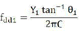
其中

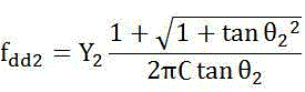
其中是谐振器的特性导纳;是半波长谐振器的电长度;C是变容二极管在不同电压下的电容值;在图5中显示了图3b中第二半波长谐振器的谐振频率、变容二极管的电容值C和微带线长度的关系,可以看出在长度10-18mm范围内谐振频率和电容值的关系特性与四分之一波长谐振器在长度6-8mm内的关系特性相似,当

当第一输入端口和第二输入端口输入共模信号时,整个滤波器在第一半波长谐振器和第三半波长谐振器的中点所在的直线位置上形成一个磁隔离墙。第一半波长谐振器和第三半波长谐振器在中间位置有电流流通,接在第一半波长谐振器和第三半波长谐振器中间加载的所述电容上有电流流通。第一半波长谐振器和第三半波长谐振器等效的两个四分之一波长的谐振器需要考虑中间加载的所述电容。共模信号时的实际工作等效滤波器结构如图6所示。图7给出了等效的四分之一波长的谐振器,谐振频率为: When the first input port and the second input port input a common mode signal, the entire filter forms a magnetic isolation wall at the linear position where the midpoints of the first half-wavelength resonator and the third half-wavelength resonator are located. The first half-wavelength resonator and the third half-wavelength resonator have a current flowing in the middle position, and the capacitor loaded between the first half-wavelength resonator and the third half-wavelength resonator has a current flowing through it. The two quarter-wavelength resonators equivalent to the first half-wavelength resonator and the third half-wavelength resonator need to consider the capacitance loaded in the middle. The actual working equivalent filter structure when the common mode signal is shown in Figure 6. Figure 7 shows an equivalent quarter-wavelength resonator with a resonant frequency of:
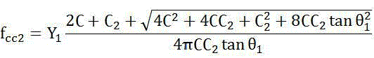
如图中所示, Y1是微带线的特性导纳;θ1微带线的电长度;C是变容二极管在不同电压下的电容值;C2是所述加载电容的电容值。 As shown in the figure, Y 1 is the characteristic admittance of the microstrip line; θ 1 is the electrical length of the microstrip line; C is the capacitance value of the varactor diode at different voltages; C 2 is the capacitance value of the loading capacitor.
由于加载的所述第二电容13和第三电容14的电容值大小不同,使得这两个谐振器的谐振频率不同,信号不能通过;共模信号就被抑制了。
Since the capacitance values of the
在图2和图6中可以看出,所述滤波器采用抽头线方式馈电。根据“R. J. Cameron, C. M. Kudsia, and R. R. Mansour, Microwave Filters for Communication Systems: Fundamentals, Design, and Applications, New York: Wiley: John Wiley & Sons, Inc, 2007.”所提供的分析可知,对于ABW,在某个恒定的绝对带宽,;滤波器实际外部品质因数

在下面实施例中,具有60MHz恒定绝对带宽的ABW制作在相对介电常数为10.2、厚度为0.63mm、损耗因子为0.0023的介质基板上。变容二极管选用东芝公司的硅变容二极管lsv277。 In the following embodiments, the ABW with a constant absolute bandwidth of 60 MHz is fabricated on a dielectric substrate with a relative permittivity of 10.2, a thickness of 0.63 mm, and a dissipation factor of 0.0023. The varactor diode is selected from Toshiba's silicon varactor diode lsv277. the
实施实例: 具有60MHz恒定绝对带宽的平衡式射频电调带通滤波器 Implementation Example: A Balanced RF Electrically Adjustable Bandpass Filter with a Constant Absolute Bandwidth of 60MHz
具有60MHz恒定绝对带宽的平衡式射频电调带通滤波器结构如图1所示。具体参数为:第一微带线2长度为10.2mm,宽度为0.8mm,第二微带线3长度为18.7mm,第五微带线8长度为24.1mm,宽度为0.8mm,第六微带线9长度为10.4mm,第八微带线16长度为3.3mm,宽度为0.6mm,第一电容15大小为7pF,第一半波长谐振器中间加载的所述第二电容13大小为20pF,第三半波长谐振器中间加载的所述第三电容14大小为7pF,第二微带线3和第五微带线8之间的距离为0.6mm。图8给出了利用上述参数所设计的滤波器进行仿真和实际测量的结果,其中仿真和实际测量分别是使用安捷伦公司的商业电磁仿真软件ADS和E5071C网络分析仪来完成。图8a为该滤波器差模工作情况下在四个特殊偏置电压时的仿真、计算及测试的传输特性,横轴表示频率,纵轴表示传输特性|Sdd21|。图8b所示为该滤波器的反射特性,横轴表示频率,纵轴表示回波损耗|Sdd11|。由图8a和图8b可见,滤波器的通带频率可以从549MHz调到775MHz,具有34.1%的相对调节范围。对所有的调谐状态,测量的带内插入损耗在3.5-4.2dB之间,回波损耗都低于-10dB。3dB带宽为60
本实用新型基于镜像对称的平衡结构,在差模和共模信号下具有不同的等效电路,具有恒定的绝对带宽,中间频率可调,在较宽的频带内抑制共模噪声。在频率调谐范围内带宽和通带波形保持恒定不变。通过调节设计的参数,可以调节带宽,即这种结构可以用来实现各种带宽规格。 The utility model is based on a mirror symmetrical balanced structure, has different equivalent circuits under differential mode and common mode signals, has constant absolute bandwidth, adjustable intermediate frequency, and suppresses common mode noise in a wider frequency band. The bandwidth and passband waveform remain constant over the frequency tuning range. By adjusting the parameters of the design, the bandwidth can be adjusted, that is, this structure can be used to achieve various bandwidth specifications. the
以上所述仅为本实用新型的较佳实例,并不用以限制本实用新型,凡在本实用新型的精神和原则之内,所作的任何修改、等同替换、改进等,均应包含在本实用新型的保护范围之内。 The above descriptions are only preferred examples of the present utility model, and are not intended to limit the present utility model. Any modifications, equivalent replacements, improvements, etc. made within the spirit and principles of the present utility model shall be included in the present utility model. within the scope of the new protection. the
Claims (6)
Priority Applications (1)
| Application Number | Priority Date | Filing Date | Title |
|---|---|---|---|
| CN2011201771732U CN202364184U (en) | 2011-05-27 | 2011-05-27 | Balanced radio frequency electric adjustment band pass filter with constant absolute bandwidth |
Applications Claiming Priority (1)
| Application Number | Priority Date | Filing Date | Title |
|---|---|---|---|
| CN2011201771732U CN202364184U (en) | 2011-05-27 | 2011-05-27 | Balanced radio frequency electric adjustment band pass filter with constant absolute bandwidth |
Publications (1)
| Publication Number | Publication Date |
|---|---|
| CN202364184U true CN202364184U (en) | 2012-08-01 |
Family
ID=46575338
Family Applications (1)
| Application Number | Title | Priority Date | Filing Date |
|---|---|---|---|
| CN2011201771732U Expired - Lifetime CN202364184U (en) | 2011-05-27 | 2011-05-27 | Balanced radio frequency electric adjustment band pass filter with constant absolute bandwidth |
Country Status (1)
| Country | Link |
|---|---|
| CN (1) | CN202364184U (en) |
Cited By (3)
| Publication number | Priority date | Publication date | Assignee | Title |
|---|---|---|---|---|
| CN102324599A (en) * | 2011-05-27 | 2012-01-18 | 华南理工大学 | Balanced type radio frequency voltage tunable bandpass filter with constant absolute bandwidth |
| CN103943919A (en) * | 2014-04-23 | 2014-07-23 | 西南交通大学 | Constant-bandwidth tunable bandpass filter |
| CN116800219A (en) * | 2023-07-20 | 2023-09-22 | 南通至晟微电子技术有限公司 | Circuit structure for balancing frequency adjustable to single-ended filtering power divider |
-
2011
- 2011-05-27 CN CN2011201771732U patent/CN202364184U/en not_active Expired - Lifetime
Cited By (6)
| Publication number | Priority date | Publication date | Assignee | Title |
|---|---|---|---|---|
| CN102324599A (en) * | 2011-05-27 | 2012-01-18 | 华南理工大学 | Balanced type radio frequency voltage tunable bandpass filter with constant absolute bandwidth |
| CN102324599B (en) * | 2011-05-27 | 2014-02-26 | 华南理工大学 | Balanced type radio frequency voltage tunable bandpass filter with constant absolute bandwidth |
| CN103943919A (en) * | 2014-04-23 | 2014-07-23 | 西南交通大学 | Constant-bandwidth tunable bandpass filter |
| CN103943919B (en) * | 2014-04-23 | 2016-06-01 | 西南交通大学 | The variable band-pass filter of a kind of constant bandwidth |
| CN116800219A (en) * | 2023-07-20 | 2023-09-22 | 南通至晟微电子技术有限公司 | Circuit structure for balancing frequency adjustable to single-ended filtering power divider |
| CN116800219B (en) * | 2023-07-20 | 2024-03-19 | 南通至晟微电子技术有限公司 | Frequency-adjustable balance to single-ended filtering power divider |
Similar Documents
| Publication | Publication Date | Title |
|---|---|---|
| CN102324599B (en) | Balanced type radio frequency voltage tunable bandpass filter with constant absolute bandwidth | |
| CN102280678B (en) | Balanced radio frequency electrically tunable bandpass filter with constant relative bandwidth | |
| CN101894995B (en) | Radio frequency electrically adjusted band-pass filter with constant absolute bandwidth | |
| US9515362B2 (en) | Tunable bandpass filter | |
| CN102403557B (en) | High-selectivity double band-pass filter with independent adjustable passband | |
| CN105529515B (en) | A kind of tunable band-pass bandstop filter based on open circuit minor matters loading | |
| CN102522615B (en) | Miniature dual-band band-pass filter with adjustable low band | |
| CN102403562A (en) | Powder divider integrating a dual-frequency bandpass filter | |
| CN102832434B (en) | Equal power splitter integrating band-pass filtering function | |
| CN105552494B (en) | A kind of adjustable plane bandpass and band-rejection filter | |
| CN203056058U (en) | Balanced RF ESC Bandpass Filter with Bandwidth Control | |
| CN110459839B (en) | A Frequency Tunable Differential Double Pass Band Filter | |
| WO2012060775A1 (en) | Miniaturized passive low pass filter | |
| CN103915669B (en) | Filtering power divider with double passing bands | |
| CN104821420B (en) | Reconfigurable dual-band-stop filter | |
| KR101313694B1 (en) | Harmonic suppressed dual-band bandpass filters with tunable passbands | |
| CN116722336A (en) | A filter power splitter based on copper-based micro-coaxial transmission line | |
| CN202373678U (en) | Miniaturized double-passband band-pass filter with adjustable low pass band | |
| CN110247143B (en) | A switchable and tunable microstrip bandpass filter | |
| CN202363564U (en) | Double-frequency band elimination filter | |
| CN202364184U (en) | Balanced radio frequency electric adjustment band pass filter with constant absolute bandwidth | |
| CN102386464B (en) | Double-frequency band elimination filter | |
| CN205646079U (en) | Adjustable plane band -pass - band elimination filter | |
| KR101546931B1 (en) | Triple-band bandstop filter | |
| CN107634293B (en) | A miniaturized microstrip low-pass filter with two transmission zeros |
Legal Events
| Date | Code | Title | Description |
|---|---|---|---|
| C14 | Grant of patent or utility model | ||
| GR01 | Patent grant | ||
| AV01 | Patent right actively abandoned |
Granted publication date: 20120801 Effective date of abandoning: 20140226 |
|
| RGAV | Abandon patent right to avoid regrant |