CN102315246A - Relaxation SiGe virtual substrate and preparation method thereof - Google Patents
Relaxation SiGe virtual substrate and preparation method thereof Download PDFInfo
- Publication number
- CN102315246A CN102315246A CN2010102146669A CN201010214666A CN102315246A CN 102315246 A CN102315246 A CN 102315246A CN 2010102146669 A CN2010102146669 A CN 2010102146669A CN 201010214666 A CN201010214666 A CN 201010214666A CN 102315246 A CN102315246 A CN 102315246A
- Authority
- CN
- China
- Prior art keywords
- sige
- buffer layer
- layer
- composition
- substrate
- Prior art date
- Legal status (The legal status is an assumption and is not a legal conclusion. Google has not performed a legal analysis and makes no representation as to the accuracy of the status listed.)
- Granted
Links
- 229910000577 Silicon-germanium Inorganic materials 0.000 title claims abstract description 143
- 238000002360 preparation method Methods 0.000 title claims abstract description 19
- 239000000203 mixture Substances 0.000 claims abstract description 98
- 239000000758 substrate Substances 0.000 claims abstract description 87
- 239000000463 material Substances 0.000 claims abstract description 18
- 238000000034 method Methods 0.000 claims abstract description 14
- 238000005229 chemical vapour deposition Methods 0.000 claims abstract description 3
- 230000006837 decompression Effects 0.000 claims abstract description 3
- 239000002243 precursor Substances 0.000 claims description 26
- 239000007789 gas Substances 0.000 claims description 22
- 239000012159 carrier gas Substances 0.000 claims description 18
- 238000000137 annealing Methods 0.000 claims description 12
- 239000013078 crystal Substances 0.000 claims description 6
- 238000011065 in-situ storage Methods 0.000 claims description 6
- 230000007423 decrease Effects 0.000 claims description 2
- 229910052732 germanium Inorganic materials 0.000 abstract description 47
- GNPVGFCGXDBREM-UHFFFAOYSA-N germanium atom Chemical compound [Ge] GNPVGFCGXDBREM-UHFFFAOYSA-N 0.000 abstract description 34
- 238000005516 engineering process Methods 0.000 abstract description 16
- 239000004065 semiconductor Substances 0.000 abstract description 12
- 230000007547 defect Effects 0.000 description 16
- 238000012360 testing method Methods 0.000 description 15
- 235000012431 wafers Nutrition 0.000 description 10
- 238000012545 processing Methods 0.000 description 7
- 230000005540 biological transmission Effects 0.000 description 5
- 238000005530 etching Methods 0.000 description 5
- QUZPNFFHZPRKJD-UHFFFAOYSA-N germane Chemical compound [GeH4] QUZPNFFHZPRKJD-UHFFFAOYSA-N 0.000 description 5
- 229910052986 germanium hydride Inorganic materials 0.000 description 5
- 238000002017 high-resolution X-ray diffraction Methods 0.000 description 5
- 230000003287 optical effect Effects 0.000 description 4
- 238000012876 topography Methods 0.000 description 4
- 229910003818 SiH2Cl2 Inorganic materials 0.000 description 3
- 238000000407 epitaxy Methods 0.000 description 3
- 238000011161 development Methods 0.000 description 2
- 230000018109 developmental process Effects 0.000 description 2
- 238000004377 microelectronic Methods 0.000 description 2
- 238000011160 research Methods 0.000 description 2
- 239000000969 carrier Substances 0.000 description 1
- 239000000084 colloidal system Substances 0.000 description 1
- 238000010586 diagram Methods 0.000 description 1
- 230000009977 dual effect Effects 0.000 description 1
- 230000012447 hatching Effects 0.000 description 1
- 238000005498 polishing Methods 0.000 description 1
- 238000001228 spectrum Methods 0.000 description 1
- 239000000126 substance Substances 0.000 description 1
- 230000003746 surface roughness Effects 0.000 description 1
Images


Landscapes
- Recrystallisation Techniques (AREA)
Abstract
本发明属于半导体材料技术领域,涉及一种弛豫高锗含量的SiGe虚拟衬底及其制备方法。该SiGe虚拟衬底包括Si衬底、在Si衬底上由内而外依次外延生长的Ge晶籽层、Ge缓冲层、组份渐变的SiGe缓冲层和组分恒定的SiGe层;所述Ge晶籽层和所述Ge缓冲层组成Ge驰豫缓冲层。该SiGe虚拟衬底具有高Ge含量、完全弛豫、位错密度低、厚度薄、表面平整等特性。该SiGe虚拟衬底的制备方法为采用减压化学气相沉积法在Si衬底上依次生长各外延层。本发明所制备的弛豫高锗含量的SiGe虚拟衬底,可广泛应用于CMOS工艺中Ge沟道应变工程和高迁移率沟道材料制备上,进一步提高CMOS器件的性能。
The invention belongs to the technical field of semiconductor materials, and relates to a relaxed SiGe dummy substrate with high germanium content and a preparation method thereof. The SiGe virtual substrate includes a Si substrate, a Ge seed layer epitaxially grown on the Si substrate from inside to outside, a Ge buffer layer, a SiGe buffer layer with a graded composition, and a SiGe layer with a constant composition; the Ge The seed layer and the Ge buffer layer constitute a Ge relaxation buffer layer. The SiGe virtual substrate has the characteristics of high Ge content, complete relaxation, low dislocation density, thin thickness, smooth surface and the like. The preparation method of the SiGe dummy substrate is to sequentially grow each epitaxial layer on the Si substrate by adopting a decompression chemical vapor deposition method. The relaxed SiGe virtual substrate with high germanium content prepared by the invention can be widely used in Ge channel strain engineering and high mobility channel material preparation in CMOS technology, and further improves the performance of CMOS devices.
Description
技术领域 technical field
本发明属于半导体材料技术领域,涉及一种高质量的弛豫高锗含量的SiGe虚拟衬底及其制备方法。 The invention belongs to the technical field of semiconductor materials, and relates to a high-quality relaxed SiGe dummy substrate with high germanium content and a preparation method thereof. the
背景技术 Background technique
在半导体产业中,Si材料作为占据统治地位的半导体器件已经发展了近半个世纪。随着科学技术的发展以及人们对微电子器件性能的追求,使得半导体器件的特征尺寸不断缩小,单个晶体管尺寸逐渐达到了物理和技术的双重极限,以传统Si作为沟道材料的CMOS器件的性能已经无法满足半导体器件性能不断提升的要求。人们正在加紧寻找新型方法和材料,以保持微电子器件快速增长的步伐。现已公知,在CMOS器件中引入应变的Si或Ge可以显著提高器件的性能,因为处于应变状态下的Si和Ge的载流子迁移率可显著提高。应变Si和应变Ge被认为是最有前途的沟道材料。由于Ge和Si之间存在较大的品格失配(4.2%),不能直接将Ge外延生长在Si晶圆上或者直接将Si外延生长在Ge晶圆上引入应变用作沟道材料,他们之间的品格失配使得外延层非常薄时就会发生弛豫,产生缺陷和位错,严重降低载流子的迁移率。因此,就需要开发新的技术,在Si衬底上得到高质量、适于沟道材料用的缓冲层。虚拟衬底的开发被认为是一种非常有前景的研究项目。虚拟衬底一般是通过各种方法在Si衬底上获得一层高质量的、与所需沟道材料性质差别较小的膜层,做为新材料的衬底,在其上制备高质量的沟道材料层。如果引入应变的Si作为沟道材料,就需要高质量低锗含量的SiGe虚拟衬底;如果引入应变的Ge作为沟道材料,就需要高质量高锗含量的SiGe虚拟衬底。传统的制备虚拟衬底的方法主要是通过外延组份渐变的SiGe层得到虚拟衬底,这在低锗含量的SiGe虚拟衬底上是可行的,但是如果制备高锗含量的虚拟衬底,就需要十分厚的SiGe组份渐变层。如通过SiGe组份渐变层制备的Si1-xGex(0.7≤x≤0.9)虚拟衬底厚度多在5μm以上,有的甚至10μm,导致加工时间长,成本较高,而且较厚的SiGe组份渐变层使虚拟衬底表面具有严重的交叉影线(cross hatch),使得表面粗 糙度较大,需要化学机械抛光(CMP)才能得到比较平坦的表面,增加了工艺的复杂性。因此,获得高质量的高锗含量的薄SiGe虚拟衬底仍是Si基半导体材料制备领域的一个具有实际应用的研究热点。 In the semiconductor industry, Si material has been developed as a dominant semiconductor device for nearly half a century. With the development of science and technology and people's pursuit of the performance of microelectronic devices, the feature size of semiconductor devices has been continuously reduced, and the size of a single transistor has gradually reached the dual limits of physics and technology. The performance of CMOS devices using traditional Si as the channel material It has been unable to meet the requirements of continuous improvement in the performance of semiconductor devices. People are stepping up the search for new methods and materials to maintain the pace of rapid growth of microelectronic devices. It is known that introducing strained Si or Ge into a CMOS device can significantly improve the performance of the device, because the carrier mobility of Si and Ge under strain can be significantly improved. Strained Si and strained Ge are considered to be the most promising channel materials. Due to the large lattice mismatch (4.2%) between Ge and Si, it is not possible to directly epitaxially grow Ge on Si wafers or directly grow Si epitaxially on Ge wafers to introduce strain as channel material, between them The lattice mismatch between them makes the epitaxial layer relax when it is very thin, resulting in defects and dislocations, which seriously reduce the mobility of carriers. Therefore, it is necessary to develop new technologies to obtain high-quality buffer layers suitable for channel materials on Si substrates. The development of virtual substrates is considered a very promising research project. The virtual substrate generally obtains a layer of high-quality film layer on the Si substrate through various methods, which is less different from the properties of the required channel material, as the substrate of the new material, and prepares a high-quality layer of channel material. If strained Si is used as the channel material, a SiGe virtual substrate with high quality and low germanium content is required; if strained Ge is introduced as the channel material, a SiGe virtual substrate with high quality and high germanium content is required. The traditional method of preparing a dummy substrate is mainly to obtain a dummy substrate by epitaxy of a SiGe layer with a gradient composition, which is feasible on a SiGe dummy substrate with a low germanium content, but if a dummy substrate with a high germanium content is prepared, it will be difficult A very thick SiGe composition graded layer is required. For example, the virtual substrate thickness of Si 1-x Ge x (0.7≤x≤0.9) prepared by SiGe composition graded layer is more than 5 μm, and some even 10 μm, resulting in long processing time and high cost, and thicker SiGe The graded composition layer makes the surface of the virtual substrate have severe cross hatching (cross hatch), making the surface rougher, requiring chemical mechanical polishing (CMP) to obtain a relatively flat surface, which increases the complexity of the process. Therefore, obtaining high-quality thin SiGe virtual substrates with high germanium content is still a research hotspot with practical applications in the field of Si-based semiconductor material preparation.
发明内容 Contents of the invention
本发明的目的是提供一种弛豫高锗含量的SiGe虚拟衬底及其制备方法,以克服现有技术中所制备的高锗含量SiGe虚拟衬底的厚度大、表面粗糙、工艺复杂等缺点。本发明提供的一种以反向渐变SiGe组份中Ge含量的方式,制备了高质量的SiGe虚拟衬底,该虚拟衬底具有高Ge含量、完全弛豫、位错密度低、厚度薄、表面平整等特性。 The purpose of the present invention is to provide a SiGe virtual substrate with a relaxed high germanium content and a preparation method thereof, so as to overcome the shortcomings of the SiGe virtual substrate with a high germanium content prepared in the prior art such as large thickness, rough surface, and complicated process. . The present invention provides a high-quality SiGe dummy substrate prepared by reversely changing the Ge content in the SiGe composition. The dummy substrate has high Ge content, complete relaxation, low dislocation density, thin thickness, Features such as smooth surface. the
为了解决上述技术问题,本发明的技术方案如下: In order to solve the problems of the technologies described above, the technical scheme of the present invention is as follows:
一种弛豫SiGe虚拟衬底,所述SiGe虚拟衬底包括Si衬底、在Si衬底上由内而外依次外延生长的Ge晶籽层、Ge缓冲层、组份渐变的SiGe缓冲层和组分恒定的SiGe层,所述Ge晶籽层和所述Ge缓冲层组成Ge弛豫缓冲层。 A kind of relaxed SiGe dummy substrate, described SiGe dummy substrate comprises Si substrate, the Ge crystal seed layer that grows epitaxially from inside to outside on Si substrate successively, Ge buffer layer, the SiGe buffer layer of composition gradient and The SiGe layer with constant composition, the Ge seed layer and the Ge buffer layer constitute a Ge relaxation buffer layer. the
所述Si衬底上各外延生长层均为完全应变弛豫的缓冲层。 Each epitaxial growth layer on the Si substrate is a fully strain-relaxed buffer layer. the
所述弛豫高锗含量的SiGe虚拟衬底中的位错和缺陷主要集中在组份渐变的SiGe缓冲层中,组分恒定的SiGe层中具有较低的位错和缺陷密度(<106cm-2)。 The dislocations and defects in the relaxed SiGe dummy substrate with high germanium content are mainly concentrated in the SiGe buffer layer with a graded composition, and the SiGe layer with a constant composition has a lower dislocation and defect density (<10 6 cm -2 ).
所述弛豫SiGe虚拟衬底中锗的摩尔百分含量为Ge%≥70%,为高锗含量的SiGe虚拟衬底。 The mole percentage of germanium in the relaxed SiGe dummy substrate is Ge%≥70%, which is a SiGe dummy substrate with high germanium content. the
所述弛豫SiGe虚拟衬底的平均粗糙度为1.3-1.9nm,低于现有技术工艺水平的要求(<2.0nm)。通过刻蚀所述弛豫高锗含量的SiGe虚拟衬底后的位错密度在106cm-2的量级,满足半导体器件加工工艺对衬底的要求。 The average roughness of the relaxed SiGe dummy substrate is 1.3-1.9nm, which is lower than the requirement of the prior art technology level (<2.0nm). The dislocation density after etching the relaxed SiGe dummy substrate with high germanium content is on the order of 10 6 cm -2 , which meets the requirements of the semiconductor device processing technology for the substrate.
所述SiGe虚拟衬底中Si衬底采用Si晶圆;所述Si晶圆片为标准尺寸的工业化晶片,该Si晶圆片的尺寸大小选自4英寸、6英寸、8英寸、12英寸等尺寸规格。 The Si substrate in the SiGe virtual substrate adopts a Si wafer; the Si wafer is an industrial wafer of a standard size, and the size of the Si wafer is selected from 4 inches, 6 inches, 8 inches, 12 inches, etc. Dimensions. the
所述SiGe虚拟衬底中Ge晶籽层和Ge缓冲层组成完全驰豫的Ge驰豫缓冲层;所述 Ge晶籽层的厚度为50-100nm,所述Ge缓冲层的厚度为300-600nm,所述整个Ge驰豫缓冲层的厚度为350-700nm。 The Ge seed layer and the Ge buffer layer in the SiGe virtual substrate form a fully relaxed Ge relaxation buffer layer; the thickness of the Ge seed layer is 50-100nm, and the thickness of the Ge buffer layer is 300-600nm , the thickness of the whole Ge relaxation buffer layer is 350-700nm. the
所述组份渐变的SiGe缓冲层和组分恒定的SiGe层中组分为Si和Ge,其各自含量为摩尔百分含量。 The components in the SiGe buffer layer with gradual composition and the SiGe layer with constant composition are Si and Ge, and their respective contents are in mole percent. the
所述组份渐变的SiGe缓冲层中,以紧邻Ge弛豫缓冲层的侧面为起点、以紧邻组分恒定的SiGe层的侧面为终点,Ge的摩尔百分含量从100%逐渐减少至与组分恒定的SiGe层中的Ge摩尔百分含量相同。在所述的组份渐变的SiGe缓冲层中,所述Ge的摩尔百分含量每200-250nm厚度变化5%的Ge含量。 In the SiGe buffer layer with gradually changing composition, starting from the side adjacent to the Ge relaxation buffer layer and ending at the side adjacent to the SiGe layer with constant composition, the mole percentage of Ge gradually decreases from 100% to the composition The Ge mole percentage content in the constant SiGe layer is the same. In the SiGe buffer layer with graded composition, the mole percentage of Ge varies by 5% of the Ge content per 200-250 nm thickness. the
如,所述组份渐变的SiGe缓冲层的Ge的摩尔百分含量随着组份渐变的SiGe缓冲层厚度的增加,从100%开始渐变到95%,从95%渐变到90%,以此类推,每200-250nm厚度减少5%的Ge含量,直至渐变到与紧邻的组分恒定的SiGe层中的Ge的摩尔百分含量相同。 For example, the mole percentage of Ge in the SiGe buffer layer with a graded composition gradually changes from 100% to 95% and from 95% to 90% as the thickness of the SiGe buffer layer with a graded composition increases. By analogy, the Ge content is reduced by 5% every 200-250 nm thickness until it gradually becomes the same as the Ge content in the next SiGe layer with constant composition. the
所述组分恒定的SiGe层的厚度为500-1000nm,可以根据所需的虚拟衬底的厚度要求来调节。 The thickness of the SiGe layer with constant composition is 500-1000 nm, which can be adjusted according to the required thickness of the virtual substrate. the
所述SiGe组份恒定层上可外延生长应变Ge沟道层以用于CMOS器件中的沟道材料。 A strained Ge channel layer can be epitaxially grown on the SiGe constant composition layer for use as a channel material in a CMOS device. the
一种弛豫高锗含量的SiGe虚拟衬底的制备方法,根据所述的弛豫高锗含量的SiGe虚拟衬底的组成采用减压化学气相沉积法在Si衬底上、以GeH4和SiH2Cl2为气相前驱物、以H2为载气依次生长各外延层。 A preparation method of a SiGe dummy substrate with a relaxed high germanium content, according to the composition of the SiGe dummy substrate with a relaxed high germanium content, the decompression chemical vapor deposition method is used on the Si substrate, with GeH 4 and SiH 2 Cl 2 is used as the gas phase precursor, and H 2 is used as the carrier gas to grow each epitaxial layer sequentially.
所述的弛豫高锗含量的SiGe虚拟衬底的制备方法中Ge晶籽层和Ge缓冲层的外延生长均以GeH4为气相前驱物,所述组份渐变的SiGe缓冲层和组份恒定的SiGe层的外延生长均以GeH4和SiH2Cl2为气相前驱物。 In the preparation method of the SiGe virtual substrate with high germanium content in the relaxation, the epitaxial growth of the Ge seed layer and the Ge buffer layer all use GeH4 as a gas phase precursor, and the SiGe buffer layer with a gradual composition and a constant composition The epitaxial growth of the SiGe layer used GeH 4 and SiH 2 Cl 2 as gas phase precursors.
该制备方法具体包括如下步骤: The preparation method specifically includes the following steps:
1)在Si衬底上外延生长Ge晶籽层,所述的Ge晶籽层的生长温度为350-400℃,生长室压力为50-150Torr,生长的厚度为50-100nm。 1) Epitaxially growing a Ge seed layer on a Si substrate, the growth temperature of the Ge seed layer is 350-400° C., the growth chamber pressure is 50-150 Torr, and the growth thickness is 50-100 nm. the
所述的Ge晶籽层的生长以GeH4为气相前驱物,流速为100-200sccm,以H2为载气。 The growth of the Ge seed layer uses GeH 4 as a gas phase precursor, a flow rate of 100-200 sccm, and H 2 as a carrier gas.
2)在生长好的Ge晶籽层上外延生长Ge缓冲层,所述的Ge缓冲层的生长温度为650-700℃,生长室压力为50-150Torr,生长的厚度为300-600nm。 2) Epitaxially growing a Ge buffer layer on the grown Ge seed layer, the growth temperature of the Ge buffer layer is 650-700° C., the growth chamber pressure is 50-150 Torr, and the growth thickness is 300-600 nm. the
所述的Ge缓冲层的生长以GeH4为气相前驱物,流速为100-200sccm,以H2为载气。 The growth of the Ge buffer layer uses GeH 4 as a gas phase precursor, a flow rate of 100-200 sccm, and H 2 as a carrier gas.
3)所述步骤2)的Ge缓冲层生长完成后在生长室原位退火,退火温度为800-900℃,获得完全弛豫的Ge弛豫缓冲层。 3) In-situ annealing in the growth chamber after the growth of the Ge buffer layer in step 2), the annealing temperature is 800-900° C. to obtain a fully relaxed Ge buffer layer. the
所述的Ge弛豫缓冲层的厚度为350-700nm,可以根据所需的虚拟衬底的厚度要求来调节; The thickness of the Ge relaxation buffer layer is 350-700nm, which can be adjusted according to the thickness requirements of the required virtual substrate;
所述的退火时间,如可以为10分钟。 The annealing time may be, for example, 10 minutes. the
4)在生长好的Ge弛豫缓冲层上外延生长组份渐变的SiGe缓冲层,所述的外延生长温度为800-900℃,生长室压力为20-100Torr。 4) Epitaxially growing a SiGe buffer layer with a graded composition on the grown Ge relaxation buffer layer, the epitaxial growth temperature is 800-900° C., and the growth chamber pressure is 20-100 Torr. the
所述组份渐变的SiGe缓冲层的生长以H2为载气,以GeH4和SiH2Cl2为气相前驱物,通过在外延生长过程中动态调节所述气相前驱物GeH4和SiH2Cl2的流速比来制备。 The growth of the composition-graded SiGe buffer layer uses H2 as the carrier gas and GeH4 and SiH2Cl2 as the gaseous precursors, and dynamically adjusts the gaseous precursors GeH4 and SiH2Cl during the epitaxial growth process 2 flow rate ratio to prepare.
5)在生长好的组份渐变的SiGe缓冲层上外延生长组份恒定的SiGe层,所述的外延生长温度为800-900℃,生长室压力为20-100Torr,生长的厚度为500-1000nm。 5) Epitaxially grow a SiGe layer with a constant composition on the grown SiGe buffer layer with a gradient composition, the epitaxial growth temperature is 800-900°C, the growth chamber pressure is 20-100Torr, and the growth thickness is 500-1000nm . the
所述的组份恒定的SiGe层以H2为载气,以GeH4和SiH2Cl2为气相前驱物,GeH4的流量为300-500sccm,SiH2Cl2的流量为14-80sccm; The SiGe layer with constant composition uses H2 as carrier gas, GeH4 and SiH2Cl2 as gas phase precursors, the flow rate of GeH4 is 300-500sccm , and the flow rate of SiH2Cl2 is 14-80sccm;
其中所述SiH2Cl2的流量优选为14-62sccm。 Wherein the flow rate of SiH 2 Cl 2 is preferably 14-62 sccm.
本发明的弛豫高锗含量的SiGe虚拟衬底的制备方法中,其中所述整个Ge弛豫缓冲层是为外延生长组份渐变的SiGe缓冲层的必须条件,因此获得Ge弛豫缓冲层也是影响虚拟衬底质量的关键因素之一。整个Ge弛豫缓冲层中Ge晶籽层的外延生长温度不能过低,否 则会发生多晶生长,整个Ge弛豫缓冲层的厚度可以根据虚拟衬底的厚度要求在一定范围内调节; In the preparation method of the SiGe dummy substrate of relaxation high germanium content of the present invention, wherein said whole Ge relaxation buffer layer is the necessary condition for the SiGe buffer layer of epitaxial growth composition gradient, so obtaining Ge relaxation buffer layer is also One of the key factors affecting the quality of the virtual substrate. The epitaxial growth temperature of the Ge seed layer in the entire Ge relaxation buffer layer cannot be too low, otherwise polycrystalline growth will occur, and the thickness of the entire Ge relaxation buffer layer can be adjusted within a certain range according to the thickness requirements of the virtual substrate;
其中所述的组份渐变的SiGe缓冲层是本发明所述的高质量的SiGe虚拟衬底的最关键部分,随着组份渐变的SiGe缓冲层厚度的增加,组份渐变的SiGe缓冲层中每200-250nm厚度实现5%Ge含量的变化,过快或过慢的Ge组份渐变率对虚拟衬底质量和总厚度影响很大,这一缓冲层是限制虚拟衬底中位错和缺陷的区域; The SiGe buffer layer whose composition is gradually changed is the most critical part of the high-quality SiGe virtual substrate of the present invention. Every 200-250nm thickness changes 5% Ge content. Too fast or too slow Ge composition gradient rate has a great impact on the quality and total thickness of the virtual substrate. This buffer layer is to limit the dislocations and defects in the virtual substrate. Area;
其中所述组份恒定的SiGe缓冲层是完全弛豫的缓冲层,一般在高温下外延生长可以获得完全弛豫的SiGe层,外延生长温度为800-900℃,低温生长则需要退火工艺,且生长速率慢。 The SiGe buffer layer with a constant composition is a fully relaxed buffer layer. Generally, a fully relaxed SiGe layer can be obtained by epitaxial growth at a high temperature. The epitaxial growth temperature is 800-900° C., and an annealing process is required for low temperature growth, and Growth rate is slow. the
本发明的弛豫高锗含量的SiGe虚拟衬底,通过引入Ge晶籽层和Ge缓冲层所组成的Ge弛豫缓冲层,采用反向渐变组份渐变的SiGe缓冲层中Ge的含量来限制位错和缺陷,特别适合制备高锗含量的薄SiGe虚拟衬底。采用本发明的制备方法不仅可以获得厚度较薄的高锗含量的SiGe虚拟衬底,同时有效地减小了该SiGe虚拟衬底的表面粗糙度和位错密度,不需要额外的加工工艺,如CMP等,缩短了外延时间,节省成本。本发明所制备的高质量SiGe虚拟衬底,具有高Ge含量、完全弛豫、位错密度低、厚度薄、表面平整等特性,达到了器件级应变Ge沟道材料的应用要求。 The relaxed SiGe dummy substrate with high germanium content of the present invention is limited by introducing the Ge relaxation buffer layer composed of the Ge seed layer and the Ge buffer layer, and adopting the content of Ge in the SiGe buffer layer with reverse gradient composition. Dislocations and defects, especially suitable for preparing thin SiGe virtual substrates with high germanium content. Adopting the preparation method of the present invention can not only obtain the SiGe dummy substrate with thinner thickness and high germanium content, but also effectively reduce the surface roughness and dislocation density of the SiGe dummy substrate without additional processing technology, such as CMP, etc. shorten the epitaxy time and save costs. The high-quality SiGe virtual substrate prepared by the invention has the characteristics of high Ge content, complete relaxation, low dislocation density, thin thickness, flat surface, etc., and meets the application requirements of device-level strained Ge channel materials. the
附图说明 Description of drawings
图1本发明的高锗含量SiGe虚拟衬底的结构示意图及制备流程图 Fig. 1 is a schematic structural representation and a preparation flow chart of the high germanium content SiGe dummy substrate of the present invention
图2实施例1中Si0.2Ge0.8虚拟衬底c高分辨X射线衍射倒易空间图谱 Fig. 2 High-resolution X-ray diffraction reciprocal space pattern of Si 0.2 Ge 0.8 virtual substrate c in Example 1
图3实施例1中Si0.2Ge0.8虚拟衬底c横截面透射电子显微镜(TEM)照片 Figure 3 Transmission electron microscope (TEM) photograph of the cross-section of Si 0.2 Ge 0.8 virtual substrate c in Example 1
图4实施例1中Si0.2Ge0.8虚拟衬底c的表面原子力显微镜(AFM)照片 Surface atomic force microscope (AFM) photo of Si 0.2 Ge 0.8 virtual substrate c in Fig. 4 embodiment 1
图5实施例1中Si0.2Ge0.8虚拟衬底c经刻蚀后的光学显微镜照片 Fig. 5 Optical microscope photo of Si 0.2 Ge 0.8 dummy substrate c etched in Example 1
具体实施方式 Detailed ways
下面结合具体实施例进一步阐述本发明,应理解,这些实施例仅用于说明本发明而不用于限制本发明的保护范围。 The present invention will be further described below in conjunction with specific examples. It should be understood that these examples are only used to illustrate the present invention and are not intended to limit the protection scope of the present invention. the
实施例1Example 1
一种高锗含量的SiGe虚拟衬底的制备流程如图1所示,以制备Si0.2Ge0.8虚拟衬底为例,包括以下步骤: The preparation process of a SiGe dummy substrate with high germanium content is shown in Figure 1. Taking the preparation of Si 0.2 Ge 0.8 dummy substrate as an example, it includes the following steps:
步骤s100,分别准备四片4英寸、6英寸、8英寸和12英寸的Si晶圆片作为Si衬底。 In step s100, four 4-inch, 6-inch, 8-inch and 12-inch Si wafers are respectively prepared as Si substrates. the
步骤s101,Ge弛豫缓冲层的生长:分别以4英寸、6英寸、8英寸和12英寸的Si衬底为基础,先在400℃以GeH4为气相前驱物,GeH4流量为150sccm,以H2为载气,生长室压力为100Torr,分别沉积一层厚度为50nm、60nm、100nm、和100nm的Ge晶籽层;保持生长气氛不变,然后在沉积好的四片Ge晶籽层上在700℃分别沉积厚度为300nm、340nm、400nm和600nm的Ge缓冲层,完成后均在850℃原位(外延生长室)退火10分钟,退火时保持生长室压力为100Torr,获得四片完全应变弛豫的Ge弛豫缓冲层。该四片Ge弛豫缓冲层分别为4英寸Si衬底350nm厚度的Ge弛豫缓冲层,标记为a1、6英寸Si衬底400nm厚度的Ge弛豫缓冲层,标记为b1、8英寸Si衬底500nm厚度的Ge弛豫缓冲层,标记为c1和12英寸Si衬底700nm厚度的Ge弛豫缓冲层,标记为d1。 Step s101, growth of Ge relaxation buffer layer: based on 4-inch, 6-inch, 8-inch and 12-inch Si substrates, respectively, at 400 ° C with GeH 4 as the gas phase precursor, the GeH 4 flow rate is 150 sccm, and H2 is the carrier gas, the pressure of the growth chamber is 100Torr, deposit a layer of Ge seed layer with a thickness of 50nm, 60nm, 100nm, and 100nm respectively; keep the growth atmosphere unchanged, and then deposit on the deposited four Ge seed layers Ge buffer layers with a thickness of 300nm, 340nm, 400nm and 600nm were deposited at 700°C, and annealed in situ (epitaxy growth chamber) at 850°C for 10 minutes after completion, and the growth chamber pressure was kept at 100 Torr during annealing to obtain four fully strained Relaxed Ge relaxation buffer layer. The four Ge relaxation buffer layers are respectively a Ge relaxation buffer layer with a thickness of 350 nm on a 4-inch Si substrate, marked as a1, a Ge relaxation buffer layer with a thickness of 400 nm on a 6-inch Si substrate, marked as b1, and an 8-inch Si substrate. The Ge relaxation buffer layer with a thickness of 500 nm is marked as c1 and the Ge relaxation buffer layer with a thickness of 700 nm on the 12-inch Si substrate is marked as d1.
步骤s102,组份渐变的SiGe缓冲层的生长:在步骤s101获得的弛豫Ge缓冲层a1、b1、c1和d1的基础上,分别外延生长组份渐变的SiGe缓冲层,以H2为载气,GeH4和SiCl2H2为气相前驱物,生长温度为850℃,生长室压力为20Torr,随组份渐变的SiGe缓冲层中Ge含量的变化,通过调节GeH4与SiH2Cl2流量比实现SiGe组份渐变,GeH4的流量保持在500sccm,SiCl2H2的流量随生长时间线性渐增。组份渐变的SiGe缓冲层每250nm厚度实现5%Ge的减少,直到渐变到Ge和Si的含量比为0.8∶0.2为止,分别得到厚度均为1000nm的组份渐变的Si0.2Ge0.8缓冲层a2、b2、c2和d2。 Step s102, growth of SiGe buffer layer with graded composition: on the basis of the relaxed Ge buffer layers a1, b1, c1 and d1 obtained in step s101, respectively epitaxially grow SiGe buffer layers with graded composition, with H2 as the carrier Gas, GeH 4 and SiCl 2 H 2 are gaseous precursors, the growth temperature is 850°C, the growth chamber pressure is 20Torr, the change of Ge content in the SiGe buffer layer with gradual composition changes, by adjusting the flow rate of GeH 4 and SiH 2 Cl 2 Ratio realizes the gradual change of SiGe composition, the flow rate of GeH 4 is kept at 500 sccm, and the flow rate of SiCl 2 H 2 increases linearly with the growth time. The composition-graded SiGe buffer layer realizes the reduction of 5% Ge every 250nm thickness, until the content ratio of Ge and Si is gradually changed to 0.8:0.2, and the composition-graded Si 0.2 Ge 0.8 buffer layer a2 with a thickness of 1000nm is obtained respectively , b2, c2 and d2.
步骤s103,组份恒定的SiGe层的生长:在步骤s102获得的组份渐变的Si0.2Ge0.8缓冲层 a2、b2、c2和d2的基础上,均以GeH4和SiCl2H2为气相前驱物,GeH4流量为500sccm,SiCl2H2流量为33sccm,H2为载气,外延生长温度为850℃,生长室压力为20Torr,生长厚度为500nm的组份恒定的Si0.2Ge0.8层,分别得到弛豫高锗含量的SiGe虚拟衬底a、b、c和d,经检测其外延层的总厚度分别为1850nm、1900nm、2000nm和2200nm。 Step s103, growth of a SiGe layer with a constant composition: on the basis of the Si 0.2 Ge 0.8 buffer layers a2, b2, c2 and d2 obtained in step s102 with a gradient composition, GeH 4 and SiCl 2 H 2 are used as gas phase precursors The GeH 4 flow rate is 500 sccm, the SiCl 2 H 2 flow rate is 33 sccm, H 2 is the carrier gas, the epitaxial growth temperature is 850 ° C, the growth chamber pressure is 20 Torr, and the growth thickness is 500 nm Si 0.2 Ge 0.8 layer with constant composition, Relaxed SiGe virtual substrates a, b, c and d with high germanium content were respectively obtained, and the total thickness of the epitaxial layer was detected to be 1850nm, 1900nm, 2000nm and 2200nm respectively.
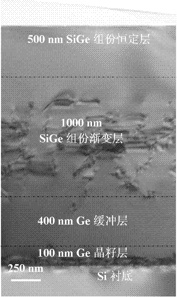
该实施例1所得的弛豫高锗含量的SiGe虚拟衬底的结构示意图如图1所示,以Si衬底为基础,由内而外依次外延生长的Ge晶籽层、Ge缓冲层、组份渐变的SiGe缓冲层和组分恒定的SiGe层,所述Ge晶籽层和所述Ge缓冲层组成Ge驰豫缓冲层。 The schematic diagram of the structure of the relaxed SiGe dummy substrate with high germanium content obtained in Example 1 is shown in FIG. A SiGe buffer layer with a graded composition and a SiGe layer with a constant composition, the Ge seed layer and the Ge buffer layer form a Ge relaxed buffer layer. the
图2为实施例1所得的Si0.2Ge0.8虚拟衬底c高分辨X射线衍射倒易空间图谱,外延生长的各层已在图中标出,可以看出Ge晶籽层和Ge缓冲层已发生完全应变弛豫,SiGe组份渐变层和SiGe组份恒定层也处于完全弛豫状态。 Figure 2 is the high-resolution X-ray diffraction reciprocal space map of the Si 0.2 Ge 0.8 virtual substrate c obtained in Example 1. The layers of epitaxial growth have been marked in the figure, and it can be seen that the Ge seed layer and the Ge buffer layer have occurred Complete strain relaxation, the SiGe composition graded layer and the SiGe composition constant layer are also in a complete relaxation state.
图3为实施例1所得的Si0.2Ge0.8虚拟衬底c横截面透射电子显微镜(TEM)照片,从图3中的TEM照片可以看出,Si0.2Ge0.8虚拟衬底c的各外延层总厚度为2μm,位错和缺陷主要集中在厚度为1μm的Si0-0.2Ge1-0.8组份渐变层,Si0.2Ge0.8组份恒定层中则没有明显的位错和缺陷。另外需要说明的是图3中组分恒定的SiGe层上面部分为制备透射电镜样品用的胶体,以作为最顶层的参照物。 Fig. 3 is the cross-sectional transmission electron microscope (TEM) photo of Si 0.2 Ge 0.8 dummy substrate c obtained in Example 1, as can be seen from the TEM photo in Fig. 3, each epitaxial layer of Si 0.2 Ge 0.8 dummy substrate c is total When the thickness is 2μm, the dislocations and defects are mainly concentrated in the Si 0-0.2 Ge 1-0.8 composition gradient layer with a thickness of 1μm, while there are no obvious dislocations and defects in the Si 0.2 Ge 0.8 constant composition layer. In addition, it should be noted that the upper part of the SiGe layer with a constant composition in Figure 3 is the colloid used to prepare the TEM sample, as a reference for the topmost layer.
图4为实施例1所得的Si0.2Ge0.8虚拟衬底c的表面原子力显微镜(AFM)照片,从该表面形貌原子力照片中可以看出,该Si0.2Ge0.8虚拟衬底c的平均粗糙度为1.7±0.1nm,低于现有技术工艺水平的要求(<2.0nm)。 Fig. 4 is the surface atomic force microscope (AFM) photo of the Si 0.2 Ge 0.8 virtual substrate c obtained in Example 1, as can be seen from the surface topography AFM photo, the average roughness of the Si 0.2 Ge 0.8 virtual substrate c It is 1.7±0.1nm, which is lower than the requirement of the prior art technology level (<2.0nm).
图5为实施例1所得的Si0.2Ge0.8虚拟衬底c经刻蚀后的光学显微镜照片,通过刻蚀后获得的Si0.2Ge0.8虚拟衬底的位错密度为1×106cm-2,满足半导体器件加工工艺对衬底的要求。 Figure 5 is the photomicrograph of the etched Si 0.2 Ge 0.8 dummy substrate c obtained in Example 1. The dislocation density of the Si 0.2 Ge 0.8 dummy substrate obtained after etching is 1×10 6 cm -2 , to meet the requirements of the semiconductor device processing technology for the substrate.
实施例2Example 2
一种高锗含量的Si0.15Ge0.85虚拟衬底的制备,包括以下步骤: The preparation of a Si 0.15 Ge 0.85 dummy substrate with high germanium content comprises the following steps:
步骤s100,准备8英寸的Si晶圆片作为Si衬底。 In step s100, an 8-inch Si wafer is prepared as a Si substrate. the
步骤s101,Ge弛豫缓冲层的生长:以8英寸的Si衬底为基础,先在350℃以GeH4为气相前驱物,GeH4流量为200sccm,以H2为载气,生长室压力为100Torr,沉积一层厚度为100nm的Ge晶籽层;保持生长气氛不变,然后在沉积好的Ge晶籽层上在650℃沉积厚度为400nm的Ge缓冲层,完成后在850℃原位(外延生长室)退火10分钟,退火时保持生长室压力为100Torr,获得厚度为500nm、完全应变弛豫的Ge弛豫缓冲层。 Step s101, growth of a Ge relaxation buffer layer: based on an 8-inch Si substrate, first use GeH 4 as a gas phase precursor at 350°C, the flow rate of GeH 4 is 200 sccm, and H 2 is used as a carrier gas, and the growth chamber pressure is 100Torr, deposit a Ge seed layer with a thickness of 100nm; keep the growth atmosphere unchanged, then deposit a Ge buffer layer with a thickness of 400nm at 650°C on the deposited Ge seed layer, and in situ at 850°C ( (epitaxial growth chamber) annealing for 10 minutes, maintaining the pressure of the growth chamber at 100 Torr during annealing, and obtaining a Ge relaxation buffer layer with a thickness of 500 nm and complete strain relaxation.
步骤s102,组份渐变的SiGe缓冲层的生长:在步骤s101获得的弛豫Ge缓冲层基础上,外延生长组份渐变的SiGe缓冲层,以H2为载气,GeH4和SiCl2H2为气相前驱物,生长温度为900℃,生长室压力为20Torr,随组份渐变的SiGe缓冲层厚度的增加,通过调节GeH4与SiH2Cl2流量比实现SiGe组份渐变,GeH4的流量保持在500sccm,SiCl2H2的流量随生长时间线性渐增。组份渐变的SiGe缓冲层每200nm厚度实现5%Ge的减少,直到渐变到Ge和Si的含量比为0.85∶0.15为止,得到厚度为600nm的组份渐变的Si0.15Ge0.85缓冲层。 Step s102, growth of a composition-graded SiGe buffer layer: on the basis of the relaxed Ge buffer layer obtained in step s101, epitaxially grow a composition-graded SiGe buffer layer, using H 2 as a carrier gas, GeH 4 and SiCl 2 H 2 It is a gas phase precursor, the growth temperature is 900°C, the growth chamber pressure is 20Torr, the SiGe buffer layer thickness increases with the composition gradient, and the SiGe composition gradient is realized by adjusting the flow ratio of GeH 4 and SiH 2 Cl 2. The flow rate of GeH 4 Keeping at 500 sccm, the flow rate of SiCl 2 H 2 increases linearly with the growth time. The composition-graded SiGe buffer layer achieves a reduction of 5% Ge every 200 nm thickness until the content ratio of Ge and Si is 0.85:0.15, and a composition-graded Si 0.15 Ge 0.85 buffer layer with a thickness of 600 nm is obtained.
步骤s103,组份恒定的SiGe层的生长:在步骤s102获得的组份渐变的Si0.15Ge0.85缓冲层上,以GeH4和SiCl2H2为气相前驱物,GeH4流量为300sccm,SiCl2H2流量为18sccm,H2为载气,外延生长温度为800℃,生长室压力为50Torr,生长厚度为500nm的组份恒定的Si0.15Ge0.85层,得到弛豫高锗含量的SiGe虚拟衬底,经检测其外延层的总厚度为1600nm。 Step s103, growth of SiGe layer with constant composition: on the Si 0.15 Ge 0.85 buffer layer with gradual composition obtained in step s102, using GeH 4 and SiCl 2 H 2 as gas phase precursors, GeH 4 flow rate is 300 sccm, SiCl 2 H 2 flow rate is 18sccm, H 2 is carrier gas, epitaxial growth temperature is 800°C, growth chamber pressure is 50Torr, and a Si 0.15 Ge 0.85 layer with constant composition is grown with a thickness of 500nm to obtain a SiGe virtual substrate with a relaxed high germanium content At the bottom, the total thickness of the epitaxial layer was detected to be 1600nm.
经检测,所得的弛豫高锗含量的SiGe虚拟衬底以Si衬底为基础,包括由内而外依次外延生长的Ge驰豫缓冲层、组份渐变的SiGe缓冲层和组分恒定的SiGe层,所述Ge驰豫缓冲层包括由内而外的Ge晶籽层和Ge缓冲层。 After testing, the obtained relaxed SiGe virtual substrate with high germanium content is based on the Si substrate, including a Ge relaxation buffer layer epitaxially grown from the inside out, a SiGe buffer layer with a gradient composition, and a SiGe buffer layer with a constant composition. layer, the Ge relaxation buffer layer includes a Ge seed layer and a Ge buffer layer from inside to outside. the
经检测,实施例2所得的Si0.15Ge0.85虚拟衬底高分辨X射线衍射倒易空间图谱,可以看出Ge晶籽层和Ge缓冲层已发生完全应变弛豫,SiGe组份渐变层和SiGe组份恒定层也处于完全弛豫状态。 After testing, the high-resolution X-ray diffraction reciprocal space spectrum of the Si 0.15 Ge 0.85 virtual substrate obtained in Example 2 shows that complete strain relaxation has taken place in the Ge crystal seed layer and the Ge buffer layer, and the SiGe composition graded layer and SiGe The composition constant layer is also in a fully relaxed state.
经检测,实施例2所得的Si0.15Ge0.85虚拟衬底横截面透射电子显微镜(TEM)照片,可以看出Si0.15Ge0.85虚拟衬底的各外延层总厚度为1.6μm,位错和缺陷主要集中在厚度为0.6μm的Si0-0.15Ge1-0.85组份渐变层,有效降低了Si0.15Ge0.85组份恒定层中的位错和缺陷密度,TEM照片显示Si0.15Ge0.85组份恒定层中则没有明显的位错和缺陷。 After testing, the Si 0.15 Ge 0.85 virtual substrate cross-sectional transmission electron microscope (TEM) photos obtained in Example 2 show that the total thickness of each epitaxial layer of the Si 0.15 Ge 0.85 virtual substrate is 1.6 μm, and the dislocations and defects are mainly Concentrated on the Si 0-0.15 Ge 1-0.85 composition graded layer with a thickness of 0.6 μm, it effectively reduces the dislocation and defect density in the Si 0.15 Ge 0.85 constant composition layer, and the TEM photo shows that the Si 0.15 Ge 0.85 composition constant layer There are no obvious dislocations and defects.
经检测,实施例2所得的Si0.15Ge0.85虚拟衬底的表面原子力显微镜(AFM)照片,从 该表面形貌原子力照片中可以看出,该Si0.15Ge0.85虚拟衬底的平均粗糙度为1.5±0.1nm,低于现有技术工艺水平的要求(<2.0nm)。 After testing, the surface atomic force microscope (AFM) photo of the Si 0.15 Ge 0.85 virtual substrate obtained in embodiment 2, as can be seen from the surface topography atomic force photo, the average roughness of this Si 0.15 Ge 0.85 virtual substrate is 1.5 ±0.1nm, which is lower than the requirement of the prior art technology level (<2.0nm).
经检测,实施例2所得的Si0.15Ge0.85虚拟衬底经刻蚀后的光学显微镜照片,通过刻蚀后获得的Si0.15Ge0.85虚拟衬底的位错密度为6×106cm-2,满足半导体器件加工工艺对衬底的要求。 After testing, the optical microscope photo of the etched Si 0.15 Ge 0.85 dummy substrate obtained in Example 2 shows that the dislocation density of the Si 0.15 Ge 0.85 dummy substrate obtained after etching is 6×10 6 cm -2 , It meets the requirements of the semiconductor device processing technology for the substrate.
实施例3Example 3
一种高锗含量的Si0.1Ge0.9虚拟衬底的制备,包括以下步骤: The preparation of a Si 0.1 Ge 0.9 dummy substrate with high germanium content comprises the following steps:
步骤s100,准备6英寸的Si晶圆片作为Si衬底。 In step s100, a 6-inch Si wafer is prepared as a Si substrate. the
步骤s101,Ge弛豫缓冲层的生长:以6英寸的Si衬底为基础,先在400℃以GeH4为气相前驱物,GeH4流量为100sccm,以H2为载气,生长室压力为50Torr,沉积一层厚度为100nm的Ge晶籽层;保持生长气氛不变,然后在沉积好的Ge晶籽层上在650℃沉积厚度为500nm的Ge缓冲层,完成后在800℃原位(外延生长室)退火10分钟,退火时保持生长室压力为100Torr,获得厚度为600nm、完全应变弛豫的Ge弛豫缓冲层。 Step s101, growth of the Ge relaxation buffer layer: based on a 6-inch Si substrate, first use GeH 4 as the gas phase precursor at 400°C, the flow rate of GeH 4 is 100 sccm, H 2 is used as the carrier gas, and the growth chamber pressure is 50Torr, deposit a Ge seed layer with a thickness of 100nm; keep the growth atmosphere unchanged, then deposit a Ge buffer layer with a thickness of 500nm at 650°C on the deposited Ge seed layer, and in situ at 800°C ( epitaxial growth chamber) annealed for 10 minutes, and kept the growth chamber pressure at 100 Torr during annealing to obtain a Ge relaxation buffer layer with a thickness of 600 nm and complete strain relaxation.
步骤s102,组份渐变的SiGe缓冲层的生长:在步骤s101获得的弛豫Ge缓冲层基础上,外延生长组份渐变的SiGe缓冲层,以H2为载气,GeH4和SiCl2H2为气相前驱物,生长温度为800℃,生长室压力为100Torr,随组份渐变的SiGe缓冲层厚度的增加,通过调节GeH4与SiH2Cl2流量比实现SiGe组份渐变,GeH4的流量保持在300sccm,SiCl2H2的流量随生长时间线性渐增。组份渐变的SiGe缓冲层每250nm厚度实现5%Ge的减少,直到渐变到Ge和Si的含量比为0.9∶0.1为止,得到厚度为500nm的组份渐变的Si0.1Ge0.9缓冲层。 Step s102, growth of a composition-graded SiGe buffer layer: on the basis of the relaxed Ge buffer layer obtained in step s101, epitaxially grow a composition-graded SiGe buffer layer, using H 2 as a carrier gas, GeH 4 and SiCl 2 H 2 It is a gaseous precursor, the growth temperature is 800°C, the pressure of the growth chamber is 100Torr, the SiGe buffer layer thickness increases with the composition gradient, and the SiGe composition gradient is realized by adjusting the flow ratio of GeH 4 and SiH 2 Cl 2. The flow rate of GeH 4 Keeping at 300 sccm, the flow rate of SiCl 2 H 2 increases linearly with the growth time. The composition-graded SiGe buffer layer achieves a reduction of 5% Ge every 250 nm thickness until the content ratio of Ge and Si is 0.9:0.1, and a composition-graded Si 0.1 Ge 0.9 buffer layer with a thickness of 500 nm is obtained.
步骤s103,组份恒定的SiGe层的生长:在步骤s102获得的组份渐变的Si0.1Ge0.9缓冲层上,以GeH4和SiCl2H2为气相前驱物,GeH4流量为500sccm,SiCl2H2流量为14sccm,H2为载气,外延生长温度为900℃,生长室压力为100Torr,生长厚度为1000nm的组份恒定的Si0.1Ge0.9层,得到弛豫高锗含量的SiGe虚拟衬底,经检测其外延层的总厚度为2100nm。 Step s103, growth of SiGe layer with constant composition: on the Si 0.1 Ge 0.9 buffer layer with gradual composition obtained in step s102, using GeH 4 and SiCl 2 H 2 as gas phase precursors, GeH 4 flow rate is 500 sccm, SiCl 2 The flow rate of H 2 is 14sccm, H 2 is the carrier gas, the epitaxial growth temperature is 900°C, the pressure of the growth chamber is 100Torr, and a Si 0.1 Ge 0.9 layer with a constant composition is grown with a thickness of 1000nm to obtain a relaxed SiGe dummy substrate with high germanium content. At the bottom, the total thickness of the epitaxial layer was detected to be 2100nm.
经检测,所得的弛豫高锗含量的SiGe虚拟衬底以Si衬底为基础,包括由内而外依次外延生长的Ge驰豫缓冲层、组份渐变的SiGe缓冲层和组分恒定的SiGe层,所述Ge驰豫缓 冲层包括由内而外的Ge晶籽层和Ge缓冲层。 After testing, the obtained relaxed SiGe virtual substrate with high germanium content is based on the Si substrate, including a Ge relaxation buffer layer epitaxially grown from the inside out, a SiGe buffer layer with a gradient composition, and a SiGe buffer layer with a constant composition. layer, the Ge relaxation buffer layer includes a Ge seed layer and a Ge buffer layer from the inside out. the
经检测,实施例3所得的Si0.1Ge0.9虚拟衬底高分辨X射线衍射倒易空间图谱,可以看出Ge晶籽层和Ge缓冲层已发生完全应变弛豫,SiGe组份渐变层和SiGe组份恒定层也处于完全弛豫状态。 After testing, the high-resolution X-ray diffraction reciprocal space map of the Si 0.1 Ge 0.9 virtual substrate obtained in Example 3 shows that the Ge crystal seed layer and the Ge buffer layer have undergone complete strain relaxation, and the SiGe composition graded layer and SiGe The composition constant layer is also in a fully relaxed state.
经检测,实施例3所得的Si0.1Ge0.9虚拟衬底横截面透射电子显微镜(TEM)照片,可以看出Si0.1Ge0.9虚拟衬底的各外延层总厚度为2.1μm,位错和缺陷主要集中在厚度为0.5μm的Si0-0.1Ge1-0.9组份渐变层,有效降低了Si0.1Ge0.9组份恒定层中的位错和缺陷密度,TEM照片显示Si0.1Ge0.9组份恒定层中则没有明显的位错和缺陷。 After testing, the Si 0.1 Ge 0.9 virtual substrate cross-sectional transmission electron microscope (TEM) photo obtained in Example 3 shows that the total thickness of each epitaxial layer of the Si 0.1 Ge 0.9 virtual substrate is 2.1 μm, and the dislocations and defects are mainly Concentrated on the Si 0-0.1 Ge 1-0.9 composition graded layer with a thickness of 0.5 μm, effectively reducing the dislocation and defect density in the Si 0.1 Ge 0.9 constant composition layer, TEM photos show that the Si 0.1 Ge 0.9 constant composition layer There are no obvious dislocations and defects.
经检测,实施例3所得的Si0.1Ge0.9虚拟衬底的表面原子力显微镜(AFM)照片,从该表面形貌原子力照片中可以看出,该Si0.1Ge0.9虚拟衬底的平均粗糙度为1.4±0.1nm,低于现有技术工艺水平的要求(<2.0nm)。 After testing, the surface atomic force microscope (AFM) photo of the Si 0.1 Ge 0.9 virtual substrate obtained in Example 3 can be seen from the surface topography AFM photo, and the average roughness of the Si 0.1 Ge 0.9 virtual substrate is 1.4 ±0.1nm, which is lower than the requirement of the prior art technology level (<2.0nm).
经检测,实施例3所得的Si0.1Ge0.9虚拟衬底经刻蚀后的光学显微镜照片,通过刻蚀后获得的Si0.1Ge0.9虚拟衬底的位错密度为8.5×106cm-2,满足半导体器件加工工艺对衬底的要求。 After testing, the optical microscope photo of the etched Si 0.1 Ge 0.9 virtual substrate obtained in Example 3 shows that the dislocation density of the Si 0.1 Ge 0.9 virtual substrate obtained after etching is 8.5×10 6 cm -2 , It meets the requirements of the semiconductor device processing technology for the substrate.
实施例4Example 4
一种高锗含量的Si0.25Ge0.75虚拟衬底的制备,包括以下步骤: The preparation of a Si 0.25 Ge 0.75 dummy substrate with high germanium content comprises the following steps:
步骤s100,准备12英寸的Si晶圆片作为Si衬底。 In step s100, a 12-inch Si wafer is prepared as a Si substrate. the
步骤s101,Ge弛豫缓冲层的生长:以12英寸的Si衬底为基础,先在400℃以GeH4为气相前驱物,GeH4流量为150sccm,以H2为载气,生长室压力为150Torr,沉积一层厚度为100nm的Ge晶籽层;保持生长气氛不变,然后在沉积好的Ge晶籽层上在700℃沉积厚度为400nm的Ge缓冲层,完成后在900℃原位(外延生长室)退火10分钟,退火时保持生长室压力为100Torr,获得厚度为500nm、完全应变弛豫的Ge弛豫缓冲层。 Step s101, growth of the Ge relaxation buffer layer: based on a 12-inch Si substrate, first use GeH 4 as a gas phase precursor at 400°C, the flow rate of GeH 4 is 150 sccm, H 2 is used as a carrier gas, and the growth chamber pressure is 150Torr, deposit a Ge seed layer with a thickness of 100nm; keep the growth atmosphere unchanged, then deposit a Ge buffer layer with a thickness of 400nm at 700°C on the deposited Ge seed layer, and in situ at 900°C ( (epitaxial growth chamber) annealing for 10 minutes, maintaining the pressure of the growth chamber at 100 Torr during annealing, and obtaining a Ge relaxation buffer layer with a thickness of 500 nm and complete strain relaxation.
步骤s102,组份渐变的SiGe缓冲层的生长:在步骤s101获得的弛豫Ge缓冲层基础上,外延生长组份渐变的SiGe缓冲层,以H2为载气,GeH4和SiCl2H2为气相前驱物,生长温 度为850℃,生长室压力为50Torr,随组份渐变的SiGe缓冲层厚度的增加,通过调节GeH4与SiH2Cl2流量比实现SiGe组份渐变,GeH4的流量保持在500sccm,SiCl2H2的流量随生长时间线性渐增。组份渐变的SiGe缓冲层每200nm厚度实现5%Ge的减少,直到渐变到Ge和Si的含量比为0.75∶0.25为止,得到厚度为1000nm的组份渐变的Si0.25Ge0.75缓冲层。 Step s102, growth of a composition-graded SiGe buffer layer: on the basis of the relaxed Ge buffer layer obtained in step s101, epitaxially grow a composition-graded SiGe buffer layer, using H 2 as a carrier gas, GeH 4 and SiCl 2 H 2 It is a gas phase precursor, the growth temperature is 850°C, the growth chamber pressure is 50Torr, the SiGe buffer layer thickness increases with the composition gradient, and the SiGe composition gradient is realized by adjusting the flow ratio of GeH 4 and SiH 2 Cl 2. The flow rate of GeH 4 Keeping at 500 sccm, the flow rate of SiCl 2 H 2 increases linearly with the growth time. The composition-graded SiGe buffer layer achieves a reduction of 5% Ge every 200nm thickness until the content ratio of Ge and Si is 0.75:0.25, and a composition-graded Si 0.25 Ge 0.75 buffer layer with a thickness of 1000nm is obtained.
步骤s103,组份恒定的SiGe层的生长:在步骤s102获得的组份渐变的Si0.25Ge0.75缓冲层上,以GeH4和SiCl2H2为气相前驱物,GeH4流量为400sccm,SiCl2H2流量为62sccm,H2为载气,外延生长温度为850℃,生长室压力为20Torr,生长厚度为500nm的组份恒定的Si0.25Ge0.75层,得到弛豫高锗含量的SiGe虚拟衬底,经检测其外延层的总厚度为2000nm。 Step s103, growth of SiGe layer with constant composition: on the Si 0.25 Ge 0.75 buffer layer with gradual composition obtained in step s102, using GeH 4 and SiCl 2 H 2 as gas phase precursors, GeH 4 flow rate is 400 sccm, SiCl 2 The flow rate of H 2 is 62 sccm, H 2 is the carrier gas, the epitaxial growth temperature is 850°C, the growth chamber pressure is 20Torr, and a Si 0.25 Ge 0.75 layer with constant composition is grown with a thickness of 500nm to obtain a SiGe dummy substrate with a relaxed high germanium content. At the bottom, the total thickness of the epitaxial layer was detected to be 2000nm.
经检测,所得的弛豫高锗含量的SiGe虚拟衬底以Si衬底为基础,包括由内而外依次外延生长的Ge驰豫缓冲层、组份渐变的SiGe缓冲层和组分恒定的SiGe层,所述Ge驰豫缓冲层包括由内而外的Ge晶籽层和Ge缓冲层。 After testing, the obtained relaxed SiGe virtual substrate with high germanium content is based on the Si substrate, including a Ge relaxation buffer layer epitaxially grown from the inside out, a SiGe buffer layer with a gradient composition, and a SiGe buffer layer with a constant composition. layer, the Ge relaxation buffer layer includes a Ge seed layer and a Ge buffer layer from inside to outside. the
经检测,实施例4所得的Si0.25Ge0.75虚拟衬底高分辨X射线衍射倒易空间图谱,可以看出Ge晶籽层和Ge缓冲层已发生完全应变弛豫,SiGe组份渐变层和SiGe组份恒定层也处于完全弛豫状态。 After testing, the Si 0.25 Ge 0.75 virtual substrate high-resolution X-ray diffraction reciprocal space pattern obtained in embodiment 4 shows that complete strain relaxation has taken place in the Ge crystal seed layer and the Ge buffer layer, and the SiGe composition graded layer and SiGe The composition constant layer is also in a fully relaxed state.
经检测,实施例4所得的Si0.25Ge0.75虚拟衬底横截面透射电子显微镜(TEM)照片,可以看出Si0.25Ge0.75虚拟衬底的各外延层总厚度为2μm,位错和缺陷主要集中在厚度为1μm的Si0-0.25Ge1-0.75组份渐变层,有效降低了Si0.25Ge0.75组份恒定层中的位错和缺陷密度,TEM照片显示Si0.25Ge0.75组份恒定层中则没有明显的位错和缺陷。 After testing, the Si 0.25 Ge 0.75 virtual substrate cross-sectional transmission electron microscope (TEM) photo obtained in Example 4 shows that the total thickness of each epitaxial layer of the Si 0.25 Ge 0.75 virtual substrate is 2 μm, and dislocations and defects are mainly concentrated In the Si 0-0.25 Ge 1-0.75 composition gradient layer with a thickness of 1 μm, the dislocation and defect density in the Si 0.25 Ge 0.75 constant composition layer are effectively reduced, and the TEM photos show that the Si 0.25 Ge 0.75 constant composition layer is No obvious dislocations and defects.
经检测,实施例4所得的Si0.25Ge0.75虚拟衬底的表面原子力显微镜(AFM)照片,从该表面形貌原子力照片中可以看出,该Si0.25Ge0.75拟衬底的平均粗糙度为1.8±0.1nm,低于现有技术工艺水平的要求(<2.0nm)。 After testing, the surface atomic force microscope (AFM) photo of the Si 0.25 Ge 0.75 dummy substrate obtained in Example 4, as can be seen from the surface topography AFM photo, the average roughness of the Si 0.25 Ge 0.75 dummy substrate is 1.8 ±0.1nm, which is lower than the requirement of the prior art technology level (<2.0nm).
经检测,实施例4所得的Si0.25Ge0.75虚拟衬底经刻蚀后的光学显微镜照片,通过刻蚀后获得的Si0.25Ge0.75虚拟衬底的位错密度在1.5×106cm-2,满足半导体器件加工工艺对衬底的要求。 After testing, the optical microscope photo of the etched Si 0.25 Ge 0.75 dummy substrate obtained in Example 4 shows that the dislocation density of the Si 0.25 Ge 0.75 dummy substrate obtained after etching is 1.5×10 6 cm -2 , It meets the requirements of the semiconductor device processing technology for the substrate.
Claims (9)
Priority Applications (1)
| Application Number | Priority Date | Filing Date | Title |
|---|---|---|---|
| CN 201010214666 CN102315246B (en) | 2010-06-30 | 2010-06-30 | Relaxation SiGe virtual substrate and preparation method thereof |
Applications Claiming Priority (1)
| Application Number | Priority Date | Filing Date | Title |
|---|---|---|---|
| CN 201010214666 CN102315246B (en) | 2010-06-30 | 2010-06-30 | Relaxation SiGe virtual substrate and preparation method thereof |
Publications (2)
| Publication Number | Publication Date |
|---|---|
| CN102315246A true CN102315246A (en) | 2012-01-11 |
| CN102315246B CN102315246B (en) | 2013-03-13 |
Family
ID=45428240
Family Applications (1)
| Application Number | Title | Priority Date | Filing Date |
|---|---|---|---|
| CN 201010214666 Expired - Fee Related CN102315246B (en) | 2010-06-30 | 2010-06-30 | Relaxation SiGe virtual substrate and preparation method thereof |
Country Status (1)
| Country | Link |
|---|---|
| CN (1) | CN102315246B (en) |
Cited By (3)
| Publication number | Priority date | Publication date | Assignee | Title |
|---|---|---|---|---|
| CN109887847A (en) * | 2019-03-08 | 2019-06-14 | 中国科学院微电子研究所 | Semiconductor structure and its production method |
| CN109950153A (en) * | 2019-03-08 | 2019-06-28 | 中国科学院微电子研究所 | Semiconductor structure and its production method |
| CN113555457A (en) * | 2020-04-26 | 2021-10-26 | 南京大学 | Ge/Si substrate and preparation method thereof |
Citations (4)
| Publication number | Priority date | Publication date | Assignee | Title |
|---|---|---|---|---|
| CN1612293A (en) * | 2003-10-30 | 2005-05-04 | 台湾积体电路制造股份有限公司 | Method for fabricating strained multilayer structures and field effect transistors with strained layers |
| US20070018285A1 (en) * | 2005-07-22 | 2007-01-25 | Ya-Hong Xie | Device containing isolation regions with threading dislocations |
| CN1954421A (en) * | 2004-06-29 | 2007-04-25 | 国际商业机器公司 | Method of forming strained Si/SiGe on insulator with silicon germanium buffer |
| CN101140864A (en) * | 2005-09-07 | 2008-03-12 | 硅绝缘体技术有限公司 | Semiconductor heterostructure and method of forming semiconductor heterostructure |
-
2010
- 2010-06-30 CN CN 201010214666 patent/CN102315246B/en not_active Expired - Fee Related
Patent Citations (4)
| Publication number | Priority date | Publication date | Assignee | Title |
|---|---|---|---|---|
| CN1612293A (en) * | 2003-10-30 | 2005-05-04 | 台湾积体电路制造股份有限公司 | Method for fabricating strained multilayer structures and field effect transistors with strained layers |
| CN1954421A (en) * | 2004-06-29 | 2007-04-25 | 国际商业机器公司 | Method of forming strained Si/SiGe on insulator with silicon germanium buffer |
| US20070018285A1 (en) * | 2005-07-22 | 2007-01-25 | Ya-Hong Xie | Device containing isolation regions with threading dislocations |
| CN101140864A (en) * | 2005-09-07 | 2008-03-12 | 硅绝缘体技术有限公司 | Semiconductor heterostructure and method of forming semiconductor heterostructure |
Cited By (5)
| Publication number | Priority date | Publication date | Assignee | Title |
|---|---|---|---|---|
| CN109887847A (en) * | 2019-03-08 | 2019-06-14 | 中国科学院微电子研究所 | Semiconductor structure and its production method |
| CN109950153A (en) * | 2019-03-08 | 2019-06-28 | 中国科学院微电子研究所 | Semiconductor structure and its production method |
| CN109950153B (en) * | 2019-03-08 | 2022-03-04 | 中国科学院微电子研究所 | Semiconductor structure and manufacturing method thereof |
| CN113555457A (en) * | 2020-04-26 | 2021-10-26 | 南京大学 | Ge/Si substrate and preparation method thereof |
| CN113555457B (en) * | 2020-04-26 | 2023-06-06 | 南京大学 | Ge/Si substrate and preparation method thereof |
Also Published As
| Publication number | Publication date |
|---|---|
| CN102315246B (en) | 2013-03-13 |
Similar Documents
| Publication | Publication Date | Title |
|---|---|---|
| CN102162137B (en) | A high-quality strained Ge/SiGe superlattice structure and its preparation method | |
| CN101866834B (en) | Method for preparing SiGe material of high-Ge content | |
| US9812527B2 (en) | Growth of semiconductors on hetero-substrates using graphene as an interfacial layer | |
| US20170047223A1 (en) | Epitaxial growth of gallium arsenide on silicon using a graphene buffer layer | |
| CN110085658B (en) | Gallium oxide semiconductor and preparation method thereof | |
| US20140117382A1 (en) | Epitaxial Wafer, Method for Fabricating the Wafer, and Semiconductor Device Including the Wafer | |
| US10283356B2 (en) | Semiconductor wafer comprising a monocrystalline group-IIIA nitride layer | |
| TW201705471A (en) | MOCVD growth of highly mismatched III-V CMOS channel materials on germanium substrates | |
| JP7290135B2 (en) | Semiconductor substrate manufacturing method and SOI wafer manufacturing method | |
| WO2017016527A2 (en) | Gaas thin film grown on si substrate, and preparation method for gaas thin film grown on si substrate | |
| US10686041B2 (en) | Solid phase epitaxy of 3C-SiC on Si(001) | |
| CN102315246A (en) | Relaxation SiGe virtual substrate and preparation method thereof | |
| CN112136203A (en) | Method for manufacturing SiC epitaxial substrate | |
| CN100558947C (en) | Method for growing indium nitride single crystal thin film | |
| JP2004363510A (en) | Manufacturing method of semiconductor substrate | |
| Ma et al. | Effects of Al Preflow on the Uniformity of an AlN Nucleation Layer and GaN Grown on Si (111) Substrate: J. Ma et al. | |
| CN115763251A (en) | GaN heteroepitaxial structure based on Si substrate and preparation method | |
| CN115274830A (en) | AlGaN epitaxial structure, preparation method thereof and semiconductor device | |
| CN118782632B (en) | Epitaxial wafer and preparation method thereof | |
| CN1326208C (en) | Structure and making method of gallium nitride high electron mobility transistor | |
| Paduano et al. | Metal-Organic chemical vapor deposition of BN on sapphire and its heterostructures with 2D and 3D materials | |
| JP2025168976A (en) | Method for manufacturing SiGe substrate and SiGe substrate | |
| WO2025155572A1 (en) | Thick, insulating epitaxial strontium titanate, barium strontium titanate or barium titanate on silicon wafers and fabrication methods therefor | |
| CN120302660A (en) | Transistor epitaxial structure with high voltage resistance and high electron mobility and its application | |
| JP2025165041A (en) | Method for manufacturing SiGe substrate and SiGe substrate |
Legal Events
| Date | Code | Title | Description |
|---|---|---|---|
| C06 | Publication | ||
| PB01 | Publication | ||
| C10 | Entry into substantive examination | ||
| SE01 | Entry into force of request for substantive examination | ||
| C14 | Grant of patent or utility model | ||
| GR01 | Patent grant | ||
| ASS | Succession or assignment of patent right |
Owner name: SHANGHAI INSTITUTE OF CERAMICS PILOT BASE Effective date: 20140715 |
|
| C41 | Transfer of patent application or patent right or utility model | ||
| TR01 | Transfer of patent right |
Effective date of registration: 20140715 Address after: 200050 Dingxi Road, Shanghai, Changning District, No. 1295 Patentee after: Shanghai Silicates Institute, the Chinese Academy of Sciences Patentee after: Research and Design center, Shanghai Institute of Ceramics Address before: 200050 Dingxi Road, Shanghai, Changning District, No. 1295 Patentee before: Shanghai Silicates Institute, the Chinese Academy of Sciences |
|
| CF01 | Termination of patent right due to non-payment of annual fee | ||
| CF01 | Termination of patent right due to non-payment of annual fee |
Granted publication date: 20130313 Termination date: 20160630 |