CN102292980A - Systems and methods for high-resolution three-dimensional imaging - Google Patents
Systems and methods for high-resolution three-dimensional imaging Download PDFInfo
- Publication number
- CN102292980A CN102292980A CN2009801553061A CN200980155306A CN102292980A CN 102292980 A CN102292980 A CN 102292980A CN 2009801553061 A CN2009801553061 A CN 2009801553061A CN 200980155306 A CN200980155306 A CN 200980155306A CN 102292980 A CN102292980 A CN 102292980A
- Authority
- CN
- China
- Prior art keywords
- modulator
- light pulse
- light
- image
- scene
- Prior art date
- Legal status (The legal status is an assumption and is not a legal conclusion. Google has not performed a legal analysis and makes no representation as to the accuracy of the status listed.)
- Granted
Links
Images


Classifications
-
- H—ELECTRICITY
- H04—ELECTRIC COMMUNICATION TECHNIQUE
- H04N—PICTORIAL COMMUNICATION, e.g. TELEVISION
- H04N13/00—Stereoscopic video systems; Multi-view video systems; Details thereof
- H04N13/20—Image signal generators
- H04N13/204—Image signal generators using stereoscopic image cameras
- H04N13/254—Image signal generators using stereoscopic image cameras in combination with electromagnetic radiation sources for illuminating objects
-
- G—PHYSICS
- G01—MEASURING; TESTING
- G01S—RADIO DIRECTION-FINDING; RADIO NAVIGATION; DETERMINING DISTANCE OR VELOCITY BY USE OF RADIO WAVES; LOCATING OR PRESENCE-DETECTING BY USE OF THE REFLECTION OR RERADIATION OF RADIO WAVES; ANALOGOUS ARRANGEMENTS USING OTHER WAVES
- G01S17/00—Systems using the reflection or reradiation of electromagnetic waves other than radio waves, e.g. lidar systems
- G01S17/02—Systems using the reflection of electromagnetic waves other than radio waves
- G01S17/06—Systems determining position data of a target
- G01S17/08—Systems determining position data of a target for measuring distance only
- G01S17/10—Systems determining position data of a target for measuring distance only using transmission of interrupted, pulse-modulated waves
-
- G—PHYSICS
- G01—MEASURING; TESTING
- G01S—RADIO DIRECTION-FINDING; RADIO NAVIGATION; DETERMINING DISTANCE OR VELOCITY BY USE OF RADIO WAVES; LOCATING OR PRESENCE-DETECTING BY USE OF THE REFLECTION OR RERADIATION OF RADIO WAVES; ANALOGOUS ARRANGEMENTS USING OTHER WAVES
- G01S17/00—Systems using the reflection or reradiation of electromagnetic waves other than radio waves, e.g. lidar systems
- G01S17/88—Lidar systems specially adapted for specific applications
- G01S17/89—Lidar systems specially adapted for specific applications for mapping or imaging
- G01S17/894—3D imaging with simultaneous measurement of time-of-flight at a 2D array of receiver pixels, e.g. time-of-flight cameras or flash lidar
-
- G—PHYSICS
- G01—MEASURING; TESTING
- G01S—RADIO DIRECTION-FINDING; RADIO NAVIGATION; DETERMINING DISTANCE OR VELOCITY BY USE OF RADIO WAVES; LOCATING OR PRESENCE-DETECTING BY USE OF THE REFLECTION OR RERADIATION OF RADIO WAVES; ANALOGOUS ARRANGEMENTS USING OTHER WAVES
- G01S7/00—Details of systems according to groups G01S13/00, G01S15/00, G01S17/00
- G01S7/48—Details of systems according to groups G01S13/00, G01S15/00, G01S17/00 of systems according to group G01S17/00
- G01S7/481—Constructional features, e.g. arrangements of optical elements
- G01S7/4816—Constructional features, e.g. arrangements of optical elements of receivers alone
-
- G—PHYSICS
- G01—MEASURING; TESTING
- G01S—RADIO DIRECTION-FINDING; RADIO NAVIGATION; DETERMINING DISTANCE OR VELOCITY BY USE OF RADIO WAVES; LOCATING OR PRESENCE-DETECTING BY USE OF THE REFLECTION OR RERADIATION OF RADIO WAVES; ANALOGOUS ARRANGEMENTS USING OTHER WAVES
- G01S7/00—Details of systems according to groups G01S13/00, G01S15/00, G01S17/00
- G01S7/48—Details of systems according to groups G01S13/00, G01S15/00, G01S17/00 of systems according to group G01S17/00
- G01S7/483—Details of pulse systems
- G01S7/484—Transmitters
-
- G—PHYSICS
- G01—MEASURING; TESTING
- G01S—RADIO DIRECTION-FINDING; RADIO NAVIGATION; DETERMINING DISTANCE OR VELOCITY BY USE OF RADIO WAVES; LOCATING OR PRESENCE-DETECTING BY USE OF THE REFLECTION OR RERADIATION OF RADIO WAVES; ANALOGOUS ARRANGEMENTS USING OTHER WAVES
- G01S7/00—Details of systems according to groups G01S13/00, G01S15/00, G01S17/00
- G01S7/48—Details of systems according to groups G01S13/00, G01S15/00, G01S17/00 of systems according to group G01S17/00
- G01S7/483—Details of pulse systems
- G01S7/486—Receivers
- G01S7/4865—Time delay measurement, e.g. time-of-flight measurement, time of arrival measurement or determining the exact position of a peak
-
- H—ELECTRICITY
- H04—ELECTRIC COMMUNICATION TECHNIQUE
- H04N—PICTORIAL COMMUNICATION, e.g. TELEVISION
- H04N13/00—Stereoscopic video systems; Multi-view video systems; Details thereof
- H04N13/20—Image signal generators
- H04N13/204—Image signal generators using stereoscopic image cameras
-
- H—ELECTRICITY
- H04—ELECTRIC COMMUNICATION TECHNIQUE
- H04N—PICTORIAL COMMUNICATION, e.g. TELEVISION
- H04N13/00—Stereoscopic video systems; Multi-view video systems; Details thereof
- H04N13/20—Image signal generators
- H04N13/204—Image signal generators using stereoscopic image cameras
- H04N13/207—Image signal generators using stereoscopic image cameras using a single 2D image sensor
-
- H—ELECTRICITY
- H04—ELECTRIC COMMUNICATION TECHNIQUE
- H04N—PICTORIAL COMMUNICATION, e.g. TELEVISION
- H04N13/00—Stereoscopic video systems; Multi-view video systems; Details thereof
- H04N13/20—Image signal generators
- H04N13/296—Synchronisation thereof; Control thereof
Landscapes
- Engineering & Computer Science (AREA)
- Physics & Mathematics (AREA)
- Computer Networks & Wireless Communication (AREA)
- General Physics & Mathematics (AREA)
- Radar, Positioning & Navigation (AREA)
- Remote Sensing (AREA)
- Electromagnetism (AREA)
- Signal Processing (AREA)
- Multimedia (AREA)
- Optical Radar Systems And Details Thereof (AREA)
- Testing, Inspecting, Measuring Of Stereoscopic Televisions And Televisions (AREA)
- Studio Devices (AREA)
- Measurement Of Optical Distance (AREA)
- Length Measuring Devices By Optical Means (AREA)
- Optical Modulation, Optical Deflection, Nonlinear Optics, Optical Demodulation, Optical Logic Elements (AREA)
- Stereoscopic And Panoramic Photography (AREA)
Abstract
Description
对相关申请的交叉引用Cross References to Related Applications
本申请主张以下申请的权益,在本文中通过引用并入每个申请的全部内容:This application claims the benefit of the following applications, each of which is hereby incorporated by reference in its entirety:
2008年11月25日提交的题为“Method and Apparatus for a 3D DigitalImaging Device”的美国临时专利申请No.61/117,788;U.S. Provisional Patent Application No. 61/117,788, entitled "Method and Apparatus for a 3D Digital Imaging Device," filed November 25, 2008;
2008年12月9日提交的题为“Method and Apparatus for Wide Field of ViewLarge Aperture,Low Voltage Optical Shutter”的美国临时专利申请No.61/121,096;以及U.S. Provisional Patent Application No. 61/121,096, entitled "Method and Apparatus for Wide Field of ViewLarge Aperture, Low Voltage Optical Shutter," filed December 9, 2008; and
2009年4月3日提交的题为“Method and Apparatus for Large DivergenceLaser Illuminator”的美国临时专利申请No.61/166,413。U.S. Provisional Patent Application No. 61/166,413, entitled "Method and Apparatus for Large Divergence Laser Illuminator," filed April 3, 2009.
技术领域 technical field
本申请一般涉及三维成像的系统和方法。The present application generally relates to systems and methods for three-dimensional imaging.
背景技术 Background technique
数字电子设备已经使得将场景的灰度级或彩色图像记录为静态图像、一系列静态图像或者视频成为可能。视频是持续延长的时间段的一系列静态图像,每个图像之间具有特定间隔。模拟成像利用摄影胶片获得图像,而数字成像利用焦平面阵列(FPA)来获得图像,该焦平面阵列响应于光照明而提供信号,然后该信号被数字化。FPA包括位于对场景进行成像的光学器件的焦平面处的光检测元件或像素的阵列。许多近来的努力已经致力于改进FPA的密度、尺寸、灵敏度、动态范围和噪声特性,以及相关联的光学器件和电子设备,这使得能够获取更高分辨率的图像。然而,大多数FPA本质上不能检测色彩,仅能检测光的存在和量。已经开发另外的技术来重建人眼在彩色数字图像中看到的色彩,诸如在美国专利No.3,971,065中描述的使用拜尔(Bayer)滤波器以及其随后的改进或者具有带通滤色镜的多个FPA。已经开发了直接检测色彩的其它FPA。Digital electronics have made it possible to record a grayscale or color image of a scene as a still image, a series of still images, or as a video. Video is a series of still images over an extended period of time, with specific intervals between each image. Analog imaging utilizes photographic film to obtain images, while digital imaging utilizes a focal plane array (FPA) that provides a signal in response to illumination with light, which is then digitized. The FPA includes an array of light detecting elements or pixels located at the focal plane of the optics that image the scene. Many recent efforts have been devoted to improving the density, size, sensitivity, dynamic range, and noise characteristics of FPAs, as well as associated optics and electronics, which enable the acquisition of higher resolution images. However, most FPAs cannot detect color per se, only the presence and amount of light. Additional techniques have been developed to reconstruct the colors that the human eye sees in color digital images, such as the use of a Bayer filter and its subsequent improvements or multiple FPA. Other FPAs have been developed that detect color directly.
此外,FPA被限于收集关于从成像设备前方(通常称为视场(FOV))以两个维度(水平(x)和垂直(y))从场景发出的光的信息。在不使用复杂、高速、昂贵的读出电路的情况下,大多数FPA不能通过其自身获得关于对象距FPA的距离(z)的信息。已经开发多种成像技术来试图从二维图像提取关于场景的距离以及该场景内的三维对象的距离的信息。一些这样的技术可能基于单个二维图像中的信息,诸如分析任何阴影的位置和深度以及光源的表观位置(apparent position)和类型,以推测关于图像中的对象的距离的信息。通常称为立体视法或立体摄影测量的其它这类技术可能基于用位于相对于场景的不同位置的多个相机获得多个二维图像,并且比较这些图像中的信息以推断场景内各对象的范围和三维特征。这两种类型的技术典型地是计算密集的,仅提供关于场景的三维特征的有限信息,并且可能不适于移动中的对象。此外,立体视法典型地要求精确知晓获得多个二维图像的相对位置和角度,所以需要许多校准程序,且灵活性有限。多个视图也意味着更多的视线将被遮掩。这限制了这种系统在非受控环境中的使用,可能大大增加任何实施方式的成本,并且限制了任何计算的距离值的准确度和精度。Furthermore, FPAs are limited to collecting information about light emanating from the scene in two dimensions, horizontal (x) and vertical (y), from the front of the imaging device (often referred to as the field of view (FOV)). Most FPAs cannot, by themselves, obtain information about an object's distance (z) from the FPA without the use of complex, high-speed, expensive readout circuitry. Various imaging techniques have been developed in an attempt to extract information from two-dimensional images about the distance of a scene and the distance of three-dimensional objects within the scene. Some such techniques may be based on information in a single two-dimensional image, such as analyzing the position and depth of any shadows and the apparent position and type of light sources, to infer information about the distance of objects in the image. Other such techniques, commonly referred to as stereoscopy or stereophotogrammetry, may be based on obtaining multiple two-dimensional images with multiple cameras located at different positions relative to the scene, and comparing the information in these images to infer the position of objects within the scene. Range and 3D features. Both types of techniques are typically computationally intensive, provide only limited information about the three-dimensional characteristics of the scene, and may not be suitable for moving objects. Furthermore, stereoscopy typically requires precise knowledge of the relative positions and angles at which multiple 2D images were acquired, so many calibration procedures are required with limited flexibility. Multiple views also mean more lines of sight will be obscured. This limits the use of such systems in uncontrolled environments, can significantly increase the cost of any implementation, and limits the accuracy and precision of any calculated distance values.
用于获得场景中的对象的距离信息的另一方法基于用激光束扫描场景,并且基于从该对象的反射之后该激光束的相位或时间延迟来确定场景中的对象的范围和三维形状。具体地,可以基于激光束的相位延迟或飞行时间(TOF)以及光速,计算激光束从光源进行到场景中的特定点然后到传感器的距离。可通过一次一个点地用激光束扫描整个场景,并确定该激光束在每个点处的相位延迟或TOF,来获得关于场景中的对象的距离和形状信息。例如,可以通过移动镜或光束控制元件以改变光束方向来实现这样的扫描。这样,最大扫描速度可能受限于在每个点进行测量所需的时间量和镜或光束控制元件的速度。一些这样的激光扫描器被局限于每秒处理几万或几十万个点。因此,获得复杂场景的高分辨率图像可能花费大量时间,尽管降低图像的分辨率可以减少获得图像所需的时间。图像质量也可能被扫描期间的性能偏离或场景内的运动降低。此外,扫描仅仅提供了每个测量点处的距离值,这导致了可能称为“点云”的事物,其通常没有获得色彩或强度信息,并且需要额外的步骤来将点云转换为更适于人解读的数字表现形式。例如,如果希望完整的3维图像,则可以在分开的步骤中收集色彩或灰度级图像,并将其与点云数据进行组合。Another method for obtaining distance information of objects in a scene is based on scanning the scene with a laser beam and determining the extent and three-dimensional shape of objects in the scene based on the phase or time delay of the laser beam after reflection from the object. Specifically, the distance the laser beam travels from the light source to a specific point in the scene and then to the sensor can be calculated based on the phase delay or time-of-flight (TOF) of the laser beam and the speed of light. Distance and shape information about objects in the scene can be obtained by scanning the entire scene with a laser beam one point at a time, and determining the phase delay or TOF of the laser beam at each point. For example, such scanning can be accomplished by moving mirrors or beam steering elements to change the beam direction. As such, the maximum scanning speed may be limited by the amount of time required to make a measurement at each point and the speed of the mirror or beam steering element. Some such laser scanners are limited to processing tens or hundreds of thousands of points per second. Therefore, obtaining a high-resolution image of a complex scene can take a significant amount of time, although reducing the resolution of the image can reduce the time required to obtain the image. Image quality may also be degraded by performance deviations during scanning or by motion within the scene. Furthermore, scanning merely provides distance values at each measurement point, which results in what may be called a "point cloud", which typically does not capture color or intensity information, and requires additional steps to convert the point cloud into a more suitable A digital representation that is human-interpretable. For example, if a full 3D image is desired, a color or grayscale image can be collected and combined with point cloud data in separate steps.
Taboada等人的美国专利No.5,157,451(“Taboada”,在本文中通过引用并入其全部内容)描述了一种替代技术,其将数字成像与距离测量组合用于目标对象的长距离成像。具体地,Taboada公开了通过用激光脉冲照射该对象,并且使用Kerr盒或Pockels盒来将从对象反射的激光脉冲的偏振改变为时间的函数,以获得目标对象的三维坐标。结果,由该对象的更接近成像系统的特征(较短的TOF)反射的激光脉冲的各部分的偏振状态受影响程度小,而由该对象的距成像系统更远的特征(较长的TOF)反射的激光脉冲的各部分的偏振状态将受更多影响。通过将偏振调制的激光束的两个偏振分量成像在两个分开的FPA上,可以计算关于该对象的位置信息。然而,由Taboada公开的系统和方法具有有限的适用性,下面将进一步讨论其中的一些适用性。US Patent No. 5,157,451 to Taboada et al. ("Taboada", which is incorporated herein by reference in its entirety) describes an alternative technique that combines digital imaging with distance measurements for long-range imaging of target objects. Specifically, Taboada discloses obtaining three-dimensional coordinates of a target object by irradiating the object with laser pulses, and using a Kerr cell or a Pockels cell to change the polarization of the laser pulse reflected from the object as a function of time. As a result, the polarization state of portions of the laser pulse reflected by features of the object that are closer to the imaging system (shorter TOF) is affected to a lesser extent than by features of the object that are farther from the imaging system (longer TOF). ) will be affected more by the polarization state of the portions of the reflected laser pulse. By imaging the two polarization components of the polarization-modulated laser beam on two separate FPAs, positional information about the object can be calculated. However, the systems and methods disclosed by Taboada have limited applicability, some of which are discussed further below.
如上所述,Taboada的系统利用作为特殊类型的电光调制器(EOM)的Kerr盒或Pockels盒来调制反射的激光脉冲的偏振。在EOM中,将电场施加到在电场的影响下改变特性的材料上。EOM的特性改变修改了传输通过其中的光的相位。Pockels盒基于Pockels效应,其中材料的折射率随着施加的电场线性变化,而Kerr盒基于Kerr效应,其中材料的折射率随着电场二次变化。对于某些材料和施加电场的某些取向,Pockels效应在材料的折射率方面形成了各向异性。这样的材料和场可以用于创建Pockels盒,其中引起的各向异性将传输通过其中的光的偏振状态线性地改变为施加电压的函数。如本领域的技术人员已知的,可以将诸如Pockels盒的EOM置于交叉的偏振器之间,以便调制光的强度。在一些情况下,Pockels盒的时间响应可能小于1纳秒,这使得它能够用作快速光学快门。As noted above, Taboada's system utilizes Kerr cells or Pockels cells, which are special types of electro-optic modulators (EOMs), to modulate the polarization of reflected laser pulses. In EOM, an electric field is applied to a material that changes properties under the influence of the electric field. Changes in the properties of the EOM modify the phase of light transmitted through it. A Pockels cell is based on the Pockels effect, where the refractive index of a material changes linearly with an applied electric field, and a Kerr cell is based on the Kerr effect, where the refractive index of a material changes quadratically with an electric field. For certain materials and certain orientations of an applied electric field, the Pockels effect creates anisotropy in the refractive index of the material. Such materials and fields can be used to create Pockels cells in which the induced anisotropy linearly changes the polarization state of light transmitted through it as a function of applied voltage. As known to those skilled in the art, an EOM such as a Pockels cell can be placed between crossed polarizers in order to modulate the intensity of the light. In some cases, the temporal response of a Pockels cell can be less than 1 nanosecond, which enables it to be used as a fast optical shutter.
尽管广泛用于激光器应用,但是传统上认为Pockels盒具有明显的局限性,这使得这样的设备不适于其它类型的应用中的光学切换。例如,在一些应用中,入射光可能包含大范围的角度。然而,典型的Pockels盒可能仅有效地调制偏离表面法线小于大约1度的入射光。此外,Pockels盒可能要求高的电场(例如,超过几千伏)以充分旋转通过它的光的偏振。生成这样的场所需的电子设备可能是昂贵和笨重的。用于降低驱动Pockels盒所需的电压的一个方法是使用横向电场和横向取向的Pockels盒。在这样的盒中引起的相位改变与晶体厚度d(其也是电极之间的间距)和晶体长度L的比率成比例,如由以下公式所给出:Although widely used in laser applications, Pockels cells have traditionally been considered to have significant limitations that make such devices unsuitable for optical switching in other types of applications. For example, in some applications, incident light may encompass a wide range of angles. However, a typical Pockels cell may only effectively modulate incident light less than about 1 degree from the surface normal. Furthermore, a Pockels cell may require high electric fields (eg, over several thousand volts) to sufficiently rotate the polarization of light passing through it. The electronics required to generate such fields can be expensive and bulky. One approach for reducing the voltage required to drive a Pockels cell is to use a transverse electric field and a transversely oriented Pockels cell. The phase change induced in such a cell is proportional to the ratio of the crystal thickness d (which is also the spacing between the electrodes) and the crystal length L, as given by the following formula:
其中V1/2是半波电压(即,在相对于正交偏振光的一个偏振光中引起π的相位延迟所要求的电压),λ是光的波长,n是晶体的折射率,并且rij是晶体的电光张量系数。减少电光晶体的厚度以使得电极相互之间更为接近可以减少该电压,但是也可能减少Pockels盒的通光孔径,并且可能导致渐晕(vignetting),例如,图像边缘的信息的丢失,这降低了图像质量。正在寻找可以在较低电压下令人满意地工作的新材料,诸如周期性极化的铌酸锂。where V 1/2 is the half-wave voltage (i.e., the voltage required to induce a phase delay of π in one polarization relative to the cross-polarized light), λ is the wavelength of the light, n is the refractive index of the crystal, and r ij is the electro-optic tensor coefficient of the crystal. Reducing the thickness of the electro-optic crystal so that the electrodes are closer to each other can reduce this voltage, but may also reduce the clear aperture of the Pockels cell and may cause vignetting, for example, loss of information at the edges of the image, which reduces image quality. New materials are being sought that can operate satisfactorily at lower voltages, such as periodically poled lithium niobate.
发明内容 Contents of the invention
本发明提供了高分辨率三维成像的系统和方法,包括那些具有宽视场和可调景深的系统和方法。具体地,这些系统和方法以高分辨率(例如,亚厘米距离分辨率)来捕获关于场景中多个对象(这些对象可能位于多个不同的距离处)的范围和形状的信息。The present invention provides systems and methods for high-resolution three-dimensional imaging, including those with a wide field of view and adjustable depth of field. Specifically, these systems and methods capture information at high resolution (eg, sub-centimeter distance resolution) about the extent and shape of multiple objects in a scene (these objects may be located at multiple different distances).
根据本发明的一个方面,一种三维成像系统,包括照明子系统,该照明子系统被配置成发出具有足以照射具有宽视场的场景的发散的光脉冲。该系统还包括传感器子系统,该传感器子系统被配置成在宽视场上接收由该场景反射或散射的光脉冲的部分,该传感器子系统包括:调制器,其被配置成将所接收的光脉冲部分的强度调制为时间的函数,以形成经过调制的所接收光脉冲部分;以及用于生成对应于该接收的光脉冲部分的第一图像和对应于该经过调制的所接收光脉冲部分的第二图像的装置。该系统还包括处理器子系统,该处理器子系统被配置成基于第一和第二图像获得三维图像。According to one aspect of the invention, a three-dimensional imaging system includes an illumination subsystem configured to emit light pulses having a divergence sufficient to illuminate a scene having a wide field of view. The system also includes a sensor subsystem configured to receive a portion of the light pulse reflected or scattered by the scene over a wide field of view, the sensor subsystem including: a modulator configured to convert the received Intensity modulation of the light pulse portion as a function of time to form a modulated received light pulse portion; and for generating a first image corresponding to the received light pulse portion and a first image corresponding to the modulated received light pulse portion means of the second image. The system also includes a processor subsystem configured to obtain a three-dimensional image based on the first and second images.
在一些实施例中,该用于生成的装置包括光传感器的第一和第二分立阵列,并且可选地还包括图像构造器。该光传感器的第一和第二分立阵列可以相互配准。在其他实施例中,该用于生成的装置包括光传感器的单个阵列。In some embodiments, the means for generating includes first and second discrete arrays of light sensors, and optionally an image constructor. The first and second discrete arrays of light sensors may be registered with each other. In other embodiments, the means for generating includes a single array of light sensors.
在一些实施例中,该光脉冲具有小于2纳秒或小于1纳秒的持续时间。在一些实施例中,该发散度在1和180度之间,例如,在5和40度之间。在一些实施例中,照明子系统包括低相干性激光器,其被配置成生成包含足够数目的模式的光,以产生平滑的空间轮廓。在一些实施例中,该低相干性激光器包括具有大于50μm的直径的有源光纤芯。在一些实施例中,该光脉冲包含可见光波长。在一些实施例中,该光脉冲包含近红外波长。在一些实施例中,该近红外波长在1400nm和2500nm之间。在一些实施例中,该光脉冲具有基本均匀的空间轮廓。在一些实施例中,该光脉冲还具有基本平滑的时间轮廓。In some embodiments, the light pulse has a duration of less than 2 nanoseconds or less than 1 nanosecond. In some embodiments, the divergence is between 1 and 180 degrees, eg, between 5 and 40 degrees. In some embodiments, the illumination subsystem includes a low-coherence laser configured to generate light containing a sufficient number of modes to produce a smooth spatial profile. In some embodiments, the low coherence laser includes an active fiber core having a diameter greater than 50 μm. In some embodiments, the light pulses comprise visible light wavelengths. In some embodiments, the light pulses comprise near infrared wavelengths. In some embodiments, the near infrared wavelength is between 1400 nm and 2500 nm. In some embodiments, the light pulses have a substantially uniform spatial profile. In some embodiments, the light pulse also has a substantially smooth temporal profile.
在一些实施例中,该接收透镜具有至少1英寸或至少2英寸的直径。在一些实施例中,该调制器具有至少0.5英寸或至少1英寸的通光孔径。In some embodiments, the receiving lens has a diameter of at least 1 inch or at least 2 inches. In some embodiments, the modulator has a clear aperture of at least 0.5 inches or at least 1 inch.
在一些实施例中,该调制器包括Pockels盒。例如,调制器可以包括Pockels组件,该组件包括:横向Pockels盒的堆叠,每个横向Pockels盒包括电光材料的板以及分别布置在该板的相对主表面上的第一和第二电极;与每个横向Pockels盒的第一电极电接触的第一导体;与每个横向Pockels盒的第二电极电接触的第二导体;以及与第一和第二电极电接触的电压源。在一些实施例中,该电压源经由第一和第二导体在每个横向Pockels盒的第一和第二电极上施加小于100V的电压。在一些实施例中,该电压源经由第一和第二导体在每个横向Pockels盒的第一和第二电极上施加小于25V的电压。在一些实施例中,从由磷酸二氢钾(KDP)、磷酸二氘钾(KD*P)、铌酸锂(LN)、周期性极化的铌酸锂、钽酸锂、磷酸钛氧铷(RTP)、偏硼酸钡(BBO)和它们的同形体组成的组中选择电光材料。在一些实施例中,该板具有小于100μm的厚度。在一些实施例中,第一和第二电极包括透明导体。该透明导体可以具有与电光材料的折射率近似相同的折射率。在一些实施例中,Pockels组件具有近似等于以下的长度L: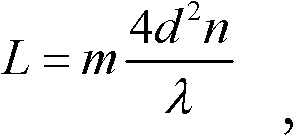
在一些实施例中,该处理器子系统包括控制器,其配置成发送控制信号到调制器,该调制器被配置成响应于控制信号而将接收的光脉冲部分单调地调制为时间的函数。在一些实施例中,该处理器子系统可以包括分立的现成组件。在一些实施例中,该处理器子系统包括控制器,其配置成发送控制信号到调制器,该调制器被配置成响应于控制信号而将接收的光脉冲部分单调地调制为时间的函数。在一些实施例中,该调制器具有是时间和电压的函数的响应函数,并且该系统存储了表征该调制器的响应函数的信息。一些实施例还包括补偿器,其被配置成增加该调制器的接收角。In some embodiments, the processor subsystem includes a controller configured to send a control signal to a modulator configured to monotonically modulate the portion of the received light pulse as a function of time in response to the control signal. In some embodiments, the processor subsystem may include discrete off-the-shelf components. In some embodiments, the processor subsystem includes a controller configured to send a control signal to a modulator configured to monotonically modulate the portion of the received light pulse as a function of time in response to the control signal. In some embodiments, the modulator has a response function that is a function of time and voltage, and the system stores information characterizing the response function of the modulator. Some embodiments also include a compensator configured to increase the acceptance angle of the modulator.
在一些实施例中,该用于生成的装置包括偏振分束器。在其它实施例中,该用于生成的装置包括棱镜。在一些实施例中,该用于生成的装置包括至少一个焦平面阵列,该焦平面阵列包括多个像素,每个像素具有100,000个或更多个电子的阱深。在一些实施例中,该用于生成的装置包括至少一个包括多个像素的焦平面阵列,并且还包括具有多个区域的滤波器,每个区域位于像素的前方,并且被配置成以预定方式衰减传送到该像素的光。在一些实施例中,该系统存储了表征滤波器的矩阵。In some embodiments, the means for generating includes a polarizing beam splitter. In other embodiments, the means for generating includes a prism. In some embodiments, the means for generating includes at least one focal plane array including a plurality of pixels each having a well depth of 100,000 electrons or more. In some embodiments, the means for generating includes at least one focal plane array including a plurality of pixels, and further includes a filter having a plurality of regions, each region positioned in front of a pixel and configured to Attenuates the light sent to this pixel. In some embodiments, the system stores matrices characterizing the filters.
在一些实施例中,该传感器子系统还包括宽频带或多频带(例如,可见)成像子系统,该成像子系统包括:图像传感器,其被配置成获得场景的宽频带或多频带图像;以及光学器件,其被配置成将接收的光的一部分引导到图像传感器。该处理器子系统可以被配置成将该三维图像与宽频带或多频带图像组合在一起以生成场景的图像。In some embodiments, the sensor subsystem further includes a broadband or multi-band (e.g., visible) imaging subsystem comprising: an image sensor configured to obtain a broadband or multi-band image of the scene; and Optics configured to direct a portion of the received light to the image sensor. The processor subsystem may be configured to combine the three-dimensional image with the broadband or multi-band image to generate an image of the scene.
在一些实施例中,第一和第二图像中的至少一个包含最大强度的区域,其中该用于生成的装置包括具有饱和极限的传感器阵列,并且其中该系统被配置成通过将光脉冲的能量增加到传感器阵列的饱和极限之上来增加三维图像的动态范围。In some embodiments, at least one of the first and second images contains a region of maximum intensity, wherein the means for generating comprises a sensor array having a saturation limit, and wherein the system is configured to pass the energy of the light pulse Increased above the saturation limit of the sensor array to increase the dynamic range of the 3D image.
在一些实施例中,该第一和第二图像中的至少一个包含最大强度的区域,该用于生成的部件包括具有饱和极限的传感器阵列,并且该处理器子系统被配置成:发送第一控制信号到照明子系统,该第一控制信号包括用于生成具有第一能量的光脉冲的指示,该第一能量被选择成使得该最大强度的区域处于传感器阵列的饱和极限的阈值百分比处或在该百分比之上,但是在饱和极限之下;并且获得基于具有该第一能量的光脉冲的反射或散射部分的第一三维图像。处理器子系统还可以被配置成:发送第二控制信号到照明子系统,该第二控制信号包括用于生成具有第二能量的光脉冲的指示,该第二能量被选择成使得最大强度的区域在传感器阵列的饱和极限之上;并且获得基于具有第二能量的光脉冲的反射或散射部分的第二三维图像。该处理器子系统还可以被配置成组合第一和第二三维图像,以获得与第一和第二三维图像相比具有增加的分辨率的第三三维图像。在一些实施例中,选择第二能量,使得最大强度的区域至少是该焦平面阵列的饱和极限的4倍。In some embodiments, at least one of the first and second images contains a region of maximum intensity, the means for generating includes a sensor array with a saturation limit, and the processor subsystem is configured to: send a first a control signal to the illumination subsystem, the first control signal including an indication for generating a light pulse having a first energy selected such that the region of maximum intensity is at a threshold percentage of the saturation limit of the sensor array or above the percentage, but below the saturation limit; and obtaining a first three-dimensional image based on the reflected or scattered portion of the light pulse having the first energy. The processor subsystem may also be configured to: send a second control signal to the lighting subsystem, the second control signal including an indication for generating light pulses having a second energy selected such that the maximum intensity the region is above the saturation limit of the sensor array; and a second three-dimensional image based on the reflected or scattered portion of the light pulse having the second energy is obtained. The processor subsystem may also be configured to combine the first and second three-dimensional images to obtain a third three-dimensional image having increased resolution compared to the first and second three-dimensional images. In some embodiments, the second energy is selected such that the region of maximum intensity is at least 4 times the saturation limit of the focal plane array.
在一些实施例中,该处理器子系统被配置成:指示该照明子系统发射多个光脉冲;调节调制器的时序,使得对于该多个光脉冲中的每个光脉冲,调制在不同时间开始;获得对应于该多个光脉冲中的每个光脉冲的多个三维图像;以及基于该多个三维图像获得增强的三维图像,该增强的三维图像对应于比该多个三维图像中的任一个的距离窗更大的距离窗。In some embodiments, the processor subsystem is configured to: instruct the illumination subsystem to emit a plurality of light pulses; adjust the timing of the modulator such that for each of the plurality of light pulses, modulation occurs at a different time start; obtaining a plurality of three-dimensional images corresponding to each light pulse in the plurality of light pulses; and obtaining an enhanced three-dimensional image based on the plurality of three-dimensional images, the enhanced three-dimensional image corresponding to Either distance window is greater than the distance window.
在一些实施例中,该处理器子系统被配置成:发送第一控制信号到照明子系统,该第一控制信号包括用于生成第一光脉冲的指示;发送第二控制信号到调制器,该第二控制信号包括用于在第一时间窗上调制该第一光脉冲的接收部分的指示;获得基于第一光脉冲的调制部分的第一三维图像;发送第三控制信号到照明子系统,该第三控制信号包括用于生成第二光脉冲的指示;发送第四控制信号到调制器,该第四控制信号包括用于在第二时间窗上调制该第二光脉冲的接收部分的指示;获得基于第二光脉冲的调制部分的第二三维图像;以及组合第一和第二三维图像,以获得与第一和第二三维图像相比具有增加的范围的第三三维图像。该第一和第二时间窗可以相互重叠。第一时间窗可以具有比第二时间窗更短的持续时间。第一时间窗可以具有与第二时间窗不同的开始时间。In some embodiments, the processor subsystem is configured to: send a first control signal to the lighting subsystem, the first control signal including an indication for generating the first light pulse; send a second control signal to the modulator, The second control signal includes an indication for modulating the received portion of the first light pulse over a first time window; obtaining a first three-dimensional image based on the modulated portion of the first light pulse; sending a third control signal to the lighting subsystem , the third control signal includes an indication for generating a second light pulse; a fourth control signal is sent to the modulator, the fourth control signal includes an instruction for modulating the receiving portion of the second light pulse over a second time window Instructing; obtaining a second three-dimensional image based on the modulated portion of the second light pulse; and combining the first and second three-dimensional images to obtain a third three-dimensional image having an increased range compared to the first and second three-dimensional images. The first and second time windows may overlap each other. The first time window may have a shorter duration than the second time window. The first time window may have a different start time than the second time window.
在一些实施例中,该三维图像具有亚厘米分辨率。In some embodiments, the three-dimensional image has sub-centimeter resolution.
根据本发明的另一方面,一种三维成像的方法,包括:发射具有发散度的光脉冲,该光脉冲足以照射具有宽视场的场景;在宽视场上接收由该场景反射或散射的光脉冲部分;用调制器将接收的光脉冲部分调制为时间的函数,以形成经过调制的所接收光脉冲部分;生成对应于该接收的光脉冲部分的第一图像;生成对应于经过调制的所接收光脉冲部分的第二图像;以及获得基于第一和第二图像的该场景的三维图像。According to another aspect of the present invention, a method for three-dimensional imaging includes: emitting light pulses with divergence sufficient to illuminate a scene with a wide field of view; receiving light reflected or scattered by the scene on the wide field of view the light pulse portion; modulating the received light pulse portion as a function of time with the modulator to form a modulated received light pulse portion; generating a first image corresponding to the received light pulse portion; generating a first image corresponding to the modulated a second image of the received light pulse portion; and obtaining a three-dimensional image of the scene based on the first and second images.
在一些实施例中,生成该第一图像包括将第二图像加入第三图像。在一些实施例中,用该调制器调制包括调制所接收光脉冲部分的偏振状态。In some embodiments, generating the first image includes adding the second image to the third image. In some embodiments, modulating with the modulator includes modulating a polarization state of the portion of the received light pulse.
根据本发明的另一方面,一种用于调制具有波长λ的光的偏振的调制器,该调制器包括:横向Pockels盒的堆叠,每个横向Pockels盒包括电光材料的板以及分别布置在该板的相对主表面上的第一和第二电极;与每个横向Pockels盒的第一电极电接触的第一导体;与每个横向Pockels盒的第二电极电接触的第二导体;以及与第一和第二电极电接触的电压源,每个横向Pockels盒的板具有近似等于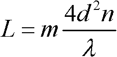
在一些实施例中,该电压源经由第一和第二导体在每个横向Pockels盒的第一和第二电极上施加小于100V的电压。在一些实施例中,该电压源经由第一和第二导体在每个横向Pockels盒的第一和第二电极上施加小于25V的电压。根据本发明的另一方面,从由磷酸二氢钾(KDP)、磷酸二氘钾(KD*P)、铌酸锂(LN)、周期性极化的铌酸锂、钽酸锂、磷酸钛氧铷(RTP)、偏硼酸钡(BBO)和它们同形体组成的组中选择电光材料。根据本发明的另一方面,该电光材料包括周期性极化的铌酸锂。在一些实施例中,该板具有小于100μm的厚度。在一些实施例中,第一和第二电极包括透明导体。在一些实施例中,波长在可见光范围。在一些实施例中,波长在近红外范围。在一些实施例中,波长在1400nm和2500nm之间。在一些实施例中,调制器具有至少40度的接收角。在一些实施例中,调制器具有至少5度的接收角。在一些实施例中,调制器具有至少1度的接收角。在一些实施例中,调制器还具有至少1英寸(例如,至少2英寸)的通光孔径。In some embodiments, the voltage source applies a voltage of less than 100 V across the first and second electrodes of each lateral Pockels cell via the first and second conductors. In some embodiments, the voltage source applies a voltage of less than 25V across the first and second electrodes of each lateral Pockels cell via the first and second conductors. According to another aspect of the present invention, from potassium dihydrogen phosphate (KDP), potassium diduterium phosphate (KD*P), lithium niobate (LN), periodically poled lithium niobate, lithium tantalate, titanium phosphate Electro-optic materials are selected from the group consisting of rubidium oxide (RTP), barium metaborate (BBO) and their isomorphs. According to another aspect of the invention, the electro-optic material comprises periodically poled lithium niobate. In some embodiments, the plate has a thickness of less than 100 μm. In some embodiments, the first and second electrodes include transparent conductors. In some embodiments, the wavelength is in the visible range. In some embodiments, the wavelength is in the near infrared range. In some embodiments, the wavelength is between 1400 nm and 2500 nm. In some embodiments, the modulator has an acceptance angle of at least 40 degrees. In some embodiments, the modulator has an acceptance angle of at least 5 degrees. In some embodiments, the modulator has an acceptance angle of at least 1 degree. In some embodiments, the modulator also has a clear aperture of at least 1 inch (eg, at least 2 inches).
根据本发明的另一方面,一种用于调制光的偏振的调制器,该调制器包括:横向Pockels盒的堆叠,每个横向Pockels盒包括电光材料的板以及分别布置在该板的相对主表面上的第一和第二电极;与每个横向Pockels盒的第一电极电接触的第一导体;与每个横向Pockels盒的第二电极电接触的第二导体;以及与第一和第二电极电接触的电压源,该第一和第二导体包括具有与电光材料具有的折射率近似相同的折射率的透明电极。According to another aspect of the present invention, a modulator for modulating the polarization of light comprises: a stack of transverse Pockels cells, each transverse Pockels cell comprising a plate of electro-optic material and opposite main First and second electrodes on the surface; a first conductor in electrical contact with the first electrode of each lateral Pockels cell; a second conductor in electrical contact with the second electrode of each lateral Pockels cell; A voltage source in electrical contact with two electrodes, the first and second conductors comprising transparent electrodes having a refractive index approximately the same as that of the electro-optic material.
附图说明 Description of drawings
图1图示根据本发明的一些实施例的用于获得场景的三维图像的系统的透视图。Figure 1 illustrates a perspective view of a system for obtaining a three-dimensional image of a scene according to some embodiments of the invention.
图2示意性图示从图1的场景反射的光脉冲部分的单调偏振调制。FIG. 2 schematically illustrates the monotonic polarization modulation of light pulse portions reflected from the scene of FIG. 1 .
图3示意性图示使用来自图2的经过调制的光脉冲部分形成的二维和三维图像。FIG. 3 schematically illustrates two-dimensional and three-dimensional images formed using the modulated light pulse portions from FIG. 2 .
图4图示根据本发明的一些实施例的获得场景的三维图像的方法的总览。Fig. 4 illustrates an overview of a method of obtaining a three-dimensional image of a scene according to some embodiments of the invention.
图5示意性图示根据本发明的一些实施例的图1的系统中的部件。Figure 5 schematically illustrates components in the system of Figure 1, according to some embodiments of the invention.
图6A图示根据本发明的一些实施例的用于生成具有小于1纳秒的持续时间的空间均匀的光脉冲的光源。Figure 6A illustrates a light source for generating spatially uniform light pulses with a duration of less than 1 nanosecond, according to some embodiments of the invention.
图6B-6C示意性图示根据本发明的一个实施例的图6A的光源的空间和时间模式结构。Figures 6B-6C schematically illustrate the spatial and temporal pattern structure of the light source of Figure 6A, according to one embodiment of the present invention.
图7A图示根据本发明的一些实施例的宽孔径、低电压Pockels组件的透视图。Figure 7A illustrates a perspective view of a wide aperture, low voltage Pockels assembly according to some embodiments of the invention.
图7B图示根据本发明的一些实施例的替代性的宽孔径、低电压Pockels组件的透视图。Figure 7B illustrates a perspective view of an alternative wide aperture, low voltage Pockels assembly according to some embodiments of the invention.
图7C图示根据本发明的一些实施例的替代性的宽孔径、低电压Pockels组件的透视图。Figure 7C illustrates a perspective view of an alternative wide aperture, low voltage Pockels assembly according to some embodiments of the invention.
图8图示根据本发明的一些实施例的用于增加三维图像的信息内容的方法中的各步骤。Fig. 8 illustrates steps in a method for increasing the information content of a three-dimensional image according to some embodiments of the invention.
图9A示意性图示根据本发明的一些实施例的滤色镜,其可以用于增加在三维成像系统中使用的焦平面阵列的动态范围。Figure 9A schematically illustrates a color filter according to some embodiments of the present invention that may be used to increase the dynamic range of a focal plane array used in a three-dimensional imaging system.
图9B图示根据本发明的一些实施例的可买到的滤色镜的传输光谱,该滤色镜可以用于增加焦平面阵列的动态范围。Figure 9B illustrates the transmission spectrum of a commercially available color filter that can be used to increase the dynamic range of a focal plane array, according to some embodiments of the invention.
图10图示根据本发明的一些实施例的扩展三维图像的范围的方法中的各步骤。FIG. 10 illustrates steps in a method of extending the range of a three-dimensional image according to some embodiments of the invention.
图11示意性图示根据本发明的一些实施例的三维成像系统的替代性实施例。Figure 11 schematically illustrates an alternative embodiment of a three-dimensional imaging system according to some embodiments of the invention.
图12示意性图示根据本发明的一些实施例的三维成像系统的替代性实施例。Figure 12 schematically illustrates an alternative embodiment of a three-dimensional imaging system according to some embodiments of the invention.
具体实施方式 Detailed ways
1.概述1 Overview
本发明的实施例提供了用于获得场景(包括宽视场场景)的高分辨率图像的系统和方法。具体地,该系统和方法可以用高的空间和距离分辨率同时记录场景中多个对象的三维位置信息,以及关于场景的强度(灰度级或色彩)信息。对于每个图像,为像素阵列中的每个像素记录了该信息(坐标和强度两者)。该强度和位置信息被组合为与人对场景的视觉近似的单个三维图像,并且该单个三维图像还记录场景中每个对象的形状和相对位置的三维坐标。可以以与数字摄像机类似的方式获取一系列这样的图像,提供场景中随着时间改变的“影片(movie)”,该影片中的每个三维图像称为帧。在许多情况下,该被成像的场景可以包括处于距系统多种距离的许多对象。本发明的系统记录了对应于每个像素元件的对象的部分的三维坐标和强度,从而相对于三维成像设备以及由三维成像设备记录的图像中该场景的其它部分,提供了场景中每个个体对象的三维形状以及总体坐标。如果希望获得参照物的绝对帧,则可以包括GPS单元或用于确定成像系统的绝对位置的其它适当的装置。Embodiments of the present invention provide systems and methods for obtaining high-resolution images of scenes, including wide-field-of-view scenes. Specifically, the system and method can simultaneously record three-dimensional position information of multiple objects in a scene, as well as intensity (grayscale or color) information about the scene, with high spatial and distance resolution. For each image, this information (both coordinates and intensities) is recorded for each pixel in the pixel array. This intensity and position information is combined into a single 3D image that approximates a human's vision of the scene, and this single 3D image also records the 3D coordinates of the shape and relative position of each object in the scene. A series of such images can be acquired in a similar manner to a digital camera, providing a "movie" of changes in the scene over time, each three-dimensional image in the movie being called a frame. In many cases, the imaged scene may include many objects at various distances from the system. The system of the present invention records the three-dimensional coordinates and intensities of the part of the object corresponding to each pixel element, thereby providing a complete picture of the intensity of each individual in the scene relative to the three-dimensional imaging device and other parts of the scene in the image recorded by the three-dimensional imaging device. The three-dimensional shape of the object and its overall coordinates. If an absolute frame of the reference object is desired, a GPS unit or other suitable means for determining the absolute position of the imaging system may be included.
本发明的一个方面提供了记录多种场景的三维信息和彩色或单色图像的能力,其中特别关注包括接近的对象的那些场景。对于短距离成像应用(例如,对象比1km更接近),观察在大的空间区域上分布的对象通常是有用的。这转化为对于宽视场(FOV)的需要。在本发明的环境中,“宽视场”指朝向一度或更大角度的视场。视场典型地表达为场景的侧边之间的角度间隔。对于在本文中描述的系统和方法的一些使用,大于1度或大于5度或大于10度的FOV是有用的,因为它们可以例如通过提供关于对象的环境的信息来增加场景的信息内容。之前已知的系统已经不能实现这样的宽FOV。One aspect of the invention provides the ability to record three-dimensional information and color or monochrome images of a variety of scenes, with particular focus on those scenes that include close objects. For short-range imaging applications (eg, objects closer together than 1 km), it is often useful to observe objects distributed over a large spatial region. This translates into a need for a wide field of view (FOV). In the context of the present invention, "wide field of view" refers to a field of view towards an angle of one degree or more. Field of view is typically expressed as the angular separation between sides of a scene. For some uses of the systems and methods described herein, FOVs greater than 1 degree, or greater than 5 degrees, or greater than 10 degrees are useful because they can increase the information content of a scene, for example, by providing information about an object's environment. Previously known systems have not been able to achieve such a wide FOV.
例如,Taboada描述了用于成像单个、远距离目标和单调偏振斜坡(monotonic polarization ramp)的三维坐标的技术。这将从目标返回的光脉冲的时间特征映射到可以通过一对摄像机容易地测量的特性强度范围上。尽管该简单技术足以获得关于远距离对象的一些深度信息,但是可以对其进行若干改进。本发明的实施例在由Taboada描述的基础上提供了若干改进方面。这些方面可能是重要的,因为发明的系统和方法可以用于记录关于场景中的若干对象的三维信息,具体地是因为距系统和对象的距离变得更短。这些实施例可以采用这些改进方面的任一个或其任何组合,包括提供高的动态范围、自适应景深、宽视场、高分辨率、帧到帧配准以及其它。For example, Taboada describes a technique for imaging the three-dimensional coordinates of a single, distant target and a monotonic polarization ramp. This maps the temporal signature of light pulses returning from the target onto a characteristic intensity range that can be easily measured by a pair of cameras. Although this simple technique is sufficient to obtain some depth information about distant objects, several improvements can be made to it. Embodiments of the present invention provide several improvements over those described by Taboada. These aspects may be important because the inventive system and method can be used to record three-dimensional information about several objects in a scene, in particular because the distances to the system and objects become shorter. Embodiments may employ any or any combination of these improvements, including providing high dynamic range, adaptive depth of field, wide field of view, high resolution, frame-to-frame registration, and others.
图1图示根据本发明的一些实施例的用于获得场景190的三维、宽FOV图像的系统100的透视图。以下在题为“方法”的部分中提供了使用诸如系统100的系统获得场景的三维图像的方法的更多细节,并且以下在题为“系统”的部分中提供了诸如系统100的系统的部件的更多细节。尽管结合笛卡尔坐标系描述了图示的实施例,但是可以使用其它坐标系。Figure 1 illustrates a perspective view of a
如图1所示,系统100包括照明子系统110、传感器子系统120、处理子系统140和其中安装了各种子系统的主体150。主体150还可以包括保护罩(未示出)。系统100的具体形式可以根据希望的性能参数和期望的应用而不同。例如,如果希望将系统100用于家用,则它优选地是足够小和轻的,以便类似于便携式摄像机地由单手持有,并且可以被配置成以适中的分辨率记录相对接近的场景。或者,如果希望将系统100用于调查建筑工地,则它可以被配置成以高分辨率成像大和/或远的场景,并且系统的尺寸将是次要的考虑因素。As shown in FIG. 1,
照明子系统110包括图1中未示出但是以下被更详细地描述的光源和发送透镜(transmission lens)112,该发送透镜112可以包括单个透镜、复合透镜或透镜的组合。该光源被配置成生成光脉冲119,取决于z方向上的希望的分辨率,该光脉冲优选地具有2纳秒或更小的持续时间,例如,1纳秒和50皮秒之间的持续时间。发送透镜112被配置成将脉冲119的发散度增加到1度或更大的角度
传感器子系统120包括大孔径接收透镜121,其收集反射的脉冲部分127、128、129。该适当的孔径尺寸将取决于具体应用,并且可以是例如小于1cm和2.5cm之间。该反射脉冲的其它部分(例如,在不同于回到系统100的方向上反射的、由点划线图示的那些部分)可能不会被接收光学器件121捕获。至于发射透镜112,接收透镜121可以包括单个透镜、复合透镜或透镜的组合或其它反射或折射元件。接收光学器件121还可以收集关于场景190的宽频带或多频带(例如,可见)信息,例如,场景190散射或反射向接收光学器件121的环境光。这样,对于这种情况,接收透镜121优选地被配置成减少或消除光学系统设计的领域中已知的可能像差,该像差可能会相对于接收的一个或多个频带劣化图像质量。或者,可以提供独立的接收透镜来接收宽频带或多频带光。如以下详细描述的,传感器子系统可以包括独立的可见光成像子系统,其基于从场景收集的可见光而记录场景190的彩色或灰度级图像。稍后这样的图像被与关于场景的位置和形状信息相组合。The
传感器子系统120基于接收透镜121收集的脉冲部分127、128、129创建多个图像。这些图像包含关于场景190中的对象191、192的位置信息。为了创建这样的图像,传感器子系统例如使用以下更详细描述的宽视场Pockels组件来将进入脉冲部分127、128、129的偏振状态改变为时间的函数。当跟随有分析器(例如,放置在Pockels盒之后的偏振元件)时,通过分析器的相应传输作为时间的函数而变化。例如,如图2所示,传感器子系统120可以在50到100纳秒的时间之间(其中0纳秒对应于生成该光脉冲的时刻)将由接收透镜121收集的、通过光的分析器的传输200从零变为一。这样,因为行进不同距离到达和远离场景190中的对象而在时间上相对于彼此延迟的脉冲部分127、128、129经历程度各不相同的传输。具体地,相对于脉冲部分128,脉冲部分129从对象191的更近部分反射,所以经历比脉冲部分128更少的传输。脉冲部分127从更远的对象192反射,所以经历比脉冲部分128更多的传输。这样,传感器子系统120调制脉冲部分的传输,将该脉冲部分的TOF编码在由该FPA接收的强度上,且从而编码了该脉冲部分行进到和离开场景中的对象的具体特征的距离。The
传感器子系统120通过使用诸如棱镜或偏振分束器的光学元件来将每个脉冲分为它的正交偏振分量(例如,H-和V-偏振分量),然后记录该两个偏振分量的互补图像,而确定每个脉冲部分127、128、129的偏振的程度。例如,如图3所示,第一图像201分别以强度区域227、228、229的形式包含关于脉冲部分127、128、129的H偏振分量的信息。第二图像201’分别以强度区域227’、228’、229’的形式包含关于脉冲部分127、128、129的V偏振分量的信息。图像201中的强度区域229显著地比图像201’中的强度区域229’更暗,因为如图2所示,脉冲部分129相对较早到达,并且经历了相对少的偏振调制。相反,图像201中的强度区域227显著比图像201’中的强度区域227’更暗,因为脉冲部分127相对较晚到达,并且经历了显著的偏振调制。强度区域228和228’为大约相同的强度,因为脉冲部分128通过该偏振的调制200到达大约中途之处,并且从而包含大约相等数量的正交偏振分量(例如,H和V)。The
图1所示的处理器子系统140可以存储图像201、201’,并且进一步执行用于获得场景190中的对象191、192的距离和形状信息的处理。例如,如以下更详细所述的,处理器子系统140可以规格化图像201、201’,以便补偿对象191、192之间反射或散射方面的变化。处理器子系统140然后可以基于规格化图像(形成图3所示的三维图像300)计算场景190中不同对象的位置和形状,这形成了图3中所示的三维图像300,其包括关于对象191、192的距离信息。图像300包括分别对应于脉冲部分127、128、129的对象区域327、328、329,并且包括关于对象191和192的位置和形状信息。此外,处理器子系统140可以将计算的距离信息与白光图像组合,以提供包括关于场景的灰度级或色彩信息的场景190的三维图像,从而模拟了人对于该场景的视觉。如以下进一步详细描述的,处理器子系统140还可以控制和协调照明子系统110和传感器子系统120的操作。Processor subsystem 140 shown in FIG. 1 may store
在一个说明性实施例中,系统100具有在20米的距离处大约1mm的距离分辨率,以及在100米的距离处大约3mm或更小的距离分辨率。数据获取速率可以是例如在每秒3000万到10亿点之间,这明显地快于使用基于扫描的设备可能取得的数据获取速率。在30到45度的视场的情况下,角度分辨率可以是例如大约0.02度。该设备可以是“面包盒”或更小的尺寸,或者甚至在一些实施例中是“咖啡杯”或更小的尺寸,其具有小于约10000美元或者甚至小于1000美元的成本。In one illustrative embodiment,
尽管系统100在一些方面类似于Taboada所公开的,但是它在许多重大的方面存在不同。首先,Taboada没有记载他的系统的动态范围、距离分辨率和光学分辨率,而这对于实现商业上可行的成像系统,特别是设计成收集关于可能位于场景内的不同距离处的多个对象的信息的系统是重要的。相比之下,如在本文中更详细描述的,系统100可以被配置成通过例如使用多种技术中的任何一种或全部来扩展系统的动态范围,而获得场景的任何方面的任何希望的分辨率的图像。此外,Taboada的系统通常表现为限于获取单个远程对象的长距离图像(如可以从飞机观看的图像)。例如,Taboada公开了使用之前已知的Kerrh盒或Pockels盒来调制反射光的偏振(具体是被安排成相互光串联并且电并联的Pockels盒的排列)。之前已知的Pockels盒可能要求无论何处的从几千到几万伏的电压,具有小的孔径(例如,1cm或更小),并且具有低的接收角(例如,1度的小的分数)。虽然其要求较低的电压,但是Taboada的所公开的光串联并且电并联的Pockels盒的排列将进一步减小通光孔径和接收角。从而,Taboada的系统将不能够使用从Pockels盒的表面法线偏离超过1度的某一小分数的光获得精确的距离信息,更不必说使用偏离该法线5度或更大角度的光。相比之下,如以下更详细描述的,系统100包括调制器,其使得能够使用偏离5到50度的光、从分布在整个宽视场中的对象散射的光来获取高分辨率距离信息,并且可能仅需要低得多的电压(例如,约几十伏或甚至小于十伏的电压)。Although
首先,将提供用于获得场景的三维图像的方法的概述。然后,将详细描述用于获得三维图像的系统。然后,将描述三维成像的各种潜在应用。最后,将描述其他实施例的一些实例。所描述的方法、系统、应用和实施例仅为示例性的,而非限制性的。First, an overview of a method for obtaining a three-dimensional image of a scene will be provided. Then, a system for obtaining a three-dimensional image will be described in detail. Then, various potential applications of 3D imaging will be described. Finally, some examples of other embodiments will be described. The methods, systems, applications, and embodiments described are exemplary only, and not limiting.
2.方法2. Method
现在将结合图4描述根据本发明的各个实施例(例如,系统100)的用于获得三维图像的方法。A method for obtaining a three-dimensional image according to various embodiments of the present invention (eg, system 100 ) will now be described with reference to FIG. 4 .
图4所示的方法400包括生成具有例如小于2纳秒的持续时间和宽视场的光脉冲(410),之后用这样的脉冲照射场景(420)。例如,可以通过本文中描述的照明子系统之一或任何其它合适的光脉冲发生器来生成这样的光脉冲。The
优选地,该光脉冲是空间均匀的。“空间均匀”意味着光脉冲的空间强度(在x-y平面中)在光束的大部分空间轮廓上的变化小于大约50%、或者小于40%、或者小于30%、或者小于20%、或者小于10%、或者小于5%、或者小于2%。例如,可以将该脉冲表征为具有“半高全宽(FWHM)”,其是通过识别该光束的最大强度并且识别具有该强度的一半或更大的光束的空间范围来确定的。在一些实施例中,脉冲的空间强度在由FWHM表征的空间区域上变化小于50%、或者小于40%、或者小于30%、或者小于20%、或者小于10%、或者小于5%、或者小于2%。在其它实施例中,空间强度轮廓的变化可以大于50%,或者甚至100%。如以下更详细描述的,在一些实施例中,可以用具有大量空间模式(例如,大于20个空间模式)的脉冲激光器生成这样的空间均匀的光脉冲。Preferably, the light pulses are spatially uniform. "Spatially uniform" means that the spatial intensity of the light pulse (in the x-y plane) varies by less than about 50%, or less than 40%, or less than 30%, or less than 20%, or less than 10% over most of the beam's spatial profile %, or less than 5%, or less than 2%. For example, the pulse can be characterized as having a "full width at half maximum (FWHM)" determined by identifying the maximum intensity of the beam and identifying the spatial extent of the beam having half that intensity or greater. In some embodiments, the spatial intensity of the pulse varies by less than 50%, or less than 40%, or less than 30%, or less than 20%, or less than 10%, or less than 5%, or less than 2%. In other embodiments, the variation of the spatial intensity profile may be greater than 50%, or even 100%. As described in more detail below, in some embodiments, such spatially uniform light pulses may be generated with a pulsed laser having a large number of spatial modes (eg, greater than 20 spatial modes).
由这样的激光器生成的脉冲的时间轮廓也可以是基本平滑的,这意味着作为时间的函数的该脉冲的强度平滑地变化。如以下更详细地描述的,在一些实施例中,可以用具有大量时间模式(例如,大于20个时间模式)的脉冲激光器生成这样的时间均匀光脉冲。The temporal profile of a pulse generated by such a laser may also be substantially smooth, meaning that the intensity of the pulse varies smoothly as a function of time. As described in more detail below, in some embodiments such temporally uniform light pulses may be generated with a pulsed laser having a large number of temporal modes (eg, greater than 20 temporal modes).
可以在电磁光谱的任何合适的部分内(例如,在光谱的可见光部分(400nm-700nm)中、或者在光谱的近红外部分(700nm-2500nm)中、或者在电磁光谱中的另一范围中)生成光脉冲。优选地,激光的脉冲能量足够高,以便提供可接受的信号量来表征感兴趣的场景,而同时也足够低,以对于系统的用户和场景的任何占据者的眼睛而言是安全的,且不需要特殊的预防。例如,与可见光波长相比,大于1400nm(例如,在1400nm和2500nm之间)的波长可以提供约为最大允许曝光限制的一千倍的增加,这意味着,与使用具有可见光波段中的波长的脉冲的情形相比,在使用具有大于1400nm波长的脉冲的情况下,可以用一千倍于之前的能量安全地照射该场景。实现眼睛安全的其它方式包括管理控制、高发散度和低的空间相干性。can be in any suitable part of the electromagnetic spectrum (for example, in the visible part of the spectrum (400nm-700nm), or in the near-infrared part of the spectrum (700nm-2500nm), or in another range in the electromagnetic spectrum) Generate light pulses. Preferably, the pulse energy of the laser is high enough to provide an acceptable amount of signal to characterize the scene of interest, while low enough to be safe for the eyes of the user of the system and any occupants of the scene, and No special precautions are required. For example, wavelengths greater than 1400 nm (e.g., between 1400 nm and 2500 nm) can provide approximately a thousand-fold increase in the maximum allowable exposure limit compared to visible light wavelengths, which means that compared to using Using pulses with a wavelength greater than 1400 nm, the scene can be safely illuminated with a thousand times more energy than in the case of pulses. Other ways to achieve eye safety include administrative control, high divergence, and low spatial coherence.
应当理解,可以基于具体应用来选择光脉冲的持续时间和发散度。例如,1纳秒脉冲可以用于实现0.01米的距离分辨率,而100皮秒脉冲可以用于实现0.001米的距离分辨率。在各个实施例中,取决于希望的距离分辨率,光脉冲的持续时间可以是例如1纳秒和10皮秒之间、或者500皮秒和50皮秒之间、或者200皮秒和100皮秒之间、或者100皮秒和10皮秒之间。此外,所希望的用于在特定距离成像的视场越宽,则可以选择的发散度(图1中的角度
方法400包括用大孔径透镜收集由场景反射和散射的光脉冲的各部分(430)。如上所述,这些光脉冲部分携带了关于场景的若干类型的信息。例如,尽管用单个脉冲照射该场景,但是取决于场景中不同对象或者对象的不同部分的相对位置和形状,接收透镜接收具有各种TOF的脉冲部分。
方法400也包括将收集的光脉冲部分的偏振调制为时间的函数(440)。这样的调制例如可以是时间的单调函数,如图2所示。在这样的实施例中,具有较短TOF的脉冲将比具有较长TOF的脉冲经历较少的偏振调制,使得能够容易地获得距离信息。然而,如以下更详细描述的,这样的调制不必是单调的。此外,可以调制收集的光脉冲部分的强度而非其偏振。
对其中偏振被调制为时间的单调函数的实施例而言,可以从场景的特定图像中获得的距离信息至少部分地基于该调制的持续时间。例如,再次参考图2,在50纳秒处开始,传输在50纳秒的跨度上从0变为1。这样,仅在该50纳秒调制窗(对应于7.5米的距离窗)期间到达的脉冲部分才将经历0和1之间的传输。从比7.5米更接近的对象反射并且因此在该调制窗于50纳秒处开始之前到达的脉冲部分,或者从比30米更远的对象反射并且因此在该调制窗已经关闭之后到达的脉冲部分,将具有更长或更短的TOF,所以将不会被图2中的具体波形调制。为了访问其它距离窗,偏振调制的开始时间和/或持续时间可以适当地变化。在一个实施例中,使用多种用于偏振调制的持续时间和/或开始时间重复方法400,并且组合得到的图像以形成具有比使用单个偏振调制可能获得的距离信息大得多的距离信息的三维图像。For embodiments where the polarization is modulated as a monotonic function of time, the distance information that can be obtained from a particular image of the scene is based at least in part on the duration of the modulation. For example, referring again to FIG. 2, starting at 50 nanoseconds, the transmission changes from 0 to 1 over a span of 50 nanoseconds. In this way, only the portion of the pulse arriving during this 50 nanosecond modulation window (corresponding to a range window of 7.5 meters) will undergo transmission between 0 and 1. The portion of the pulse that reflects from an object closer than 7.5 meters and therefore arrives before the modulation window starts at 50 nanoseconds, or reflects from an object further away than 30 meters and thus arrives after the modulation window has closed , will have a longer or shorter TOF, so will not be modulated by the specific waveform in Figure 2. In order to access other range windows, the start time and/or duration of the polarization modulation may be varied appropriately. In one embodiment, multiple durations and/or start times for polarization modulation are used to repeat the
方法400也包括获得调制的光脉冲部分的正交偏振分量(例如,H-和V-偏振分量,或者左和右圆偏振分量)的互补图像(450)。在一个实施例中,通过使用偏振分束器将这些脉冲部分分成它们的正交分量,并且将这些正交分量成像在各个焦平面阵列(FPA)上,获得这样的图像。FPA可以适于在或接近在步骤410处生成的光脉冲的中心波长处具有高灵敏度。在光脉冲处于可见光波段(例如,400到700nm)的情况下,基于可买到的CCD或CMOS的阵列可能是适合的,而如果光脉冲处于近红外波段(例如,700nm到2500nm),则可能要求其它阵列技术或材料。
方法400也包括将来自步骤450的互补图像规格化和组合,以便获得场景中对象的距离和形状信息(460)。如以下更详细描述的,可以逐像素进行这样的处理。
经由这样的方法或通过被配置成实现这样的方法的系统(例如,以下结合图5讨论的系统500)可获得的距离分辨率可以部分基于调制波形的长度,以及在测量该波形的辐照度和时序方面涉及的不确定性。辐照度测量中的不确定性与信噪比(SNR)有关。对于诸如由Taboada公开的长距离应用,从目标接收的光子数因为长距离而受限,这是因为信号按1/R2衰减,其中R是到目标的距离。则主导噪声项与暗电流、读出噪声和背景光(例如阳光)有关。对于这样的应用,使用非常低噪声的成像阵列可能是关键的。相比之下,根据当前发明的各种实施例,运行在近得多的距离上意味着设计照明子系统(例如,激光器)来提供足够的照明辐照度以提供高的SNR是实际的。对于这样的运行模式,主导的噪声项可能是返回信号的散粒噪声,其为接收信号的平方根。然后可以将该焦平面阵列选择为具有高动态范围的一个焦平面阵列(其可以用可以测量的最大信号除以该阵列的本征噪声级来定义)。因为散粒噪声级而非本征噪声水平是限制项,该焦平面阵列的一个有用的特征可以包括深阱(对应于高饱和水平)的存在。例如,100000电子或更大的阱深可以提供大约300或更大的SNR,只要本征噪声级为大约100个电子或更小。此外,尽管诸如由Taboada公开的应用可能要求配置焦平面阵列来最小化本征噪声,这样的阵列可能要求限制像素的数目或增加成本的具体设计,这可能降低了系统的实际性能。The distance resolution achievable via such an approach or by a system configured to implement such an approach (e.g.,
系统system
图5示意性图示根据本发明的一些实施例的三维成像系统500中的选定的部件。应该理解,可以用其他光学配置(如以下所述的)来替代性地提供系统500的功能。如图5所示,系统500包括照明子系统510、传感器子系统520和处理器子系统540。现在将详细描述这些子系统中的每一个。FIG. 5 schematically illustrates selected components of a three-
A.照明子系统510
照明子系统510包括用于生成光脉冲的光源511、用于控制生成的光脉冲的发散度的发送(Tx)透镜512、以及用于增强光脉冲的空间轮廓的可选相位板或其它光束整形元件513。或者,可以颠倒该透镜512和该可选的相位板513的位置。也可以将这些元件组合在单个光学器件或一套光学器件中。照明子系统510可以与控制器541通信,而后者可以控制和/或监视来自光源511的光脉冲的发射,并且还可以控制和/或监视发送透镜512给予生成的光脉冲的发散度。The
如上所述,参见图1,照明子系统优选地生成具有平滑的空间轮廓、平滑的时间轮廓和例如5和40之间的发散度的光脉冲。该光脉冲可以处于电磁光谱的任何合适部分,例如,处于可见光波段(例如,400-700nm)或处于近红外波段(例如,700nm-2500nm)。通常,认为在近红外波段的特定区域中生成的脉冲比可见光波段中的相当功率的脉冲对眼睛更安全。光源511被配置成在希望的电磁波段中生成光脉冲,并且透镜512和可选的相位板513被配置成提供具有希望的发散度的光脉冲,并且可选地进一步增强该脉冲的光学轮廓。在一些实施例中,光源511是产生具有至少5μJ能量、或者至少100μJ能量、或者至少1mJ能量、或者至少10mJ能量的光脉冲的激光器。因为该激光束的高发散度,这样的激光能量对眼睛可能是相对安全的。As mentioned above, referring to FIG. 1 , the illumination subsystem preferably generates light pulses with a smooth spatial profile, a smooth temporal profile, and a divergence of between 5 and 40, for example. The light pulses may be in any suitable part of the electromagnetic spectrum, eg, in the visible band (eg, 400-700nm) or in the near-infrared band (eg, 700nm-2500nm). In general, pulses generated in a specific region of the near-infrared band are considered safer for the eyes than pulses of comparable power in the visible band.
首先,将提供与之前已知的激光器相关联的一些事项的简要描述。然后,将提供可以用作光源511的低相干性激光器的描述。First, a brief description of some matters associated with previously known lasers will be provided. Then, a description will be provided of a low-coherence laser that can be used as the
激光脉冲的独特特征之一是它被聚焦为小直径并且(与之有关地)传播长距离而不会明显地改变直径的能力。自1960年代早期激光器的发明以来,已经进行大量的工作来在这些方面改进激光器设备的性能(特别是能够将激光聚焦到衍射极限)。一些这样的努力集中在例如通过仔细地设计激光腔以限制激光器的空间和时间模式的数目、提供最佳曲率的腔镜、通过在激光腔内的特定位置处设置小的孔径以抑制较高阶模式的激光发射、和/或控制诸如热透镜效应的引起像差的效应,来增加激光束的空间和时间相干性。其它设备和技术也可以用于改进光束特性。One of the unique features of a laser pulse is its ability to be focused to a small diameter and (related thereto) to travel long distances without appreciably changing diameter. Since the invention of the early laser in the 1960s, a great deal of work has been done to improve the performance of laser devices in these respects (especially the ability to focus the laser light to the diffraction limit). Some such efforts have focused, for example, on limiting the number of spatial and temporal modes of the laser by carefully designing the laser cavity, providing cavity mirrors with optimal curvature, and suppressing higher-order Pattern laser emission, and/or control aberration-inducing effects such as thermal lensing, to increase the spatial and temporal coherence of the laser beam. Other devices and techniques can also be used to improve beam characteristics.
用于提高主要以基模输出能量的激光器的效率的技术是将增益体积(gainvolume)的直径与激光腔的模体积的直径匹配。模直径由腔镜的曲率半径和这些镜的间距确定。对于稳定谐振腔,该直径典型地是小的。因为增益饱和效应的缘故,这限制了可以从每个脉冲的激光提取的总能量。不稳定谐振器设计可以用于增加基础空间模式的腔内模式尺寸,使得可以使用更大的增益体积,同时仍仅仅激发基础空间模式。然而,要求高增益激光器介质来克服不稳定腔中固有的高损失,并且源自腔镜的衍射效应引起了输出空间轮廓的显著的调制。在激光腔外部,可以使用可变形镜和相位校正器来校正可能降低激光束的聚焦能力的像差。A technique for increasing the efficiency of lasers that output energy primarily in the fundamental mode is to match the diameter of the gain volume to the diameter of the mode volume of the laser cavity. The mode diameter is determined by the radius of curvature of the cavity mirrors and the spacing of these mirrors. For a stable resonant cavity, this diameter is typically small. This limits the total energy that can be extracted from each pulse of laser light due to gain saturation effects. Unstable resonator designs can be used to increase the intracavity mode size of the fundamental spatial mode, allowing a larger gain volume to be used while still only exciting the fundamental spatial mode. However, high-gain laser media are required to overcome the high losses inherent in unstable cavities, and diffraction effects originating from the cavity mirrors cause significant modulation of the output spatial profile. Outside the laser cavity, deformable mirrors and phase correctors can be used to correct aberrations that may reduce the focusing ability of the laser beam.
激光器设计中这类技术的使用可能导致激光器设备的其它特性方面的牺牲。例如,在试图减小热失真的影响、增益饱和效应、更高阶横向模式的影响等期间,可能减小设计输出功率或能量。用于改进光束的空间相干性(例如,用于消除更高阶模式)的设计选择还可能导致使用更昂贵的镜和光学设计。这样的设计考虑可能增加了系统的成本和复杂性。The use of such techniques in laser design may result in sacrifices in other properties of the laser device. For example, the design output power or energy may be reduced during an attempt to reduce the effects of thermal distortion, gain saturation effects, effects of higher order transverse modes, etc. Design choices to improve the spatial coherence of the beam (eg, to eliminate higher order modes) may also result in the use of more expensive mirrors and optical designs. Such design considerations may add cost and complexity to the system.
然而,在诸如激光成像的领域存在许多应用,其中激光束的聚焦能力不重要。实际上,可以引入额外的光学元件以扩展激光束来填充感兴趣的区域。在这样的应用中,激光束的空间和时间相干性可能导致“斑点(speckle)”,在其中激光束与自身发生干涉,这导致了目标上的激光点上的不希望的强度变化。对于一些激光成像应用,可能希望减少激光束的空间和时间相干性,使得激光主要用作单色的、控制良好的、均匀的“闪光”。用于产生配置成用于这样的低相干性应用的激光的标准可能显著地不同于那些用于衍射受限光束的标准。例如,低相干性激光可能被配置成以相对低的成本为脉冲和连续波(CW)激光设备提供高输出功率或能量。较低的空间相干性也可以减小激光在眼睛的视网膜上的聚焦能力,从而提高了对眼睛的安全性。However, there are many applications in fields such as laser imaging where the focusing ability of the laser beam is not important. In fact, additional optics can be introduced to expand the laser beam to fill the region of interest. In such applications, the spatial and temporal coherence of the laser beam can lead to "speckles" where the laser beam interferes with itself, which results in undesired intensity variations at the laser spot on the target. For some laser imaging applications, it may be desirable to reduce the spatial and temporal coherence of the laser beam so that the laser acts primarily as a monochromatic, well-controlled, uniform "flare". The standards used to generate laser light configured for such low-coherence applications may differ significantly from those used for diffraction-limited beams. For example, low coherence lasers may be configured to provide high output power or energy for pulsed and continuous wave (CW) laser devices at relatively low cost. Lower spatial coherence also reduces the laser's ability to focus on the eye's retina, increasing eye safety.
再次参见图5,三维成像系统是宽视场系统的一个非限制性例子,其中减小的空间和/或时间相干性可能是有用的。照明子系统510可以生成具有大的发散度(例如,在1和180之间、或者1和90之间、或者1和40之间、或者2和40之间、或者5和40度的发散度之间)和低的空间和/或时间相干性的激光脉冲,而衍射受限的激光可能具有一度的仅仅一小部分的发散度和大量的空间和时间相干性。大的发散度和缺少空间和/或时间相干性可能减少在用该激光束照射的对象的表面处的激光辐照度的强度波动量。由照明子系统510生成的激光束的更为平滑的强度轮廓可以提高传感器子系统520的性能。Referring again to FIG. 5, a three-dimensional imaging system is a non-limiting example of a wide field of view system where reduced spatial and/or temporal coherence may be useful. The
图6A示意性图示适于用作图5的光源511的低相干性激光器600的一个实施例。激光器600包括生成光脉冲的种子激光器610,并且可选地还包括放大器620,其可以包括用于放大由种子激光器610生成的激光脉冲的强度的一级或多级。激光器600可以在图5所示的控制器541的控制下运行。应该注意,激光器600也可以是独立系统(也就是说,不包括在系统500中),在这种情况下它可以包括它自身的激光控制器。FIG. 6A schematically illustrates one embodiment of a low-
参见图6A,种子激光器610包括增益介质631、第一和第二腔镜623、633、二极管或其它泵浦634、可选的Q开关635和可选的偏振器636。腔镜633优选地是高反射镜,而腔镜623是部分透射性的,以允许激光从激光器输出并且进入可选的放大器620或到达场景。腔镜632、633中的至少一个可选地可以直接覆盖在增益介质631上,这消除了对于独立的光学部件的需要。有源Q开关635和偏振器636可以被配置成拖延腔内的激光发射,直到希望的时间为止(例如,直到希望从种子激光器610获得激光脉冲的时间为止)。尽管在本文中描述的许多实施例涉及种子激光器610被配置成生成激光脉冲,种子激光器610也可以被配置成生成连续波(CW)激光束。Referring to FIG. 6A ,
在一些实施例中,种子激光器610优选地生成1纳秒或更短的激光脉冲,并且包括足够数目的空间模式来提供基本均匀的空间轮廓。上面给出了“基本均匀的”时间和空间模式的含义。此外,许多空间模式的存在也可以增加激光束中存在的纵向模式的总数。例如,如图6B-6C所示,由种子激光器610生成的激光脉冲优选地包括足够数目的空间模式651、…659,当这样的空间模式可能相互干涉时,结果是基本平滑的总体空间轮廓650,以及足够数目的时间模式(其可以与空间模式相关)661、…669,这样的时间模式可以相互干涉,以便提供基本平滑的总体时间轮廓660。在一些实施例中,种子激光器610生成具有至少10个空间模式、或者至少20个空间模式、或者至少30个空间模式、或者至少40个空间模式、或者至少50个空间模式、或者至少100个空间模式(例如,可以提供平滑的空间轮廓的任何数目)的激光脉冲。在一些实施例中,种子激光器610生成具有至少10个时间模式、或者至少20个时间模式、或者至少30个时间模式、或者至少40个时间模式、或者至少50个时间模式、或者至少100个时间模式(例如,可以提供平滑的时间轮廓的任何数目)的激光脉冲。在其他实施例中,种子激光器610仅包括几个模式,例如2和10之间的空间和/或时间模式数目。In some embodiments,
再次参见图6A,可以基于激光器600的希望运行波长,从本领域已知或尚待发现的各种增益介质中的任何一种选择增益介质631。例如,如以下更详细描述的,增益介质631可以包括大芯有源光纤(该光纤的芯中具有有源激光器掺杂物)。或者,例如,增益介质631可以包括固态介质,如Nd:YAG、Er:YAG、Cr:YAG、Ti:Sapphire或Tm,Ho:YAG。或者,增益介质631可以包括半导体材料,如InGaAs,并且种子激光器610是脉冲二极管激光器,其不需要用于激发增益介质的独立光学泵浦。Referring again to FIG. 6A , gain medium 631 may be selected from any of a variety of gain media known in the art or yet to be discovered based on the desired operating wavelength of
二极管634或用于激发增益介质631的任何其它泵浦被配置成激发增益介质631,以便在由镜632、633限定边界且具有长度L的谐振腔内引起激光发射。通过设计种子激光器610以便支持谐振腔内的大量空间模式,实现了激光束的低空间相干性。例如,可以使得增益直径D显著大于基模直径d。较高阶模式具有比基模更大的直径,所以更大的增益直径D同时支持许多空间模式。此外,或者替代地,可以选择镜623、633的曲率以减小或最小化较高阶模式和基模之间的损耗差别。这也可以被描述为配置该腔,以便增加其菲涅尔数。已知使用平面镜或接近平面镜的谐振腔在区别较高阶模式方面效果不好。这样,镜623、633中的一个或两者可以是平面的或接近平面。例如,在一个实施例中,镜632(或633)是平面的,并且镜633(或632)是具有大于1米的曲率半径的凹面。A
此外,或替代地,腔长L(即,镜632、633之间的间距)可以减小。最小腔长是将包含谐振腔内所有要求的部件的最小距离。如果配置腔使得单程增益显著高于与较高阶空间模式相关联的损耗,例如,该单程增益大于3,激光发射可以在整个增益直径D上出现,并且离开激光谐振器的光束将具有反映增益分布的空间轮廓的空间轮廓。优选地,该光束将包括足够数目的空间模式,使得该光束的总体空间强度轮廓将基本平滑。镜623、633之间相对小的间距L和相对大的增益直径D使得可以紧凑地制造种子激光器610,且使其具有对于泵浦源的复杂程度减小的耦合光学器件和简化的机械设计,这可以导致增强的稳定性。所有这些方面可以导致与单模或其它传统激光器设计相比具有对于激光器成像应用和设备而言的成本较低的和效率更高的激光器。Additionally, or alternatively, the cavity length L (ie, the spacing between mirrors 632, 633) may be reduced. The minimum cavity length is the minimum distance that will contain all required components within the cavity. If the cavity is configured such that the one-way gain is significantly higher than the losses associated with higher-order spatial modes, e.g., this one-way gain is greater than 3, lasing can occur over the entire gain diameter D, and the beam exiting the laser resonator will have reflected gain The spatial profile of the spatial profile of the distribution. Preferably, the beam will comprise a sufficient number of spatial modes such that the overall spatial intensity profile of the beam will be substantially smooth. The relatively small spacing L between the
在一些实施例中,配置种子激光器610,使得增益分布的空间轮廓在与激光谐振器的光轴垂直的方向(图6A中的z方向)上近似均匀。这样的配置可以提供具有基本平坦的空间轮廓和包含许多空间模式的激光脉冲。在其它实施例中,配置种子激光器610,使得增益分布的空间轮廓被调整,以增加激光束中较高阶模式的数目。例如,如果基模优选地位于接近增益分布的中心的位置,则可以调节增益轮廓,以减小中心的增益,其中基模位于该中心。这样的调节可以例如通过减小腔中心附近的镜623或633的反射率或通过在腔内提供被配置成吸收腔中心附近的少量能量的附加光学元件来进行。减小腔中心附近的增益可以降低可用于基模和/或其它较低阶模式的能量数量,从而增加可用于较高阶模式的能量数量。许多空间模式的存在也可以增加激光束中存在的纵向模式的总数。In some embodiments, the
此外,或替代地,诸如相位板的光学器件可选地可以被包括在种子激光器610的腔中。这样的光学器件可以减小空间谐振器模式之间的区别,以及随着能量在谐振腔内逐步积聚而增加模式之间的能量传送的耦合。这样的光学器件也可以用于增加与基模相关联的损耗。这样的光学器件可以作为独立的光学部件来提供,或者可以作为在镜623、633中之一或两者上的涂层来提供。Additionally, or alternatively, optics such as a phase plate may optionally be included in the cavity of the
也可以通过最大化光束的光谱带宽来减小光束的时间相干性。例如,上述用于增加空间模式的数目的技术中的一些或全部也可以增加激光的带宽。或者,例如,减小脉冲长度τp也可以增加光谱带宽Δλ,因为通过以下等式将这两个量相关:It is also possible to reduce the temporal coherence of the beam by maximizing the spectral bandwidth of the beam. For example, some or all of the techniques described above for increasing the number of spatial modes can also increase the bandwidth of the laser. Or, for example, reducing the pulse length τp can also increase the spectral bandwidth Δλ, since these two quantities are related by the following equation:
其中K是随着光谱和脉冲时间形状而变化的阶统一常数,并且c是光速。where K is an order constant that varies with the spectral and temporal shape of the pulse, and c is the speed of light.
如上所述,种子激光器610可选地也包括Q开关635和偏振器636。来自包括Q开关的谐振腔的优化的激光脉冲的脉冲长度τp可以通过以下公式来描述:
并且其中δ是谐振器损耗,并且G是单程增益。该公式通常仅仅是对Q开关激光器设备的操作的近似,但是它用于说明影响激光脉冲长度的一些参数。如上所述,通过减小镜623、633之间的间距L而减小了由种子激光器610生成的激光脉冲的脉冲长度。在一些实施例中,可以配置种子激光器610,使得间距L足够大,从而纵向腔模式之间的光谱间隔Δv=c/2L小于增益材料的发射光谱带宽。换言之,配置腔长L,以便足够长来支持多个纵向模式。and where δ is the resonator loss, and G is the one-way gain. This formula is generally only an approximation to the operation of a Q-switched laser device, but it is used to account for some parameters that affect the laser pulse length. As described above, by reducing the spacing L between the
在其它实施例中,可以通过减小镜632的反射率和/或通过增加谐振腔中的单程增益来减小脉冲长度τp,这可以增加纵向和空间腔模式的数目。In other embodiments, the pulse length τp can be reduced by reducing the reflectivity of the mirror 632 and/or by increasing the one-way gain in the cavity, which can increase the number of longitudinal and spatial cavity modes.
尽管上面将Q开关635描述为有源的,但它也可以是无源设计,例如,使用具有可变透射率的可饱和吸收体或其它材料,并且可以省略偏振器636。用于这样的配置的激光脉冲长度可以类似于上述的用于有源Q开关的脉冲长度。在另一实施例中(未示出),配置种子激光器610,以便具有倾腔(cavity-dumped)结构,其中镜623、633均为高反射镜,并且种子激光器610还包括快速光开关,其被配置成在脉冲到达足够功率之后将激光脉冲“倾倒”出该腔。在另一实施例中,种子激光器610包括有源或无源模式锁定器,其生成脉冲的序列。该脉冲的序列可以全部用于照射场景,或者可以例如使用快速光开关选择单个脉冲。如上所述,然而,激光器600可以用在任何其它合适的系统中,或者作为独立设备,并且不限于用于本文中提供的三维成像系统。由种子激光器610生成的脉冲可选地可以经由放大器620放大。放大器620可以具有任何合适的设计,并且可以从本领域已知的或待发明的多种放大器中来选择。Although the Q-
一些实施例将光纤波导或光子带隙材料用于增益介质6312。因为非线性损害效应的风险的原因,一些光纤激光器或光纤放大器被限于大约1MW的峰值功率。传送激光的纤芯的直径可以是6-20μm,其中传统设计集中在限制光束的空间模式内容。典型地,因为在纤芯内在高的强度处开始非线性效应的缘故,用光纤激光器可以实现的最大能量被限于大约1mJ或更小。在一个实施例中,增益介质631包括具有直径为200μm的芯的光纤,且选择长度和耦合来改进所有被引导模式之间的耦合并且填充该芯。这样的介质可以大到为典型的纤芯100倍,其可以允许来自光纤激光器的峰值功率达到100MW,而不存在非线性损害效应或不利的失真效应的风险。其它实施例使用其它芯直径,其相对于典型的光纤(例如,在50和500μm之间、或者在100和400μm之间、或者在150和250μm之间)增加了光纤中允许的峰值功率。在这样的基于光纤的实施例中,相对大的芯直径也可以提供更多数目的空间模式,并且减小输出激光束的空间相干性。Some embodiments use fiber optic waveguides or photonic bandgap materials for the gain medium 6312. Some fiber lasers or fiber amplifiers are limited to peak powers of about 1 MW because of the risk of nonlinear damaging effects. The diameter of the core delivering the laser light can be 6-20 μm, where conventional designs focus on limiting the spatial mode content of the beam. Typically, the maximum energy achievable with fiber lasers is limited to about 1 mJ or less due to nonlinear effects starting at high intensities within the fiber core. In one embodiment, the gain medium 631 comprises an optical fiber with a core diameter of 200 μm, and the length and coupling are selected to improve the coupling between all guided modes and fill the core. Such a medium can be up to 100 times larger than a typical fiber core, which can allow peak powers from fiber lasers up to 100 MW without risk of nonlinear damaging effects or adverse distortion effects. Other embodiments use other core diameters that increase the peak power allowed in the fiber relative to typical fibers (eg, between 50 and 500 μm, or between 100 and 400 μm, or between 150 and 250 μm). In such fiber-based embodiments, the relatively large core diameter may also provide a higher number of spatial modes and reduce the spatial coherence of the output laser beam.
这样的基于光纤的实施例可以包括基于光纤的谐振器以及脉冲激光器设计两者,其中激光脉冲由基于或不基于光纤的激光振荡器产生。在后一种情况下,可以在一个或多个放大器级620中放大激光脉冲,其中在各级之间具有耦合器和隔离器。这些级中的每一个可以包括有源芯光纤(光纤的芯中具有有源激光器掺杂物),并且芯最初可以是小的,其随着增加的放大器能量而增加,或者在所有放大器级620中芯可以是大的。在不同实施例中,激光器600基于光纤技术,其可以使得从相对低增益的增益介质630中获得更高的总体增益,同时基于成熟的1500纳米光纤技术提供健壮的操作。例如,在一个实施例中,种子激光器610可以包括具有200μm直径的光纤,并且可以生成具有1500nm的波长、500皮秒的脉冲持续时间和大约1nJ能量的脉冲。放大器620可以包括三级的基于光纤的放大器来将脉冲放大到0.5mJ的能量,之后由芯非常大的放大器将该脉冲放大到40mJ或更大的能量。在另一实施例中,种子激光器610包括脉冲二极管,并且放大器620可以包括基于光纤的放大器。Such fiber-based embodiments may include both fiber-based resonators as well as pulsed laser designs, where laser pulses are generated by laser oscillators that may or may not be fiber-based. In the latter case, the laser pulses may be amplified in one or more amplifier stages 620 with couplers and isolators between the stages. Each of these stages may comprise an active core fiber (fiber with an active laser dopant in the core), and the core may be small initially, which increases with increasing amplifier power, or at all amplifier stages 620 The core can be large. In various embodiments, the
在一些实施例中,低相干性激光器600生成具有1400nm或更大的波长、40mJ或更大的能量和小于500皮秒的脉冲持续时间的脉冲。存在几种在该光谱区域中发射的增益介质631,其包括Er:YAG、Cr:YAG和Tm,Ho:YAG。例如,材料Er:YAG已经被用于产生1617nm处的、具有1纳秒脉冲长度和以10kHz脉冲重复频率输出的0.6mJ的脉冲。然而,Er:YAG提供了相对低的增益,使得对于更短的脉冲长度(例如,500皮秒或更短)也难以升高到更高的脉冲能量。其它列出的材料可能具有类似的限制。如上所述,激光器600可以包括放大器620,用于放大由种子激光器610生成的种子脉冲能量。例如,放大器620可以包括光学参数放大器(OPA),用于使用Nd:YAG泵浦放大该光谱区域(1400nm或更大)中的光。然而,OPA典型地具有30%-40%的效率,所以在一些实施例中,放大器620被配置成生成100mJ或更大的泵浦脉冲以放大由种子激光器610生成的脉冲能量。本领域的技术人员可以容易地设计用来放大由种子激光器610生成的能量的其它方式。In some embodiments, low-
再次参见图5,发送(Tx)透镜512可以增加由光源511(例如,图6A的低相干性激光器,或者任何其它合适的激光器,包括在一个实施例中的高相干性激光器)生成的光脉冲的发散度。例如,尽管因为脉冲包含许多空间和时间非相干模式的原因,在一些实施例中,与之前已知的激光器相比,来自光源511的光脉冲可以是相对高度发散的,但是在一些情况下脉冲的发散度可能仍保留在1度之下。取决于场景距系统500的距离和其要成像的部分,透镜512可以被配置成将光脉冲的发散度增加到5和40度之间。透镜512可以包括单个透镜,或者可以包括复合透镜,或者可以包括多个透镜或镜,其被配置成将脉冲的发散度增加到希望的度数,例如,增加到1和180度之间、或者1和120度之间、或者1和90度之间、或者2和90度之间、或者2和40度之间、或者5和40度之间、或者5和30度之间、或者5和20度之间、或者5和10度之间、或者10和40度之间、或者20和40度之间、或者30和40度之间、或者10和30度之间。还可以使用更大或更小的发散度。在一些实施例中,发送透镜512是可调节的,这使得用户可以改变激光脉冲的发散度以适合特定情况。这样的调节可以是手动的(类似于“变焦”透镜的手动调节),或者可以是自动的。例如,控制器541可以操作地连接到发送透镜512,以便自动控制透镜512给予激光脉冲的发散度。这样的自动控制可以响应于用户输入,或者可以是自动场景成像序列的一部分,如以下更详细描述的。Referring again to FIG. 5, a transmit (Tx) lens 512 may augment the light pulses generated by a light source 511 (e.g., the low-coherence laser of FIG. 6A, or any other suitable laser, including in one embodiment a high-coherence laser). divergence. For example, although in some embodiments the light pulses from
照明子系统510可选地可以还包括相位板513,其被配置成进一步平滑由光源511生成的光脉冲的空间轮廓。
应该注意,尽管照明子系统510包括基本单色的光源511,但是它可选地可以包括其它类型的光源。例如,照明子系统510可以包括用于以白光照明场景的白光源。或者,例如,照明子系统510可以包括在不同于由光源511发射的光谱区域的光谱区域中的其它基本单色的光源。例如,当光源511在可见光谱的一个特定部分中(如在绿色区域,例如,532nm)生成激光脉冲时,这样的脉冲可以将该色彩投射在场景上。在一些情况下(如电影的拍摄),这可能是不希望的。照明子系统510可以包括一个或多个额外光源,当与来自光源511的光组合时,该额外光源生成导致白光的出现的光。例如,在光源511生成绿色激光脉冲(例如,532nm)时,照明子系统510可选地可以还包括二极管或激光器或其它光源,其发射红色和蓝色区域(例如,620nm和470nm)中的波长,该波长与绿色激光脉冲组合以产生保持希望的场景照明特性的照明。It should be noted that although the
B.传感器子系统510
仍参照图5,系统500还包括传感器子系统520,其接收由照明子系统510生成的光脉冲的一些部分,该光脉冲的一些部分被场景中的对象反射和/或散射。可选地,传感器子系统520也接收来自场景的可见光,该光可以来自周围的源和/或可以由照明子系统510中的独立光源产生。在图5所示的实施例中,传感器子系统包括接收(Rx)透镜521、带通滤波器(BPF)522、偏振器(Po1.)523、调制器524、可选补偿器(Cp.)525、成像透镜526、偏振分束器527以及第一和第二FPA 528、529。传感器子系统可选地还包括白光成像子系统530,其包括双色分束器531和FPA 532。传感器子系统520与控制器541可操作地通信,控制器541可以监视和/或控制传感器子系统的不同部件(如接收透镜521、调制器524、成像透镜526、FPA 528、529和可选的FPA532)的操作。Still referring to FIG. 5 ,
接收透镜521收集来自场景的光。如以上结合图1所述的,场景可以在不同于返回到三维成像系统的多种方向上散射和/或反射光。一些这样的光由照明子系统510生成,而其它这样的光可以是白光或处于不同波长范围中的光,其已经或尚未由照明子系统510生成。收集的光量与接收孔径的面积成比例,例如,与接收透镜521的面积成比例。The receiving
为了增加由传感器子系统520收集的光量,从而增加最终可以包含在每个三维图像中的信息量,接收透镜521被构造为接收其数量对给定的应用而言实际的光。例如,对于其中成像系统被设计成轻的和手持的一些应用,在适中的分辨率要求的情况下,接收透镜521例如可以具有1到4英寸、或2到3英寸、或例如大约2英寸或更小的直径。对于其中成像系统被设计成为商业目的而提供高分辨率图像的应用,可以在实际可行的情况下将接收透镜521制造得尽可能大,例如,具有2到6英寸、或者2到4英寸、或1到3英寸,或例如4英寸的直径。优选地配置传感器子系统520的各种光学部件,以便使用光学设计中已知的技术避免消减或模糊化由接收透镜521收集的光。此外,接收透镜521和其它光学部件或涂层还优选地具有宽的接收角度(例如,1和180度之间、或者1和120度之间、或者1和90度之间、或者2和40度之间、或者5和40度之间)。In order to increase the amount of light collected by
接收透镜521可以包括单个透镜,或者可以包括复合透镜,或者可以包括多个透镜和/或镜,其被配置成收集来自场景的光,并且将收集的光成像在传感器子系统520内的定义位置处的像平面上。接收透镜521优选地被配置成减少或抑制引入到收集的光的球面像差和色差。在一些实施例中,接收透镜521可以是可调节的,使得用户可以选择来调节透镜521的物平面的位置,或者调节场景被成像到传感器子系统520内的定义平面时所处的距离。在一些实施例中,接收透镜521可以被调节以改变角度FOV。这样的调节可以是手动的(类似于“变焦”透镜的手动调节),或者可以是自动的。例如,控制器541可以操作地连接到接收透镜521,以便自动控制透镜521的物平面的位置或者透镜521的角度FOV。在一些实施例中,可以部分基于由发送透镜512给予的光束发散度来执行这些调节(其也可以通过控制器541来控制)。这样的自动控制可以响应于用户输入,或者可以是自动场景成像序列的一部分,如以下更详细描述的。Receiving
在图5所示的实施例中,传感器子系统520包括可见光成像子系统530,所以由接收透镜521收集的光被成像在两个像平面上。具体地,收集的光通过双色分束器531,其被配置成将收集的可见光的至少一部分重定向到FPA532,该FPA 532位于接收透镜521的像平面中。FPA 532被配置成基于其例如使用之前已知的硬件和技术接收的可见光来记录场景的彩色或灰度级图像。在一些实施例中,FPA 532基本与第一和第二FPA 528、529相同,并且被配置成使得它记录的可见光图像与第一和第二FPA记录的图像配准。FPA532与控制器541可操作地通信,该控制器541从FPA 532获得图像,并且将获得的图像提供给存储器542来进行存储,该存储器542可以由图像构造器543访问,以执行进一步的处理,如以下更详细描述的。应该理解,可见光成像子系统530也可以被配置成基于任何其它范围的光(例如,任何合适的宽频带或多频带范围的光)而获得图像。In the embodiment shown in FIG. 5,
没有被双色分束器531重定向到FPA 532的光被发送到带通滤波器522,该带通滤波器522被配置成阻挡处于不同于由照明子系统510生成的波长的光(例如,具有±5nm、或±10nm、或±25nm的带宽),使得传感器子系统520的剩余部分基本仅接收场景反射或散射回系统500的、由照明子系统510生成的激光脉冲部分(例如,图1所示的脉冲部分127、128、129)。传输通过带通滤波器522的光然后传输通过偏振器523,该偏振器523消除了不同于希望的偏振的偏振光,例如,使得传输通过它的光基本均为H偏振,或者基本均为V偏振(或者右手圆偏振或左手圆偏振)。偏振器523例如可以是偏振片或者偏振分束器,并且优选地对于角度相对的不敏感。传输通过偏振器523的光然后传输通过调制器524,该调制器524位于接收透镜521的另一像平面。以下更详细地描述了调制器524的功能。在一些实施例中,接收透镜521的像平面位于传感器子系统520中的位置而非调制器524中的位置。Light not redirected by
调制器524可选地可以跟随有补偿器525,补偿器525可以校正调制器可能由于光束角度的变化而施加到光束上的相位误差,从而进一步提高了调制器524的接收角。补偿器525可以包括具有与调制器524中材料的双折射相反的双折射(opposite birefringence)的材料。例如,在调制器524包括磷酸二氢钾(KDP)的情况下,补偿器525可以包括氟化镁(MgF2),其具有与KDP的双折射相反的双折射,并且可以从市场上买到。取决于在调制器524中使用的材料的特性,其它材料也可以适用于补偿器525,诸如如果调制器材料是磷酸二氘钾(KDP),则补偿器材料可以是金红石、氟化钇锂(YLF)、尿素或者钒酸钇(YVO4)。此外,可以选择补偿器525的厚度,以提供系统的接收角上的适当对比度。在一个说明性实施例中,对于3mm长度的KD*P的调制器,补偿器525包括具有8.78mm和8.82mm之间的长度的MgF2的晶体。对于其它调制器设计,诸如取向成使得晶轴与光轴正交的调制器材料,该补偿器可以是具有绕光轴旋转90度的晶轴的第二调制器。The
在传输通过调制器524和可选的补偿器525并且由它们进行调制之后,调制的光成像被透镜526成像在第一和第二FPA 528、529上。具体地,偏振分束器527分离调制光束的正交偏振分量(例如,H和V偏振分量,或者右手或左手圆偏振分量),然后它分别重定向或传送到第一和第二FPA 528、529,该第一和第二FPA 528、529位于成像透镜526的像平面中。成像透镜526可以包括单个透镜、复合透镜、或多个透镜。在一些实施例中,两个成像透镜526可以被放置在偏振分束器527之后,其中它们中的每一个在FPA 528、529之前。第一和第二FPA 528、529记录成像在它们上的调制光的图像,并且与控制器541可操作地通信,该控制器541获得该记录的图像并且将它们提供给存储器542以供存储和由图像构造器543进一步处理。After transmission through and modulation by
现在将提供调制器524和FPA 528、529的各种实施例的描述。以下将结合处理器子系统540进一步提供场景内的对象位置和形状的计算的描述。A description of various embodiments of the
调制器Modulator
如以上结合图1所述,调制器可以用于改变从场景反射的激光脉冲部分的偏振,这允许以高精度计算场景中对象的距离和形状。在一些实施例中,可以用Pockels盒或Kerr盒来执行这样的调制。然而,之前已知的Pockels盒典型地具有相对小的孔径(例如,1cm或更小)和小的接收角(例如,小于1度),并且以相对高的电压运行,这使得它们不适合用在成像系统中。此外,由调制器接收的反射光的角度范围可以被放大接收光学元件的放大倍数的倒数。这样,可能希望使用具有较宽的接收角、较宽的孔径和较低的运行电压的调制器。例如,在图5所示的三维成像系统中,由接收(Rx)透镜521捕获的光可以具有例如在5和40度之间变化的角度和2-4英寸的孔径,之前已知的Pockels盒不能被配置成适当地调制这样的光。从而,可能希望提供具有大的孔径、低的运行电压和大的接收角(例如,大于5度,例如,在5和40度之间)的偏振调制器,同时提供高的对比度(例如,大于300∶1,或者大于500∶1)。As described above in connection with Figure 1, the modulator can be used to change the polarization of the portion of the laser pulse reflected from the scene, which allows the calculation of the distance and shape of objects in the scene with high precision. In some embodiments, such modulation may be performed with a Pockels box or a Kerr box. However, previously known Pockels cells typically have relatively small apertures (e.g., 1 cm or less) and small acceptance angles (e.g., less than 1 degree), and operate at relatively high voltages, which makes them unsuitable for use in in the imaging system. Furthermore, the angular range of reflected light received by the modulator may be amplified by the inverse of the magnification of the receiving optics. Thus, it may be desirable to use modulators with wider acceptance angles, wider apertures, and lower operating voltages. For example, in the three-dimensional imaging system shown in FIG. 5, the light captured by the receive (Rx)
对于其中该调制器是Pockels盒的实施例,存在用于增加Pockels盒的角接收带宽的技术。这些技术可以在本发明的各种实施例中使用。例如,在一个实施例中,可以通过使用透明电极而将Pockels盒变薄。减小长度增加了角度接收。类似地,可以通过使用透明电极增加调制器孔径。在一个说明性实例中,调制器524是包括具有小于5mm的厚度的磷酸二氘钾(KD*P)的板的纵向Pockels盒,其中透明或半透明电极被布置在其上或者被布置在接近KDP表面而设置的保护窗上,例如,氧化铟锡(ITO)的涂层、导电网格(其具有选择用来匹配FPA 528、529的像素间距以减少衍射损失的间距)、或者透明膜和金属特征的任何适当的组合。For embodiments where the modulator is a Pockels cell, there are techniques for increasing the angular receive bandwidth of the Pockels cell. These techniques can be used in various embodiments of the invention. For example, in one embodiment, Pockels cells can be thinned by using transparent electrodes. Decreasing the length increases angular reception. Similarly, the modulator aperture can be increased by using transparent electrodes. In one illustrative example, the
Pockels盒材料具有进一步限制角度接收的双折射(沿晶体结构的不同轴偏振的光的不同折射率值)。然而,对于已知为横向盒的Pockels盒设计,制造商已经仔细地将两个相同盒的厚度进行匹配,这便将盒围绕传播轴旋转了90度。然后一个盒抵消了另一个盒的贡献。对于一些材料和取向,可能需要使用四个盒。这也可能使得这些盒对于由温度改变导致的影响相对不敏感。这样的技术可能对于纵向Pockels盒不起作用,但是在这种情况下,添加了额外的材料。该材料具有相反符号的双折射,并且其厚度被仔细地匹配。例如,磷酸二氘钾(KD*P)是用于纵向盒的通常材料,并且是负双折射的。诸如MgF2的正双折射材料也是可用的。这些技术可以允许Pockels盒调制器的高角度接收。Pockels cell materials have birefringence (different refractive index values for light polarized along different axes of the crystal structure) which further limits angular acceptance. However, for the Pockels cell design known as the transverse cell, the manufacturer has carefully matched the thickness of two identical cells, which rotates the cell 90 degrees about the axis of propagation. One box then cancels out the other box's contribution. For some materials and orientations, it may be necessary to use four cassettes. This may also make the cells relatively insensitive to effects caused by temperature changes. Such a technique may not work for vertical Pockels boxes, but in this case, additional material is added. The material has birefringence of opposite sign, and its thickness is carefully matched. For example, potassium dideuterium phosphate (KD*P) is a common material for longitudinal cells and is negatively birefringent. Positively birefringent materials such as MgF2 are also useful. These techniques may allow high angle reception of Pockels cell modulators.
在图7A中图示具有宽的孔径和大的接收角的调制器的一个实施例。Pockels组件700包括被安排成光并联和电并联或串联的横向Pockel盒721、…728的堆叠以及经由导体751、752耦合到其上的电压源750。电压源750可以被包括在图5的处理器子系统540中,或者可以被包括在传感器子系统520中并且由控制器541控制。使用任何适当的手段(如Pockels单元之间的粘合剂,或者围绕这些盒以便将它们固定在一起的外壳)将Pockels盒721、…728固定在一起,或者如下所述,另外地例如经由电极将它们固定在一起。尽管图示的实施例包括八个横向Pockels盒721、…728(为了清楚省略了单元722-724),但是可以使用任何适当数目的横向Pockels盒,例如数目在5和10000之间的横向Pockels盒,或者数目在例如10和500之间的横向Pockels盒,或者数目在例如20和200之间的横向Pockels盒,或者数目在例如50和100之间的横向Pockels盒。在一些实施例中,构造Pockels组件700,以提供例如大于300∶1或者甚至大于500∶1的对比度。One embodiment of a modulator with a wide aperture and a large acceptance angle is illustrated in Figure 7A. The
横向Pockels盒721包括电光材料的薄板740以及被布置在该板740的相对的主表面上的第一和第二电极714、742。该板740可以具有例如小于1mm的厚度。具体地,对于板740而言优选的是具有小于100μm或者小于50μm(例如,100和10μm之间、或者80μm和30μm之间、或者60μm和40μm之间、或者大约50μm)的厚度。板740可以由任何适当的材料制造,包括但不限于磷酸二氢钾(KDP)、磷酸二氘钾(KD*P)、铌酸锂(LN)、周期性极化的铌酸锂、钽酸锂、磷酸钛氧铷(RTP)、偏硼酸钡(BBO)和这些晶体材料的同形体。这些同形体具有类似的材料和化学计量结构,但是具有不同元素。可以基于选择用于在板74中使用的材料的光透射特性、光电系数、折射率、双折射和物理特性,选择Pockels组件700的元件的具体尺寸和配置。此外,可以抛光板740的边缘以避免使传播通过的光失真,和/或涂覆该边缘来减少反射。The
在Pockels组件700中,Pockels盒721、…728中的每一个的第一电极741相互并联并且连接到被耦合到电压源750的第一导体751,而Pockels盒721、…728中的每一个的第二电极742相互并联并且连接到被耦合到电压源750的第二导体752。电压源750在第一导体751和第二导体752上施加适当变化的电压电势,以将每个板740的双折射变为时间的函数。如之前在公式(1)中所指明的,横向Pockels盒要求的半波电压与厚度成比例。由于该孔径被分成N个盒,每个盒的厚度是组合孔径的厚度的1/N,所以由以上的公式(1)表示的在单个晶体的正交场中引起相对的π相位延迟所需的半波电压可除以N(Pockels组件700中横向Pockels盒721、…728的数目)。从而,与之前已知的Pockels盒所需的成百上千伏的半波电压不同(其可能要求笨重的高电压驱动器),Pockels组件700的特征在于约几十伏甚至小于十伏的半波电压,这提高了将其集成到商业系统之中的实用性。In the
第一和第二电极741、742可以包括任何适当的导体,例如,诸如金、铝、铜或焊锡的金属、或者导电聚合物、或者诸如氧化铟锡(ITO)、掺氟二氧化锡(FTO)或掺杂的氧化锌的透明导体。在一个说明性实施例中,第一和第二电极741、742是具有与板740的折射率近似相同的折射率的透明电极。可以使用任何适当的方法(例如,溅射、电镀、蒸镀、旋涂等)将电极741、742布置在板740的相对主表面上。电极741、742也可以执行将Pockels盒721、…728固定在一起的功能。例如,电极741、742可以用作将Pockels盒721、…728相互固定在一起的焊锡或焊铜。可选地,一个或更多电极741、742也可以包括绝缘帽,以抑制一个Pockels盒(例如,Pockels盒725)的电极742和另一个Pockels盒(例如,Pockels盒726)的电极741之间的短路。The first and
板740的光轴取向在与入射光790平行的z方向上,且该板在x和y方向上相对于图5所示的偏振器523的偏振取向为定义的角度。在图示的实施例中,板740被取向为平行于x方向(这对应于水平(H)偏振),尽管取决于具体安排和使用的材料也可以想象其它的安排。板740的电光材料的晶轴可以被取向在任何适当的方向上。例如,电光材料的z轴可以平行于或可以垂直于入射光790的传播方向(图7A中是z方向)。或者,例如,电光材料的y轴可以平行于入射光790的传播方向,或者电光材料的x轴可以平行于入射光790的传播方向。The optical axis of the
Pockels组件700包括足够数目(N个)的Pockels盒721、…728,以便对于希望的应用中的使用(例如,对于图5中所示的系统500中的使用)在x方向上提供希望的通光孔径D。具体地,Pockels盒的最小数目N大约等于希望的通光孔径D除以每个Pockels盒的厚度d(假设所有Pockels盒是相同厚度),即,N=D/d。在许多情况下,与板740的厚度相比,电极741、742的厚度(在图7A中没有按比例绘制)是可忽略的,在这种情况下d可以近似等于板740的厚度。每个横向Pockels盒721、…728也被配置成具有至少如希望的通光孔径D一样大的横向尺度。
随着入射光790传播通过Pockels组件700,该光的不同部分进入不同的Pockels盒721、…728。在每个Pockels盒内,传播通过该盒的光重复地反射离开该盒的主表面,并且经历与其自身的干涉。可以重建传播通过这些片的光的相位(从而重建沿传播方向的周期平面处的、该Pockels盒的入口处的图像)。该效应称为Talbot效应。重建该相位和图像所在的平面称为Talbot成像平面。优选地,Pockels盒721、…728在对应于Talbot成像平面的z方向上具有长度L,使得入射到Pockels组件700的光将在传播通过整个Pockels组件700之后重新被成像。这样,横向Pockels盒721、…728的长度L优选地近似等于:As the
其中m是整数,d是Pockels盒的厚度,n是板740的折射率,并且λ是入射光的波长。另外的像平面也可以出现在公式(6)中长度L的1/4倍数处,但是是反向对称的(inverted symmetry)和/或对于入射光的特性更为灵敏。可以抛光其上设置了电极的扩展表面,以便减少源自散射的任何相位随机化。Talbot效应本身对于角度不灵敏;然而在电极接口处的表面损失可能产生对于组件700的角度接收的实际限制。在一些实施例中,可以添加额外的层或多层的光学涂层以最小化在板740和电极741、742之间的接口处的任何吸收或折射损失。也注意到,在其中电极741、742是基本透明的且具有与板740的折射率相同或近似相同的折射率的实施例中,Talbot效应可以被削弱或者甚至消失,因为相邻的横向Pockels盒之间的反射可能被削弱或者甚至消失。在这样的实施例中,因为不一定出现Talbot平面,Pockels组件700的长度L可以被设置为任何适当的长度(不必由等式(6)决定)。where m is an integer, d is the thickness of the Pockels cell, n is the refractive index of the
在一个实施例中,入射激光以1064nm为中心,m等于1,材料是具有2.237的折射率n的铌酸锂,并且d是0.05mm,这样L近似等于2.1cm。在另一实施例中,铌酸锂材料的厚度是0.025mm,这样L近似等于0.53cm。材料的厚度与长度的纵横比在减小的厚度内减小,这可能对于可制造性有利。个体的Pockels盒的板740的厚度和长度可以根据等式(6)来进行调节,以提升总体性能。In one embodiment, the incident laser light is centered at 1064 nm, m is equal to 1, the material is lithium niobate with a refractive index n of 2.237, and d is 0.05 mm such that L is approximately equal to 2.1 cm. In another embodiment, the thickness of the lithium niobate material is 0.025 mm, such that L is approximately equal to 0.53 cm. The aspect ratio of the thickness to length of the material is reduced within the reduced thickness, which may be beneficial for manufacturability. The thickness and length of individual
在一个实施例中,板740包括铌酸锂晶体,该晶体被切割和抛光,以使得入射光平行于晶体的z轴传播,并且第一和第二电极741、742是布置在板740的主表面上的金属导体(如铜)的薄层,该薄层与晶体的x轴垂直。在该实施例中,如图7A中定义的,晶体的x和z轴与系统的x和z方向平行。对于这样的晶体,半波电压V1/2由以下公式给出:In one embodiment, the
其中r22是铌酸锂的电光学张量因子,并且no是铌酸锂的普通折射率。对于0.05mm的板厚度和1064nm的中心激光波长以及2.237的普通折射率,Pockels组件700的半波电压在r22=5.61pm/V时近似为21V。where r 22 is the electro-optic tensor factor of lithium niobate, and n o is the ordinary refractive index of lithium niobate. For a plate thickness of 0.05 mm and a central laser wavelength of 1064 nm and a common refractive index of 2.237, the half-wave voltage of the
或者,可以将周期性极化铌酸锂(PPLN)用作板740中的材料。Chen等人(Optics Letters,Vol.28,No.16,2003年8月15日,1460-1462页,在本文中通过引用并入其整个内容)研究了包括厚度为1mm且长度为13mm的PPLN板的单个横向Pockels盒的响应,并且报道了280V的半波电压。因此该值可以随着厚度和长度进行缩放,所以可以合理假设对于0.05mm厚度的板和1064nm的中心激光波长,Pockels组件700的半波电压将近似9V。Alternatively, periodically poled lithium niobate (PPLN) may be used as the material in
或者如图7B所示,Pockels组件700’包括横向Pockels盒721’、…728’,其中的每一个包括具有铌酸锂晶体的板740’,该晶体被切割和抛光,以使得入射光790’平行于晶体的x轴传播。第一和第二电极741’、742’布置在板740’的主表面,该主表面垂直于晶体的z轴。在该实施例中,晶体的x和z轴分别平行于图7B中定义的z和x方向。因为自然双折射的缘故,可选地,可以通过提供第二个相同的Pockels盒700”来补偿离轴光线的附加相,该组件700”在x方向上从Pockels组件700’旋转90度。在这种情况下,两个组件的需要的半波电压近似于单个组件(例如,图7A中的组件700)要求的半波电压的一半。Alternatively, as shown in FIG. 7B, Pockels assembly 700' includes lateral Pockels cells 721', ... 728', each of which includes a plate 740' having a lithium niobate crystal cut and polished such that incident light 790' Propagate parallel to the x-axis of the crystal. The first and second electrodes 741', 742' are arranged on the main surface of the plate 740', which is perpendicular to the z-axis of the crystal. In this example, the x and z axes of the crystal are parallel to the z and x directions defined in Figure 7B, respectively. Due to natural birefringence, the additional phase of off-axis rays can optionally be compensated for by providing a second
图7C图示另一种替代的Pockels组件701,其中安排相邻Pockels盒的第一电极741”,以便使它们相邻布置且相互并联,并且连接到耦合到电压源750”的导体751”。例如,盒722”的第一电极741”邻近于并且耦合到盒723”的第一电极。同样也安排相邻Pockels盒的第二电极742”,以便使它们相邻布置且相互并联,并且连接到耦合到电压源750”的导体752”。例如,盒721”的第二电极742”邻近于并且耦合到单元722”的第二电极742”。诸如图7C中所示的配置可以消除对于在电极上提供绝缘帽的需要,因为相邻Pockels盒的上部和下部电极被有意地设置为与它们的邻居的下部和上部电极电接触。实际上,在一些实施例中,仅需要在每个板之间提供单个电极(即,可以组合Pockels盒721”和722”的电极742”、742”以形成单个电极)。Fig. 7C illustrates another alternative Pockels assembly 701 in which the
应该清楚,图7A-7B中图示的Pockels组件700、700’和700”不限于在三维成像系统(如图5所示的系统500)中使用。而是,Pockels组件600可以用在任何适当的系统中,该系统将受益于具有大的通光孔径、低的运行电压和/或大的接收角的调制器。It should be clear that the
尽管将图5的系统500描述为包括基于Pockels盒的调制器(如图7A的调制器700),但是可以用其它类型的调制器将来自场景的反射/散射脉冲部分的TOF编码为FPA上的强度调制。这样的实施例不直接调制光,但是可以调制由FPA的电路测量的、光电子生成的信号的幅度。例如,在一个替代实施例中,省略偏振器523、调制器524和补偿器525,且将FPA 529的像素的增益调制为时间的函数,而不将FPA 528的像素的增益调制为时间的函数。在该实施例中,偏振分束器527可以由非偏振的分束器替代。FPA包括具有伴随电路的光敏部位(称为像素)的阵列,以便测量由入射光子建立的总电荷。该电路的某一部分被配置成放大由像素中的光电子生成的信号,以便产生增益(所测的电流与生成的光电子的数目的分数)。在该实施例中,可以配置这样的电路,以便在感兴趣的时间窗(例如,10ns)上改变FPA 529的阵列和/或FPA 529的阵列中的个体像素的增益特性,以在与每个像素相关联的电信号中生成取决于时间的调制。Although
这样的取决于时间的调制可以用于确定从场景反射或散射的激光脉冲部分的TOF。具体地,使用FPA 528获得的非调制信号可以用作规格化图像,可以根据该图像来规格化使用FPA 529获得的调制信号。或者,通过关闭某一间隔处的一个帧的任何调制,使用FPA 529可以获得非调制的图像,该图像可以用作规格化图像,根据该规格化图像可以规格化在其他帧期间使用FPA529获得的调制图像;在这样的实施例中,可以省略分束器527和FPA 528。在这样的实施例中,优选的是场景中的对象在获取规格化图像的时刻和获取调制图像的时刻之间没有显著地移动,或者由接收透镜521接收的光量没有显著地改变;可选地可以调节FPA的帧速率来减小这样的移动的机会。每个规格化的像素的强度代表由场景中的对象反射/散射的脉冲部分的TOF,并且因此代表那些对象的距离和形状。尽管不存在每个像素处的强度的绝对基准,但可以在没有调制的情况下处理一系列帧期间的某周期频率处的帧(例如,所有像素的增益设为使用的最大值)。这样的帧提供了绝对的幅度基准,假设反射的信号在基准帧之间没有显著的改变。Such a time-dependent modulation can be used to determine the TOF of the portion of the laser pulse reflected or scattered from the scene. In particular, the unmodulated signal obtained using the
或者,不同于时间调制每个像素的增益,可以通过在每个像素之前提供耦合到薄的偏振器的偏振旋转器来时间调制由每个像素接收的光量。该偏振旋转器可以是个体可寻址的,或者可以被集体控制,以便近似均匀地改变由像素接收的光量。例如,类似于以上对于增益调制的描述,可以获得规格化图像。在另一实施例中,可以省略偏振旋转器,而是提供时间上可变的衰减器。通常,换能器可以用于在0.1-100ns内以受控方式改变由FPA的像素产生的光电子的数量。在一个实施例中,该换能器同等地作用于FPA的所有像素,使得仅需要一个驱动波形。Alternatively, instead of temporally modulating the gain of each pixel, the amount of light received by each pixel can be temporally modulated by providing a polarization rotator coupled to a thin polarizer in front of each pixel. The polarization rotators may be individually addressable, or may be collectively controlled to vary approximately uniformly the amount of light received by the pixels. For example, a normalized image can be obtained similar to the above description for gain modulation. In another embodiment, the polarization rotator may be omitted and instead a temporally variable attenuator is provided. Typically, a transducer can be used to vary the number of photoelectrons produced by a pixel of an FPA in a controlled manner within 0.1-100 ns. In one embodiment, the transducer acts equally on all pixels of the FPA so that only one drive waveform is required.
在另一替代实施例中,图5中所示的系统500的调制器524包括电光布拉格偏转器,并且省略了补偿器525和分束器527。定位FPA 528以接收来自电光布拉格偏转器的一衍射级(one diffraction order),并且定位FPA 529以接收来自电光布拉格偏转器的零(或者未衍射光束)衍射级。在一些实施例中,这两个布拉格级将入射在同一FPA 529的不同区域上。将时间调制的控制信号施加到该电光布拉格偏转器,以便改变在感兴趣的时间窗(例如,10ns)上由FPA 528和529接收的衍射级的强度。接收的图像和之后的处理可以与通过Pockels组件调制的那些图像基本类似。在一个实施例中,仅FPA 528(或529)接收调制信号,且FPA 529(或528)接收非调制信号,可以根据该非调制信号规格化该调制信号。In another alternative embodiment,
在另一替代实施例中,系统500的调制器528包括标准具,诸如具有相对反射表面的时间可调制法布里-珀罗干涉仪。可以省略偏振器523、调制器524、补偿器525和分束器527。单色光的标准具传输基于标准具的精心设计和反射表面之间的间隔;因此,通过将表面之间的距离变化为时间的函数,通过标准具传输到FPA 529的光强度可以取决于光的TOF而发生变化。在一个实施例中,标准具是实心的,其中例如使用压电换能器来压缩或拉伸材料,而可以将反射器之间的距离可控地变化为时间的函数。可以配置FPA 528,以便接收非调制光,该非调制光可以用于获得规格化图像,可以根据该图像来规格化来自FPA 529的调制图像。In another alternative embodiment, the
FPAFPA
在图5所示的实施例中,第一和第二FPA 529、529定位在成像透镜526的焦平面中,并且分别接收正交偏振的光。例如,偏振分束器527可以将H偏振的光引导到FPA 528上,并且可以将V偏振的光透射到FPA 529上。FPA528获得基于第一偏振分量的第一图像,并且FPA 529获得基于第二偏振分量的第二图像。FPA 528、529将第一和第二图像提供给处理器子系统(例如,提供给控制器541),以供存储和进一步处理,如在本文中更详细描述的。优选地,FPA 528、529相互配准。可以机械地进行这样的配准,或者可以电子地进行(例如,通过图像构造器543)这样的配准。In the embodiment shown in FIG. 5, first and
在一些实施例中,FPA 528、529是现成的CCD或CMOS成像传感器。具体地,容易为可见光波长应用买到这样的传感器,且它们不需要大的改动即可用在系统500中。在一个实例中,FPA 529、529是购买的具有2百万像素分辨率的CCD传感器。当前可以买到(尽管以比普遍存在的可见波长传感器高得多的成本)在近红外应用中使用的一些传感器,并且当前正在开发其它传感器。预期多种传感器(包括待发明的那些传感器)的任一种可以成功地用在本发明的许多实施例中。在一些实施例中,可选的FPA 632可以与FPA 528、529相同。In some embodiments, the
然而,在一些实施例中,具有特定的一组特性的传感器可能是优选的。例如,如上所述,提供其中每个像素具有深的电子阱(例如,大于100000个电子)的焦平面阵列,可以提升系统所能获得的信噪比。焦平面阵列还可以或者替代地具有高的动态范围,例如,大于40dB、或者大于60dB。此外,可以通过组合较浅深度的像素(例如,其中的每个具有25000个或更多个电子的阱深度的4个像素)来获得这种有效深度的阱。优选地,FPA的每个像素被设计成基本抑制“高光溢出(blooming)”,使得可能变得饱和的任何像素的电子不扩散进入到相邻像素中。However, in some embodiments, sensors with a particular set of characteristics may be preferred. For example, as described above, providing a focal plane array in which each pixel has a deep electron well (eg, greater than 100,000 electrons) can improve the signal-to-noise ratio achievable by the system. The focal plane array may also or alternatively have a high dynamic range, eg, greater than 40 dB, or greater than 60 dB. Furthermore, wells of this effective depth can be obtained by combining pixels of shallower depth (for example, 4 pixels each of which has a well depth of 25000 electrons or more). Preferably, each pixel of the FPA is designed to substantially suppress "blooming" so that electrons from any pixel that might become saturated do not diffuse into neighboring pixels.
C.处理器子系统540
再次参见图5,处理器子系统540包括控制器541、存储器542、图像构造器543、GPS单元544和电源545。无需在所有实施例中存在全部这些部件。可以在系统500中的其它部件中分布这些部件的功能,包括但不限于FPA 528、529上的板上处理器。如上所述,控制器541可以与照明子系统510的一个或多个元件(如光源511和发送(Tx)透镜512)和/或传感器子系统520的一个或多个元件(如接收(Rx)透镜521、可选的FPA532、调制器524以及第一和第二FPA 529、529)可操作的通信。例如,调制器524可以被配置成响应于来自控制器541的控制信号,将传输通过它的光脉冲部分的偏振调制为时间的函数。在一个示范性实施例中,控制器541发送控制信号到图7A中所示的电压源750,该电压源经由导体751、752而将适当的电压施加给Pockels盒721、…728。控制器541也与存储器542、图像构造器543、GPS单元544和电源545可操作的通信。Referring again to FIG. 5 ,
控制器541被配置成从可选的FPA 532以及第一和第二FPA 529、529获得图像,并且将这些图像提供给存储器542以供存储。存储器542可以是RAM、ROM、硬驱、闪速驱动器或任何其它合适的存储介质。图像构造器543被配置成从存储器542获得存储的图像,并且基于该图像构造三维图像,如以下更详细描述的。GPS 544被配置成识别当获得图像时系统500的位置和/或姿态,并且将这样的信息提供给存储器542以便与相应的图像一起存储。此外,加速计或其它合适的姿态测量设备可以用于确定从一系列图像的一帧到下一帧系统500的姿态方面的近似变化。该信息可以用作将图像与全局或相对基准帧配准的方法的一部分。电源545被配置成将功率提供给处理器子系统540的其它部件,以及提供给照明子系统510和传感器子系统520的任何被供电部件。The
响应于控制器541生成的控制信号,调制器524生成传输通过它的脉冲部分的正交偏振状态之间的相位延迟Γ。该相位延迟Γ是时间的函数,并且可以由以下公式表示:In response to control signals generated by
Γ=g(V(t)) (8)Γ=g(V(t))
其中g是作为电压V的函数的调制器524的响应,并且V(t)是作为时间的函数的施加的电压。在第一FPA 528的像素(i,j)处接收的调制光脉冲部分的强度I528,i,j可以表示为:where g is the response of
I528,i,j=Itotal,i,jcos2(Γ/2) (9)I 528, i, j = I total, i, j cos 2 (Γ/2) (9)
而在第二FPA 529的像素(i,j)处接收的调制光脉冲部分的强度I529,i,j可以表示为:And the intensity I 529, i,j of the modulated light pulse portion received at the pixel (i,j) of the
I529,i,j=Itotal,i,jsin2(Γ/2) (10)I 529, i, j = I total, i, j sin 2 (Γ/2) (10)
其中,在图5所示的实施例中,Itotal,i,j等于I528+529,i,j,其是由第一FPA 528的像素(i,j)接收的强度和由第二FPA 529的相应像素(i,j)接收的强度之和。换言之,如果移除偏振分束器527则I528+529,i,j是由FPA 529接收的非调制强度。尽管基于图5中实施例的两个互补图像的和计算了Itotal,i,j,但是如以下结合图12更详细地描述的,在其它实施例中,可以通过获得非调制光的图像获得Itotal,i,j。Wherein, in the embodiment shown in FIG. 5 , I total,i,j is equal to I 528+529,i,j , which is the intensity received by pixel (i,j) of the
在像素(i,j)处成像的每个光脉冲部分的TOF ti,j,即该部分从照明子系统510行进到场景和行进到传感器子系统520所花费的时间,可以通过从等式(9)和(10)求解t(脉冲部分TOF)来确定,其可以表示如下:The TOF t i,j of each light pulse portion imaged at pixel (i,j), i.e. the time it takes for that portion to travel from the
其中t0是当光脉冲离开照明子系统510时到当调制器524开始调制传输通过它的光的偏振时之间的时间,例如,t0代表从设备到场景中对象的距离偏移。如下面进一步讨论的,可以使用若干测距技术中的任一种来确定t0。然后,脉冲部分从其反射或散射的对象的距离zi,j可以计算如下:where t0 is the time between when the light pulse exits the
其中函数V和g是时间的单调函数,公式(11)和(12)具有距离zi,j的唯一解。因此,图像构造器543可以通过从存储器542获得由第一和第二FPA528、529分别记录的图像并且对其应用公式(11)和(12),来计算场景中的每个对象的每一部分的距离zi,j。注意到,这样的计算可能需要知道调制器524的作为时间和电压的函数的响应函数g(V(t))的反函数。在一些实施例中,可以通过仔细地校准系统获得这样的信息。下面进一步提供这样的校准的实例。Where functions V and g are monotonic functions of time, equations (11) and (12) have a unique solution for distance z i,j . Therefore, the
在函数V和g不是时间的单调函数的情况下,则可以用额外的信息来确定确定zi,j中的若干可能值中的哪一个是像素(i,j)的正确值。存在用于获得该额外信息的许多方式。例如,可以用多个光波长来照明场景。对于每个波长,偏振调制Γ可以是电压的不同函数,其改变每个波长的强度比。另一实例是使用具有第二调制器、第二偏振分束器和第二对FPA的第二调制臂(类似于以下结合图11描述的)。该第二调制器可以施加不同的电压时间函数,例如V2(t)。这将给出距离zi,j的另一组解,并且在两组解中将仅存在一个正确的。因为反射光典型地是非偏振的,所以初始的对偏振敏感的分束器将提供可以放置该第二调制臂的第二光学路径。另一实例是使用图像自身内的提示来确定正确的距离值。存在许多已经用于从二维图像确定三维信息的技术;可以用这些技术来增强性能。此外,如果对象的相对位置是已知的(例如,因为透视效应)或已知该考虑的平面是连续的,则该信息也可以用于确定正确的距离值。也可以采用许多其它的技术。In case the functions V and g are not monotonic functions of time, then additional information can be used to determine which of several possible values for z i,j is the correct value for pixel (i,j). There are many ways to obtain this additional information. For example, a scene may be illuminated with multiple wavelengths of light. For each wavelength, the polarization modulation Γ can be a different function of voltage, which changes the intensity ratio for each wavelength. Another example is to use a second modulation arm with a second modulator, a second polarizing beam splitter and a second pair of FPAs (similar to that described below in connection with Figure 11). The second modulator can apply a different voltage time function, eg V 2 (t). This will give another set of solutions for distance z i,j , and there will be only one correct among the two sets of solutions. Since reflected light is typically unpolarized, the initial polarization-sensitive beam splitter will provide a second optical path where this second modulation arm can be placed. Another example is to use hints within the image itself to determine the correct distance value. There are many techniques that have been used to determine three-dimensional information from two-dimensional images; these techniques can be used to enhance performance. Furthermore, if the relative positions of the objects are known (eg because of perspective effects) or the considered plane is known to be continuous, this information can also be used to determine the correct distance value. Many other techniques can also be used.
在一些实施例中,通过将基于Pockels效应的调制器(例如,图7A中所示的Pockels组件700或某一其它合适的调制器)的电压线性地调制为时间的函数,可以在某种程度上简化对距离zi,j的计算。在这样的调制器中,作为时间函数的偏振调制Γ可以表示为:In some embodiments, by linearly modulating the voltage of a Pockels effect-based modulator (e.g., the
Γ=At (13)Γ=At (13)
其中A是常数。此外,因为该调制器基于Pockels效应,所以偏振调制是所施加电压的线性函数,并且可以表示为:where A is a constant. Furthermore, because this modulator is based on the Pockels effect, the polarization modulation is a linear function of the applied voltage and can be expressed as:
Γ=BV (14)Γ=BV (14)
其中B是将调制器的线性响应函数表示为电压的函数的常数。对于这样的调制器,对象距三维成像系统500的距离zi,j可以表示为:where B is a constant expressing the linear response function of the modulator as a function of voltage. For such a modulator, the distance z i,j of an object from the
常数A和B的值可以通过校准系统确定和/或可以是调制器的已知特性。这种计算的简化允许处理器子系统即使用相对简单的电子设备也能获得实时的距离测量值。如许多其它的当前技术相比,从而所得的设备可以相对紧凑、更节能,并且不需要复杂的后处理以获得图像中每个像素的距离值。这样的计算可替代地可以使用FPA 528、529内的板上电子设备来执行。The values of constants A and B may be determined by a calibration system and/or may be known characteristics of the modulator. This computational simplification allows the processor subsystem to obtain real-time distance measurements even with relatively simple electronics. The resulting device can be relatively compact, more energy-efficient, and does not require complex post-processing to obtain distance values for each pixel in the image compared to many other current techniques. Such calculations may alternatively be performed using on-board electronics within the
在一个实施例中,第一和第二分立的FPA 528、529和图像构造器543构成了用于生成对应于所接收的光脉冲部分的第一图像和对应于经过调制的所接收光脉冲部分的第二图像的装置,其可以用于基于此获得三维图像。例如,该第一图像可以对应于由FPA 528、529获得的两个互补调制图像的和(该和可以由图像构造器543计算),并且该第二图像可以对应于由FPA 529获得的图像。在另一实施例中,单个FPA和图像构造器543构成了用于生成对应于接收的光脉冲部分的第一图像和对应于经过调制的所接收光脉冲部分的第二图像的装置,其可以用于基于这些图像获得三维图像。例如,该第一图像可以对应于由单个FPA获得的两个互补调制图像的和(该和可以由图像构造器543计算),并且该第二图像可以对应于调制图像之一。这样的实施例可以包括其中不同于基于Pockels盒的调制器的调制器(例如,电光布拉格偏转器或本文中提供的其它调制器)被用于调制光脉冲部分的那些实施例。In one embodiment, first and second
在另一实施例中,第一和第二分立的FPA 528、529构成了用于生成对应于接收的光脉冲部分的第一图像和对应于经过调制的所接收光脉冲部分的第二图像的装置。例如,该第一图像可以对应于由FPA 528、529获得的两个互补调制图像的和(该和可以由在FPA中之一或两个上的板上电路计算),并且该第二图像可以对应于由FPA 529获得的图像。在另一实施例中,单个FPA构成了用于生成对应于接收的光脉冲部分的第一图像和对应于经过调制的所接收光脉冲部分的第二图像的装置,其可以用于获得三维图像。例如,该第一图像可以对应于由单个FPA获得的两个互补调制图像的和(该和可以由在FPA上的板上电路计算),并且该第二图像可以对应于调制图像之一。这样的实施例可以包括其中不同于基于Pockels盒的调制器的调制器(例如,电光布拉格偏转器或本文中提供的任何其它调制器)用于调制光脉冲部分的那些实施例。In another embodiment, the first and second
请注意,由等式(11)、(12)和(15)表示的公式是用于“理想”情况。在实际世界中,测量值中(例如,在I528,i,j、I529,i,j、t0和g(V(t))或者A和B中)存在系统性和随机误差。例如,已知将接收的光子转换为然后被电测量的电子的所有FPA受到源自许多效应(包括电子设备中的热效应)的噪声电子的不利影响。这些噪声电子可能导致噪声信号N,其独立于在每个像素处的入射光子的数目并且可以用具有标准偏差的平均值来表征。此外,到达每个像素的光子通过引起像素的电磁场的量子波动来生成散粒噪声。该散粒噪声项的标准偏差是所接收光子数的平方根。也可能存在与不同于由照射FPA 528、529的照明子系统510生成的光的光相关联的误差。Note that the formulas represented by equations (11), (12) and (15) are for the "ideal" case. In the real world, there are both systematic and random errors in measurements (eg, in I 528,i,j , I 529,i,j , t 0 and g(V(t)) or A and B). For example, all FPAs known to convert received photons into electrons that are then electrically measured are adversely affected by noisy electrons originating from a number of effects, including thermal effects in electronics. These noise electrons may result in a noise signal N, which is independent of the number of incident photons at each pixel and can be characterized by a mean value with a standard deviation. In addition, photons arriving at each pixel generate shot noise by causing quantum fluctuations in the pixel's electromagnetic field. The standard deviation of this shot noise term is the square root of the number of photons received. There may also be errors associated with light other than the light generated by the
如以上列出的那些误差可能降低获得的距离测量值的分辨率(或者增加其不确定度)。本发明的一些实施例包括将测量的距离值中的不确定度减少到例如一个实施例中的小于5mm。为此目的,将不确定度定义为对于一系列相同测量的距离值的扩展(spread)的标准偏差。Errors such as those listed above may reduce the resolution (or increase the uncertainty) of the obtained distance measurements. Some embodiments of the invention include reducing the uncertainty in measured distance values to, for example, less than 5mm in one embodiment. For this purpose, uncertainty is defined as the standard deviation of the spread for a series of identically measured distance values.
对于其它数字成像技术,信号中存在的有用位数等于总信号位减去噪声信号位,或者等同于信噪比SNR。系统的SNR可以表示为:For other digital imaging techniques, the number of useful bits present in the signal equals the total signal bits minus the noise signal bits, or equivalently the signal-to-noise ratio, SNR. The SNR of the system can be expressed as:
其中σN1是来自第一源的噪声的标准偏差,σN2是来自第二源的噪声的标准偏差,并且I是信号的强度。用于表征距离的位数Nsig可以表示为:where σ N1 is the standard deviation of the noise from the first source, σ N2 is the standard deviation of the noise from the second source, and I is the strength of the signal. The number of bits N sig used to characterize the distance can be expressed as:
Nsig=log2SNR (17)N sig = log 2 SNR (17)
因为距离测量的误差与SNR的平方根成比例,所以在一些实施例中,图像构造器543可以为每个像素计算误差值,并且可以实时地为用户指示任何误差是否超过预定阈值。在一些情况下,这样的阈值可以由用户基于特定应用来设置。响应于图像构造器的关于误差超过预定阈值的指示,用户可以选择(可能以更高的光能量)重新成像场景。相比之下,在之前已知的扫描技术中,在某一段时间内不能得知是否以足够的噪声获取了关于场景的所有信息,例如,直到分析点云为止不能得知该情况,而分析点云可能在用户已经完成成像处理之后很久才进行。Because the error of the distance measurement is proportional to the square root of the SNR, in some embodiments the
在本发明的一个实施例中,通过控制照明子系统510生成的光脉冲的能量来提高距离分辨率。具体地,控制器541可以将由第一和第二FPA 528、529记录的图像的最亮部分的强度与FPA的饱和极限进行比较。如果最亮部分处的强度低于FPA的饱和极限的某一阈值百分比,例如低于FPA的饱和极限的99%、或者低于98%、或者低于95%、或者低于90%,那么控制器541可以将控制信号发送到照明子系统510,指示它增加生成的光脉冲的能量到这样的水平:由第一和第二FPA记录的图像的最亮部分处于或高于FPA的饱和极限的阈值百分比但是低于该饱和极限。相反,如果最亮部分的强度处于或高于FPA的饱和极限,那么控制器541可以发送控制信号到照明子系统510,指示它降低生成的光脉冲的能量到这样的水平:由第一和第二FPA记录的图像的最亮部分低于FPA的饱和极限但是处于或高于该阈值百分比。In one embodiment of the invention, distance resolution is improved by controlling the energy of the light pulses generated by the
控制该脉冲功率以使FPA图像的最亮部分接近饱和极限可以增加散粒噪声的SNR,同时,与恒定噪声源(如电子噪声)相比,显著地增加了信号的SNR。因为在许多实施例中,三维成像系统500的位置相对地接近场景中的对象,所以与被配置成获得远方对象的距离信息的之前已知的系统相比,存在多得多的照明激光来由FPA进行检测。例如,尽管系统被配置成获得远处目标的距离信息,但是所接收的光的量相对低,并且恒定电子噪声可能不利地影响数据。对于这些之前的设备,Nsig<5或更差,这使得其性能不能满足许多应用。相比之下,在描述的实施例中,监视图像的强度且适当地控制激光能量可能提供了Nsig>9的值,这是超过10倍的改进。此外,适当地选择具有高动态范围的FPA可能提供多达20的Nsig值。Controlling the pulse power so that the brightest part of the FPA image is close to the saturation limit can increase the SNR of the shot noise and, at the same time, significantly increase the SNR of the signal compared to a constant noise source such as electronic noise. Because in many embodiments, the
对于任何给定的互补图像对,即使图像的最亮部分接近FPA的饱和极限,图像的其它部分可能未被足够地照明以精确计算在那些部分中成像的对象的距离。例如,对象的部分或全部在照射波长处可能是高吸收性的,所以可能向传感器子系统520反射或散射不足的光。或者,例如,对象可能是反射性的,但是可以具有角度,以便将光脉冲反射离开传感器子系统520。在这样的情况下,以变化的脉冲强度获得一系列图像来增加场景的三维图像的分辨率可能是有用的。图8图示了在用于增加场景的图像的分辨率的方法800中的步骤。首先,可以生成第一能量的光脉冲,并且用该光脉冲照射场景(810)。可以选择该第一能量,使得由场景反射/散射的至少一些脉冲部分处于或高于FPA的饱和极限的阈值百分比,但是低于该饱和极限。然后获得并且分析该场景的第一对互补图像,以便获得三维图像(820)。可以用高分辨率成像一些对象,因为SNR在它们的图像部分中是高的,而可以用不足的分辨率成像其它对象,因为例如由于吸收或不良反射的缘故SNR在它们的图像部分中是低的。For any given pair of complementary images, even if the brightest parts of the image are close to the FPA's saturation limit, other parts of the image may not be illuminated enough to accurately calculate the distance to objects imaged in those parts. For example, some or all of the object may be highly absorbing at the illumination wavelength and so may reflect or scatter insufficient light toward the
为了获得关于在第一三维图像中未被充分分辨的对象的增强信息,可以使用更大能量的激光脉冲重复测量,以便从吸收性的或反射不良的对象获得更大量的光。具体地,可以生成第二能量的光脉冲,并且用该光脉冲照射场景(830)。例如,控制器541可以发送控制信号到照明子系统510,指示它生成指定的能量增加的光脉冲。或者,控制器541可以发送控制信号到光脉冲的光路中的独立光学部件,如可变强度滤波器或液晶衰减器,指示它允许更大比例的光传输通过。可以选择第二能量,使得由场景反射/散射的至少一些脉冲部分在FPA的饱和极限之上,例如,在FPA的饱和极限之上10%或更大、或者20%或更大、或者50%或更大、或者100%或更大、或者200%或更大、或者500%或更大、或者1000%或更大。优选地,配置FPA,使得充分饱和的任何像素没有“高光溢出”,也就是说,没有漏出光电子到相邻的像素(给予那些相邻像素上信号更高的假象)。In order to obtain enhanced information about objects that were not sufficiently resolved in the first three-dimensional image, the measurement can be repeated using laser pulses of greater energy in order to obtain a greater amount of light from absorbing or poorly reflecting objects. In particular, light pulses of the second energy can be generated and illuminate the scene with the light pulses (830). For example,
然后获得和分析场景的第二对互补图像,以便获得第二三维图像(840)。在第二三维图像中可以用更高的分辨率成像在第一三维图像中未被充分分辨的对象,因为可以通过增加用于第二测量的光脉冲能量来提高它们的SNR。然而,第二三维图像不包含关于场景中的其它对象(如在第一三维图像中得到较好分辨的那些对象)的可用信息,因为记录那些对象的信息的像素可能已经被第二能量的光脉冲饱和。这样,可以组合场景的第一和第二三维图像来获得与第一和第二三维图像相比具有增加的分辨率的三维图像(850)。可以用任何合适的算法来确定使用或丢弃第一和第二图像的哪些部分(因为对应于未被充分分辨的对象或饱和的像素)。可以使用多种脉冲能量重复这些测量,以便用足够的分辨率成像场景中的每个对象。可以在一系列帧上重复该方法,这改变了FPA528、529的饱和或曝光水平。可以通过适当地组合来自若干帧中的每一个帧的每个像素(i,j)处的值来对于其中系统500没有移动的静止场景进行该操作。在一些实施例中,系统500可以移动或者感兴趣的(多个)对象可以移动,使得算法将被用于将每个帧的相应像素与主帧的像素(i,j)配准。A second pair of complementary images of the scene is then obtained and analyzed to obtain a second three-dimensional image (840). Objects that were not sufficiently resolved in the first three-dimensional image can be imaged with higher resolution in the second three-dimensional image because their SNR can be increased by increasing the light pulse energy used for the second measurement. However, the second 3D image does not contain usable information about other objects in the scene (such as those objects that are better resolved in the first 3D image), because the pixels recording information for those objects may have been illuminated by light of the second energy. pulse saturation. In this way, the first and second three-dimensional images of the scene may be combined to obtain a three-dimensional image having increased resolution compared to the first and second three-dimensional images (850). Any suitable algorithm may be used to determine which portions of the first and second images to use or discard (as corresponding to underresolved objects or saturated pixels). These measurements can be repeated using a variety of pulse energies to image every object in the scene with sufficient resolution. This method can be repeated over a series of frames, varying the saturation or exposure level of the FPA 528,529. This can be done for stationary scenes where the
请注意,图8中图示的方法800还可以被视为用于增加系统500的动态范围。例如,第一图像可以包括1到100000的信号,假设非散粒噪声值为10,则其将对应于Nsig=7.9。第二图像可以被衰减100000,使得其将测量从100000到1010的信号。这提供了另外8位,所以当组合这两个图像时,Nsig=15.9位。Note that the
可替代地或此外可以通过增加FPA 528、529的动态范围来增加系统500的分辨率和动态范围。例如,在一个实施例中,通过利用一般为了获得彩色图像的目的而被提供在FPA上的彩色滤波器(如拜尔滤波器),增加FPA 528、529的范围。图9A中图示了拜尔滤波器900的示意图。滤波器900包括多个红色滤波器(R)、蓝色滤波器(B)和绿色滤波器(G)。这些彩色(R、B或G)滤波器中的每一个覆盖第一或第二FPA 528、529上的相应像素。图9B图示具有拜尔滤波器的可买到的FPA(KODAK KAI-16000彩色图像传感器,Eastman Kodak公司,Rochester,NY)的光谱响应曲线,该拜尔滤波器类似于图9A中所示的拜尔滤波器。对于拜尔滤波器的进一步细节,请参见美国专利No.3,971,065,在本文中通过引用并入其全部内容。Alternatively or additionally, the resolution and dynamic range of the
如图9B中所示,由绿色滤波器覆盖的FPA的像素具有以约550nm为中心的相对大的绝对量子效率。从而,如果照明子系统511在光谱的绿色部分(例如,在532nm处)中生成光脉冲,则绿色滤波器(G)下面的FPA像素将变得具有高度的响应性,例如,将具有大约0.35的绝对量子效率。相比之下,由蓝色滤波器覆盖的FPA的那些部分具有以约465nm为中心的相对大的绝对量子效率,以及532nm处的约0.10的相对低的效率。由红色滤波器覆盖的FPA的那些部分具有以约620nm为中心的相对大的绝对量子效率,以及532nm处的小于约0.01的相对低的效率。从而,如果照明子系统510生成532nm处的光脉冲,则由绿色滤波器覆盖的像素对反射的/散射的光脉冲部分的响应性将是由蓝色滤波器覆盖的像素对所述光脉冲部分的响应性的至少三倍,并且将是红色滤波器覆盖的像素对所述光脉冲部分的响应性的至少三十倍。因此,对于单色光,这样的彩色滤波器可以用于将FPA的动态范围和分辨率扩展为原来的三十或更多倍。As shown in Figure 9B, the pixels of the FPA covered by the green filter have a relatively large absolute quantum efficiency centered around 550 nm. Thus, if the
在其中FPA包括诸如图9A图示的拜尔滤波器900的彩色滤波器的一些实施例中,由照明子系统510生成的光脉冲的能量可以被增加为该能量的30倍或更多,这将接近FPA的饱和极限,以便提供类似于由图8所示的方法提供的效果,但是不必要求使用能量变化的脉冲。具体地,可以将脉冲能量增加到这样的水平:最小响应像素(例如,由红色滤波器覆盖的像素)处于或高于那些像素的饱和极限的阈值百分比。在这样的能量处,最小响应像素可以满意地成像反射/散射大多数光的场景中的对象。例如,可以基于滤波器的存储的图(map)选择来自那些像素的信息,以构造类似于在图8的步骤820处产生的图像的第一图像。在该能量处,接收来自场景中的高反射/散射对象的光子的响应性更高的像素(例如,由绿色或蓝色滤波器覆盖的那些像素)可能饱和,而最小响应像素可能接收不足以满意地分辨反射/散射不好的对象的光量。然而,接收来自场景中这样的反射/散射不好的对象的光子的响应性更高的像素可能满意地成像这样的对象。可以选择来自这些像素的信息以构造类似于在图8的步骤840处产生的图像的第二图像。可以获得许多这样的图像(因为存在不同响应性的像素),并且可以将它们组合在一起,以获得与使用任何一种像素获得的图像相比具有增加的分辨率的三维图像。In some embodiments where the FPA includes a color filter such as the
当然,图8的方法也可以用于具有彩色滤波器的FPA,以便进一步扩展三维成像系统的动态范围和分辨率。此外,不同于拜尔滤波器的滤波器可以用于扩展FPA的动态范围。例如,可以使用其它彩色滤波器,其可以基于以任何合适的模式配置的RBG滤波器、CMYK滤波器或其它合适的滤波器。或者,例如,可以使用衰减(灰度级)滤波器的模式,其中以任何合适的模式提供了任何合适数目的不同水平的衰减(例如,两个或更多、或者三个或更多、或者五个或更多、或者十个或更多)。然而,在一些情况下,使用拜尔滤波器可能是成本最低的方案,因为通常作为配置在光谱的可见光区域中使用的FPA的标准组件来提供拜尔滤波器。无论选择哪个滤波器,可以使用标准的彩色/灰度级校正技术来校准个体的像素,以形成色彩/灰度级矩阵,该色彩/灰度级矩阵可以存储在存储器542中并且在基于不同像素的不同图像的构造期间使用。此外,与使用滤波器不同,一些FPA包括每个像素处的不同灵敏度的多个传感器。或者,由透镜521收集的光可以被分成不同的光学路径,且这些不同的光学路径被衰减已知的量。可以在每个光学路径的末端提供FPA,这类似于多芯片彩色相机将3种颜色分成到3个不同FPA的3条路径的方式。在这样的情况下,可以选择照明光脉冲的能量,以便使接收衰减最多的光束的FPA中的最亮像素接近饱和。对于以上结合图8描述的实施例,控制器541可以发送控制信号到照明子系统510,该控制信号包含关于要生成的适当脉冲能量的指示,或者控制器541可以发送控制信号到适当的衰减光学器件(如果已提供)。Of course, the method of FIG. 8 can also be used in FPA with color filters, so as to further expand the dynamic range and resolution of the 3D imaging system. Furthermore, filters other than Bayer filters can be used to extend the dynamic range of the FPA. For example, other color filters may be used, which may be based on RBG filters configured in any suitable pattern, CMYK filters, or other suitable filters. Alternatively, for example, a pattern of attenuation (grayscale) filters may be used in which any suitable number of different levels of attenuation are provided in any suitable pattern (e.g., two or more, or three or more, or five or more, or ten or more). However, in some cases, using a Bayer filter may be the lowest cost solution since Bayer filters are typically provided as a standard component of FPAs configured for use in the visible region of the spectrum. Regardless of which filter is selected, standard color/grayscale correction techniques can be used to calibrate individual pixels to form a color/grayscale matrix that can be stored in
本发明的另一实施例利用将像素填装(bin)在一起来有效地实现更高的SNR。对一些FPA(如包括互补金属氧化物半导体(CMOS)的那些FPA)而言,可以将像素填装成该芯片本身上的“超级像素”。对于其它FPA,可以通过图像构造器543执行这样的填装,以便修改存储器542中的图像的信息内容。通过将4个像素填装在一起,例如,2乘2的像素阵列,Nsig可以增加2。Another embodiment of the present invention utilizes binning of pixels together to efficiently achieve higher SNR. For some FPAs, such as those that include complementary metal-oxide-semiconductor (CMOS), pixels can be packed as "superpixels" on the chip itself. For other FPAs, such priming may be performed by
另一实施例通过在时间上求平均(例如,通过执行矩形波串平均)来增加SNR。在一些实施例中,控制器541通过在由FPA 528、529获得的一对互补图像中积分来自多个激光脉冲的反射光来执行这样的平均。在其它实施例中,图像构造器543通过平均多个存储的三维图像中的距离值来执行这样的平均。通过将每个图像中的像素配准到单个的广义坐标基准帧,图像构造器543可以执行这样的图像到图像的平均,即使场景中的对象或成像系统正在移动。控制器541和/或图像构造器543也可以应用其它平均和类似技术来增强数字图像和/或视频,并且这些一般可应用于本发明来提高距离分辨率。控制器541和/或图像构造器543可以在时间上跨越许多脉冲或图像地、或在空间上跨越许多像素地、或同时采用这两种方式地应用这样的图像增强技术。Another embodiment increases SNR by averaging over time (eg, by performing boxcar averaging). In some embodiments, the
系统500中也可能存在系统性噪声源,诸如在FPA 528和529的响应中的像素到像素的变化、由偏振分束器527执行的正交光分量的不完美分离、和/或调制器524对反射/散射脉冲部分的调制中的非线性,该非线性可能源自施加到调制器524的电压斜坡中的非线性和/或调制器对所施加电压的时间响应中的非线性。本发明的实施例通过在装配之后仔细地校准系统500来减小这样的系统性噪声源。例如,可以通过使用FPA 528、529确定FPA 528、529的像素的基线响应,以获得一系列均匀平坦的非偏振表面的图像,这些表面具有指定范围的反射率,例如,10%、20%、30%、40%、50%、60%、70%、80%、90%和100%。或者,可以通过将由照明系统510生成的脉冲能量改变最大能量的类似百分比系列来获得这样的一系列图像。可以选择用于校准的电平,使得该结果在FPA和设备的动态范围上有效。可以分析该系列图像以生成每个像素的曲线,其可以用于校正每个像素的响应,使得所得的图像在每个入射光水平处将是基本统一的。例如可以将这样的曲线存储为存储器542中的校准矩阵,并且该矩阵由图像构造器543用于在使用二维强度图像形成三维图像之前校正这些二维图像,如图3所示。Systematic sources of noise may also exist in
也可以使用合适的校准技术来精确地配准FPA 528、529的像素。例如,可以用两个FPA成像一组精度目标,该组精度目标的形心(centroid)可被确定为远小于单个像素(例如球面)的精度。可以机械地调节FPA(例如,在x、y和d方向上调节,连同尖端和倾斜),以便将这些图像配准在一起,和/或可以电子调节(例如,使用图像构造器534)任何偏移。It is also possible to accurately register the pixels of the
如以上结合公式(11)和(12)所说明的,可以使用对调制器524的依赖于时间和电压的响应函数g(V(t))和时间延迟t0的了解来精确获得关于场景中对象的距离的信息。在一些实施例中可以通过对平坦目标进行一系列测量来校准这样的响应函数和时间延迟,其中目标在覆盖将用于该应用和设备的总距离“景深”(距离窗)的距离范围之间移动。例如,如果将在对应于距系统5到10米的距离的时间段上一般地线性调制该调制器,则校准目标可以位于距该设备5米、6米、7米、8米、9米和10米之处。随着脉冲反射离开每个位置处的该目标,脉冲的TOF将发生变化,这样脉冲将经历调制器524的调制响应函数g(V(t))的不同的时间延迟和部分。因为从该校准中已经得知zi,j和ti,j,因而对于FPA 528、529,可以基于在每个像素i,j处的强度来计算g(V(t))和t0。例如,用于g(V(t))的校准曲线可以存储在存储器542中,并且由图像构造器543在使用二维强度图像形成三维图像之前校正这些二维强度图像,如图3所示。As explained above in connection with equations (11) and (12), knowledge of the time- and voltage-dependent response function g(V(t)) and the time delay t0 of the
或者,可以用一系列内部光学延迟来从主照明光脉冲中生成处于具体的一系列延迟处的光脉冲。这些光学延迟可以被内部发送到设备,使得当被需要时(例如,响应于控制器541的控制信号),它们通过调制器524并且到达FPA 528、529上。这些延迟将对应于精确距离,这些精确距离能够生成类似于上述实施例的延迟函数的延迟函数g(V(t))。或者,系统500可以包括光学元件,其被安排为在许多反弹(bounce)之后在诸如楔或线的一些几何形状上产生足够长度的延迟。在一些实施例中,可以触发短脉冲激光二极管以便在时间窗期间以特定间隔发射短脉冲(例如<1ns)。在一些实施例中,可以通过将校准脉冲分离到确定长度的若干光纤之一之中来创建这些光学延迟。Alternatively, a series of internal optical delays may be used to generate light pulses at a specific series of delays from the main illumination light pulse. These optical delays may be sent internally to the device so that when required (e.g., in response to a control signal from the controller 541), they pass through the
除了采用多种技术中的任一种来增加三维图像的分辨率以外,控制器541还进一步增加了这种图像的范围,该范围也可以称为图像的“景深(DOF)”或“距离窗”。当系统被用于获得复杂场景的三维图像或影片时(在这些复杂场景中,对象被定位在一个距离范围上),增加图像的景深可能特别有用。例如,如结合图2所述的,由场景反射/散射的脉冲部分的调制可以在具有规定的开始时间和规定的持续时间的时间窗(其对应于规定的距离窗)上出现。如果系统被限于仅仅获取关于这样的距离窗内的对象的信息,则它的应用性可能会受到限制。In addition to employing any of a variety of techniques to increase the resolution of a three-dimensional image, the
首先,可以将该景深设置为大于其它设备产生的景深(如Taboada的景深),因为系统500具有更大的动态范围。因为Nsig明显更大,所以可以实现增加的距离分辨率,同时将调制周期设为更大,这产生了更大的景深。First, the depth of field can be set to be greater than that produced by other devices (such as the Taboada's depth of field) because the
此外,图10图示了“适应性景深”方法,通过该方法,图5的控制器541可以进一步扩展三维图像的距离窗。例如,可能希望在距成像系统500的距离为5和55米之间的距离窗(景深)上获得场景的图像,但是任何单个帧的距离窗可能被限制于10米,以实现希望的距离分辨率。为了获得与采用单个帧能获得的距离相比具有更大距离的三维图像,例如响应于控制器541发送到照明子系统540的控制信号,首先可以用第一光脉冲照射场景(1010)。随着由场景反射/散射的第一光脉冲的部分传输通过调制器524,在第一时间窗上调制这些部分的偏振(1020)。例如,可以选择这样的时间窗以对应于在距成像系统5米的距离处开始的10米的距离窗。基于第一光脉冲的调制部分,例如使用图像构造器543来获得第一三维图像(1030)。继续以上提供的例子,这样的图像可以例如包含关于位于距成像系统5-15米的对象的信息。In addition, FIG. 10 illustrates an "adaptive depth of field" method by which the
然后可以用第二光脉冲照射场景(1040),在一些实施例中,该第二光脉冲可以具有与第一光脉冲基本相同的能量。随着由场景反射/散射的第二光脉冲的部分传输通过调制器524,在第二时间窗上调制这些部分的偏振(1050)。这样的第二时间窗可以在任何希望的时间开始和结束,例如,可以与第一时间窗重叠,或者可以紧接在第一时间窗之前或之后。第二时间窗可以具有与第一时间窗相同的持续时间,或者可以根据需要变为更长或更短。The scene may then be illuminated with a second light pulse (1040), which in some embodiments may have substantially the same energy as the first light pulse. As portions of the second light pulse reflected/scattered by the scene transmit through
例如,可以选择第一时间窗,以收集关于场景的第一距离窗的信息,该第一距离窗包含很少的感兴趣的信息,所以可以具有加宽的持续时间(对应于较低的分辨率),而可以选择第二时间窗,以收集关于场景的第二距离窗的信息,该第二包含感兴趣的对象,所以可以具有缩短的持续时间(对应于较高的分辨率)。然后基于第二光脉冲的调制部分,获得第二三维图像(1060)。继续以上提供的实例,第二图像可以包含关于位于距成像系统15-25米的对象的信息。可以通过在其它调制窗口上重复步骤1040到1060,获得任何希望数目的额外图像。可以组合第一和第二图像(以及任何其它图像)来获得与第一和第二图像相比具有增加的范围的三维图像(1070)。For example, a first time window may be chosen to collect information about a first range window of the scene, which contains little information of interest and so may have a widened duration (corresponding to a lower resolution rate), whereas a second time window may be chosen to gather information about a second range window of the scene, which contains the object of interest and so may have a shortened duration (corresponding to a higher resolution). A second three-dimensional image is then obtained based on the modulated portion of the second light pulse (1060). Continuing with the example provided above, the second image may contain information about an object located 15-25 meters from the imaging system. Any desired number of additional images can be obtained by repeating
与本文中所述的其它方法类似,图10中所示的方法也可以用于影片的获取。这样的影片例如可以包含相对于比较静止的背景而随时间移动的对象,其中该移动对象是主要关注的,并且位于特定距离窗内(其位置可以随时间移动)。可以用第一脉冲照射场景,在选择用来对应于全部或部分背景的第一时间窗上调制该第一脉冲的反射/散射部分,以形成第一三维图像。然后可以用第二脉冲照射场景,在选择用来包含该感兴趣的移动对象的第二时间窗上调制第二脉冲的反射/散射部分,以形成第二三维图像。第二时间窗可以以任何希望方式与第一时间窗相关。例如,第二时间窗可以比第一时间窗更窄,以便以比背景的分辨率更高的分辨率获得关于该移动对象的信息。该第二时间窗也可以完全或部分地被第一时间窗包含,使得第二图像包含第一图像中包含的一些信息(尽管处于更高分辨率)。或者,第二时间窗可以不与第一时间窗重叠,以便包含关于场景的独立的、非重叠的空间区域的信息。可以组合第一和第二图像以形成构成影片的第一三维帧的三维图像。Similar to other methods described herein, the method shown in FIG. 10 can also be used to acquire movies. Such a movie may, for example, contain an object moving over time relative to a relatively stationary background, where the moving object is of primary interest and is located within a certain distance window (its position may shift over time). The scene may be illuminated with a first pulse, the reflected/scattered portion of which is modulated over a first time window selected to correspond to all or part of the background, to form a first three-dimensional image. The scene may then be illuminated with a second pulse, the reflected/scattered portion of the second pulse modulated over a second time window selected to contain the moving object of interest, to form a second three-dimensional image. The second time window may be related to the first time window in any desired way. For example, the second time window may be narrower than the first time window in order to obtain information about the moving object at a higher resolution than the background. This second time window may also be completely or partially contained by the first time window, so that the second image contains some of the information contained in the first image (albeit at a higher resolution). Alternatively, the second time window may not overlap the first time window, so as to contain information about separate, non-overlapping spatial regions of the scene. The first and second images may be combined to form a three-dimensional image comprising a first three-dimensional frame of the movie.
然后可以用第三脉冲照射场景,在选择用来包含感兴趣的移动对象的第三时间窗上调制该第三脉冲的反射/散射部分,以便形成第三三维图像。取决于感兴趣的对象移动的快速程度,第三时间窗例如可以与第二时间窗相同,或者可以与第二时间窗重叠,或者可以与第二时间窗不重叠。第三图像可以与第一图像组合以形成构成影片的第二三维帧的三维图像。因为背景未改变,或者与感兴趣的对象相比改变得相对较慢,该背景图像(第一图像)可以用于形成影片的若干帧,而不会损失关于感兴趣的对象的信息,并且从而可以减少在获取一系列三维影片帧过程中包括的时间和计算。可以以任何希望的速率获取这样的背景图像,该速率可以是获取移动对象的图像的速率的某一分数,例如,为该速率的一半、或为该速率的三分之一、或为该速率的四分之一、或为该速率的五分之一、或为该速率的十分之一。The scene may then be illuminated with a third pulse, the reflected/scattered portion of which is modulated over a third time window selected to contain the moving object of interest, to form a third three-dimensional image. Depending on how fast the object of interest is moving, the third time window may eg be the same as the second time window, or may overlap the second time window, or may not overlap the second time window. The third image may be combined with the first image to form a three-dimensional image comprising a second three-dimensional frame of the film. Because the background does not change, or changes relatively slowly compared to the object of interest, this background image (the first image) can be used to form several frames of the movie without loss of information about the object of interest, and thus The time and calculations involved in acquiring a series of 3D movie frames can be reduced. Such background images may be acquired at any desired rate, which may be some fraction of the rate at which images of moving objects are acquired, for example, at half that rate, or at a third of that rate, or at that rate one-fourth of that rate, or one-fifth of that rate, or one-tenth of that rate.
此外,尽管一些上述的实施例线性地调制反射/散射脉冲部分的偏振,包括非单调(但是不必是周期性的)波形(诸如正弦波或锯齿波)的其它调制波形可以有效地用于增加三维成像系统的景深。例如,参见图11,替代系统1100包括接收(Rx)透镜1121和带通滤波器(BPF)1122,其可以类似于图5中的相应元件,以及第一和第二调制臂1110、1120。系统1100可选地也可以包括可见光成像子系统(诸如图5所示的子系统),但是在图11中为了简化的目的省略了该子系统。Furthermore, while some of the above-described embodiments linearly modulate the polarization of the reflected/scattered pulse portion, other modulation waveforms including non-monotonic (but not necessarily periodic) waveforms such as sine or sawtooth waveforms can be effectively used to increase the three-dimensional The depth of field of the imaging system. For example, referring to FIG. 11 , an
系统1100包括分束器1123,其可选地是偏振分束器并且允许来自带通滤波器1122的一些光传输到第一调制臂1120,并且将来自带通滤波器的其它光重定向到第二调制臂1110。第一调制臂1120包括调制器1124、补偿器(Cp.)1125、成像透镜1126、偏振分束器1127以及第一和第二FPA 1128、1129,其中的每一个可以与以上结合图5描述的相应部件相同。第二调制臂1110包括调制器1114、补偿器(Cp.)1115、成像透镜1116、偏振分束器1117以及第一和第二FPA 1118、1119,其中的每一个可以与第一调制臂1120中的相应部件相同。系统1100也可以包括照明子系统和包括控制器的图像处理子系统,其可以与以上结合图5描述的那些部件相同。在一些实施例中,调制臂1110或调制臂1120仅分别使用单个的FPA 1119或1129,因为可以从其它臂获得规格化图像。
在操作期间,系统1100的控制器(未示出)可以发送不同的控制信号到调制器1124和调制器1115。例如,控制器可以发送控制信号到调制器1124,指示该调制器将传输通过它的脉冲部分的偏振改变为时间的函数。相比之下,控制器可以发送控制信号到调制器1114,指示其例如使用在调制器1124的单个单调调制的持续时间期间重复多次的正弦波或锯齿函数,来非单调地改变传输通过它的脉冲部分的偏振。由第一调制臂1120上的FPA 1128、1129获得的图像可以包含关于相对宽的距离窗(例如,50米的窗)的信息。因为该臂不需要实现相同分辨率,在一些实施例中,选择分束器1123来使得到达该臂的光的部分<50%可能是有用的。相比之下,由第二调制臂1110上的FPA 1118、1119获得的图像可以包含关于相对窄的距离窗的信息,该距离窗由通过第一调制臂获得的更宽的距离窗包含。在由第一调制臂获得的图像中的信息可以用于求解由第二调制臂获得的图像中的对象的位置,从而这提供了在整个景深上的同时的三维测量。During operation, a controller (not shown) of
在另一实施例中,在之前帧的期间可以通过单个的测距光电二极管或若干光电二极管近似确定到关键特征的初始距离。可以以若干方式之一设置随后帧的调制时段的中心的时间。例如,可以将它设为初始值,或者可以基于一系列之前帧中的关键特征的趋势来设置该时间、或者可以使用光学自动聚焦技术来设置该时间。如果使用超过一个测距二极管或自动聚焦位置,则可以使用与在光学自动聚焦机构中用来执行这些多个部位或二极管的加权平均的那些算法类似的算法。In another embodiment, the initial distance to the key feature may be approximately determined by a single ranging photodiode or several photodiodes during the previous frame. The time of the center of the modulation period of the subsequent frame can be set in one of several ways. For example, it can be set to an initial value, or the time can be set based on the trend of key features in a series of previous frames, or can be set using optical autofocus techniques. If more than one ranging diode or autofocus location is used, algorithms similar to those used in optical autofocus mechanisms to perform weighted averaging of these multiple locations or diodes can be used.
结合这些实施例,可以例如通过响应于来自图5中控制器541的控制信号而改变由调制器524给予的脉冲部分调制的持续时间来根据需要调节景深(距离窗)的长度。此外,如果希望在DOF的一定区域上获得更高的距离分辨率,则可以在该区域增加调制的斜率。然后可以在调制时段的剩余部分期间减小该斜率,这在不需要更大的分辨率的场景的其它区域中产生了较低的距离分辨率。应该理解,存在可以用于实现满意的三维图像或影片的许多组合。In conjunction with these embodiments, the length of the depth of field (distance window) can be adjusted as desired, for example by varying the duration of pulse fraction modulation imparted by
如之前提到的,如果希望,可以将三维图像配准到全局坐标基准帧(基于GPS的或一些其它希望的基准帧)。这样的配准可能能提供使用来自不同帧的数据执行图像增强算法的能力。也可以提供使用来自若干帧的图像和视频信息来创建场景的或场景内的(多个)对象的基本完整的三维表现的机制。这可以从不同视角进行。例如,一个对象或一组对象可以关于某一轴旋转,使得在一定数目的帧之后,可以成像该(多个)对象的所有边。该旋转不需要是统一的。然后可以将来自这些图像的数据组成为对象的表面的完全三维表现。或者,成像系统500的用户可以围绕感兴趣的(多个)对象移动相机,从而获得所有必需的3D图像信息。在一些实施例中,若干成像系统500可以被放置在感兴趣的(多个)对象周围,并且来自这些系统的3D图像可以被组合,以创建该(多个)对象的表面的完全三维表现。然后,可以将其视为固体对象,并且使用3D操作软件可以详细观看所有的边。As mentioned before, if desired, the three-dimensional image can be registered to a global coordinate reference frame (GPS based or some other desired reference frame). Such registration may provide the ability to perform image enhancement algorithms using data from different frames. Mechanisms may also be provided for using image and video information from several frames to create a substantially complete three-dimensional representation of a scene or object(s) within a scene. This can be done from different perspectives. For example, an object or a group of objects can be rotated about a certain axis such that after a certain number of frames all sides of the object(s) can be imaged. The rotation need not be uniform. Data from these images can then be composed into a fully three-dimensional representation of the object's surface. Alternatively, a user of
在本发明的各个实施例中,可以使用任何合适的技术来将各个FPA的帧相互配准。例如,数字摄像机使用软件来移除帧到帧的运动模糊。已知该技术为图像稳定,并且其可替代地可以用在本发明中,以将之后的三维帧中的点与第一(或基准)帧中的点配准。In various embodiments of the invention, any suitable technique may be used to register the frames of the various FPAs with each other. For example, digital video cameras use software to remove frame-to-frame motion blur. This technique is known as image stabilization, and it may alternatively be used in the present invention to register points in subsequent three-dimensional frames with points in the first (or reference) frame.
一般地,本发明的各种实施例利用其它3D处理技术来提高系统的距离分辨率和性能。例如,一个实施例使用已知技术从图像信息提取距离信息。这样的图像信息的例子包括透视提示和阴影提示,其当前被用于从现有的2D静态和视频图像中提取一些低分辨率3D信息。来自这样的提示的数据可以用在本发明中(例如,通过图像构造器543实施),以提高距离分辨率且提高系统的景深(距离窗)。In general, various embodiments of the invention utilize other 3D processing techniques to improve the range resolution and performance of the system. For example, one embodiment extracts distance information from image information using known techniques. Examples of such image information include perspective cues and shadow cues, which are currently used to extract some low-resolution 3D information from existing 2D still and video images. Data from such cues can be used in the present invention (eg, implemented by image constructor 543) to improve range resolution and increase the depth of field (range window) of the system.
如果存在多个三维成像设备用于成像相同场景,则另一实施例使用诸如立体摄影的技术。或者,如果相对于该场景移动该成像设备,则另一实施例可以采用来自不同视点的三角测量来计算深度。所得的数据可以用于提高从飞行时间技术获得的距离分辨率并且扩展景深(深度窗)。Another embodiment uses techniques such as stereophotography if there are multiple 3D imaging devices for imaging the same scene. Alternatively, another embodiment may employ triangulation from different viewpoints to calculate depth if the imaging device is moved relative to the scene. The resulting data can be used to improve the range resolution obtained from time-of-flight techniques and to extend the depth of field (depth window).
另一实施例测量由场景的对象反射/散射的光脉冲部分的偏振状态。这样的偏振状态在一些情况下可能包含关于场景中的对象的额外信息。例如,自然对象倾向于改变它们反射的光的偏振状态,而人造对象倾向于不这样做。可能存在使用这样的偏振信息来确定在给定像素处成像的对象区域的表面法线方向的技术。该表面法线和像素到像素的表面法线改变可以用于提高距离分辨率和扩展景深。在一个实施例中,可以通过修改系统1100(如图11所示),即用偏振分束器替代分束器1123,来确定由场景中的对象反射/散射的光脉冲部分的偏振状态。可以将在与场景中对象相互作用时经历偏振旋转的任何光引导到第二调制臂1110,而可以将没有经历偏振旋转的光传输到第一调制臂1120上。控制器(未示出)可以发送基本相同的控制信号到两个调制器1124、1114,例如指示调制器在规定的时间窗上单调(例如,线性地)改变传输通过它的光的偏振,如图2所示。因此,在两个调制臂1120、1110上的FPA可以在基本相同的距离窗上获得一般为相同场景的二维强度图像。然而,由在第二调制臂1110上的FPA 1118、1119获得的图像将基本上仅包含关于改变入射光的偏振的对象的信息。这样的信息可以与使用来自FPA 1128、1129的图像获得的三维图像组合,以便产生具有增强的信息内容的图像。Another embodiment measures the polarization state of the portion of the light pulse reflected/scattered by objects of the scene. Such polarization states may in some cases contain additional information about objects in the scene. For example, natural objects tend to change the polarization state of the light they reflect, while man-made objects tend not to do so. There may be techniques for using such polarization information to determine the direction of the surface normal of an object region imaged at a given pixel. This surface normal and pixel-to-pixel surface normal variation can be used to improve distance resolution and extend depth of field. In one embodiment, the polarization state of portions of light pulses reflected/scattered by objects in the scene can be determined by modifying system 1100 (shown in FIG. 11 ) by replacing
通常,可以使用任何数目的不同模态(不同质量、空间尺度(spatial scale)、分辨率和灵敏度中的每一种)来获得关于场景的三维信息。通过使用信息理论和图像处理算法以便将该信息组合为场景的单一表现,本发明的实施例可以利用该信息的任一部分或全部。在这方面,该信息的不同尺度和灵敏度可能是有用的。结果是提高了距离和空间分辨率,并且扩展了景深,以及改进了彩色或灰度级图像和视频。In general, any number of different modalities (each of different qualities, spatial scales, resolutions, and sensitivities) can be used to obtain three-dimensional information about the scene. Embodiments of the invention may utilize any or all of this information by using information theory and image processing algorithms to combine this information into a single representation of a scene. In this regard, different scales and sensitivities of this information may be useful. The result is increased distance and spatial resolution, and extended depth of field, as well as improved color or grayscale images and video.
增强如图5所示的系统500或图11所示的系统1100的系统的性能的另一方面涉及控制与系统的电子部件的时间和热行为相关的不确定性。这可以包括时序电路、调制波形和焦平面阵列电路。一些这样的控制可以基于处理器子系统,而其它这样的控制可以基于系统中其它部件的设计。Another aspect of enhancing the performance of a system such as
例如,希望在一段波形上实现范围分辨率的小于0.1%(其已知为1000分之一或在0.1%内)的不确定性。这可以通过电路设计来实现,使得图像到图像的变化不超过希望的不确定度,或者可以通过包括将每个波形测量和数字化到小于希望的不确定度的电路来实现。这也可以应用到可能存在于系统内的任何延迟,诸如存在于波形的应用电压以在Pockels盒(或Pockels组件)的孔径上传播的时间延迟。For example, it is desirable to achieve an uncertainty of less than 0.1% of the range resolution (which is known to be 1 part in 1000 or within 0.1%) over a segment of the waveform. This can be achieved by circuit design such that the image-to-image variation does not exceed the desired uncertainty, or by including circuitry that measures and digitizes each waveform to less than the desired uncertainty. This also applies to any delays that may exist within the system, such as the time delay present in the applied voltage of the waveform to propagate across the aperture of the Pockels cell (or Pockels assembly).
可以使确定激光脉冲和调制波形的开始之间的延迟的时序电路比范围测量的希望的不确定度更为精确。这种类型的时序误差仅影响绝对精度,而不影响单个帧中的对象之间的相对精度。作为这方面的一部分,可以将激光脉冲的时序测量到至少一样精确。实现这种情形的一种方法是使用一种激光器设计,该设计确保在激光时间轮廓中仅存在一个全局峰值,并且通过确保存在单个时间模式或许多时间模式(例如,超过20个、超过30个或超过50个)来确保时间轮廓相对平滑。然后,峰值检测算法(其可以由处理器子系统执行)可以将峰值的时间位置识别到激光脉冲长度的某一分数。在一些实施例中,可以使用不同于峰值检测算法的阈值算法来确定激光脉冲的时间位置。将通过单个的快速光电二极管和具有低于希望的不确定度的数字分辨率的模数转换器收集激光脉冲的信号。在一个说明性实施例中,以小于3皮秒的误差识别了该激光脉冲的峰值的位置或该激光脉冲的其它可识别部分。然后,可以以小于3皮秒的误差来控制激光脉冲和调制波形的开始之间的时间间隔。The timing circuit that determines the delay between the laser pulse and the start of the modulation waveform can be made more precise than the desired uncertainty of the range measurement. This type of timing error only affects absolute accuracy, not relative accuracy between objects in a single frame. As part of this, the timing of the laser pulses can be measured to be at least as precise. One way to achieve this is by using a laser design that ensures that there is only one global peak in the laser time profile, and by ensuring that there is a single temporal pattern or many temporal patterns (e.g., more than 20, more than 30 or more than 50) to ensure a relatively smooth temporal profile. A peak detection algorithm (which may be executed by the processor subsystem) can then identify the temporal location of the peak to some fraction of the laser pulse length. In some embodiments, a threshold algorithm other than a peak detection algorithm may be used to determine the temporal position of the laser pulse. The signal of the laser pulse will be collected by a single fast photodiode and an analog-to-digital converter with a digital resolution below the desired uncertainty. In one illustrative embodiment, the location of the peak of the laser pulse or other identifiable portion of the laser pulse is identified with an error of less than 3 picoseconds. The time interval between the laser pulse and the start of the modulated waveform can then be controlled with an error of less than 3 picoseconds.
也可以从帧到帧到低于范围测量所希望的不确定度地得知焦平面阵列中的读出电路和增益值。如果从图像到图像或从脉冲到脉冲该行为不发生显著改变,则可以使用校准目标测量该读出和增益电路相对于每个像素处的测量信号的行为,以通过校准移除任何系统性误差。The readout circuitry and gain values in the focal plane array can also be known from frame to frame to below range measurements to a desired uncertainty. If the behavior does not change significantly from image to image or from pulse to pulse, the behavior of the readout and gain circuit with respect to the measured signal at each pixel can be measured using a calibration target to remove any systematic errors through calibration .
存在对于一般设计的许多变化和实施例,以实现三维测量。此外,可以通过平均和本文中未描述的其它噪声降低技术来改善范围性能。在一些实施例中,可能优选的是控制系统内的任何或全部时序变化,使其好于0.1%。There are many variations and embodiments to the general design to achieve three-dimensional measurements. Additionally, range performance can be improved by averaging and other noise reduction techniques not described herein. In some embodiments, it may be preferable to control any or all timing variations within the system to be better than 0.1%.
应用application
预期本文中提供的三维成像系统和方法可以在多种行业中成功使用,包括造船、民用建设、道路测量、公用事业走廊测绘(utility corridor mapping)、法医学和法律实施、重工业、工业建设、视频游戏、电影、电影特效、考古学、医学成像、面部识别、机器视觉、质量控制、航天和汽车部件、医学矫正整形、牙科、体育、运动医学等。例如,CyARK基金会致力于用数字方式保存关于遍及世界的消失之中的历史遗址的三维信息。本发明的系统和方法可以大大地增加获取这类信息的速率,同时提高该信息的质量。或者,例如,可以测量现有结构以获得实际的建造信息,其可选地可以用于设计翻新、修缮和其它建筑工作。或者,例如,采矿行业可以使用该系统和方法来确定去除的材料的体积或矿区的结构。或者,例如,民用和运输行业可以使用该系统和方法来提供一种具有成本效益的方法,用于监视运输和民用基础设施,以便在灾难事件发生之前识别缺陷结构(例如,桥梁、建筑物、管线)。The three-dimensional imaging systems and methods presented herein are expected to be successfully used in a variety of industries, including shipbuilding, civil construction, road surveying, utility corridor mapping, forensics and law enforcement, heavy industry, industrial construction, video games , film, film special effects, archaeology, medical imaging, facial recognition, machine vision, quality control, aerospace and automotive components, medical orthopedics, dentistry, sports, sports medicine, etc. For example, the CyARK Foundation works to digitally preserve three-dimensional information about vanishing historical sites throughout the world. The systems and methods of the present invention can greatly increase the rate at which such information can be obtained, while improving the quality of that information. Or, for example, existing structures can be surveyed to obtain actual construction information, which can optionally be used to design renovations, repairs, and other construction work. Or, for example, the mining industry may use the systems and methods to determine the volume of material removed or the structure of a mine area. Or, for example, the civil and transportation industries could use the system and method to provide a cost-effective method for monitoring transportation and civil infrastructure to identify defective structures (e.g., bridges, buildings, pipeline).
替代性实施例alternative embodiment
尽管上述的实施例包括折射光学器件,但是可以构造类似实施例,其利用反射光学器件代替了一个或多个折射光学器件。Although the embodiments described above include refractive optics, similar embodiments may be constructed that utilize reflective optics in place of one or more of the refractive optics.
并非所有实施例需要使用一对FPA来记录互补强度图像。例如,Yafuso(美国专利No.7,301,138,在此通过引用并入其全部内容)公开了使用棱镜来在单个相机上产生两个互补的偏振图像。在一个实施例中,参见图5,可以省略偏振分束器527和FPA 528,并且诸如由Yafuso公开的棱镜被包括在成像透镜526和FPA 529之间。该棱镜被配置成将两个互补的偏振图像引导到FPA 529上,该FPA 529优选地被设置大小以记录两个图像。控制器541可以从FPA 529获得该对同时记录的图像,并且将它们提供给存储器542,之后该存储器可以由图像构造器543访问,该图像构造器543可以分别分析这两个图像。可以使用合适的校准方法来将记录第一图像的像素与记录第二图像的像素精确地配准。例如,其形心可被确定为远小于单个像素(例如,球面)的精度的一组精度目标可以被成像在FPA上的两个不同位置中。可以使用软件(例如,图像构造器543)将这两个图像的尖端(tip)、倾斜(tilt)、枕形失真(pincushion)和梯形畸变(keystone)配准。Not all embodiments require the use of a pair of FPAs to record complementary intensity images. For example, Yafuso (US Patent No. 7,301,138, which is hereby incorporated by reference in its entirety) discloses the use of a prism to produce two complementary polarized images on a single camera. In one embodiment, referring to FIG. 5,
图12图示替代性的传感器子系统1220,其可以例如用来替代图5中图示的传感器子系统520。传感器子系统1220可选地可以包括可见光成像子系统530,为清楚起见图12省略了该子系统530。传感器子系统包括接收(Rx.)透镜1221、带通滤波器(BPF)1222、调制器1224、补偿器(Cp.)1225、成像透镜1226、偏振分束器1227和FPA 1229,这些之中的每一个可以与以上结合图5所示的相应部件所述的相同。然而,传感器子系统1220还包括分束器1223,其位于调制器之前的任何合适位置处(此处,在带通滤波器1222和调制器1224之间),其将接收光的一部分引导到FPA 1219,该FPA获得基于该光的部分的场景的图像。光的剩余部分被发送到调制器1224,该调制器1224调制传输通过它的光,并且FPA 1229获得基于该光的场景的图像。由FPA 1219和FPA 1229获得的图像不同之处在于,前者基于未经过调制的光,而后者基于经过调制的光。由FPA 1219获得的图像可以用于规格化由FPA 1229获得的图像。具体地,在FPA 1219的任何像素(i,j)处的强度可以用作以上结合公式(8)到(15)讨论的距离计算中的值Itotal,i,j。相比之下,对于图5所示的实施例,可以通过将由FPA 528、529获得的互补图像求和来计算值Itotal,i,j。应该注意,在其中获得非调制图像的任何替代实施例中,在每个像素(i,j)处的该图像的强度可以用作值Itotal,i,j,根据该值例如使用等式(8)到等式(15)可以规格化调制的图像来获得距离值。FIG. 12 illustrates an
在一个实施例中,第一和第二分立FPA 1219、1229构成用于生成对应于接收的光脉冲部分的第一图像和对应于经过调制的所接收光脉冲部分的第二图像的装置。例如,第一图像可能对应于由FPA 1219获得的非调制图像,并且第二图像可能对应于由FPA 1229获得的调制图像。在另一实施例中,单个FPA构成用于生成对应于接收的光脉冲部分的第一图像和对应于经过调制的所接收光脉冲部分的第二图像的装置。例如,该第一图像可以对应于由FPA获得的非调制图像,并且该第二图像可以对应于由相同FPA获得的调制图像。In one embodiment, the first and second
尽管在本文中描述了本发明的优选实施例,对于本领域的技术人员而言,显而易见的是可以进行各种变更和修改。所附权利要求旨在覆盖落入本发明的真实精神和范围内的所有这样的变更和修改。Although preferred embodiments of the invention have been described herein, it will be apparent to those skilled in the art that various changes and modifications can be made. The appended claims are intended to cover all such changes and modifications as fall within the true spirit and scope of this invention.
Claims (65)
Applications Claiming Priority (7)
| Application Number | Priority Date | Filing Date | Title |
|---|---|---|---|
| US11778808P | 2008-11-25 | 2008-11-25 | |
| US61/117,788 | 2008-11-25 | ||
| US12109608P | 2008-12-09 | 2008-12-09 | |
| US61/121,096 | 2008-12-09 | ||
| US16641309P | 2009-04-03 | 2009-04-03 | |
| US61/166,413 | 2009-04-03 | ||
| PCT/US2009/065940 WO2010068499A1 (en) | 2008-11-25 | 2009-11-25 | Systems and methods of high resolution three-dimensional imaging |
Publications (2)
| Publication Number | Publication Date |
|---|---|
| CN102292980A true CN102292980A (en) | 2011-12-21 |
| CN102292980B CN102292980B (en) | 2015-04-01 |
Family
ID=42195868
Family Applications (1)
| Application Number | Title | Priority Date | Filing Date |
|---|---|---|---|
| CN200980155306.1A Active CN102292980B (en) | 2008-11-25 | 2009-11-25 | Systems and methods for high-resolution three-dimensional imaging |
Country Status (7)
| Country | Link |
|---|---|
| US (7) | US8471895B2 (en) |
| EP (2) | EP3396416A1 (en) |
| JP (4) | JP5485288B2 (en) |
| CN (1) | CN102292980B (en) |
| DK (1) | DK2359593T3 (en) |
| HU (1) | HUE039300T2 (en) |
| WO (1) | WO2010068499A1 (en) |
Cited By (34)
| Publication number | Priority date | Publication date | Assignee | Title |
|---|---|---|---|---|
| CN103582846A (en) * | 2012-05-28 | 2014-02-12 | 松下电器产业株式会社 | Depth estimation imaging device |
| CN104331923A (en) * | 2014-11-06 | 2015-02-04 | 张振宇 | Constructing method for code-system three-dimensional holographic sensing system |
| CN104956180A (en) * | 2012-09-04 | 2015-09-30 | 数字信号公司 | Increasing resolution of images obtained from a three-dimensional measurement system |
| CN105163025A (en) * | 2015-08-31 | 2015-12-16 | 联想(北京)有限公司 | Image capturing method and electronic device |
| CN105765370A (en) * | 2013-12-04 | 2016-07-13 | 微技术设备有限公司 | Systems and methods for high-contrast, near-real-time acquisition of terahertz images |
| CN106464858A (en) * | 2014-04-26 | 2017-02-22 | 泰特拉维公司 | Methods and systems for robust and extended illumination waveforms for depth sensing in 3D imaging |
| CN106456292A (en) * | 2014-05-02 | 2017-02-22 | 阿吉斯成像公司 | Systems, methods, apparatuses, and computer-readable storage media for collecting color information about an object undergoing a 3D scan |
| CN107798658A (en) * | 2016-09-07 | 2018-03-13 | 三星电子株式会社 | The image processing method that flight time measurement device and reduction wherein depth image obscure |
| CN108271410A (en) * | 2015-02-27 | 2018-07-10 | 布里格姆女子医院有限公司 | Imaging system and method of using the same |
| CN108780142A (en) * | 2016-02-29 | 2018-11-09 | 泰特拉维公司 | 3D imaging systems and method |
| CN108845332A (en) * | 2018-07-04 | 2018-11-20 | 歌尔股份有限公司 | Depth information measurement method and device based on TOF mould group |
| CN108983250A (en) * | 2018-06-01 | 2018-12-11 | Oppo广东移动通信有限公司 | Proximity detection method and device, electronic device, storage medium and equipment |
| CN109073554A (en) * | 2016-02-25 | 2018-12-21 | 爱可达国际有限公司 | Utilize the bioaffinity measuring method of two-photon fluorescence excitation |
| CN109564689A (en) * | 2016-08-12 | 2019-04-02 | 微视公司 | Device and method for resolution-adjustable depth map |
| CN109565550A (en) * | 2016-08-18 | 2019-04-02 | 索尼公司 | Imaging apparatus and imaging method |
| CN110192120A (en) * | 2017-12-22 | 2019-08-30 | 索尼半导体解决方案公司 | Signal generation apparatus |
| CN110290375A (en) * | 2019-01-17 | 2019-09-27 | 深圳市光鉴科技有限公司 | Display device and electronic equipment with 3D camera module |
| CN110297255A (en) * | 2018-03-21 | 2019-10-01 | Trw有限公司 | 3D imaging system and 3D imaging method |
| CN111338154A (en) * | 2020-03-09 | 2020-06-26 | Oppo广东移动通信有限公司 | An electrochromic aperture, drive circuit and camera |
| CN111566543A (en) * | 2017-11-08 | 2020-08-21 | 亚利桑那大学董事会 | Imaging method and apparatus using circularly polarized light |
| CN112292614A (en) * | 2018-03-15 | 2021-01-29 | 麦特里奥传感器有限公司 | System, apparatus and method for improving imaging performance of a LIDAR system |
| CN112352192A (en) * | 2018-04-26 | 2021-02-09 | 迈康尼股份公司 | Compact alpha-BBO acousto-optic deflector with high resolution capability for UV and visible radiation |
| CN112804795A (en) * | 2019-11-14 | 2021-05-14 | 手持产品公司 | Apparatus and method for flicker control |
| CN112867962A (en) * | 2018-09-11 | 2021-05-28 | 恩耐公司 | Electro-optic modulator and method of use and manufacture thereof for three-dimensional imaging |
| CN113126105A (en) * | 2019-12-30 | 2021-07-16 | 睿镞科技(北京)有限责任公司 | Three-dimensional distance measurement method and device |
| CN113554575A (en) * | 2020-04-23 | 2021-10-26 | 华东交通大学 | High-reflection object surface highlight removing method based on polarization principle |
| CN113597565A (en) * | 2019-03-22 | 2021-11-02 | Viavi科技有限公司 | Time-of-flight based three-dimensional sensing system |
| CN113625248A (en) * | 2016-12-01 | 2021-11-09 | 伟摩有限责任公司 | Light detection system and light detection and distance measurement apparatus |
| WO2022001493A1 (en) * | 2020-07-03 | 2022-01-06 | 睿镞科技(北京)有限责任公司 | Three-dimensional imaging system, and method |
| CN114025655A (en) * | 2019-06-20 | 2022-02-08 | 西拉格国际有限公司 | Offset illumination of a scene using multiple emitters in a laser mapping imaging system |
| CN114270208A (en) * | 2020-11-13 | 2022-04-01 | 深圳市汇顶科技股份有限公司 | Time-of-flight measurement circuit and related system, electronic device and method |
| CN114303071A (en) * | 2019-06-27 | 2022-04-08 | ams国际有限公司 | Imaging system and detection method |
| CN116380807A (en) * | 2023-06-05 | 2023-07-04 | 中国科学院苏州生物医学工程技术研究所 | A polarizing film imaging method and device |
| CN116648639A (en) * | 2020-10-26 | 2023-08-25 | 捷普光学德国有限公司 | Surround View Imaging System |
Families Citing this family (291)
| Publication number | Priority date | Publication date | Assignee | Title |
|---|---|---|---|---|
| KR100916638B1 (en) * | 2007-08-02 | 2009-09-08 | 인하대학교 산학협력단 | Earthwork amount calculation device and method using structured light |
| JP5485288B2 (en) | 2008-11-25 | 2014-05-07 | テトラビュー, インコーポレイテッド | High resolution 3D imaging system and method |
| US8908995B2 (en) | 2009-01-12 | 2014-12-09 | Intermec Ip Corp. | Semi-automatic dimensioning with imager on a portable device |
| US9380292B2 (en) | 2009-07-31 | 2016-06-28 | 3Dmedia Corporation | Methods, systems, and computer-readable storage media for generating three-dimensional (3D) images of a scene |
| US20110025830A1 (en) | 2009-07-31 | 2011-02-03 | 3Dmedia Corporation | Methods, systems, and computer-readable storage media for generating stereoscopic content via depth map creation |
| WO2011014419A1 (en) * | 2009-07-31 | 2011-02-03 | 3Dmedia Corporation | Methods, systems, and computer-readable storage media for creating three-dimensional (3d) images of a scene |
| US8514284B2 (en) * | 2009-12-17 | 2013-08-20 | Raytheon Company | Textured pattern sensing and detection, and using a charge-scavenging photodiode array for the same |
| US11609336B1 (en) | 2018-08-21 | 2023-03-21 | Innovusion, Inc. | Refraction compensation for use in LiDAR systems |
| US8660324B2 (en) * | 2010-03-29 | 2014-02-25 | Raytheon Company | Textured pattern sensing using partial-coherence speckle interferometry |
| US8780182B2 (en) | 2010-03-31 | 2014-07-15 | Raytheon Company | Imaging system and method using partial-coherence speckle interference tomography |
| KR101666020B1 (en) * | 2010-06-25 | 2016-10-25 | 삼성전자주식회사 | Apparatus and Method for Generating Depth Image |
| US9753128B2 (en) * | 2010-07-23 | 2017-09-05 | Heptagon Micro Optics Pte. Ltd. | Multi-path compensation using multiple modulation frequencies in time of flight sensor |
| IL208568B (en) * | 2010-10-07 | 2018-06-28 | Elbit Systems Ltd | Mapping, detecting and tracking objects in an arbitrary outdoor scene using active vision |
| CN102985932B (en) * | 2010-10-11 | 2016-03-30 | 英派尔科技开发有限公司 | Object modeling |
| KR101680762B1 (en) * | 2010-10-29 | 2016-11-29 | 삼성전자주식회사 | Beam splitter for 3D camera and 3D image acquisition apparatus employing the same |
| US9185388B2 (en) | 2010-11-03 | 2015-11-10 | 3Dmedia Corporation | Methods, systems, and computer program products for creating three-dimensional video sequences |
| KR101346982B1 (en) * | 2010-11-08 | 2014-01-02 | 한국전자통신연구원 | Apparatus and method for extracting depth image and texture image |
| KR101798063B1 (en) * | 2010-12-14 | 2017-11-15 | 삼성전자주식회사 | Illumination optical system and 3D image acquisition apparatus including the same |
| KR101722641B1 (en) * | 2010-12-23 | 2017-04-04 | 삼성전자주식회사 | 3D image acquisition apparatus and method of extractig depth information in the 3D image acquisition apparatus |
| US10200671B2 (en) | 2010-12-27 | 2019-02-05 | 3Dmedia Corporation | Primary and auxiliary image capture devices for image processing and related methods |
| US8274552B2 (en) | 2010-12-27 | 2012-09-25 | 3Dmedia Corporation | Primary and auxiliary image capture devices for image processing and related methods |
| WO2012092246A2 (en) | 2010-12-27 | 2012-07-05 | 3Dmedia Corporation | Methods, systems, and computer-readable storage media for identifying a rough depth map in a scene and for determining a stereo-base distance for three-dimensional (3d) content creation |
| US8742309B2 (en) | 2011-01-28 | 2014-06-03 | Aptina Imaging Corporation | Imagers with depth sensing capabilities |
| JP6023087B2 (en) * | 2011-02-04 | 2016-11-09 | コーニンクレッカ フィリップス エヌ ヴェKoninklijke Philips N.V. | Method for recording image, method for obtaining 3D information from image, camera system |
| US9052497B2 (en) | 2011-03-10 | 2015-06-09 | King Abdulaziz City For Science And Technology | Computing imaging data using intensity correlation interferometry |
| TWI493277B (en) * | 2011-03-18 | 2015-07-21 | Hon Hai Prec Ind Co Ltd | Stereograph capturing device |
| WO2012142595A2 (en) * | 2011-04-14 | 2012-10-18 | Yale University | Systems and methods for imaging using a random laser |
| US9099214B2 (en) | 2011-04-19 | 2015-08-04 | King Abdulaziz City For Science And Technology | Controlling microparticles through a light field having controllable intensity and periodicity of maxima thereof |
| US9137463B2 (en) * | 2011-05-12 | 2015-09-15 | Microsoft Technology Licensing, Llc | Adaptive high dynamic range camera |
| US20120300024A1 (en) * | 2011-05-25 | 2012-11-29 | Microsoft Corporation | Imaging system |
| US20120300040A1 (en) * | 2011-05-25 | 2012-11-29 | Microsoft Corporation | Imaging system |
| US10015471B2 (en) * | 2011-08-12 | 2018-07-03 | Semiconductor Components Industries, Llc | Asymmetric angular response pixels for single sensor stereo |
| US9491441B2 (en) | 2011-08-30 | 2016-11-08 | Microsoft Technology Licensing, Llc | Method to extend laser depth map range |
| US20130101158A1 (en) * | 2011-10-21 | 2013-04-25 | Honeywell International Inc. | Determining dimensions associated with an object |
| DE102012207931A1 (en) * | 2012-01-07 | 2013-07-11 | Johnson Controls Gmbh | Camera arrangement for distance measurement |
| US9069075B2 (en) * | 2012-02-10 | 2015-06-30 | GM Global Technology Operations LLC | Coupled range and intensity imaging for motion estimation |
| DE102012002922A1 (en) * | 2012-02-14 | 2013-08-14 | Audi Ag | Time-of-flight camera for a motor vehicle, motor vehicle and method for operating a time-of-flight camera |
| US9554115B2 (en) * | 2012-02-27 | 2017-01-24 | Semiconductor Components Industries, Llc | Imaging pixels with depth sensing capabilities |
| EP2828834B1 (en) * | 2012-03-19 | 2019-11-06 | Fittingbox | Model and method for producing photorealistic 3d models |
| US9779546B2 (en) | 2012-05-04 | 2017-10-03 | Intermec Ip Corp. | Volume dimensioning systems and methods |
| US9587804B2 (en) * | 2012-05-07 | 2017-03-07 | Chia Ming Chen | Light control systems and methods |
| US10007858B2 (en) | 2012-05-15 | 2018-06-26 | Honeywell International Inc. | Terminals and methods for dimensioning objects |
| US10321127B2 (en) | 2012-08-20 | 2019-06-11 | Intermec Ip Corp. | Volume dimensioning system calibration systems and methods |
| US9939259B2 (en) | 2012-10-04 | 2018-04-10 | Hand Held Products, Inc. | Measuring object dimensions using mobile computer |
| US9841311B2 (en) | 2012-10-16 | 2017-12-12 | Hand Held Products, Inc. | Dimensioning system |
| US9402067B2 (en) * | 2012-10-22 | 2016-07-26 | Samsung Electronics Co., Ltd. | Imaging optical system for 3D image acquisition apparatus, and 3D image acquisition apparatus including the imaging optical system |
| US9348019B2 (en) * | 2012-11-20 | 2016-05-24 | Visera Technologies Company Limited | Hybrid image-sensing apparatus having filters permitting incident light in infrared region to be passed to time-of-flight pixel |
| FR2998666B1 (en) | 2012-11-27 | 2022-01-07 | E2V Semiconductors | METHOD FOR PRODUCING IMAGES WITH DEPTH INFORMATION AND IMAGE SENSOR |
| WO2014100950A1 (en) * | 2012-12-24 | 2014-07-03 | Carestream Health, Inc. | Three-dimensional imaging system and handheld scanning device for three-dimensional imaging |
| CN103149569B (en) * | 2013-02-25 | 2014-12-10 | 昆山南邮智能科技有限公司 | Method for recognizing high-voltage wire by laser radar based on wavelet transformation |
| US9134114B2 (en) * | 2013-03-11 | 2015-09-15 | Texas Instruments Incorporated | Time of flight sensor binning |
| US9080856B2 (en) | 2013-03-13 | 2015-07-14 | Intermec Ip Corp. | Systems and methods for enhancing dimensioning, for example volume dimensioning |
| DE102013103333A1 (en) * | 2013-04-03 | 2014-10-09 | Karl Storz Gmbh & Co. Kg | Camera for recording optical properties and room structure properties |
| US10228452B2 (en) | 2013-06-07 | 2019-03-12 | Hand Held Products, Inc. | Method of error correction for 3D imaging device |
| EP3014407A4 (en) | 2013-06-28 | 2017-08-02 | Chia Ming Chen | Controlling device operation according to hand gestures |
| US9267784B2 (en) | 2013-07-15 | 2016-02-23 | Faro Technologies, Inc. | Laser line probe having improved high dynamic range |
| US9717118B2 (en) | 2013-07-16 | 2017-07-25 | Chia Ming Chen | Light control systems and methods |
| US9464885B2 (en) | 2013-08-30 | 2016-10-11 | Hand Held Products, Inc. | System and method for package dimensioning |
| US20150070489A1 (en) * | 2013-09-11 | 2015-03-12 | Microsoft Corporation | Optical modules for use with depth cameras |
| US10203399B2 (en) | 2013-11-12 | 2019-02-12 | Big Sky Financial Corporation | Methods and apparatus for array based LiDAR systems with reduced interference |
| IL229490A (en) * | 2013-11-18 | 2017-11-30 | Tidhar Gil | Multiband flash detection system |
| JP2015115041A (en) * | 2013-12-16 | 2015-06-22 | ソニー株式会社 | Image processor, and image processing method |
| US9658061B2 (en) * | 2013-12-31 | 2017-05-23 | Faro Technologies, Inc. | Line scanner that uses a color image sensor to improve dynamic range |
| US9531967B2 (en) | 2013-12-31 | 2016-12-27 | Faro Technologies, Inc. | Dynamic range of a line scanner having a photosensitive array that provides variable exposure |
| US9360554B2 (en) | 2014-04-11 | 2016-06-07 | Facet Technology Corp. | Methods and apparatus for object detection and identification in a multiple detector lidar array |
| CN106796020A (en) | 2014-04-29 | 2017-05-31 | 陈家铭 | Lighting control system and method |
| US11243294B2 (en) | 2014-05-19 | 2022-02-08 | Rockwell Automation Technologies, Inc. | Waveform reconstruction in a time-of-flight sensor |
| US9696424B2 (en) | 2014-05-19 | 2017-07-04 | Rockwell Automation Technologies, Inc. | Optical area monitoring with spot matrix illumination |
| US9921300B2 (en) | 2014-05-19 | 2018-03-20 | Rockwell Automation Technologies, Inc. | Waveform reconstruction in a time-of-flight sensor |
| US9256944B2 (en) | 2014-05-19 | 2016-02-09 | Rockwell Automation Technologies, Inc. | Integration of optical area monitoring with industrial machine control |
| US9823059B2 (en) | 2014-08-06 | 2017-11-21 | Hand Held Products, Inc. | Dimensioning system with guided alignment |
| EP2990821A1 (en) * | 2014-08-26 | 2016-03-02 | Kabushiki Kaisha TOPCON | Laser surveying device |
| US9625108B2 (en) | 2014-10-08 | 2017-04-18 | Rockwell Automation Technologies, Inc. | Auxiliary light source associated with an industrial application |
| US9779276B2 (en) | 2014-10-10 | 2017-10-03 | Hand Held Products, Inc. | Depth sensor based auto-focus system for an indicia scanner |
| US10810715B2 (en) | 2014-10-10 | 2020-10-20 | Hand Held Products, Inc | System and method for picking validation |
| US10775165B2 (en) | 2014-10-10 | 2020-09-15 | Hand Held Products, Inc. | Methods for improving the accuracy of dimensioning-system measurements |
| US9752864B2 (en) | 2014-10-21 | 2017-09-05 | Hand Held Products, Inc. | Handheld dimensioning system with feedback |
| US10060729B2 (en) | 2014-10-21 | 2018-08-28 | Hand Held Products, Inc. | Handheld dimensioner with data-quality indication |
| US9557166B2 (en) | 2014-10-21 | 2017-01-31 | Hand Held Products, Inc. | Dimensioning system with multipath interference mitigation |
| US9762793B2 (en) | 2014-10-21 | 2017-09-12 | Hand Held Products, Inc. | System and method for dimensioning |
| US9897434B2 (en) | 2014-10-21 | 2018-02-20 | Hand Held Products, Inc. | Handheld dimensioning system with measurement-conformance feedback |
| US9977512B2 (en) | 2014-10-24 | 2018-05-22 | Intersil Americas LLC | Open loop correction for optical proximity detectors |
| KR102312273B1 (en) * | 2014-11-13 | 2021-10-12 | 삼성전자주식회사 | Camera for depth image measure and method of operating the same |
| US9638801B2 (en) * | 2014-11-24 | 2017-05-02 | Mitsubishi Electric Research Laboratories, Inc | Depth sensing using optical pulses and fixed coded aperature |
| EP3227742B1 (en) * | 2014-12-07 | 2023-03-08 | Brightway Vision Ltd. | Object detection enhancement of reflection-based imaging unit |
| US10795005B2 (en) * | 2014-12-09 | 2020-10-06 | Intersil Americas LLC | Precision estimation for optical proximity detectors |
| IL236364B (en) * | 2014-12-21 | 2019-01-31 | Elta Systems Ltd | Methods and systems for flash detection |
| US9897698B2 (en) * | 2015-02-23 | 2018-02-20 | Mitsubishi Electric Research Laboratories, Inc. | Intensity-based depth sensing system and method |
| US10036801B2 (en) | 2015-03-05 | 2018-07-31 | Big Sky Financial Corporation | Methods and apparatus for increased precision and improved range in a multiple detector LiDAR array |
| US9786101B2 (en) | 2015-05-19 | 2017-10-10 | Hand Held Products, Inc. | Evaluating image values |
| KR102114969B1 (en) | 2015-06-08 | 2020-06-08 | 삼성전자주식회사 | Optical device and method for generating depth information |
| US10066982B2 (en) | 2015-06-16 | 2018-09-04 | Hand Held Products, Inc. | Calibrating a volume dimensioner |
| US9857167B2 (en) | 2015-06-23 | 2018-01-02 | Hand Held Products, Inc. | Dual-projector three-dimensional scanner |
| US20160377414A1 (en) | 2015-06-23 | 2016-12-29 | Hand Held Products, Inc. | Optical pattern projector |
| US9835486B2 (en) | 2015-07-07 | 2017-12-05 | Hand Held Products, Inc. | Mobile dimensioner apparatus for use in commerce |
| EP3118576B1 (en) | 2015-07-15 | 2018-09-12 | Hand Held Products, Inc. | Mobile dimensioning device with dynamic accuracy compatible with nist standard |
| US20170017301A1 (en) | 2015-07-16 | 2017-01-19 | Hand Held Products, Inc. | Adjusting dimensioning results using augmented reality |
| US10094650B2 (en) | 2015-07-16 | 2018-10-09 | Hand Held Products, Inc. | Dimensioning and imaging items |
| US9880267B2 (en) * | 2015-09-04 | 2018-01-30 | Microvision, Inc. | Hybrid data acquisition in scanned beam display |
| US10249030B2 (en) | 2015-10-30 | 2019-04-02 | Hand Held Products, Inc. | Image transformation for indicia reading |
| US10886309B2 (en) * | 2015-11-06 | 2021-01-05 | Artilux, Inc. | High-speed light sensing apparatus II |
| US10254389B2 (en) | 2015-11-06 | 2019-04-09 | Artilux Corporation | High-speed light sensing apparatus |
| US10225544B2 (en) | 2015-11-19 | 2019-03-05 | Hand Held Products, Inc. | High resolution dot pattern |
| CN108603758A (en) | 2015-11-30 | 2018-09-28 | 卢米诺技术公司 | The pulse laser of laser radar system and laser radar system with distribution type laser device and multiple sensor heads |
| JP2017133931A (en) * | 2016-01-27 | 2017-08-03 | 倉敷紡績株式会社 | Image generation apparatus, and distance image and color image generation method |
| US10025314B2 (en) | 2016-01-27 | 2018-07-17 | Hand Held Products, Inc. | Vehicle positioning and object avoidance |
| US9866816B2 (en) * | 2016-03-03 | 2018-01-09 | 4D Intellectual Properties, Llc | Methods and apparatus for an active pulsed 4D camera for image acquisition and analysis |
| US10451740B2 (en) | 2016-04-26 | 2019-10-22 | Cepton Technologies, Inc. | Scanning lidar systems for three-dimensional sensing |
| US10341565B2 (en) * | 2016-05-10 | 2019-07-02 | Raytheon Company | Self correcting adaptive low light optical payload |
| US10339352B2 (en) | 2016-06-03 | 2019-07-02 | Hand Held Products, Inc. | Wearable metrological apparatus |
| US9940721B2 (en) | 2016-06-10 | 2018-04-10 | Hand Held Products, Inc. | Scene change detection in a dimensioner |
| US10163216B2 (en) | 2016-06-15 | 2018-12-25 | Hand Held Products, Inc. | Automatic mode switching in a volume dimensioner |
| DE202016005126U1 (en) | 2016-08-17 | 2016-11-14 | Julian Berlow | Optical device |
| US10909708B2 (en) | 2016-12-09 | 2021-02-02 | Hand Held Products, Inc. | Calibrating a dimensioner using ratios of measurable parameters of optic ally-perceptible geometric elements |
| KR101949609B1 (en) * | 2016-12-20 | 2019-02-19 | 한국과학기술원 | Method and system for updating occupancy map based on super ray |
| JP7088937B2 (en) | 2016-12-30 | 2022-06-21 | イノビュージョン インコーポレイテッド | Multi-wavelength rider design |
| US10942257B2 (en) | 2016-12-31 | 2021-03-09 | Innovusion Ireland Limited | 2D scanning high precision LiDAR using combination of rotating concave mirror and beam steering devices |
| US11054508B2 (en) | 2017-01-05 | 2021-07-06 | Innovusion Ireland Limited | High resolution LiDAR using high frequency pulse firing |
| US11009605B2 (en) | 2017-01-05 | 2021-05-18 | Innovusion Ireland Limited | MEMS beam steering and fisheye receiving lens for LiDAR system |
| EP3566070B1 (en) | 2017-01-05 | 2024-07-24 | Seyond, Inc. | Method and system for encoding and decoding lidar |
| KR101922046B1 (en) * | 2017-01-13 | 2018-11-27 | 한국과학기술원 | high range precision and spatial resolution flash LIDAR system using a polarization modulating Pockels cell and a micro-polarizer camera |
| WO2018175990A1 (en) * | 2017-03-23 | 2018-09-27 | Innovusion Ireland Limited | High resolution lidar using multi-stage multi-phase signal modulation, integration, sampling, and analysis |
| US11047672B2 (en) | 2017-03-28 | 2021-06-29 | Hand Held Products, Inc. | System for optically dimensioning |
| US11561084B2 (en) * | 2017-04-19 | 2023-01-24 | Arizona Board Of Regents On Behalf Of The University Of Arizona | Polarization sensitive devices, methods and applications |
| DE102017208705A1 (en) * | 2017-05-23 | 2018-11-29 | Robert Bosch Gmbh | Transmitting unit for emitting radiation into the environment |
| DE102017209259A1 (en) * | 2017-06-01 | 2018-12-06 | Robert Bosch Gmbh | lidar |
| US11187806B2 (en) | 2017-07-24 | 2021-11-30 | Huawei Technologies Co., Ltd. | LIDAR scanning system |
| US10733748B2 (en) | 2017-07-24 | 2020-08-04 | Hand Held Products, Inc. | Dual-pattern optical 3D dimensioning |
| CN107610212B (en) * | 2017-07-25 | 2020-05-12 | 深圳大学 | Scene reconstruction method, apparatus, computer equipment, and computer storage medium |
| CN107644454B (en) * | 2017-08-25 | 2020-02-18 | 北京奇禹科技有限公司 | An image processing method and device |
| US10591276B2 (en) | 2017-08-29 | 2020-03-17 | Faro Technologies, Inc. | Articulated arm coordinate measuring machine having a color laser line probe |
| US10699442B2 (en) | 2017-08-29 | 2020-06-30 | Faro Technologies, Inc. | Articulated arm coordinate measuring machine having a color laser line probe |
| US11460550B2 (en) * | 2017-09-19 | 2022-10-04 | Veoneer Us, Llc | Direct detection LiDAR system and method with synthetic doppler processing |
| US10708493B2 (en) * | 2017-09-21 | 2020-07-07 | Diego Bezares Sánchez | Panoramic video |
| US11194022B2 (en) | 2017-09-29 | 2021-12-07 | Veoneer Us, Inc. | Detection system with reflection member and offset detection array |
| WO2019079295A2 (en) | 2017-10-16 | 2019-04-25 | Tetravue, Inc. | System and method for glint reduction |
| EP3698168A4 (en) | 2017-10-19 | 2021-07-21 | Innovusion Ireland Limited | WIDE DYNAMIC RANGE LIDAR |
| US11585901B2 (en) | 2017-11-15 | 2023-02-21 | Veoneer Us, Llc | Scanning lidar system and method with spatial filtering for reduction of ambient light |
| US11375174B2 (en) * | 2017-11-27 | 2022-06-28 | Nlight, Inc. | System and method of reducing ambient background light in a pulse-illuminated image |
| US11016179B2 (en) * | 2017-12-03 | 2021-05-25 | Munro Design & Technologies, Llc | Digital image processing systems for three-dimensional imaging systems with image intensifiers and methods thereof |
| DE102017222614A1 (en) | 2017-12-13 | 2019-06-13 | Robert Bosch Gmbh | Device for environmental detection and method for its operation |
| US11493601B2 (en) | 2017-12-22 | 2022-11-08 | Innovusion, Inc. | High density LIDAR scanning |
| JP2021508560A (en) | 2017-12-27 | 2021-03-11 | エシコン エルエルシーEthicon LLC | Fluorescence imaging in a light-deficient environment |
| US11212512B2 (en) * | 2017-12-28 | 2021-12-28 | Nlight, Inc. | System and method of imaging using multiple illumination pulses |
| US10437082B2 (en) | 2017-12-28 | 2019-10-08 | Tetravue, Inc. | Wide field of view electro-optic modulator and methods and systems of manufacturing and using same |
| US11272162B2 (en) * | 2018-01-08 | 2022-03-08 | Nlight, Inc. | Method and system for reducing returns from retro-reflections in active illumination system |
| US11675050B2 (en) | 2018-01-09 | 2023-06-13 | Innovusion, Inc. | LiDAR detection systems and methods |
| US11977184B2 (en) | 2018-01-09 | 2024-05-07 | Seyond, Inc. | LiDAR detection systems and methods that use multi-plane mirrors |
| DE102018101995B8 (en) * | 2018-01-30 | 2019-08-14 | Willi Gerndt | Device for measuring according to the light-section triangulation method |
| US10236027B1 (en) * | 2018-02-12 | 2019-03-19 | Microsoft Technology Licensing, Llc | Data storage using light of spatially modulated phase and polarization |
| WO2019165130A1 (en) | 2018-02-21 | 2019-08-29 | Innovusion Ireland Limited | Lidar detection systems and methods with high repetition rate to observe far objects |
| WO2019164961A1 (en) | 2018-02-21 | 2019-08-29 | Innovusion Ireland Limited | Lidar systems with fiber optic coupling |
| WO2019165289A1 (en) | 2018-02-22 | 2019-08-29 | Innovusion Ireland Limited | Receive path for lidar system |
| WO2019165095A1 (en) | 2018-02-23 | 2019-08-29 | Innovusion Ireland Limited | Distributed lidar systems |
| CN112292608B (en) | 2018-02-23 | 2024-09-20 | 图达通智能美国有限公司 | 2D Manipulation Systems for LIDAR Systems |
| US11808888B2 (en) | 2018-02-23 | 2023-11-07 | Innovusion, Inc. | Multi-wavelength pulse steering in LiDAR systems |
| WO2019245614A2 (en) | 2018-03-09 | 2019-12-26 | Innovusion Ireland Limited | Lidar safety systems and methods |
| US11789132B2 (en) | 2018-04-09 | 2023-10-17 | Innovusion, Inc. | Compensation circuitry for lidar receiver systems and method of use thereof |
| WO2019199775A1 (en) | 2018-04-09 | 2019-10-17 | Innovusion Ireland Limited | Lidar systems and methods for exercising precise control of a fiber laser |
| US10584962B2 (en) | 2018-05-01 | 2020-03-10 | Hand Held Products, Inc | System and method for validating physical-item security |
| US10527712B2 (en) | 2018-05-16 | 2020-01-07 | Trustees Of Boston University | Ray-surface positioning systems and methods |
| US10884105B2 (en) | 2018-05-31 | 2021-01-05 | Eagle Technology, Llc | Optical system including an optical body with waveguides aligned along an imaginary curved surface for enhanced beam steering and related methods |
| CN119247372A (en) | 2018-06-15 | 2025-01-03 | 图达通智能美国有限公司 | LIDAR system and method for focusing on a range of interest |
| US11054546B2 (en) | 2018-07-16 | 2021-07-06 | Faro Technologies, Inc. | Laser scanner with enhanced dymanic range imaging |
| CN110168398B (en) * | 2018-07-18 | 2023-05-12 | 深圳市汇顶科技股份有限公司 | Flying time ranging system and correction method |
| US11579300B1 (en) | 2018-08-21 | 2023-02-14 | Innovusion, Inc. | Dual lens receive path for LiDAR system |
| US11860316B1 (en) | 2018-08-21 | 2024-01-02 | Innovusion, Inc. | Systems and method for debris and water obfuscation compensation for use in LiDAR systems |
| US11614526B1 (en) | 2018-08-24 | 2023-03-28 | Innovusion, Inc. | Virtual windows for LIDAR safety systems and methods |
| US11796645B1 (en) | 2018-08-24 | 2023-10-24 | Innovusion, Inc. | Systems and methods for tuning filters for use in lidar systems |
| US11579258B1 (en) | 2018-08-30 | 2023-02-14 | Innovusion, Inc. | Solid state pulse steering in lidar systems |
| US20200088883A1 (en) * | 2018-09-19 | 2020-03-19 | Here Global B.V. | One-dimensional vehicle ranging |
| US12313788B1 (en) | 2018-10-09 | 2025-05-27 | Seyond, Inc. | Ultrashort pulses in LiDAR systems |
| CN113167866B (en) | 2018-11-14 | 2024-08-13 | 图达通智能美国有限公司 | LIDAR systems and methods using polygonal mirrors |
| EP3884295A4 (en) | 2018-11-21 | 2022-08-17 | The Board of Trustees of the Leland Stanford Junior University | METHODS OF EXTENDED FIELD NANOSECOND IMAGING USING EXTENDED FIELD OPTICAL MODULATORS |
| DE102018221083A1 (en) * | 2018-12-06 | 2020-06-10 | Robert Bosch Gmbh | LiDAR system and motor vehicle |
| US11614517B2 (en) * | 2018-12-20 | 2023-03-28 | Nlight, Inc. | Reducing interference in an active illumination environment |
| US11353558B2 (en) | 2018-12-29 | 2022-06-07 | Gm Cruise Holdings Llc | Multiple laser, single resonator lidar |
| US11079480B2 (en) | 2018-12-29 | 2021-08-03 | Gm Cruise Holdings Llc | FMCW lidar with wavelength diversity |
| DE112020000407B4 (en) | 2019-01-10 | 2024-02-15 | Innovusion, Inc. | LIDAR SYSTEMS AND METHODS WITH RADIATION DEFLECTION AND WIDE ANGLE SIGNAL DETECTION |
| US10861165B2 (en) * | 2019-01-11 | 2020-12-08 | Microsoft Technology Licensing, Llc | Subject tracking with aliased time-of-flight data |
| US11486970B1 (en) | 2019-02-11 | 2022-11-01 | Innovusion, Inc. | Multiple beam generation from a single source beam for use with a LiDAR system |
| TWI821524B (en) * | 2019-02-14 | 2023-11-11 | 美商科磊股份有限公司 | Systems and methods of measuring misregistration in the manufacture of semiconductor device wafers |
| US11977185B1 (en) | 2019-04-04 | 2024-05-07 | Seyond, Inc. | Variable angle polygon for use with a LiDAR system |
| DE102019206318A1 (en) * | 2019-05-03 | 2020-11-05 | Robert Bosch Gmbh | Cumulative short pulse emission for pulsed LIDAR devices with long exposure times |
| US11550057B2 (en) | 2019-06-20 | 2023-01-10 | Cilag Gmbh International | Offset illumination of a scene using multiple emitters in a fluorescence imaging system |
| US11788963B2 (en) | 2019-06-20 | 2023-10-17 | Cilag Gmbh International | Minimizing image sensor input/output in a pulsed fluorescence imaging system |
| US10979646B2 (en) | 2019-06-20 | 2021-04-13 | Ethicon Llc | Fluorescence imaging with minimal area monolithic image sensor |
| US11311183B2 (en) | 2019-06-20 | 2022-04-26 | Cilag Gmbh International | Controlling integral energy of a laser pulse in a fluorescence imaging system |
| US11221414B2 (en) | 2019-06-20 | 2022-01-11 | Cilag Gmbh International | Laser mapping imaging with fixed pattern noise cancellation |
| US12440085B2 (en) | 2019-06-20 | 2025-10-14 | Cilag Gmbh International | Image synchronization without input clock and data transmission clock in a pulsed laser mapping imaging system |
| US11134832B2 (en) | 2019-06-20 | 2021-10-05 | Cilag Gmbh International | Image rotation in an endoscopic hyperspectral, fluorescence, and laser mapping imaging system |
| US11937784B2 (en) | 2019-06-20 | 2024-03-26 | Cilag Gmbh International | Fluorescence imaging in a light deficient environment |
| US11233960B2 (en) | 2019-06-20 | 2022-01-25 | Cilag Gmbh International | Fluorescence imaging with fixed pattern noise cancellation |
| US11516387B2 (en) | 2019-06-20 | 2022-11-29 | Cilag Gmbh International | Image synchronization without input clock and data transmission clock in a pulsed hyperspectral, fluorescence, and laser mapping imaging system |
| US11925328B2 (en) | 2019-06-20 | 2024-03-12 | Cilag Gmbh International | Noise aware edge enhancement in a pulsed hyperspectral imaging system |
| US11375886B2 (en) | 2019-06-20 | 2022-07-05 | Cilag Gmbh International | Optical fiber waveguide in an endoscopic system for laser mapping imaging |
| US11172811B2 (en) | 2019-06-20 | 2021-11-16 | Cilag Gmbh International | Image rotation in an endoscopic fluorescence imaging system |
| US11540696B2 (en) | 2019-06-20 | 2023-01-03 | Cilag Gmbh International | Noise aware edge enhancement in a pulsed fluorescence imaging system |
| US11187658B2 (en) | 2019-06-20 | 2021-11-30 | Cilag Gmbh International | Fluorescence imaging with fixed pattern noise cancellation |
| US11172810B2 (en) | 2019-06-20 | 2021-11-16 | Cilag Gmbh International | Speckle removal in a pulsed laser mapping imaging system |
| US11758256B2 (en) | 2019-06-20 | 2023-09-12 | Cilag Gmbh International | Fluorescence imaging in a light deficient environment |
| US11633089B2 (en) | 2019-06-20 | 2023-04-25 | Cilag Gmbh International | Fluorescence imaging with minimal area monolithic image sensor |
| US11412920B2 (en) | 2019-06-20 | 2022-08-16 | Cilag Gmbh International | Speckle removal in a pulsed fluorescence imaging system |
| US11237270B2 (en) | 2019-06-20 | 2022-02-01 | Cilag Gmbh International | Hyperspectral, fluorescence, and laser mapping imaging with fixed pattern noise cancellation |
| US11931009B2 (en) | 2019-06-20 | 2024-03-19 | Cilag Gmbh International | Offset illumination of a scene using multiple emitters in a hyperspectral imaging system |
| US11389066B2 (en) | 2019-06-20 | 2022-07-19 | Cilag Gmbh International | Noise aware edge enhancement in a pulsed hyperspectral, fluorescence, and laser mapping imaging system |
| US11432706B2 (en) | 2019-06-20 | 2022-09-06 | Cilag Gmbh International | Hyperspectral imaging with minimal area monolithic image sensor |
| US10841504B1 (en) | 2019-06-20 | 2020-11-17 | Ethicon Llc | Fluorescence imaging with minimal area monolithic image sensor |
| US11533417B2 (en) | 2019-06-20 | 2022-12-20 | Cilag Gmbh International | Laser scanning and tool tracking imaging in a light deficient environment |
| US11898909B2 (en) | 2019-06-20 | 2024-02-13 | Cilag Gmbh International | Noise aware edge enhancement in a pulsed fluorescence imaging system |
| US12126887B2 (en) | 2019-06-20 | 2024-10-22 | Cilag Gmbh International | Hyperspectral and fluorescence imaging with topology laser scanning in a light deficient environment |
| US11903563B2 (en) | 2019-06-20 | 2024-02-20 | Cilag Gmbh International | Offset illumination of a scene using multiple emitters in a fluorescence imaging system |
| US11122968B2 (en) | 2019-06-20 | 2021-09-21 | Cilag Gmbh International | Optical fiber waveguide in an endoscopic system for hyperspectral imaging |
| US11471055B2 (en) | 2019-06-20 | 2022-10-18 | Cilag Gmbh International | Noise aware edge enhancement in a pulsed fluorescence imaging system |
| US11122967B2 (en) | 2019-06-20 | 2021-09-21 | Cilag Gmbh International | Driving light emissions according to a jitter specification in a fluorescence imaging system |
| US11294062B2 (en) | 2019-06-20 | 2022-04-05 | Cilag Gmbh International | Dynamic range using a monochrome image sensor for hyperspectral and fluorescence imaging and topology laser mapping |
| US11986160B2 (en) | 2019-06-20 | 2024-05-21 | Cllag GmbH International | Image synchronization without input clock and data transmission clock in a pulsed hyperspectral imaging system |
| US11218645B2 (en) | 2019-06-20 | 2022-01-04 | Cilag Gmbh International | Wide dynamic range using a monochrome image sensor for fluorescence imaging |
| US11716543B2 (en) | 2019-06-20 | 2023-08-01 | Cilag Gmbh International | Wide dynamic range using a monochrome image sensor for fluorescence imaging |
| US11624830B2 (en) | 2019-06-20 | 2023-04-11 | Cilag Gmbh International | Wide dynamic range using a monochrome image sensor for laser mapping imaging |
| US11895397B2 (en) | 2019-06-20 | 2024-02-06 | Cilag Gmbh International | Image synchronization without input clock and data transmission clock in a pulsed fluorescence imaging system |
| US11622094B2 (en) | 2019-06-20 | 2023-04-04 | Cilag Gmbh International | Wide dynamic range using a monochrome image sensor for fluorescence imaging |
| US11280737B2 (en) | 2019-06-20 | 2022-03-22 | Cilag Gmbh International | Super resolution and color motion artifact correction in a pulsed fluorescence imaging system |
| US11700995B2 (en) | 2019-06-20 | 2023-07-18 | Cilag Gmbh International | Speckle removal in a pulsed fluorescence imaging system |
| US11412152B2 (en) | 2019-06-20 | 2022-08-09 | Cilag Gmbh International | Speckle removal in a pulsed hyperspectral imaging system |
| US10952619B2 (en) | 2019-06-20 | 2021-03-23 | Ethicon Llc | Hyperspectral and fluorescence imaging and topology laser mapping with minimal area monolithic image sensor |
| US11252326B2 (en) | 2019-06-20 | 2022-02-15 | Cilag Gmbh International | Pulsed illumination in a laser mapping imaging system |
| US11187657B2 (en) | 2019-06-20 | 2021-11-30 | Cilag Gmbh International | Hyperspectral imaging with fixed pattern noise cancellation |
| US11012599B2 (en) | 2019-06-20 | 2021-05-18 | Ethicon Llc | Hyperspectral imaging in a light deficient environment |
| US11288772B2 (en) | 2019-06-20 | 2022-03-29 | Cilag Gmbh International | Super resolution and color motion artifact correction in a pulsed fluorescence imaging system |
| US11712155B2 (en) | 2019-06-20 | 2023-08-01 | Cilag GmbH Intenational | Fluorescence videostroboscopy of vocal cords |
| US11213194B2 (en) | 2019-06-20 | 2022-01-04 | Cilag Gmbh International | Optical fiber waveguide in an endoscopic system for hyperspectral, fluorescence, and laser mapping imaging |
| US11276148B2 (en) | 2019-06-20 | 2022-03-15 | Cilag Gmbh International | Super resolution and color motion artifact correction in a pulsed fluorescence imaging system |
| US11793399B2 (en) | 2019-06-20 | 2023-10-24 | Cilag Gmbh International | Super resolution and color motion artifact correction in a pulsed hyperspectral imaging system |
| US11674848B2 (en) | 2019-06-20 | 2023-06-13 | Cilag Gmbh International | Wide dynamic range using a monochrome image sensor for hyperspectral imaging |
| US12013496B2 (en) | 2019-06-20 | 2024-06-18 | Cilag Gmbh International | Noise aware edge enhancement in a pulsed laser mapping imaging system |
| US11398011B2 (en) | 2019-06-20 | 2022-07-26 | Cilag Gmbh International | Super resolution and color motion artifact correction in a pulsed laser mapping imaging system |
| US11457154B2 (en) | 2019-06-20 | 2022-09-27 | Cilag Gmbh International | Speckle removal in a pulsed hyperspectral, fluorescence, and laser mapping imaging system |
| US11147436B2 (en) | 2019-06-20 | 2021-10-19 | Cilag Gmbh International | Image rotation in an endoscopic fluorescence imaging system |
| US11265491B2 (en) | 2019-06-20 | 2022-03-01 | Cilag Gmbh International | Fluorescence imaging with fixed pattern noise cancellation |
| US11892403B2 (en) | 2019-06-20 | 2024-02-06 | Cilag Gmbh International | Image synchronization without input clock and data transmission clock in a pulsed fluorescence imaging system |
| US11671691B2 (en) | 2019-06-20 | 2023-06-06 | Cilag Gmbh International | Image rotation in an endoscopic laser mapping imaging system |
| JP7151639B2 (en) * | 2019-06-26 | 2022-10-12 | 住友電装株式会社 | connector |
| CN110297251A (en) * | 2019-06-27 | 2019-10-01 | 杭州一隅千象科技有限公司 | The method and system for the substantially space of planes covering that more TOF are realized |
| CN112213730B (en) | 2019-07-10 | 2024-05-07 | 睿镞科技(北京)有限责任公司 | Three-dimensional distance measurement method and device |
| US11474218B2 (en) | 2019-07-15 | 2022-10-18 | Veoneer Us, Llc | Scanning LiDAR system and method with unitary optical element |
| US11579257B2 (en) | 2019-07-15 | 2023-02-14 | Veoneer Us, Llc | Scanning LiDAR system and method with unitary optical element |
| US11438486B2 (en) * | 2019-08-26 | 2022-09-06 | Qualcomm Incorporated | 3D active depth sensing with laser pulse train bursts and a gated sensor |
| US12477856B2 (en) | 2019-08-28 | 2025-11-18 | Artilux, Inc. | Photo-detecting apparatus with low dark current |
| US12278252B2 (en) | 2019-08-28 | 2025-04-15 | Artilux, Inc. | Photo-detecting apparatus with low dark current |
| BR112022004811A2 (en) * | 2019-09-17 | 2022-06-21 | Boston Polarimetrics Inc | Systems and methods for surface modeling using polarization indications |
| US11639846B2 (en) | 2019-09-27 | 2023-05-02 | Honeywell International Inc. | Dual-pattern optical 3D dimensioning |
| CN114746717A (en) | 2019-10-07 | 2022-07-12 | 波士顿偏振测定公司 | System and method for surface normal sensing using polarization |
| US11313969B2 (en) | 2019-10-28 | 2022-04-26 | Veoneer Us, Inc. | LiDAR homodyne transceiver using pulse-position modulation |
| US11929786B2 (en) | 2019-11-08 | 2024-03-12 | Shimadzu Corporation | Optical communication device |
| KR20230116068A (en) | 2019-11-30 | 2023-08-03 | 보스턴 폴라리메트릭스, 인크. | System and method for segmenting transparent objects using polarization signals |
| US12085648B2 (en) * | 2020-01-07 | 2024-09-10 | Liturex (Guangzhou) Co. Ltd. | High dynamic range LiDAR |
| US11828851B2 (en) | 2020-01-20 | 2023-11-28 | The Board Of Trustees Of The Leland Stanford Junior University | Wide-field resonant electro-optic imaging devices and applications |
| EP4104435A4 (en) * | 2020-02-12 | 2024-03-13 | ImagineOptix Corporation | OPTICAL ELEMENTS FOR INTEGRATED IR AND VISIBLE DEPTH DETECTION CAMERA AND SYSTEMS CONTAINING THE SAME |
| KR102730878B1 (en) | 2020-03-05 | 2024-11-18 | 에스케이하이닉스 주식회사 | Camera Module Having an Image Sensor and a Three-Dimensional Sensor |
| US20230161035A1 (en) * | 2020-03-16 | 2023-05-25 | Ningbo ABAX Sensing Electronic Technology Co., Ltd. | Detection device and method |
| US11181807B1 (en) | 2020-07-14 | 2021-11-23 | Rosemount Aerospace Inc. | Ranging of objects in a scene using difference imaging and fast shutter control |
| US11361455B2 (en) * | 2020-07-22 | 2022-06-14 | Microsoft Technology Licensing, Llc | Systems and methods for facilitating the identifying of correspondences between images experiencing motion blur |
| TWI853424B (en) * | 2020-12-26 | 2024-08-21 | 以色列商趣眼有限公司 | Systems , methods, and computer-readable medium for generating a scene depth image and methods for identifying object materials |
| US12044800B2 (en) | 2021-01-14 | 2024-07-23 | Magna Electronics, Llc | Scanning LiDAR system and method with compensation for transmit laser pulse effects |
| CN112912766B (en) * | 2021-02-02 | 2022-10-04 | 华为技术有限公司 | Detection device, control method, fusion detection system and terminal |
| US12061289B2 (en) | 2021-02-16 | 2024-08-13 | Innovusion, Inc. | Attaching a glass mirror to a rotating metal motor frame |
| US11422267B1 (en) | 2021-02-18 | 2022-08-23 | Innovusion, Inc. | Dual shaft axial flux motor for optical scanners |
| US11789128B2 (en) | 2021-03-01 | 2023-10-17 | Innovusion, Inc. | Fiber-based transmitter and receiver channels of light detection and ranging systems |
| US11326758B1 (en) | 2021-03-12 | 2022-05-10 | Veoneer Us, Inc. | Spotlight illumination system using optical element |
| US11555895B2 (en) | 2021-04-20 | 2023-01-17 | Innovusion, Inc. | Dynamic compensation to polygon and motor tolerance using galvo control profile |
| US11614521B2 (en) | 2021-04-21 | 2023-03-28 | Innovusion, Inc. | LiDAR scanner with pivot prism and mirror |
| GB202105701D0 (en) * | 2021-04-21 | 2021-06-02 | Ams Sensors Singapore Pte Ltd | A method of forming a three-dimensional image |
| US11662439B2 (en) | 2021-04-22 | 2023-05-30 | Innovusion, Inc. | Compact LiDAR design with high resolution and ultra-wide field of view |
| WO2022225859A1 (en) | 2021-04-22 | 2022-10-27 | Innovusion, Inc. | A compact lidar design with high resolution and ultra-wide field of view |
| EP4314885A1 (en) | 2021-05-12 | 2024-02-07 | Innovusion, Inc. | Systems and apparatuses for mitigating lidar noise, vibration, and harshness |
| US11662440B2 (en) | 2021-05-21 | 2023-05-30 | Innovusion, Inc. | Movement profiles for smart scanning using galvonometer mirror inside LiDAR scanner |
| US11732858B2 (en) | 2021-06-18 | 2023-08-22 | Veoneer Us, Llc | Headlight illumination system using optical element |
| KR102683290B1 (en) * | 2021-07-08 | 2024-07-08 | 라모트 앳 텔-아비브 유니버시티 리미티드 | Temporal super-resolution |
| US11768294B2 (en) | 2021-07-09 | 2023-09-26 | Innovusion, Inc. | Compact lidar systems for vehicle contour fitting |
| CN115616521A (en) * | 2021-07-16 | 2023-01-17 | 上海禾赛科技有限公司 | Data processing method for laser radar and laser radar |
| US12468017B2 (en) | 2021-10-15 | 2025-11-11 | Seyond, Inc. | Integrated mirror motor galvanometer |
| CN216356147U (en) | 2021-11-24 | 2022-04-19 | 图达通智能科技(苏州)有限公司 | Vehicle-mounted laser radar motor, vehicle-mounted laser radar and vehicle |
| CN114552355B (en) * | 2022-01-27 | 2023-06-09 | 中国科学院福建物质结构研究所 | A polarization-separated composite cavity holmium laser |
| US12204033B2 (en) | 2022-03-25 | 2025-01-21 | Seyond, Inc. | Multimodal detection with integrated sensors |
| US11871130B2 (en) | 2022-03-25 | 2024-01-09 | Innovusion, Inc. | Compact perception device |
| WO2024118828A1 (en) | 2022-11-30 | 2024-06-06 | Nlight, Inc. | Apparatus and method for real-time three dimensional imaging |
| WO2024167809A2 (en) | 2023-02-06 | 2024-08-15 | Nlight, Inc. | Synchronizers to reduce jitter and related apparatuses, methods, and systems |
| WO2024167808A1 (en) | 2023-02-06 | 2024-08-15 | Nlight, Inc. | Sub-pixel sensor alignment in optical systems |
| CN117849822B (en) * | 2024-03-07 | 2024-05-07 | 中国科学院空天信息创新研究院 | A high signal-to-noise ratio quantum-safe three-dimensional imaging device and method |
| WO2026023251A1 (en) * | 2024-07-24 | 2026-01-29 | 株式会社Jvcケンウッド | Imaging system, learning device, and inference device |
Citations (9)
| Publication number | Priority date | Publication date | Assignee | Title |
|---|---|---|---|---|
| US5157451A (en) * | 1991-04-01 | 1992-10-20 | John Taboada | Laser imaging and ranging system using two cameras |
| DE4439298A1 (en) * | 1994-11-07 | 1996-06-13 | Rudolf Prof Dr Ing Schwarte | 3=D camera using transition time method |
| US20020085608A1 (en) * | 1999-06-11 | 2002-07-04 | Daniel Kopf | High power and high gain saturation diode pumped laser means and diode array pumping device |
| US20020139853A1 (en) * | 1995-12-18 | 2002-10-03 | Metrologic Instruments, Inc. | Planar laser illumination and imaging (PLIIM) system employing wavefront control methods for reducing the power of speckle-pattern noise digital images acquired by said system |
| US20040041082A1 (en) * | 2001-11-27 | 2004-03-04 | Harmon Gary R. | Molecular sensing array |
| US20060077395A1 (en) * | 2004-10-13 | 2006-04-13 | Kabushiki Kaisha Topcon | Optical image measuring apparatus and optical image measuring method |
| US20070041075A1 (en) * | 2005-08-18 | 2007-02-22 | Us Army Research Laboratory | Portable acousto-optical spectrometers |
| US7224382B2 (en) * | 2002-04-12 | 2007-05-29 | Image Masters, Inc. | Immersive imaging system |
| US7224384B1 (en) * | 1999-09-08 | 2007-05-29 | 3Dv Systems Ltd. | 3D imaging system |
Family Cites Families (51)
| Publication number | Priority date | Publication date | Assignee | Title |
|---|---|---|---|---|
| DE1272583B (en) * | 1965-04-09 | 1968-07-11 | Philips Patentverwaltung | Process for photo-optical recording or storage of information consisting of individual symbols |
| US3644017A (en) * | 1968-12-02 | 1972-02-22 | Baird Atomic Inc | Electro-optic light modulator with area selection |
| JPS5636405B2 (en) * | 1971-09-18 | 1981-08-24 | ||
| US3971065A (en) | 1975-03-05 | 1976-07-20 | Eastman Kodak Company | Color imaging array |
| CH667340A5 (en) * | 1985-04-30 | 1988-09-30 | Cerberus Ag | PHOTOELECTRIC BARRIER. |
| JPS62235923A (en) | 1986-04-04 | 1987-10-16 | Sumitomo Special Metals Co Ltd | Optical shutter element |
| US4967270A (en) * | 1989-05-08 | 1990-10-30 | Kaman Aerospace Corporation | Lidar system incorporating multiple cameras for obtaining a plurality of subimages |
| US4935616A (en) * | 1989-08-14 | 1990-06-19 | The United States Of America As Represented By The Department Of Energy | Range imaging laser radar |
| US5200793A (en) * | 1990-10-24 | 1993-04-06 | Kaman Aerospace Corporation | Range finding array camera |
| US5162861A (en) * | 1991-04-01 | 1992-11-10 | Tamburino Louis A | Laser imaging and ranging system using one camera |
| US5216259A (en) * | 1991-05-10 | 1993-06-01 | Robotic Vision System, Inc. | Apparatus and method for improved determination of the spatial location of object surface points |
| US5144482A (en) * | 1991-05-13 | 1992-09-01 | Gould Dennis R | Three dimensional viewing apparatus including a stack of transparent plates and related method |
| JP2839784B2 (en) * | 1992-04-03 | 1998-12-16 | 株式会社東海理化電機製作所 | Light source device for shape measurement |
| US5434612A (en) * | 1992-09-25 | 1995-07-18 | The United States Of America As Represented By The Secretary Of The Army | Duo-frame normalization technique |
| US5686990A (en) * | 1992-12-08 | 1997-11-11 | The Charles Stark Draper Laboratory, Inc. | Optical source isolator with polarization maintaining optical fiber and aspheric collimating and focusing lens |
| US5394413A (en) * | 1994-02-08 | 1995-02-28 | Massachusetts Institute Of Technology | Passively Q-switched picosecond microlaser |
| JPH08313215A (en) * | 1995-05-23 | 1996-11-29 | Olympus Optical Co Ltd | Two-dimensional distance sensor |
| AU6136096A (en) * | 1995-06-22 | 1997-01-22 | 3Dv Systems Ltd. | Telecentric 3d camera and method |
| US6088086A (en) * | 1995-09-11 | 2000-07-11 | Sandia Corporation | Range determination for scannerless imaging |
| JPH10185566A (en) * | 1996-12-19 | 1998-07-14 | Commuter Herikoputa Senshin Gijutsu Kenkyusho:Kk | Own device position measuring apparatus and method |
| US7796081B2 (en) * | 1997-10-22 | 2010-09-14 | Intelligent Technologies International, Inc. | Combined imaging and distance monitoring for vehicular applications |
| JP2000146523A (en) * | 1998-09-02 | 2000-05-26 | Sony Corp | Distance measuring device and method |
| JP2000333207A (en) * | 1999-05-20 | 2000-11-30 | Olympus Optical Co Ltd | Three-dimensional electronic camera |
| US6515737B2 (en) * | 2000-01-04 | 2003-02-04 | The Regents Of The University Of California | High-resolution imaging and target designation through clouds or smoke |
| US6456793B1 (en) * | 2000-08-03 | 2002-09-24 | Eastman Kodak Company | Method and apparatus for a color scannerless range imaging system |
| US7140543B2 (en) * | 2000-11-24 | 2006-11-28 | Metrologic Instruments, Inc. | Planar light illumination and imaging device with modulated coherent illumination that reduces speckle noise induced by coherent illumination |
| US7444013B2 (en) * | 2001-08-10 | 2008-10-28 | Stmicroelectronics, Inc. | Method and apparatus for recovering depth using multi-plane stereo and spatial propagation |
| DE10157810A1 (en) * | 2001-11-27 | 2003-06-05 | Up Transfer Ges Fuer Wissens U | Three-dimensional optical shape acquisition through intensity coding of the pulse duration |
| US6577429B1 (en) * | 2002-01-15 | 2003-06-10 | Eastman Kodak Company | Laser projection display system |
| AU2003207799A1 (en) * | 2002-02-04 | 2003-09-02 | Bae Systems Information And Electronic Systems Integration Inc. | Reentry vehicle interceptor with ir and variable fov laser radar |
| US6781763B1 (en) * | 2002-04-01 | 2004-08-24 | The United States Of America As Represented By The Secretary Of The Air Force | Image analysis through polarization modulation and combination |
| EP1521981B1 (en) * | 2002-07-15 | 2008-02-20 | Matsushita Electric Works, Ltd. | Light receiving device with controllable sensitivity and spatial information detecting apparatus using the same |
| US7257278B2 (en) * | 2003-02-26 | 2007-08-14 | Hewlett-Packard Development Company, L.P. | Image sensor for capturing and filtering image data |
| JP4135603B2 (en) * | 2003-09-12 | 2008-08-20 | オムロン株式会社 | Two-dimensional spectroscopic device and film thickness measuring device |
| US7301138B2 (en) * | 2003-12-19 | 2007-11-27 | General Atomics | Method and apparatus for dual polarization imaging |
| ATE427621T1 (en) * | 2005-02-03 | 2009-04-15 | Sony Ericsson Mobile Comm Ab | OPTICAL DEVICE |
| JP4200328B2 (en) * | 2005-04-18 | 2008-12-24 | パナソニック電工株式会社 | Spatial information detection system |
| US8355117B2 (en) * | 2005-12-21 | 2013-01-15 | Ecole Polytechnique Federale De Lausanne | Method and arrangement for measuring the distance to an object |
| US9182228B2 (en) * | 2006-02-13 | 2015-11-10 | Sony Corporation | Multi-lens array system and method |
| JP4979246B2 (en) * | 2006-03-03 | 2012-07-18 | 株式会社日立ハイテクノロジーズ | Defect observation method and apparatus |
| US7995191B1 (en) * | 2006-06-29 | 2011-08-09 | Sandia Corporation | Scannerless laser range imaging using loss modulation |
| US7667762B2 (en) * | 2006-08-01 | 2010-02-23 | Lifesize Communications, Inc. | Dual sensor video camera |
| US7751109B1 (en) * | 2006-09-14 | 2010-07-06 | The United States Of America As Represented By The Secretary Of The Army | Electro-optic shutter |
| JP4403162B2 (en) * | 2006-09-29 | 2010-01-20 | 株式会社東芝 | Stereoscopic image display device and method for producing stereoscopic image |
| JP5665159B2 (en) * | 2007-02-23 | 2015-02-04 | パナソニックIpマネジメント株式会社 | Distance image sensor |
| JP5190663B2 (en) * | 2007-03-27 | 2013-04-24 | スタンレー電気株式会社 | Distance image generator |
| JP4831760B2 (en) * | 2007-03-29 | 2011-12-07 | 日本放送協会 | 3D information detection method and apparatus |
| KR20100103504A (en) * | 2007-12-05 | 2010-09-27 | 일렉트로 싸이언티픽 인더스트리이즈 인코포레이티드 | Method and apparatus for achieving panchromatic response from a color-mosaic imager |
| FR2937734B1 (en) | 2008-10-28 | 2012-10-26 | Commissariat Energie Atomique | METHOD AND DEVICE FOR MEASURING OPTICAL CHARACTERISTICS OF AN OBJECT |
| JP5485288B2 (en) | 2008-11-25 | 2014-05-07 | テトラビュー, インコーポレイテッド | High resolution 3D imaging system and method |
| TWI551173B (en) * | 2014-09-12 | 2016-09-21 | Space Micro - Position Mobile Device Management System and Its Management Method |
-
2009
- 2009-11-25 JP JP2011537744A patent/JP5485288B2/en active Active
- 2009-11-25 EP EP18175607.3A patent/EP3396416A1/en not_active Ceased
- 2009-11-25 CN CN200980155306.1A patent/CN102292980B/en active Active
- 2009-11-25 DK DK09832369.4T patent/DK2359593T3/en active
- 2009-11-25 US US12/626,492 patent/US8471895B2/en active Active - Reinstated
- 2009-11-25 EP EP09832369.4A patent/EP2359593B1/en active Active
- 2009-11-25 WO PCT/US2009/065940 patent/WO2010068499A1/en not_active Ceased
- 2009-11-25 HU HUE09832369A patent/HUE039300T2/en unknown
-
2013
- 2013-06-24 US US13/925,303 patent/US9007439B2/en active Active
-
2014
- 2014-02-19 JP JP2014029114A patent/JP5909513B2/en active Active
-
2015
- 2015-04-13 US US14/685,326 patent/US10218962B2/en active Active
-
2016
- 2016-03-28 JP JP2016063536A patent/JP6452202B2/en active Active
-
2018
- 2018-11-01 JP JP2018206296A patent/JP2019015745A/en active Pending
-
2019
- 2019-02-26 US US16/286,369 patent/US10897610B2/en active Active
-
2020
- 2020-12-22 US US17/130,507 patent/US11627300B2/en active Active
-
2023
- 2023-02-24 US US18/174,178 patent/US12081725B2/en active Active
-
2024
- 2024-08-13 US US18/803,207 patent/US20250047826A1/en active Pending
Patent Citations (9)
| Publication number | Priority date | Publication date | Assignee | Title |
|---|---|---|---|---|
| US5157451A (en) * | 1991-04-01 | 1992-10-20 | John Taboada | Laser imaging and ranging system using two cameras |
| DE4439298A1 (en) * | 1994-11-07 | 1996-06-13 | Rudolf Prof Dr Ing Schwarte | 3=D camera using transition time method |
| US20020139853A1 (en) * | 1995-12-18 | 2002-10-03 | Metrologic Instruments, Inc. | Planar laser illumination and imaging (PLIIM) system employing wavefront control methods for reducing the power of speckle-pattern noise digital images acquired by said system |
| US20020085608A1 (en) * | 1999-06-11 | 2002-07-04 | Daniel Kopf | High power and high gain saturation diode pumped laser means and diode array pumping device |
| US7224384B1 (en) * | 1999-09-08 | 2007-05-29 | 3Dv Systems Ltd. | 3D imaging system |
| US20040041082A1 (en) * | 2001-11-27 | 2004-03-04 | Harmon Gary R. | Molecular sensing array |
| US7224382B2 (en) * | 2002-04-12 | 2007-05-29 | Image Masters, Inc. | Immersive imaging system |
| US20060077395A1 (en) * | 2004-10-13 | 2006-04-13 | Kabushiki Kaisha Topcon | Optical image measuring apparatus and optical image measuring method |
| US20070041075A1 (en) * | 2005-08-18 | 2007-02-22 | Us Army Research Laboratory | Portable acousto-optical spectrometers |
Cited By (55)
| Publication number | Priority date | Publication date | Assignee | Title |
|---|---|---|---|---|
| CN103582846B (en) * | 2012-05-28 | 2017-03-22 | 松下知识产权经营株式会社 | Depth estimation imaging device |
| CN103582846A (en) * | 2012-05-28 | 2014-02-12 | 松下电器产业株式会社 | Depth estimation imaging device |
| CN104956180A (en) * | 2012-09-04 | 2015-09-30 | 数字信号公司 | Increasing resolution of images obtained from a three-dimensional measurement system |
| CN105765370B (en) * | 2013-12-04 | 2018-09-14 | 微技术设备有限公司 | The system and method that high contrast, near real-time for Terahertz image acquire |
| CN105765370A (en) * | 2013-12-04 | 2016-07-13 | 微技术设备有限公司 | Systems and methods for high-contrast, near-real-time acquisition of terahertz images |
| CN106464858A (en) * | 2014-04-26 | 2017-02-22 | 泰特拉维公司 | Methods and systems for robust and extended illumination waveforms for depth sensing in 3D imaging |
| US11516456B2 (en) | 2014-04-26 | 2022-11-29 | Nlight, Inc. | Method and system for robust and extended illumination waveforms for depth sensing in 3D imaging |
| US11122180B2 (en) | 2014-05-02 | 2021-09-14 | Dentsply Sirona Inc. | Systems, methods, apparatuses, and computer-readable storage media for collecting color information about an object undergoing a 3D scan |
| CN106456292A (en) * | 2014-05-02 | 2017-02-22 | 阿吉斯成像公司 | Systems, methods, apparatuses, and computer-readable storage media for collecting color information about an object undergoing a 3D scan |
| CN104331923A (en) * | 2014-11-06 | 2015-02-04 | 张振宇 | Constructing method for code-system three-dimensional holographic sensing system |
| CN108271410A (en) * | 2015-02-27 | 2018-07-10 | 布里格姆女子医院有限公司 | Imaging system and method of using the same |
| CN108271410B (en) * | 2015-02-27 | 2021-06-01 | 布里格姆女子医院有限公司 | Imaging system and method of using the same |
| CN105163025A (en) * | 2015-08-31 | 2015-12-16 | 联想(北京)有限公司 | Image capturing method and electronic device |
| CN109073554A (en) * | 2016-02-25 | 2018-12-21 | 爱可达国际有限公司 | Utilize the bioaffinity measuring method of two-photon fluorescence excitation |
| CN108780142B (en) * | 2016-02-29 | 2023-10-31 | 恩耐股份有限公司 | 3D imaging systems and methods |
| CN108780142A (en) * | 2016-02-29 | 2018-11-09 | 泰特拉维公司 | 3D imaging systems and method |
| CN109564689A (en) * | 2016-08-12 | 2019-04-02 | 微视公司 | Device and method for resolution-adjustable depth map |
| CN109565550A (en) * | 2016-08-18 | 2019-04-02 | 索尼公司 | Imaging apparatus and imaging method |
| CN107798658B (en) * | 2016-09-07 | 2023-07-18 | 三星电子株式会社 | Time-of-flight measurement device and image processing method for reducing blurring of depth images therein |
| CN107798658A (en) * | 2016-09-07 | 2018-03-13 | 三星电子株式会社 | The image processing method that flight time measurement device and reduction wherein depth image obscure |
| CN113625248B (en) * | 2016-12-01 | 2024-06-04 | 伟摩有限责任公司 | Light detection system and light detection and distance measurement device |
| CN113625248A (en) * | 2016-12-01 | 2021-11-09 | 伟摩有限责任公司 | Light detection system and light detection and distance measurement apparatus |
| CN111566543A (en) * | 2017-11-08 | 2020-08-21 | 亚利桑那大学董事会 | Imaging method and apparatus using circularly polarized light |
| CN110192120A (en) * | 2017-12-22 | 2019-08-30 | 索尼半导体解决方案公司 | Signal generation apparatus |
| CN112292614A (en) * | 2018-03-15 | 2021-01-29 | 麦特里奥传感器有限公司 | System, apparatus and method for improving imaging performance of a LIDAR system |
| CN110297255B (en) * | 2018-03-21 | 2024-12-03 | Trw有限公司 | 3D imaging system and 3D imaging method |
| CN110297255A (en) * | 2018-03-21 | 2019-10-01 | Trw有限公司 | 3D imaging system and 3D imaging method |
| CN112352192A (en) * | 2018-04-26 | 2021-02-09 | 迈康尼股份公司 | Compact alpha-BBO acousto-optic deflector with high resolution capability for UV and visible radiation |
| CN112352192B (en) * | 2018-04-26 | 2024-01-09 | 迈康尼股份公司 | Compact α-BBO acousto-optic deflector with high resolution capability for UV and visible radiation |
| CN108983250A (en) * | 2018-06-01 | 2018-12-11 | Oppo广东移动通信有限公司 | Proximity detection method and device, electronic device, storage medium and equipment |
| CN108983250B (en) * | 2018-06-01 | 2021-02-23 | Oppo广东移动通信有限公司 | Proximity detection method and device, electronic device, storage medium and device |
| CN108845332A (en) * | 2018-07-04 | 2018-11-20 | 歌尔股份有限公司 | Depth information measurement method and device based on TOF mould group |
| CN108845332B (en) * | 2018-07-04 | 2020-11-20 | 歌尔光学科技有限公司 | Depth information measurement method and device based on TOF module |
| CN112867962A (en) * | 2018-09-11 | 2021-05-28 | 恩耐公司 | Electro-optic modulator and method of use and manufacture thereof for three-dimensional imaging |
| US12066546B2 (en) | 2018-09-11 | 2024-08-20 | Nlight, Inc. | Electro-optic modulator and methods of using and manufacturing same for three-dimensional imaging |
| CN110290375A (en) * | 2019-01-17 | 2019-09-27 | 深圳市光鉴科技有限公司 | Display device and electronic equipment with 3D camera module |
| CN113597565A (en) * | 2019-03-22 | 2021-11-02 | Viavi科技有限公司 | Time-of-flight based three-dimensional sensing system |
| US12196888B2 (en) | 2019-03-22 | 2025-01-14 | Viavi Solutions Inc. | Time of flight-based three-dimensional sensing system |
| CN114025655A (en) * | 2019-06-20 | 2022-02-08 | 西拉格国际有限公司 | Offset illumination of a scene using multiple emitters in a laser mapping imaging system |
| CN114303071B (en) * | 2019-06-27 | 2025-07-15 | ams国际有限公司 | Imaging system and detection method |
| CN114303071A (en) * | 2019-06-27 | 2022-04-08 | ams国际有限公司 | Imaging system and detection method |
| CN112804795A (en) * | 2019-11-14 | 2021-05-14 | 手持产品公司 | Apparatus and method for flicker control |
| CN112804795B (en) * | 2019-11-14 | 2024-01-05 | 手持产品公司 | Apparatus and method for flicker control |
| US12089311B2 (en) | 2019-11-14 | 2024-09-10 | Hand Held Products, Inc. | Apparatuses and methodologies for flicker control |
| CN113126105B (en) * | 2019-12-30 | 2025-07-15 | 睿镞科技(北京)有限责任公司 | Three-dimensional distance measurement method and device |
| CN113126105A (en) * | 2019-12-30 | 2021-07-16 | 睿镞科技(北京)有限责任公司 | Three-dimensional distance measurement method and device |
| CN111338154A (en) * | 2020-03-09 | 2020-06-26 | Oppo广东移动通信有限公司 | An electrochromic aperture, drive circuit and camera |
| CN113554575A (en) * | 2020-04-23 | 2021-10-26 | 华东交通大学 | High-reflection object surface highlight removing method based on polarization principle |
| US12468172B2 (en) | 2020-07-03 | 2025-11-11 | Rayz Technologies Co. Ltd. | Three-dimensional imaging system and method |
| WO2022001493A1 (en) * | 2020-07-03 | 2022-01-06 | 睿镞科技(北京)有限责任公司 | Three-dimensional imaging system, and method |
| CN116648639A (en) * | 2020-10-26 | 2023-08-25 | 捷普光学德国有限公司 | Surround View Imaging System |
| CN114270208B (en) * | 2020-11-13 | 2025-04-01 | 深圳市汇顶科技股份有限公司 | Time-of-flight measurement circuit and related system, electronic device and method |
| CN114270208A (en) * | 2020-11-13 | 2022-04-01 | 深圳市汇顶科技股份有限公司 | Time-of-flight measurement circuit and related system, electronic device and method |
| CN116380807B (en) * | 2023-06-05 | 2023-08-11 | 中国科学院苏州生物医学工程技术研究所 | Polarization film imaging method and device |
| CN116380807A (en) * | 2023-06-05 | 2023-07-04 | 中国科学院苏州生物医学工程技术研究所 | A polarizing film imaging method and device |
Also Published As
| Publication number | Publication date |
|---|---|
| JP2019015745A (en) | 2019-01-31 |
| US20150296201A1 (en) | 2015-10-15 |
| EP2359593B1 (en) | 2018-06-06 |
| US8471895B2 (en) | 2013-06-25 |
| EP2359593A4 (en) | 2014-01-22 |
| JP2012510064A (en) | 2012-04-26 |
| EP3396416A1 (en) | 2018-10-31 |
| US20130278713A1 (en) | 2013-10-24 |
| HUE039300T2 (en) | 2018-12-28 |
| DK2359593T3 (en) | 2018-09-03 |
| JP2014143690A (en) | 2014-08-07 |
| US11627300B2 (en) | 2023-04-11 |
| US20200059638A1 (en) | 2020-02-20 |
| US10218962B2 (en) | 2019-02-26 |
| US20210281818A1 (en) | 2021-09-09 |
| US12081725B2 (en) | 2024-09-03 |
| US20250047826A1 (en) | 2025-02-06 |
| JP5909513B2 (en) | 2016-04-26 |
| JP5485288B2 (en) | 2014-05-07 |
| JP2016153795A (en) | 2016-08-25 |
| US20100128109A1 (en) | 2010-05-27 |
| WO2010068499A1 (en) | 2010-06-17 |
| CN102292980B (en) | 2015-04-01 |
| JP6452202B2 (en) | 2019-01-16 |
| EP2359593A1 (en) | 2011-08-24 |
| US10897610B2 (en) | 2021-01-19 |
| US20240031549A1 (en) | 2024-01-25 |
| US9007439B2 (en) | 2015-04-14 |
Similar Documents
| Publication | Publication Date | Title |
|---|---|---|
| US12081725B2 (en) | System and method of three-dimensional imaging | |
| JP7569355B2 (en) | Method and system for stable, wide-range illumination waveforms for depth sensing in three-dimensional imaging - Patents.com | |
| US11212512B2 (en) | System and method of imaging using multiple illumination pulses | |
| US11902494B2 (en) | System and method for glint reduction | |
| US11375174B2 (en) | System and method of reducing ambient background light in a pulse-illuminated image | |
| US11792383B2 (en) | Method and system for reducing returns from retro-reflections in active illumination system |
Legal Events
| Date | Code | Title | Description |
|---|---|---|---|
| C06 | Publication | ||
| PB01 | Publication | ||
| C10 | Entry into substantive examination | ||
| SE01 | Entry into force of request for substantive examination | ||
| C14 | Grant of patent or utility model | ||
| GR01 | Patent grant | ||
| TR01 | Transfer of patent right |
Effective date of registration: 20201119 Address after: Washington, USA Patentee after: Ennai Co., Ltd Address before: California, USA Patentee before: TETRAVUE, Inc. |
|
| TR01 | Transfer of patent right |