US9052497B2 - Computing imaging data using intensity correlation interferometry - Google Patents
Computing imaging data using intensity correlation interferometry Download PDFInfo
- Publication number
- US9052497B2 US9052497B2 US13/418,333 US201213418333A US9052497B2 US 9052497 B2 US9052497 B2 US 9052497B2 US 201213418333 A US201213418333 A US 201213418333A US 9052497 B2 US9052497 B2 US 9052497B2
- Authority
- US
- United States
- Prior art keywords
- data
- correlation
- photodetection
- source
- interferometer
- Prior art date
- Legal status (The legal status is an assumption and is not a legal conclusion. Google has not performed a legal analysis and makes no representation as to the accuracy of the status listed.)
- Expired - Fee Related, expires
Links
Images


Classifications
-
- G—PHYSICS
- G02—OPTICS
- G02B—OPTICAL ELEMENTS, SYSTEMS OR APPARATUS
- G02B23/00—Telescopes, e.g. binoculars; Periscopes; Instruments for viewing the inside of hollow bodies; Viewfinders; Optical aiming or sighting devices
Definitions
- This disclosure relates generally to optical imaging and more particularly, to a method, an apparatus and/or a system of computing imaging data using intensity correlation interferometry.
- Interferometry may be a process of combining waves in such a way that they constructively interfere.
- the aforementioned signals may be combined to achieve an enhanced version thereof.
- Amplitude interferometry may be a method to obtain optical images of extraterrestrial bodies using light collectors that are in a given alignment. Michelson interferometers may need to be used in combination with the light collectors to negate the effects of a light source that is closer to the bodies than the light collectors. Further, amplitude interferometry may require the beams collected at the individual light collectors to be transferred among the light collectors so that the beams can be combined and/or the phase thereof preserved.
- amplitude interferometry may require the light collectors in the form of telescopes to be in a specified alignment (e.g., a light collector at a specified distance from another light collector) and the light collectors to be connected to each other.
- multi level pod combiners placed at specific distances and/or moving at a precise distance from the light collectors may be required, and measurement of a small angle may require a large distance between the light collectors.
- a method includes receiving, at a computational station, photodetection data, originating at a source, encompassing a set of frequency channels and collected at a number of light gathering telescopes and determining, through the computational station, correlation between the received photodetection data in each frequency channel.
- the method also includes determining, through the computational station, a time average of the correlation between the received photodetection data in the each frequency channel, and determining, through the computational station, an average over the set of frequency channels to arrive at a mutual coherence magnitude for each pair of the number of light gathering telescopes.
- the method includes computing imaging data of the source based on the determined mutual coherence magnitude and the correlation between the received photodetection data.
- an interferometer in another aspect, includes a number of detectors configured to detect photodetection data originating at a source and encompassing a set of frequency channels, and a correlator to receive the detected photodetection data and to determine correlation between the received photodetection data in each frequency channel.
- the interferometer also includes a recorder to record the determined correlation, and a computational station to determine an average over the set of frequency channels to arrive at a mutual coherence magnitude for each pair of the number of detectors and to compute imaging data of the source based on the determined mutual coherence magnitude and the correlation between the received photodetection data.
- a planet imaging system in yet another aspect, includes a number of spacecrafts, each of which includes a light gathering telescope to collect photodetection data encompassing a set of frequency channels from a source, and a number of canceling collectors placed appropriately to negate an effect of any light emitting body closer to the source than the plurality of spacecrafts.
- the planet imaging system also includes a first pod combiner to collect the photodetection data from the number of spacecrafts, a second pod combiner to collect the photodetection data from the number of canceling collectors, and an imaging combiner to collect data from both the first pod combiner and the second pod combiner.
- the planet imaging system includes a computational station to receive data from the imaging combiner, to compute the correlation between the photodetection data in each frequency channel, to determine a time average of the correlation between the photodetection data in the each frequency channel, to determine an average over the set of frequency channels to arrive at a mutual coherence magnitude for each pair of the number of spacecrafts, and to compute imaging data of the source based on the determined mutual coherence magnitude and the correlation between the received photodetection data.
- FIG. 1 is a schematic view of detection of photons by detectors, according to one or more embodiments.
- FIG. 2 is a schematic view of a constructive effect of combining two waves of similar intensities, according to one or more embodiments.
- FIG. 3 is a schematic view of a destructive effect of combining two waves of different intensities, according to one or more embodiments.
- FIG. 4 is a schematic view of photodetection at multiple locations and a subsequent transfer of photodetection data collected to a computational station, according to one or more embodiments.
- FIG. 5 is a schematic view of a telescope composition, according to one or more embodiments.
- FIG. 6 is process flow detailing the operations involved in computing imaging data at a computational station, according to one or more embodiments.
- FIG. 7 is a schematic view of an interferometer, according to one or more embodiments.
- FIG. 8 is a schematic view of an interferometer with mirrors, according to one or more embodiments.
- FIG. 9 is a schematic view of a simplified architecture of an interferometer, according to one or more embodiments.
- FIG. 10 is a schematic view of a planet imaging system architecture, according to one or more embodiments.
- an interferometer may be defined as an optical, acoustic and/or frequency instrument that uses interference phenomena between a reference wave and an experimental wave and/or two parts of the experimental wave to determine wavelengths and wave velocities.
- the interferometer may be used to measure distances, thicknesses and/or calculate indices of refraction. Interferometry takes advantage of the fact that light behaves like waves.
- two or more waves may interact constructively to result in an enhanced version thereof.
- the waves may destructively interfere.
- FIG. 1 shows detection of photons by detectors, according to one or more embodiments.
- a photon may be detected at each of detector C 106 and detector D 108 and averaged over all initial phases thereof.
- the detected photon(s) at each of the two detectors C 106 and D 108 may have four possibilities associated therewith.
- both photons may originate at either point A 102 or point B 104 . Therefore, the possibility of interference may be nil.
- similar photons may originate from point A 102 and point B 104 , thereby giving rise to interference.
- point A 102 and point B 104 in a source that may emit photons to be detected by detector A 106 and detector D 108 , as shown in FIG. 1 .
- a joint detection takes place when the photon emitted by point A 102 is detected by detector C 106 and the photon emitted by point B 104 is detected by detector D 108 .
- point A 102 may emit a photon that is detected by detector D 108 and point B 104 may emit a photon that is detected by detector C 106 .
- the quantum mechanical probability amplitudes for these two possibilities may be denoted by ⁇ detector C/point A> ⁇ detector D/point B> and ⁇ detector D/point A> ⁇ detector C/point B>respectively.
- FIG. 2 shows the constructive effect (e.g., constructive effect 208 ) of combining two waves of similar intensities, according to one or more embodiments.
- wave A 202 and wave B 204 may be combined constructively to obtain a constructive effect 208 in the form of wave C 206 .
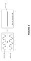
- FIG. 3 shows the destructive effect (e.g., destructive effect 308 ) of combining two waves of different (e.g., equal amplitude but opposite phase) intensities, according to one or more embodiments.
- wave X 302 and wave Y 304 (having equal amplitudes but opposite phases) combine destructively to cancel each other.
- the destructive effect 308 produces wave Z 306 of zero amplitude.
- FIG. 4 shows photo detection at multiple locations, according to one or more embodiments.
- photodetection data originating from source 400 and ranging across a set of frequency channels, may be collected.
- source 400 include but are not limited to a planet, a star, and any other extraterrestrial body.
- the extraterrestrial body may be a natural object existing outside the earth and outside the earth's atmosphere.
- the photodetection data collected may be communicated to a computational station 404 and collected thereat.
- computational station 404 may be configured to calculate the correlation between photodetection data in each of the frequency channels/bands. In one or more embodiments, computational station 404 may also be configured to calculate a time average of the correlation between the photodetection data in each frequency band. In one or more embodiments, computational station 404 may further be configured to determine the average over frequency channels to arrive at measurements of mutual coherence magnitude for each pair of telescopes (e.g., light gathering telescopes 402 1-N ). Further, in one or more embodiments, computational station 404 may be configured to compute imaging data through phase retrieval techniques.
- entry pupil processing may be used to obtain ultra-fine resolution imaging.
- computational station 404 may be configured to compute mutual coherence information between pairs of light gathering telescopes 402 1-N . Further, the computational station 404 may be configured to compute the desired image of the source 400 .
- the system described in FIG. 4 may eliminate the need for extreme-precision relative positioning control for the path length control of the light gathering telescopes 402 1-N and the need for transporting collected beams at the light gathering telescopes 402 1-N to a central combiner. Light collecting telescopes 402 1-N may be independent and even the propagation of light to the central combiner may not be required.
- signal-to-noise characteristics of the coherence may be obtained through a system similar to the one shown in FIG. 4 .
- partial coherence may be used to attenuate a parent star of an extrasolar planet (exoplanet).
- exoplanet extrasolar planet
- a multi-spacecraft distributed formation may consist of several free-flying spacecraft, with each spacecraft carrying a light gathering telescope (e.g., light gathering telescope 402 1-N ).
- the light gathering telescope being carried by the spacecraft may be smaller in comparison to a telescope that is based on the ground and a baseline associated therewith.
- the spacecraft may execute maneuvers.
- the light gathering telescopes on the spacecraft may collect beams from a light source.
- the beams collected from selected pairs of telescopes may interfere to produce a continuous sequence of measurements to form interferometric images.
- the aforementioned may enable design of a free flying space-borne interferometer that is used to obtain improved image quality for de-convolved images produced by interferometry.
- formulation of the image acquisition process relevant to the multi-spacecraft formation may lead to the development of an image quality metric based on evolving modulation transfer function (MTF) of the system and a signal-to-noise ratio.
- MTF modulation transfer function
- the MTF function may be a transfer of modulation from the source 400 to the image that is computed at the computational station 400 .
- the signal-to-noise ratio may be a ratio of the power of a signal from the source 400 to the noise associated therewith.
- an optimal imaging problem may be based on analysis of the system's resolution in the spatial frequency domain.
- quantum superposition may be an event that can be realized in two or more indistinguishable ways, with the system state of the system being a superposition of each way simultaneously.
- the photodetection data from the light gathering telescopes 402 1-N may be subject to quantum superposition when considered in pairs and other combinations.
- FIG. 5 illustrates a telescope composition 500 .
- each of the light gathering telescopes 402 1-N may include a photo detection unit 502 and a time history recording apparatus 504 .
- photo detection unit 502 may detect photons from the source 400 .
- the time history recording apparatus 504 may record time of receiving the photons from the source 400 .
- recording of the time of receiving the photons from the source 400 may be relevant to the computation that needs to be made at the computational station 404 .
- the light collected by the light gathering telescopes 402 1-N may be transferred to photodetection apparatus (not shown) and further transferred to associated electronics to aid in the computation made at the computational station 404 .
- FIG. 6 shows a process flow diagram detailing the operations involved in computing imaging data at the computational station 404 of FIG. 4 , according to one or more embodiments.
- operation 602 may involve receiving photodetection data encompassing a set of frequency channels at computational station 404 .
- operation 604 may involve determining correlation between the photodetection data in each of the frequency channels/bands.
- operation 606 may involve determining a time average of the correlation between the photodetection data in each frequency band.
- operation 608 may involve determining an average over the frequency channels to arrive at measurements of mutual coherence magnitude for each pair of telescopes (e.g., light gathering telescopes 402 1-N ).
- operation 610 may then involve computing an imaging data through phase retrieval techniques.
- the image thus obtained may be better than the results obtained using amplitude interferometry.
- utilization of the system disclosed in FIGS. 4-6 may not require precision (e.g., nanometer level) control of the relative positions of devices in the system and may be less expensive in comparison to a system that uses amplitude interferometry.
- the system of FIG. 4 may be superior to a system utilizing amplitude interferometry when the number of apertures may increase to, for example, 10 apertures.
- the superiority may be due to the absence of beam splitting and throughput losses that may be present in a system utilizing amplitude interferometry.
- FIG. 7 shows an interferometer 700 , according to one or more embodiments.
- the interferometer 700 may be used to measure the angular diameter of extraterrestrial bodies.
- interferometer 700 may include two aerials (or, antennas) A 1 702 and A 2 704 associated with detector 706 and detector 708 respectively.
- signals from the two aerials A 1 702 and A 2 704 may be detected (e.g., through detector 706 and detector 708 ) independently and the correlation between low frequency outputs of the detector(s) recorded.
- correlation between the intensity fluctuations of the two signals may be measured.
- the two signals from the aerials may not be required to be combined before detection.
- relative phase between the two signals may not be required to be preserved.
- baseline may be a projected separation between any two light gathering telescopes (e.g., any two of light gathering telescopes 402 1-N ) as seen from the source 400 .
- the system of FIGS. 4 , 5 and/or 7 may be designed to work with large baselines.
- the signals detected by the detectors 706 and 708 may be passed through low pass filters (e.g., low-pass filter 710 and low-pass filter 712 respectively).
- low frequency signals from the low pass filters may be transferred to a correlator 714 to determine the correlation. Further, the correlation determined between the two signals may be recorded in a recorder 716 .
- FIG. 8 shows an interferometer with mirrors 800 , according to one or more embodiments.
- light beams may be incident on mirrors M 1 806 and M 2 808 (instead on the aerials as seen in interferometer 700 of FIG. 7 ).
- detectors e.g., 706 and 708
- cells C 1 802 and C 2 804 may be photoelectric cells, light detectors and/or phototubes whose electrical output varies with a variation in the incident light beams.
- the light beams incident on the mirrors M 1 806 and M 2 808 may be reflected onto cells C 1 802 and C 2 804 to measure the correlation between the fluctuations in the current as a function of a distance between the two mirrors M 1 806 and M 2 808 .
- the correlation may be computed in a correlator 810 .
- the correlation calculated by the correlator 810 may be recorded in a recorder 812 .
- FIG. 9 shows a simplified architecture of an interferometer 900 , according to one or more embodiments.
- a light source 902 may be formed by a mercury arc.
- beams from the light source 902 may be passed through the lens 904 .
- a low frequency beam may be isolated through a system of filters that include, for example, a combination of filter 908 , aperture 906 and filter 910 .
- the low frequency beam may be divided into two parts by a half silvered mirror 912 to illuminate cathodes of photomultiplier tubes 914 and 916 .
- apertures of the photomultiplier tubes ( 914 , 916 ) may be identical.
- the cathodes of the photomultiplier tubes 914 and 916 may not be located at equal distances from the light source 902 .
- fluctuations of output currents from the photomultiplier tubes 914 and 916 may be amplified through amplifiers 918 and 920 and multiplied together in a correlator 922 .
- average value of the product may be recorded in an integrator 924 .
- the average value that is recorded by the integrator 924 may be a measure of the correlation in the fluctuations.
- FIG. 10 shows schematic view of a general planet imaging architecture 1000 , according to one embodiment.
- individual spacecrafts 1002 1-4 may be light collectors and/or beam collectors.
- the individual spacecraft 1002 1-4 may carry light gathering telescopes to collect light and/or beams from an extraterrestrial body 1014 .
- the individual spacecrafts 1002 1-4 may not move in a single plane.
- the individual spacecrafts 1002 1-4 may be independent of each other.
- cancelling collectors 1006 1-4 may be placed appropriately to negate the effect of any light emitting bodies that may be closer to the extraterrestrial body 1014 in comparison to the individual spacecraft 1002 1-4 .
- the individual spacecraft 1002 1-4 and the cancelling collectors 1006 1-4 may not be in any alignment and/or formation.
- photodetection data from the individual spacecraft 1002 1-4 and cancelling collectors 1006 1-4 may be collected at a pod combiner 1004 and pod combiner 1008 .
- an imaging combiner 1010 may collect data from the pod combiners 1004 and 1008 . In one or more embodiments, the imaging combiner 1010 may determine pairs of telescopes on individual spacecrafts 1002 1-4 and the imaging data that is collected at the imaging combiner 1010 is transferred to a central processing station 1012 .
- the system disclosed in FIG. 10 may include a phasing beacon (not shown). In one or more embodiments, use of devices such as a phasing beacon may negate the need to propagate beams collected at individual spacecrafts 1002 1-4 and cancelling collectors 1006 1-4 to combining stations that need to move at a specified distance and alignment from the individual spacecrafts 1002 1-4 that carry the telescopes.
- the system of FIG. 4 may be used for extrasolar planet detection, particularly terrestrial planets at a range of 15 parsec or less. 1 parsec may be derived from the smallest angle measurement of 1/3,600th of a degree.
- system considered may include several modest-sized telescopes (light collectors), each equipped with photodetection apparatus and the means to record the photodetector signal time-history.
- the cross-correlations of the individual light collector photodetection histories may be computed to yield, in turn, a collection of values for the magnitudes of the mutual coherence of the target scene at various measurement baselines. Further, computed coherence magnitudes may be used to infer the apparent motion of the target star.
- the resolution of the target star motion may be very fine.
- Signal-to-noise ratio (SNR) of a single coherence magnitude measurement may be computed.
- SNR Signal-to-noise ratio
- the SNR may be computed to determine the planet orbit parameters.
- quantum photon entanglement may be used to increase the sensitivity of the interferometer measurement.
- the quantum entangled photon interferometer approach may apply to many types of interferometers.
- a generic classical interferometer may have a statistical-sampling shot-noise limited sensitivity that scales like 1N, where N is the number of particles (e.g., photons, electrons, atoms, neutrons) passing through the interferometer per unit time.
- quantum correlations may improve the interferometer sensitivity between the particles by a factor of a square-root-of-N, to scale like 1/N. 1/N may be the limit imposed by the Heisenberg Uncertainty Principle.
- optical interferometers may operate at a specified optical power, and the quantum sensitivity boost corresponds to an order-of-magnitude improvement of SNR.
- beams collected at an aperture of a telescope may be converted to data. Further, the data may be transferred to a suitable location to calculate the mutual coherence.
- the mutual coherence may be the phase relationship between photons collected at a pair of telescopes.
- the desired image of the extraterrestrial body (e.g., 1014 ) and/or other image may be computed and used as a means for entry pupil processing.
- entry pupil may represent the entry nodal point of a lens.
- computing station 404 may be a computing system including a memory and a processor communicatively coupled to the memory (processor and memory not shown because of obviousness reasons).
- the processor may be configured to execute all instructions associated with the computation described with reference to FIG. 6 .
Landscapes
- Physics & Mathematics (AREA)
- Astronomy & Astrophysics (AREA)
- General Physics & Mathematics (AREA)
- Optics & Photonics (AREA)
- Instruments For Measurement Of Length By Optical Means (AREA)
Abstract
Description
<detector C/point A><detector D/point B>
and <detector D/point A><detector C/point B>respectively.
Claims (20)
Priority Applications (1)
| Application Number | Priority Date | Filing Date | Title |
|---|---|---|---|
| US13/418,333 US9052497B2 (en) | 2011-03-10 | 2012-03-12 | Computing imaging data using intensity correlation interferometry |
Applications Claiming Priority (2)
| Application Number | Priority Date | Filing Date | Title |
|---|---|---|---|
| US201161451145P | 2011-03-10 | 2011-03-10 | |
| US13/418,333 US9052497B2 (en) | 2011-03-10 | 2012-03-12 | Computing imaging data using intensity correlation interferometry |
Publications (2)
| Publication Number | Publication Date |
|---|---|
| US20120232842A1 US20120232842A1 (en) | 2012-09-13 |
| US9052497B2 true US9052497B2 (en) | 2015-06-09 |
Family
ID=46796852
Family Applications (1)
| Application Number | Title | Priority Date | Filing Date |
|---|---|---|---|
| US13/418,333 Expired - Fee Related US9052497B2 (en) | 2011-03-10 | 2012-03-12 | Computing imaging data using intensity correlation interferometry |
Country Status (1)
| Country | Link |
|---|---|
| US (1) | US9052497B2 (en) |
Cited By (1)
| Publication number | Priority date | Publication date | Assignee | Title |
|---|---|---|---|---|
| US9769411B2 (en) * | 2004-02-23 | 2017-09-19 | Sony Corporation | Solid-state image pickup device and method for driving the same in solid-state imaging pickup device and method for driving the same in a number of modes |
Families Citing this family (2)
| Publication number | Priority date | Publication date | Assignee | Title |
|---|---|---|---|---|
| US9407467B2 (en) * | 2013-10-23 | 2016-08-02 | The United States Of America, As Represented By The Secretary Of The Navy | Method and apparatus for transmitting and receiving information wirelessly using intensity interferometry |
| US11523097B2 (en) * | 2019-03-22 | 2022-12-06 | Universita' Degli Studi Di Bari Aldo Moro | Process and apparatus for the capture of plenoptic images between arbitrary planes |
Citations (186)
| Publication number | Priority date | Publication date | Assignee | Title |
|---|---|---|---|---|
| US3160696A (en) * | 1960-12-30 | 1964-12-08 | Ibm | Optical phase angle measuring apparatus |
| US3808550A (en) | 1969-12-15 | 1974-04-30 | Bell Telephone Labor Inc | Apparatuses for trapping and accelerating neutral particles |
| US4623930A (en) | 1983-12-29 | 1986-11-18 | Matsushita Electric Industrial Co., Ltd. | Camera apparatus |
| US4630184A (en) | 1984-04-16 | 1986-12-16 | Fiat Auto S.P.A. | Motor vehicle lamp, and a light unit for motor vehicles incorporating such lamps |
| US4710817A (en) | 1984-12-26 | 1987-12-01 | Nippon Hoso Kyokai | Solid state image sensor |
| US4759628A (en) | 1985-03-06 | 1988-07-26 | Hitachi, Ltd. | Wavelength scanning interferometry and interferometer employing laser diode |
| US4979221A (en) | 1987-12-23 | 1990-12-18 | Agence Spatiale Europeene | Method and apparatus for sub-pixel centroiding of a photon event |
| US5021854A (en) | 1987-12-03 | 1991-06-04 | Xsirius Photonics, Inc. | Silicon avalanche photodiode array |
| EP0451852A1 (en) | 1990-04-11 | 1991-10-16 | Kabushiki Kaisha Toshiba | Avalanche photodiode having guard ring and method of manufacturing the same |
| US5198660A (en) | 1990-08-30 | 1993-03-30 | Fuji Electric Co., Ltd. | Optical sensing circuit including an integral capacity |
| US5212382A (en) | 1990-12-13 | 1993-05-18 | Keiji Sasaki | Laser trapping and method for applications thereof |
| US5262871A (en) | 1989-11-13 | 1993-11-16 | Rutgers, The State University | Multiple resolution image sensor |
| US5301240A (en) | 1990-12-14 | 1994-04-05 | Battelle Memorial Institute | High-speed video instrumentation system |
| US5308976A (en) | 1991-06-01 | 1994-05-03 | Research Development Corp. Of Japan | Method for multi-beam manipulation of microparticles |
| US5363190A (en) | 1992-09-07 | 1994-11-08 | Olympus Optical Co., Ltd. | Method and apparatus for optical micro manipulation |
| US5412422A (en) | 1991-12-12 | 1995-05-02 | Kabushiki Kaisha Photron | High speed imaging apparatus |
| US5448056A (en) | 1993-02-10 | 1995-09-05 | Fuji Electric Co., Ltd. | Photoelectric converting circuit having an amplification factor |
| US5467128A (en) | 1994-01-19 | 1995-11-14 | The Regents Of The University Of California, Office Of Technology Transfer | High speed imager test station |
| US5468954A (en) | 1991-06-21 | 1995-11-21 | Canon Kabushiki Kaisha | Photo-electric converter having variable accumulation time |
| US5557542A (en) | 1993-08-13 | 1996-09-17 | Kabushiki Kaisha Toshiba | Image storage apparatus |
| US5565915A (en) | 1993-06-15 | 1996-10-15 | Matsushita Electric Industrial Co., Ltd. | Solid-state image taking apparatus including photodiode and circuit for converting output signal of the photodiode into signal which varies with time at variation rate depending on intensity of light applied to the photodiode |
| US5631704A (en) | 1994-10-14 | 1997-05-20 | Lucent Technologies, Inc. | Active pixel sensor and imaging system having differential mode |
| US5650643A (en) | 1994-03-30 | 1997-07-22 | Nec Corporation | Device for receiving light used in CCD image sensor or the like |
| US5665959A (en) | 1995-01-13 | 1997-09-09 | The United States Of America As Represented By The Administrator Of The National Aeronautics And Space Adminstration | Solid-state image sensor with focal-plane digital photon-counting pixel array |
| US5705807A (en) | 1994-10-24 | 1998-01-06 | Nissan Motor Co., Ltd. | Photo detecting apparatus for detecting reflected light from an object and excluding an external light componet from the reflected light |
| US5708471A (en) | 1993-03-25 | 1998-01-13 | Nec Corporation | Image sensors and driving method thereof |
| US5754690A (en) | 1995-10-27 | 1998-05-19 | Xerox Corporation | Position sensitive detector based image conversion system capable of preserving subpixel information |
| US5777669A (en) | 1993-02-19 | 1998-07-07 | Fuji Xerox Co., Ltd. | Image reading device |
| US5841126A (en) | 1994-01-28 | 1998-11-24 | California Institute Of Technology | CMOS active pixel sensor type imaging system on a chip |
| US5892541A (en) | 1996-09-10 | 1999-04-06 | Foveonics, Inc. | Imaging system and method for increasing the dynamic range of an array of active pixel sensor cells |
| WO1999018717A1 (en) | 1997-10-06 | 1999-04-15 | Photobit, Inc. | Quantum efficiency improvements in active pixel sensors |
| US5923369A (en) | 1997-07-23 | 1999-07-13 | Foveonics, Inc. | Active pixel sensor cell with differential amplifier and array including same |
| US5978025A (en) | 1995-11-21 | 1999-11-02 | Stmicroelectronics S.R.L. | Adaptive optical sensor |
| US5994690A (en) * | 1997-03-17 | 1999-11-30 | Kulkarni; Manish D. | Image enhancement in optical coherence tomography using deconvolution |
| US6028300A (en) | 1998-02-11 | 2000-02-22 | Rhoads; Geoffrey B. | Methods and apparatus for multi-sensor astronomical imaging |
| US6078037A (en) | 1998-04-16 | 2000-06-20 | Intel Corporation | Active pixel CMOS sensor with multiple storage capacitors |
| US6115065A (en) | 1995-11-07 | 2000-09-05 | California Institute Of Technology | Image sensor producing at least two integration times from each sensing pixel |
| US6118482A (en) | 1997-12-08 | 2000-09-12 | Intel Corporation | Method and apparatus for electrical test of CMOS pixel sensor arrays |
| EP1041637A1 (en) | 1998-09-22 | 2000-10-04 | Shimadzu Corporation | High-speed imaging device |
| US6130423A (en) | 1998-07-10 | 2000-10-10 | Pixel Cam, Inc. | Method and apparatus for a CMOS image sensor with a distributed amplifier |
| US6130713A (en) | 1997-06-27 | 2000-10-10 | Foveonics, Inc. | CMOS active pixel cell with self reset for improved dynamic range |
| US6157016A (en) | 1997-09-30 | 2000-12-05 | Intel Corporation | Fast CMOS active-pixel sensor array readout circuit with predischarge circuit |
| US6181375B1 (en) | 1991-07-22 | 2001-01-30 | Kabushiki Kaisha Photron | Image recording apparatus capable of selecting partial image areas for video readout |
| US6236449B1 (en) | 1998-03-19 | 2001-05-22 | Nikon Corporation | Illumination optical apparatus and exposure apparatus |
| EP1104178A1 (en) | 1999-11-29 | 2001-05-30 | Agilent Technologies Inc. (a Delaware Corporation) | Active pixel sensor with enhanced reset |
| US6248990B1 (en) | 1996-10-15 | 2001-06-19 | Simage Oy | Radiation imaging device with an array of image cells |
| US6282028B1 (en) | 1999-06-26 | 2001-08-28 | Hilti Aktiengesellschaft | Beamsplitter |
| US6297488B1 (en) | 1999-04-29 | 2001-10-02 | National Research Council Of Canada | Position sensitive light spot detector |
| US20010030277A1 (en) | 1993-03-01 | 2001-10-18 | Pinecone Imaging Corporation | High resolution imaging instrument |
| EP1148348A2 (en) | 2000-04-18 | 2001-10-24 | Marconi Medical Systems, Inc. | Nuclear camera |
| US6330030B1 (en) | 1998-01-05 | 2001-12-11 | Intel Corporation | Digital image sensor with low device count per pixel analog-to-digital conversion |
| US20010052941A1 (en) | 1995-08-11 | 2001-12-20 | Yoshiyuki Matsunaga | Image system, solid-state imaging semiconductor integrated circuit device used in the image system, and difference output method used for the image system |
| US20020024058A1 (en) | 2000-08-16 | 2002-02-28 | Marshall Gillian F. | Photodetector circuit |
| US6359274B1 (en) | 1999-01-25 | 2002-03-19 | Gentex Corporation | Photodiode light sensor |
| US6366312B1 (en) | 1998-06-09 | 2002-04-02 | Intel Corporation | Testing components in digital imaging devices |
| US6476864B1 (en) | 1998-05-11 | 2002-11-05 | Agilent Technologies, Inc. | Pixel sensor column amplifier architecture |
| US20030010896A1 (en) | 2001-06-25 | 2003-01-16 | Noriyuki Kaifu | Image sensing apparatus capable of outputting image by converting resolution by adding and reading out a plurality of pixels, its control method, and image sensing system |
| US20030103212A1 (en) | 2001-08-03 | 2003-06-05 | Volker Westphal | Real-time imaging system and method |
| US6580454B1 (en) | 1998-11-18 | 2003-06-17 | Agilent Technologies, Inc. | CMOS active pixel sensor having in-pixel local exposure control |
| US6587145B1 (en) | 1998-08-20 | 2003-07-01 | Syscan Technology (Shenzhen) Co., Ltd. | Image sensors generating digital signals from light integration processes |
| US6603607B2 (en) | 2000-04-07 | 2003-08-05 | Nikon Corporation | Minute particle optical manipulation method and apparatus |
| US6631022B1 (en) | 1999-05-28 | 2003-10-07 | Sony Corporation | Optical device, a fabrication method thereof, a driving method thereof and a camera system |
| US6633028B2 (en) | 2001-08-17 | 2003-10-14 | Agilent Technologies, Inc. | Anti-blooming circuit for CMOS image sensors |
| US6633335B1 (en) | 1998-02-28 | 2003-10-14 | Hyundai Electronics Industries Co., Ltd. | CMOS image sensor with testing circuit for verifying operation thereof |
| US20030193771A1 (en) | 2002-04-12 | 2003-10-16 | Sun Microsystems, Inc. | On-chip decoupling capacitors designed for a 0.11 micron and beyond dual gate oxide CMOS technology |
| US6677996B1 (en) | 1999-04-21 | 2004-01-13 | Pictos Technologies, Inc. | Real time camera exposure control |
| US20040058553A1 (en) | 2002-09-19 | 2004-03-25 | Semiconductor Energy Laboratory Co., Ltd | Beam homogenizer and laser irradiation apparatus and method of manufacturing semiconductor device |
| US20040189999A1 (en) | 2003-03-06 | 2004-09-30 | De Groot Peter J. | Profiling complex surface structures using scanning interferometry |
| US6825936B2 (en) | 2000-08-23 | 2004-11-30 | Lmi Technologies, Inc. | High speed camera based sensors |
| US20040243656A1 (en) | 2003-01-30 | 2004-12-02 | Industrial Technology Research Institute | Digital signal processor structure for performing length-scalable fast fourier transformation |
| US6831263B2 (en) | 2002-06-04 | 2004-12-14 | Intel Corporation | Very high speed photodetector system using a PIN photodiode array for position sensing |
| US20050012033A1 (en) | 2003-05-02 | 2005-01-20 | Alvin Stern | Digital photon-counting geiger-mode avalanche photodiode solid-state monolithic intensity imaging focal-plane with scalable readout circuitry |
| US6873282B1 (en) | 2004-03-04 | 2005-03-29 | Charles Douglas Murphy | Differential time-to-threshold A/D conversion in digital imaging arrays |
| US6884982B2 (en) | 2002-02-19 | 2005-04-26 | Massachusetts Institute Of Technology | Methods and apparatus for improving resolution and reducing the effects of signal coupling in an electronic imager |
| US6909462B1 (en) | 1998-03-18 | 2005-06-21 | Honda Giken Kogko Kabushiki Kaisha | Photosensor circuit capable of detecting minute light signal in high precision and image sensor utilizing photosensor circuit |
| WO2005069040A1 (en) | 2004-01-13 | 2005-07-28 | Koninklijke Philips Electronics, N.V. | Analog to digital conversion shift error correction |
| US6927433B2 (en) | 2001-06-28 | 2005-08-09 | Isetec, Inc | Active pixel image sensor with two transistor pixel, in-pixel non-uniformity correction, and bootstrapped reset lines |
| US6927796B2 (en) | 2001-09-24 | 2005-08-09 | The Board Of Trustees Of The Leland Stanford Junior University | CMOS image sensor system with self-reset digital pixel architecture for improving SNR and dynamic range |
| US20050248675A1 (en) | 1998-04-30 | 2005-11-10 | Canon Kabushiki Kaisha | Arrangement of circuits in pixels, each circuit shared by a plurality of pixels, in image sensing apparatus |
| US6977685B1 (en) | 1999-02-26 | 2005-12-20 | Massachusetts Institute Of Technology | Single-chip imager system with programmable dynamic range |
| US6982403B2 (en) | 2002-03-27 | 2006-01-03 | Omnivision Technologies, Inc. | Method and apparatus kTC noise cancelling in a linear CMOS image sensor |
| US20060044451A1 (en) | 2004-08-30 | 2006-03-02 | Eastman Kodak Company | Wide angle lenslet camera |
| US7053947B2 (en) | 1998-06-02 | 2006-05-30 | Samsung Electronics Co., Ltd. | Methods for improving sensitivity of CMOS active pixel sensors |
| US20060131484A1 (en) | 2004-12-17 | 2006-06-22 | Mark Peting | High-dynamic range image sensors |
| US20060131480A1 (en) | 2004-01-12 | 2006-06-22 | Edoardo Charbon | Method for controlling the spectral response of light sensitive elements, and image sensor with a controllable spectral response |
| US20060175529A1 (en) | 2003-11-06 | 2006-08-10 | Harmon Eric S | Large-area detector |
| US7115963B2 (en) | 2002-12-09 | 2006-10-03 | Quantum Semiconductor Llc | Circuitry for image sensors with avalanche photodiodes |
| US20060231742A1 (en) | 2005-04-14 | 2006-10-19 | Forsyth Keith W | Method and apparatus for providing non-linear, passive quenching of avalanche currents in Geiger-mode avalanche photodiodes |
| US7126838B2 (en) | 2003-09-04 | 2006-10-24 | Canon Kabushiki Kaisha | Readout circuit, solid state image pickup device using the same circuit, and camera system using the same |
| US20060245071A1 (en) | 2005-04-29 | 2006-11-02 | Agilent Technologies | Lens correction element, system and method |
| US20070022110A1 (en) | 2003-05-19 | 2007-01-25 | Saora Kabushiki Kaisha | Method for processing information, apparatus therefor and program therefor |
| US7205522B2 (en) | 2005-05-18 | 2007-04-17 | Alexander Krymski D. B. A Alexima | Pixel circuit for image sensor |
| US20070084986A1 (en) | 2005-10-18 | 2007-04-19 | Dialog Semiconductor Manufacturing Ltd | Multiple photosensor pixel |
| WO2007043036A1 (en) | 2005-10-11 | 2007-04-19 | Prime Sense Ltd. | Method and system for object reconstruction |
| US7233350B2 (en) | 2002-01-05 | 2007-06-19 | Candela Microsystems, Inc. | Image sensor with interleaved image output |
| US7245250B1 (en) | 2005-08-16 | 2007-07-17 | Itt Manufacturing Enterprises, Inc. | Synthetic aperture radar image compression |
| US7262402B2 (en) | 2005-02-14 | 2007-08-28 | Ecole Polytechnique Federal De Lausanne | Integrated imager circuit comprising a monolithic array of single photon avalanche diodes |
| US7277129B1 (en) | 2002-10-31 | 2007-10-02 | Sensata Technologies, Inc. | Pixel design including in-pixel correlated double sampling circuit |
| US7280221B2 (en) | 2004-02-10 | 2007-10-09 | Optovue, Inc. | High efficiency low coherence interferometry |
| US7286174B1 (en) | 2001-06-05 | 2007-10-23 | Dalsa, Inc. | Dual storage node pixel for CMOS sensor |
| US7319486B2 (en) | 2001-09-13 | 2008-01-15 | Honda Giken Kogyo K.K. | High-speed event imaging device |
| US7319423B2 (en) | 2002-07-31 | 2008-01-15 | Quantum Semiconductor Llc | Multi-mode ADC and its application to CMOS image sensors |
| US7324146B2 (en) | 2003-01-22 | 2008-01-29 | Seiko Epson Corporation | Image processing device, image processing method and solid-state image-pickup device |
| US20080106603A1 (en) | 2006-10-18 | 2008-05-08 | Southern Vision Systems, Inc. | System and method for high-speed image-cued triggering |
| US7391004B2 (en) | 2006-03-31 | 2008-06-24 | Sanyo Electric Co., Ltd. | Photo detecting apparatus |
| US7426036B2 (en) | 2005-07-08 | 2008-09-16 | Imalux Corporation | Common path frequency domain optical coherence reflectometer and common path frequency domain optical coherence tomography device |
| US20080231339A1 (en) | 2007-03-23 | 2008-09-25 | Deschamps Pierre D | Double quench circuit for an avalanche current device |
| US20080230723A1 (en) | 2003-04-24 | 2008-09-25 | Semiconductor Energy Laboratory Co., Ltd. | Beam homogenizer, laser irradiation apparatus, and method for manufacturing semiconductor device |
| US20080252762A1 (en) | 2007-04-13 | 2008-10-16 | Konica Minolta Holdings, Inc. | Solid-state image sensing device, method for driving solid-state image sensing device, and image sensing system incorporated with solid-state image sensing device |
| US20080279441A1 (en) | 2005-03-29 | 2008-11-13 | Yuichiro Matsuo | Cell-Image Analysis Method, Cell-Image Analysis Program, Cell-Image Analysis Apparatus, Screening Method, and Screening Apparatus |
| WO2008151155A2 (en) | 2007-05-31 | 2008-12-11 | Board Of Regents, The University Of Texas System | Polarization-sensitive spectral interferometry |
| US7466429B2 (en) | 2003-03-06 | 2008-12-16 | Zygo Corporation | Profiling complex surface structures using scanning interferometry |
| US7483058B1 (en) | 2003-08-04 | 2009-01-27 | Pixim, Inc. | Video imaging system including a digital image sensor and a digital signal processor |
| US7502107B2 (en) | 2003-08-22 | 2009-03-10 | Secretary, Department Of Atomic Energy, Government Of India | Apparatus and method for transport of microscopic object(s) |
| US7504616B2 (en) | 2006-04-10 | 2009-03-17 | Panasonic Corporation | Exposure device and image forming apparatus using the same |
| WO2009042901A1 (en) | 2007-09-28 | 2009-04-02 | Regents Of The University Of Minnesota | Image sensor with high dynamic range imaging and integrated motion detection |
| US7522288B2 (en) | 2006-07-21 | 2009-04-21 | Zygo Corporation | Compensation of systematic effects in low coherence interferometry |
| US7547872B2 (en) | 2005-02-14 | 2009-06-16 | Ecole Polytechnique Federale De Lausanne | Integrated circuit comprising an array of single photon avalanche diodes |
| US20090182528A1 (en) | 2007-12-14 | 2009-07-16 | De Groot Peter | Analyzing surface structure using scanning interferometry |
| US7593651B2 (en) | 2002-03-14 | 2009-09-22 | Ericsson Ab | Control of avalanche photodiodes bias voltage |
| WO2009115956A2 (en) | 2008-03-19 | 2009-09-24 | Koninklijke Philips Electronics N.V. | Single photon radiation detector |
| US20090244971A1 (en) | 2008-04-01 | 2009-10-01 | University Of Michigan | Memory cell structure, a memory device employing such a memory cell structure, and an integrated circuit having such a memory device |
| US7598998B2 (en) | 2005-09-30 | 2009-10-06 | Honeywell International Inc. | Method and system for increasing the effective dynamic range of a random-access pixel sensor array |
| US20090256735A1 (en) | 2008-04-09 | 2009-10-15 | Jan Bogaerts | Analog-to-digital conversion in pixel arrays |
| US7619674B2 (en) | 2005-01-24 | 2009-11-17 | Korea Advanced Institute Of Science And Technology | CMOS image sensor with wide dynamic range |
| US7623173B2 (en) | 2004-02-23 | 2009-11-24 | Sony Corporation | Solid-state image pickup device having analog-digital converters configured to sum values of multiple pixels in the array and method for driving the same |
| US7626624B2 (en) | 2001-05-29 | 2009-12-01 | Samsung Electronics Co., Ltd. | Serial output from a CMOS imager |
| US20100026838A1 (en) | 2006-11-20 | 2010-02-04 | Ben Gurion University Of The Negev Research And Development Authority | Optical pixel and image sensor |
| US7697051B2 (en) | 2001-10-24 | 2010-04-13 | Aptina Imaging Corporation | Image sensor with pixels having multiple capacitive storage elements |
| US7696463B2 (en) | 2005-12-01 | 2010-04-13 | Honda Motor Co., Ltd. | Photosensor circuit presenting linear and logarithimic output characteristics and image sensor using the same |
| US7701499B2 (en) | 2004-12-07 | 2010-04-20 | Bright Imaging Ltd. | Method and apparatus for imaging of scenes having large intensity variance |
| US7718953B2 (en) | 2006-04-12 | 2010-05-18 | University Of Delaware | Electromagnetic/optical tweezers using a full 3D negative-refraction flat lens |
| US7728893B2 (en) | 2004-11-02 | 2010-06-01 | Japan Science And Technology Agency | Imaging device and method for reading signals from such device |
| US20100181491A1 (en) | 2009-01-16 | 2010-07-22 | Karim Karim S | Digitizer for a digital imaging system |
| US20100182011A1 (en) | 2007-06-25 | 2010-07-22 | Koninklijke Philips Electronics N.V. | Photodiode self-test |
| US20100204459A1 (en) | 2007-08-27 | 2010-08-12 | The Regents Of The University Of California | Systems and methods for producing multi-component colloidal structures |
| US20100213353A1 (en) | 2009-02-25 | 2010-08-26 | Bart Dierickx | Analog photon counting |
| US7795650B2 (en) | 2008-12-09 | 2010-09-14 | Teledyne Scientific & Imaging Llc | Method and apparatus for backside illuminated image sensors using capacitively coupled readout integrated circuits |
| US20100245809A1 (en) | 2007-03-15 | 2010-09-30 | Johns Hopkins University | Deep submicron and nano cmos single photon photodetector pixel with event based circuits for readout data-rate reduction communication system |
| US20100271517A1 (en) | 2009-04-24 | 2010-10-28 | Yannick De Wit | In-pixel correlated double sampling pixel |
| US20100270462A1 (en) | 2008-04-08 | 2010-10-28 | Robert Sigurd Nelson | Slit and slot scan, SAR, and compton devices and systems for radiation imaging |
| US7847846B1 (en) | 2006-05-16 | 2010-12-07 | University Of Rochester | CMOS image sensor readout employing in-pixel transistor current sensing |
| US20100315709A1 (en) | 2007-02-07 | 2010-12-16 | Baer Stephen C | Forming light beams and patterns with zero intensity central points |
| US7868665B2 (en) | 2002-03-05 | 2011-01-11 | Nova R&D, Inc. | Integrated circuit and sensor for imaging |
| US7889355B2 (en) | 2007-01-31 | 2011-02-15 | Zygo Corporation | Interferometry for lateral metrology |
| US7911520B2 (en) | 2001-01-30 | 2011-03-22 | Nippon Telegraph And Telephone Corporation | Data conversion/output apparatus for digitalizing sensor data and outputting through a sensor array |
| US20110090385A1 (en) | 2008-06-04 | 2011-04-21 | Honda Motor Co., Ltd. | Imaging device |
| US7940317B2 (en) | 2004-11-12 | 2011-05-10 | Stmicroelectronics Ltd. | Image sensor having a pixel array with serial readout |
| US7956912B2 (en) | 1998-10-29 | 2011-06-07 | Micron Technology, Inc. | Active pixel sensor with mixed analog and digital signal integration |
| US20110188120A1 (en) | 2010-01-29 | 2011-08-04 | Beam Engineering For Advanced Measurement Co. | Broadband optics for manipulating light beams and images |
| US7999945B2 (en) | 2007-07-18 | 2011-08-16 | The George Washington University | Optical coherence tomography / acoustic radiation force imaging probe |
| US8026471B2 (en) | 2008-07-23 | 2011-09-27 | Princeton Lightwave, Inc. | Single-photon avalanche detector-based focal plane array |
| US20110249148A1 (en) | 2008-12-22 | 2011-10-13 | Koninklijke Philips Electronics N.V. | Cmos imager with single photon counting capability |
| US20110260039A1 (en) | 2008-10-20 | 2011-10-27 | Boyd Fowler | Imaging Array with Modulated Pixels |
| CN202048982U (en) | 2011-02-19 | 2011-11-23 | 欧阳国平 | A laser beam parameter measuring device |
| US8077328B2 (en) | 2009-07-06 | 2011-12-13 | Gammex, Inc. | Variable color incoherent alignment line and cross-hair generator |
| US8089036B2 (en) | 2009-04-30 | 2012-01-03 | Omnivision Technologies, Inc. | Image sensor with global shutter and in pixel storage transistor |
| US8089522B2 (en) | 2007-09-07 | 2012-01-03 | Regents Of The University Of Minnesota | Spatial-temporal multi-resolution image sensor with adaptive frame rates for tracking movement in a region of interest |
| US8093624B1 (en) | 2006-02-15 | 2012-01-10 | Massachusetts Institute Of Technology | High fill-factor avalanche photodiode |
| US8120687B2 (en) | 2007-02-08 | 2012-02-21 | Fujitsu Limited | Signal reading method, signal reading circuit, and image sensor |
| US20120056078A1 (en) | 2010-09-07 | 2012-03-08 | King Abdulaziz City Science And Technology | Coordinated in-pixel light detection method and apparatus |
| US20120057059A1 (en) | 2010-09-06 | 2012-03-08 | King Abdulaziz City Science And Technology | Single photon counting image sensor and method |
| US20120057152A1 (en) | 2010-09-06 | 2012-03-08 | King Abdulaziz City Science And Technology | High-speed analog photon counter and method |
| US20120091324A1 (en) | 2008-01-17 | 2012-04-19 | Ball Aerospace & Technologies Corp. | Pulse data recorder |
| US20120113252A1 (en) | 2010-11-10 | 2012-05-10 | Pixart Imaging Inc. | Distance measuring method, distance measuring system and processing software thereof |
| US20120138774A1 (en) | 2006-10-27 | 2012-06-07 | Michael Kelly | Focal plane array processing method and apparatus |
| US20120229669A1 (en) | 2010-12-16 | 2012-09-13 | Panasonic Corporation | Image capture device and image processor |
| US20130057945A1 (en) | 2010-03-31 | 2013-03-07 | Inter Energy Co., Ltd. | Optical-path-switching apparatus and light signal optical-path-switching method |
| US8405038B2 (en) | 2009-12-30 | 2013-03-26 | General Electric Company | Systems and methods for providing a shared charge in pixelated image detectors |
| US8410416B2 (en) | 2010-04-29 | 2013-04-02 | King Abdulaziz City For Science And Technology | Reduction of delay between subsequent capture operations of a light-detection device |
| US8408034B2 (en) | 2009-07-21 | 2013-04-02 | Honda Motor Co., Ltd. | Hot bulge forming die apparatus |
| US20130094030A1 (en) | 2010-04-13 | 2013-04-18 | University Of Manitoba | Methods and systems for use in imaging using interferometry |
| US8426797B2 (en) | 2010-03-23 | 2013-04-23 | Massachusetts Institute Of Technology | CMOS readout architecture and method for photon-counting arrays |
| US20130135486A1 (en) | 2011-11-28 | 2013-05-30 | Chung Chun Wan | High dynamic range imaging with multi-storage pixels |
| US8471750B2 (en) | 2010-09-29 | 2013-06-25 | The Johns Hopkins University | System and method for compressive sensing |
| US8471895B2 (en) | 2008-11-25 | 2013-06-25 | Paul S. Banks | Systems and methods of high resolution three-dimensional imaging |
| WO2013105830A1 (en) | 2012-01-11 | 2013-07-18 | 주식회사 고영테크놀로지 | Interferometer using asymmetric polarization and optical device using the interferometer |
| US8531566B2 (en) | 2009-10-13 | 2013-09-10 | Arnold & Richter Cine Technik Gmbh & Co., Betriebs Kg | Image sensor and operating method |
| US8564785B2 (en) * | 2009-09-18 | 2013-10-22 | The United States of America, as represented by the Secretary of Commerce, The National Institute of Standards and Technology | Comb-based spectroscopy with synchronous sampling for real-time averaging |
| US8587697B2 (en) | 1997-03-28 | 2013-11-19 | Hand Held Products, Inc. | Method and apparatus for compensating pixel values in an imaging system |
| US8587709B2 (en) | 2008-07-31 | 2013-11-19 | National University Corporation Shizuoka University | High-speed charge-transfer photodiode, a lock-in pixel, and a solid-state imaging device |
| US8653435B2 (en) | 2010-09-06 | 2014-02-18 | King Abdulaziz City Science And Technology | Time-delay integration imaging method and apparatus using a high-speed in-pixel analog photon counter |
| US8665342B2 (en) | 2011-03-03 | 2014-03-04 | King Abddulaziz City For Science And Technology | Model-independent generation of an enhanced resolution image from a number of low resolution images |
| US20140097329A1 (en) | 2012-10-10 | 2014-04-10 | Mark Wadsworth | Ultra-High Speed Imaging Array with Orthogonal Readout Architecture |
| US8785831B2 (en) | 2011-01-05 | 2014-07-22 | Luxima Technology LLC | Image sensors and methods with high speed global shutter pixels |
| US8838213B2 (en) * | 2006-10-19 | 2014-09-16 | The General Hospital Corporation | Apparatus and method for obtaining and providing imaging information associated with at least one portion of a sample, and effecting such portion(s) |
-
2012
- 2012-03-12 US US13/418,333 patent/US9052497B2/en not_active Expired - Fee Related
Patent Citations (201)
| Publication number | Priority date | Publication date | Assignee | Title |
|---|---|---|---|---|
| US3160696A (en) * | 1960-12-30 | 1964-12-08 | Ibm | Optical phase angle measuring apparatus |
| US3808550A (en) | 1969-12-15 | 1974-04-30 | Bell Telephone Labor Inc | Apparatuses for trapping and accelerating neutral particles |
| US4623930A (en) | 1983-12-29 | 1986-11-18 | Matsushita Electric Industrial Co., Ltd. | Camera apparatus |
| US4630184A (en) | 1984-04-16 | 1986-12-16 | Fiat Auto S.P.A. | Motor vehicle lamp, and a light unit for motor vehicles incorporating such lamps |
| US4710817A (en) | 1984-12-26 | 1987-12-01 | Nippon Hoso Kyokai | Solid state image sensor |
| US4759628A (en) | 1985-03-06 | 1988-07-26 | Hitachi, Ltd. | Wavelength scanning interferometry and interferometer employing laser diode |
| US5021854A (en) | 1987-12-03 | 1991-06-04 | Xsirius Photonics, Inc. | Silicon avalanche photodiode array |
| US4979221A (en) | 1987-12-23 | 1990-12-18 | Agence Spatiale Europeene | Method and apparatus for sub-pixel centroiding of a photon event |
| US5262871A (en) | 1989-11-13 | 1993-11-16 | Rutgers, The State University | Multiple resolution image sensor |
| EP0451852A1 (en) | 1990-04-11 | 1991-10-16 | Kabushiki Kaisha Toshiba | Avalanche photodiode having guard ring and method of manufacturing the same |
| US5157473A (en) | 1990-04-11 | 1992-10-20 | Kabushiki Kaisha Toshiba | Avalanche photodiode having guard ring |
| US5198660A (en) | 1990-08-30 | 1993-03-30 | Fuji Electric Co., Ltd. | Optical sensing circuit including an integral capacity |
| US5212382A (en) | 1990-12-13 | 1993-05-18 | Keiji Sasaki | Laser trapping and method for applications thereof |
| US5301240A (en) | 1990-12-14 | 1994-04-05 | Battelle Memorial Institute | High-speed video instrumentation system |
| US5308976A (en) | 1991-06-01 | 1994-05-03 | Research Development Corp. Of Japan | Method for multi-beam manipulation of microparticles |
| US5468954A (en) | 1991-06-21 | 1995-11-21 | Canon Kabushiki Kaisha | Photo-electric converter having variable accumulation time |
| US6181375B1 (en) | 1991-07-22 | 2001-01-30 | Kabushiki Kaisha Photron | Image recording apparatus capable of selecting partial image areas for video readout |
| US5412422A (en) | 1991-12-12 | 1995-05-02 | Kabushiki Kaisha Photron | High speed imaging apparatus |
| US5363190A (en) | 1992-09-07 | 1994-11-08 | Olympus Optical Co., Ltd. | Method and apparatus for optical micro manipulation |
| US5448056A (en) | 1993-02-10 | 1995-09-05 | Fuji Electric Co., Ltd. | Photoelectric converting circuit having an amplification factor |
| US5777669A (en) | 1993-02-19 | 1998-07-07 | Fuji Xerox Co., Ltd. | Image reading device |
| US20010030277A1 (en) | 1993-03-01 | 2001-10-18 | Pinecone Imaging Corporation | High resolution imaging instrument |
| US5708471A (en) | 1993-03-25 | 1998-01-13 | Nec Corporation | Image sensors and driving method thereof |
| US5565915A (en) | 1993-06-15 | 1996-10-15 | Matsushita Electric Industrial Co., Ltd. | Solid-state image taking apparatus including photodiode and circuit for converting output signal of the photodiode into signal which varies with time at variation rate depending on intensity of light applied to the photodiode |
| US5557542A (en) | 1993-08-13 | 1996-09-17 | Kabushiki Kaisha Toshiba | Image storage apparatus |
| US5467128A (en) | 1994-01-19 | 1995-11-14 | The Regents Of The University Of California, Office Of Technology Transfer | High speed imager test station |
| US5841126A (en) | 1994-01-28 | 1998-11-24 | California Institute Of Technology | CMOS active pixel sensor type imaging system on a chip |
| US5650643A (en) | 1994-03-30 | 1997-07-22 | Nec Corporation | Device for receiving light used in CCD image sensor or the like |
| US5631704A (en) | 1994-10-14 | 1997-05-20 | Lucent Technologies, Inc. | Active pixel sensor and imaging system having differential mode |
| US5705807A (en) | 1994-10-24 | 1998-01-06 | Nissan Motor Co., Ltd. | Photo detecting apparatus for detecting reflected light from an object and excluding an external light componet from the reflected light |
| US5665959A (en) | 1995-01-13 | 1997-09-09 | The United States Of America As Represented By The Administrator Of The National Aeronautics And Space Adminstration | Solid-state image sensor with focal-plane digital photon-counting pixel array |
| US20010052941A1 (en) | 1995-08-11 | 2001-12-20 | Yoshiyuki Matsunaga | Image system, solid-state imaging semiconductor integrated circuit device used in the image system, and difference output method used for the image system |
| US5754690A (en) | 1995-10-27 | 1998-05-19 | Xerox Corporation | Position sensitive detector based image conversion system capable of preserving subpixel information |
| US6115065A (en) | 1995-11-07 | 2000-09-05 | California Institute Of Technology | Image sensor producing at least two integration times from each sensing pixel |
| US5978025A (en) | 1995-11-21 | 1999-11-02 | Stmicroelectronics S.R.L. | Adaptive optical sensor |
| US5892541A (en) | 1996-09-10 | 1999-04-06 | Foveonics, Inc. | Imaging system and method for increasing the dynamic range of an array of active pixel sensor cells |
| US6248990B1 (en) | 1996-10-15 | 2001-06-19 | Simage Oy | Radiation imaging device with an array of image cells |
| US5994690A (en) * | 1997-03-17 | 1999-11-30 | Kulkarni; Manish D. | Image enhancement in optical coherence tomography using deconvolution |
| US8587697B2 (en) | 1997-03-28 | 2013-11-19 | Hand Held Products, Inc. | Method and apparatus for compensating pixel values in an imaging system |
| US6130713A (en) | 1997-06-27 | 2000-10-10 | Foveonics, Inc. | CMOS active pixel cell with self reset for improved dynamic range |
| US5923369A (en) | 1997-07-23 | 1999-07-13 | Foveonics, Inc. | Active pixel sensor cell with differential amplifier and array including same |
| US6157016A (en) | 1997-09-30 | 2000-12-05 | Intel Corporation | Fast CMOS active-pixel sensor array readout circuit with predischarge circuit |
| WO1999018717A1 (en) | 1997-10-06 | 1999-04-15 | Photobit, Inc. | Quantum efficiency improvements in active pixel sensors |
| US6118482A (en) | 1997-12-08 | 2000-09-12 | Intel Corporation | Method and apparatus for electrical test of CMOS pixel sensor arrays |
| US6330030B1 (en) | 1998-01-05 | 2001-12-11 | Intel Corporation | Digital image sensor with low device count per pixel analog-to-digital conversion |
| US6028300A (en) | 1998-02-11 | 2000-02-22 | Rhoads; Geoffrey B. | Methods and apparatus for multi-sensor astronomical imaging |
| US6633335B1 (en) | 1998-02-28 | 2003-10-14 | Hyundai Electronics Industries Co., Ltd. | CMOS image sensor with testing circuit for verifying operation thereof |
| US6909462B1 (en) | 1998-03-18 | 2005-06-21 | Honda Giken Kogko Kabushiki Kaisha | Photosensor circuit capable of detecting minute light signal in high precision and image sensor utilizing photosensor circuit |
| US6236449B1 (en) | 1998-03-19 | 2001-05-22 | Nikon Corporation | Illumination optical apparatus and exposure apparatus |
| US6078037A (en) | 1998-04-16 | 2000-06-20 | Intel Corporation | Active pixel CMOS sensor with multiple storage capacitors |
| US20050248675A1 (en) | 1998-04-30 | 2005-11-10 | Canon Kabushiki Kaisha | Arrangement of circuits in pixels, each circuit shared by a plurality of pixels, in image sensing apparatus |
| US6476864B1 (en) | 1998-05-11 | 2002-11-05 | Agilent Technologies, Inc. | Pixel sensor column amplifier architecture |
| US7053947B2 (en) | 1998-06-02 | 2006-05-30 | Samsung Electronics Co., Ltd. | Methods for improving sensitivity of CMOS active pixel sensors |
| US6366312B1 (en) | 1998-06-09 | 2002-04-02 | Intel Corporation | Testing components in digital imaging devices |
| US6130423A (en) | 1998-07-10 | 2000-10-10 | Pixel Cam, Inc. | Method and apparatus for a CMOS image sensor with a distributed amplifier |
| US6587145B1 (en) | 1998-08-20 | 2003-07-01 | Syscan Technology (Shenzhen) Co., Ltd. | Image sensors generating digital signals from light integration processes |
| US6972795B1 (en) | 1998-09-22 | 2005-12-06 | Hispec Goushi Kaisha | High-speed imaging device |
| EP1041637A1 (en) | 1998-09-22 | 2000-10-04 | Shimadzu Corporation | High-speed imaging device |
| US8462248B2 (en) | 1998-10-29 | 2013-06-11 | Micron Technology, Inc. | Active pixel sensor with mixed analog and digital signal integration |
| US7956912B2 (en) | 1998-10-29 | 2011-06-07 | Micron Technology, Inc. | Active pixel sensor with mixed analog and digital signal integration |
| US6580454B1 (en) | 1998-11-18 | 2003-06-17 | Agilent Technologies, Inc. | CMOS active pixel sensor having in-pixel local exposure control |
| US6359274B1 (en) | 1999-01-25 | 2002-03-19 | Gentex Corporation | Photodiode light sensor |
| US6977685B1 (en) | 1999-02-26 | 2005-12-20 | Massachusetts Institute Of Technology | Single-chip imager system with programmable dynamic range |
| US6677996B1 (en) | 1999-04-21 | 2004-01-13 | Pictos Technologies, Inc. | Real time camera exposure control |
| US6297488B1 (en) | 1999-04-29 | 2001-10-02 | National Research Council Of Canada | Position sensitive light spot detector |
| US6631022B1 (en) | 1999-05-28 | 2003-10-07 | Sony Corporation | Optical device, a fabrication method thereof, a driving method thereof and a camera system |
| US6282028B1 (en) | 1999-06-26 | 2001-08-28 | Hilti Aktiengesellschaft | Beamsplitter |
| EP1104178A1 (en) | 1999-11-29 | 2001-05-30 | Agilent Technologies Inc. (a Delaware Corporation) | Active pixel sensor with enhanced reset |
| US6603607B2 (en) | 2000-04-07 | 2003-08-05 | Nikon Corporation | Minute particle optical manipulation method and apparatus |
| EP1148348A2 (en) | 2000-04-18 | 2001-10-24 | Marconi Medical Systems, Inc. | Nuclear camera |
| US20020024058A1 (en) | 2000-08-16 | 2002-02-28 | Marshall Gillian F. | Photodetector circuit |
| US6825936B2 (en) | 2000-08-23 | 2004-11-30 | Lmi Technologies, Inc. | High speed camera based sensors |
| US7911520B2 (en) | 2001-01-30 | 2011-03-22 | Nippon Telegraph And Telephone Corporation | Data conversion/output apparatus for digitalizing sensor data and outputting through a sensor array |
| US7626624B2 (en) | 2001-05-29 | 2009-12-01 | Samsung Electronics Co., Ltd. | Serial output from a CMOS imager |
| US7286174B1 (en) | 2001-06-05 | 2007-10-23 | Dalsa, Inc. | Dual storage node pixel for CMOS sensor |
| US20030010896A1 (en) | 2001-06-25 | 2003-01-16 | Noriyuki Kaifu | Image sensing apparatus capable of outputting image by converting resolution by adding and reading out a plurality of pixels, its control method, and image sensing system |
| US6927433B2 (en) | 2001-06-28 | 2005-08-09 | Isetec, Inc | Active pixel image sensor with two transistor pixel, in-pixel non-uniformity correction, and bootstrapped reset lines |
| US20030103212A1 (en) | 2001-08-03 | 2003-06-05 | Volker Westphal | Real-time imaging system and method |
| US6633028B2 (en) | 2001-08-17 | 2003-10-14 | Agilent Technologies, Inc. | Anti-blooming circuit for CMOS image sensors |
| US7319486B2 (en) | 2001-09-13 | 2008-01-15 | Honda Giken Kogyo K.K. | High-speed event imaging device |
| US6927796B2 (en) | 2001-09-24 | 2005-08-09 | The Board Of Trustees Of The Leland Stanford Junior University | CMOS image sensor system with self-reset digital pixel architecture for improving SNR and dynamic range |
| US7697051B2 (en) | 2001-10-24 | 2010-04-13 | Aptina Imaging Corporation | Image sensor with pixels having multiple capacitive storage elements |
| US7233350B2 (en) | 2002-01-05 | 2007-06-19 | Candela Microsystems, Inc. | Image sensor with interleaved image output |
| US6884982B2 (en) | 2002-02-19 | 2005-04-26 | Massachusetts Institute Of Technology | Methods and apparatus for improving resolution and reducing the effects of signal coupling in an electronic imager |
| US7868665B2 (en) | 2002-03-05 | 2011-01-11 | Nova R&D, Inc. | Integrated circuit and sensor for imaging |
| US7593651B2 (en) | 2002-03-14 | 2009-09-22 | Ericsson Ab | Control of avalanche photodiodes bias voltage |
| US6982403B2 (en) | 2002-03-27 | 2006-01-03 | Omnivision Technologies, Inc. | Method and apparatus kTC noise cancelling in a linear CMOS image sensor |
| US6735072B2 (en) | 2002-04-12 | 2004-05-11 | Sun Microsystems, Inc. | On-chip decoupling capacitors designed for a 0.11 micron and beyond dual gate oxide CMOS technology |
| US20030193771A1 (en) | 2002-04-12 | 2003-10-16 | Sun Microsystems, Inc. | On-chip decoupling capacitors designed for a 0.11 micron and beyond dual gate oxide CMOS technology |
| US6831263B2 (en) | 2002-06-04 | 2004-12-14 | Intel Corporation | Very high speed photodetector system using a PIN photodiode array for position sensing |
| US7319423B2 (en) | 2002-07-31 | 2008-01-15 | Quantum Semiconductor Llc | Multi-mode ADC and its application to CMOS image sensors |
| US20040058553A1 (en) | 2002-09-19 | 2004-03-25 | Semiconductor Energy Laboratory Co., Ltd | Beam homogenizer and laser irradiation apparatus and method of manufacturing semiconductor device |
| US7277129B1 (en) | 2002-10-31 | 2007-10-02 | Sensata Technologies, Inc. | Pixel design including in-pixel correlated double sampling circuit |
| US7115963B2 (en) | 2002-12-09 | 2006-10-03 | Quantum Semiconductor Llc | Circuitry for image sensors with avalanche photodiodes |
| US7324146B2 (en) | 2003-01-22 | 2008-01-29 | Seiko Epson Corporation | Image processing device, image processing method and solid-state image-pickup device |
| US20040243656A1 (en) | 2003-01-30 | 2004-12-02 | Industrial Technology Research Institute | Digital signal processor structure for performing length-scalable fast fourier transformation |
| US20040189999A1 (en) | 2003-03-06 | 2004-09-30 | De Groot Peter J. | Profiling complex surface structures using scanning interferometry |
| US7466429B2 (en) | 2003-03-06 | 2008-12-16 | Zygo Corporation | Profiling complex surface structures using scanning interferometry |
| US20080230723A1 (en) | 2003-04-24 | 2008-09-25 | Semiconductor Energy Laboratory Co., Ltd. | Beam homogenizer, laser irradiation apparatus, and method for manufacturing semiconductor device |
| US20050012033A1 (en) | 2003-05-02 | 2005-01-20 | Alvin Stern | Digital photon-counting geiger-mode avalanche photodiode solid-state monolithic intensity imaging focal-plane with scalable readout circuitry |
| US7858917B2 (en) | 2003-05-02 | 2010-12-28 | Massachusetts Institute Of Technology | Digital photon-counting geiger-mode avalanche photodiode solid-state monolithic intensity imaging focal-plane with scalable readout circuitry |
| US20070022110A1 (en) | 2003-05-19 | 2007-01-25 | Saora Kabushiki Kaisha | Method for processing information, apparatus therefor and program therefor |
| US7483058B1 (en) | 2003-08-04 | 2009-01-27 | Pixim, Inc. | Video imaging system including a digital image sensor and a digital signal processor |
| US7502107B2 (en) | 2003-08-22 | 2009-03-10 | Secretary, Department Of Atomic Energy, Government Of India | Apparatus and method for transport of microscopic object(s) |
| US7126838B2 (en) | 2003-09-04 | 2006-10-24 | Canon Kabushiki Kaisha | Readout circuit, solid state image pickup device using the same circuit, and camera system using the same |
| US20060175529A1 (en) | 2003-11-06 | 2006-08-10 | Harmon Eric S | Large-area detector |
| US20060131480A1 (en) | 2004-01-12 | 2006-06-22 | Edoardo Charbon | Method for controlling the spectral response of light sensitive elements, and image sensor with a controllable spectral response |
| WO2005069040A1 (en) | 2004-01-13 | 2005-07-28 | Koninklijke Philips Electronics, N.V. | Analog to digital conversion shift error correction |
| US7280221B2 (en) | 2004-02-10 | 2007-10-09 | Optovue, Inc. | High efficiency low coherence interferometry |
| US7623173B2 (en) | 2004-02-23 | 2009-11-24 | Sony Corporation | Solid-state image pickup device having analog-digital converters configured to sum values of multiple pixels in the array and method for driving the same |
| US6873282B1 (en) | 2004-03-04 | 2005-03-29 | Charles Douglas Murphy | Differential time-to-threshold A/D conversion in digital imaging arrays |
| US20060044451A1 (en) | 2004-08-30 | 2006-03-02 | Eastman Kodak Company | Wide angle lenslet camera |
| US7728893B2 (en) | 2004-11-02 | 2010-06-01 | Japan Science And Technology Agency | Imaging device and method for reading signals from such device |
| US7940317B2 (en) | 2004-11-12 | 2011-05-10 | Stmicroelectronics Ltd. | Image sensor having a pixel array with serial readout |
| US7701499B2 (en) | 2004-12-07 | 2010-04-20 | Bright Imaging Ltd. | Method and apparatus for imaging of scenes having large intensity variance |
| US20060131484A1 (en) | 2004-12-17 | 2006-06-22 | Mark Peting | High-dynamic range image sensors |
| US7619674B2 (en) | 2005-01-24 | 2009-11-17 | Korea Advanced Institute Of Science And Technology | CMOS image sensor with wide dynamic range |
| US7547872B2 (en) | 2005-02-14 | 2009-06-16 | Ecole Polytechnique Federale De Lausanne | Integrated circuit comprising an array of single photon avalanche diodes |
| US7262402B2 (en) | 2005-02-14 | 2007-08-28 | Ecole Polytechnique Federal De Lausanne | Integrated imager circuit comprising a monolithic array of single photon avalanche diodes |
| US20080279441A1 (en) | 2005-03-29 | 2008-11-13 | Yuichiro Matsuo | Cell-Image Analysis Method, Cell-Image Analysis Program, Cell-Image Analysis Apparatus, Screening Method, and Screening Apparatus |
| US20060231742A1 (en) | 2005-04-14 | 2006-10-19 | Forsyth Keith W | Method and apparatus for providing non-linear, passive quenching of avalanche currents in Geiger-mode avalanche photodiodes |
| US20060245071A1 (en) | 2005-04-29 | 2006-11-02 | Agilent Technologies | Lens correction element, system and method |
| US7205522B2 (en) | 2005-05-18 | 2007-04-17 | Alexander Krymski D. B. A Alexima | Pixel circuit for image sensor |
| US7426036B2 (en) | 2005-07-08 | 2008-09-16 | Imalux Corporation | Common path frequency domain optical coherence reflectometer and common path frequency domain optical coherence tomography device |
| US7245250B1 (en) | 2005-08-16 | 2007-07-17 | Itt Manufacturing Enterprises, Inc. | Synthetic aperture radar image compression |
| US7598998B2 (en) | 2005-09-30 | 2009-10-06 | Honeywell International Inc. | Method and system for increasing the effective dynamic range of a random-access pixel sensor array |
| WO2007043036A1 (en) | 2005-10-11 | 2007-04-19 | Prime Sense Ltd. | Method and system for object reconstruction |
| US20070084986A1 (en) | 2005-10-18 | 2007-04-19 | Dialog Semiconductor Manufacturing Ltd | Multiple photosensor pixel |
| US7696463B2 (en) | 2005-12-01 | 2010-04-13 | Honda Motor Co., Ltd. | Photosensor circuit presenting linear and logarithimic output characteristics and image sensor using the same |
| US8093624B1 (en) | 2006-02-15 | 2012-01-10 | Massachusetts Institute Of Technology | High fill-factor avalanche photodiode |
| US7391004B2 (en) | 2006-03-31 | 2008-06-24 | Sanyo Electric Co., Ltd. | Photo detecting apparatus |
| US7504616B2 (en) | 2006-04-10 | 2009-03-17 | Panasonic Corporation | Exposure device and image forming apparatus using the same |
| US7718953B2 (en) | 2006-04-12 | 2010-05-18 | University Of Delaware | Electromagnetic/optical tweezers using a full 3D negative-refraction flat lens |
| US7847846B1 (en) | 2006-05-16 | 2010-12-07 | University Of Rochester | CMOS image sensor readout employing in-pixel transistor current sensing |
| US7522288B2 (en) | 2006-07-21 | 2009-04-21 | Zygo Corporation | Compensation of systematic effects in low coherence interferometry |
| US20080106603A1 (en) | 2006-10-18 | 2008-05-08 | Southern Vision Systems, Inc. | System and method for high-speed image-cued triggering |
| US8838213B2 (en) * | 2006-10-19 | 2014-09-16 | The General Hospital Corporation | Apparatus and method for obtaining and providing imaging information associated with at least one portion of a sample, and effecting such portion(s) |
| US20120138774A1 (en) | 2006-10-27 | 2012-06-07 | Michael Kelly | Focal plane array processing method and apparatus |
| US20100026838A1 (en) | 2006-11-20 | 2010-02-04 | Ben Gurion University Of The Negev Research And Development Authority | Optical pixel and image sensor |
| US7889355B2 (en) | 2007-01-31 | 2011-02-15 | Zygo Corporation | Interferometry for lateral metrology |
| US20100315709A1 (en) | 2007-02-07 | 2010-12-16 | Baer Stephen C | Forming light beams and patterns with zero intensity central points |
| US8120687B2 (en) | 2007-02-08 | 2012-02-21 | Fujitsu Limited | Signal reading method, signal reading circuit, and image sensor |
| US20100245809A1 (en) | 2007-03-15 | 2010-09-30 | Johns Hopkins University | Deep submicron and nano cmos single photon photodetector pixel with event based circuits for readout data-rate reduction communication system |
| US20080231339A1 (en) | 2007-03-23 | 2008-09-25 | Deschamps Pierre D | Double quench circuit for an avalanche current device |
| US20080252762A1 (en) | 2007-04-13 | 2008-10-16 | Konica Minolta Holdings, Inc. | Solid-state image sensing device, method for driving solid-state image sensing device, and image sensing system incorporated with solid-state image sensing device |
| WO2008151155A2 (en) | 2007-05-31 | 2008-12-11 | Board Of Regents, The University Of Texas System | Polarization-sensitive spectral interferometry |
| US20100182011A1 (en) | 2007-06-25 | 2010-07-22 | Koninklijke Philips Electronics N.V. | Photodiode self-test |
| US7999945B2 (en) | 2007-07-18 | 2011-08-16 | The George Washington University | Optical coherence tomography / acoustic radiation force imaging probe |
| US20100204459A1 (en) | 2007-08-27 | 2010-08-12 | The Regents Of The University Of California | Systems and methods for producing multi-component colloidal structures |
| US8089522B2 (en) | 2007-09-07 | 2012-01-03 | Regents Of The University Of Minnesota | Spatial-temporal multi-resolution image sensor with adaptive frame rates for tracking movement in a region of interest |
| WO2009042901A1 (en) | 2007-09-28 | 2009-04-02 | Regents Of The University Of Minnesota | Image sensor with high dynamic range imaging and integrated motion detection |
| US8619168B2 (en) | 2007-09-28 | 2013-12-31 | Regents Of The University Of Minnesota | Image sensor with high dynamic range imaging and integrated motion detection |
| US8126677B2 (en) | 2007-12-14 | 2012-02-28 | Zygo Corporation | Analyzing surface structure using scanning interferometry |
| US20090182528A1 (en) | 2007-12-14 | 2009-07-16 | De Groot Peter | Analyzing surface structure using scanning interferometry |
| US20120091324A1 (en) | 2008-01-17 | 2012-04-19 | Ball Aerospace & Technologies Corp. | Pulse data recorder |
| WO2009115956A2 (en) | 2008-03-19 | 2009-09-24 | Koninklijke Philips Electronics N.V. | Single photon radiation detector |
| US20110017918A1 (en) | 2008-03-19 | 2011-01-27 | Koninklijke Philips Electronics N.V. | Single photon radiation detector |
| US8107290B2 (en) | 2008-04-01 | 2012-01-31 | The Regents Of The University Of Michigan | Memory cell structure, a memory device employing such a memory cell structure, and an integrated circuit having such a memory device |
| US20090244971A1 (en) | 2008-04-01 | 2009-10-01 | University Of Michigan | Memory cell structure, a memory device employing such a memory cell structure, and an integrated circuit having such a memory device |
| US20100270462A1 (en) | 2008-04-08 | 2010-10-28 | Robert Sigurd Nelson | Slit and slot scan, SAR, and compton devices and systems for radiation imaging |
| US20090256735A1 (en) | 2008-04-09 | 2009-10-15 | Jan Bogaerts | Analog-to-digital conversion in pixel arrays |
| US20110090385A1 (en) | 2008-06-04 | 2011-04-21 | Honda Motor Co., Ltd. | Imaging device |
| US8026471B2 (en) | 2008-07-23 | 2011-09-27 | Princeton Lightwave, Inc. | Single-photon avalanche detector-based focal plane array |
| US8587709B2 (en) | 2008-07-31 | 2013-11-19 | National University Corporation Shizuoka University | High-speed charge-transfer photodiode, a lock-in pixel, and a solid-state imaging device |
| US20110260039A1 (en) | 2008-10-20 | 2011-10-27 | Boyd Fowler | Imaging Array with Modulated Pixels |
| US8471895B2 (en) | 2008-11-25 | 2013-06-25 | Paul S. Banks | Systems and methods of high resolution three-dimensional imaging |
| US7795650B2 (en) | 2008-12-09 | 2010-09-14 | Teledyne Scientific & Imaging Llc | Method and apparatus for backside illuminated image sensors using capacitively coupled readout integrated circuits |
| US20110249148A1 (en) | 2008-12-22 | 2011-10-13 | Koninklijke Philips Electronics N.V. | Cmos imager with single photon counting capability |
| US20100181491A1 (en) | 2009-01-16 | 2010-07-22 | Karim Karim S | Digitizer for a digital imaging system |
| US20100213353A1 (en) | 2009-02-25 | 2010-08-26 | Bart Dierickx | Analog photon counting |
| WO2010124289A1 (en) | 2009-04-24 | 2010-10-28 | Cypress Semiconductor Corporation | In-pixel correlated double sampling pixel |
| US20100271517A1 (en) | 2009-04-24 | 2010-10-28 | Yannick De Wit | In-pixel correlated double sampling pixel |
| US8089036B2 (en) | 2009-04-30 | 2012-01-03 | Omnivision Technologies, Inc. | Image sensor with global shutter and in pixel storage transistor |
| US8077328B2 (en) | 2009-07-06 | 2011-12-13 | Gammex, Inc. | Variable color incoherent alignment line and cross-hair generator |
| US8408034B2 (en) | 2009-07-21 | 2013-04-02 | Honda Motor Co., Ltd. | Hot bulge forming die apparatus |
| US8564785B2 (en) * | 2009-09-18 | 2013-10-22 | The United States of America, as represented by the Secretary of Commerce, The National Institute of Standards and Technology | Comb-based spectroscopy with synchronous sampling for real-time averaging |
| US8531566B2 (en) | 2009-10-13 | 2013-09-10 | Arnold & Richter Cine Technik Gmbh & Co., Betriebs Kg | Image sensor and operating method |
| US8405038B2 (en) | 2009-12-30 | 2013-03-26 | General Electric Company | Systems and methods for providing a shared charge in pixelated image detectors |
| US20110188120A1 (en) | 2010-01-29 | 2011-08-04 | Beam Engineering For Advanced Measurement Co. | Broadband optics for manipulating light beams and images |
| US8426797B2 (en) | 2010-03-23 | 2013-04-23 | Massachusetts Institute Of Technology | CMOS readout architecture and method for photon-counting arrays |
| US20130057945A1 (en) | 2010-03-31 | 2013-03-07 | Inter Energy Co., Ltd. | Optical-path-switching apparatus and light signal optical-path-switching method |
| US20130094030A1 (en) | 2010-04-13 | 2013-04-18 | University Of Manitoba | Methods and systems for use in imaging using interferometry |
| US20130168535A1 (en) | 2010-04-29 | 2013-07-04 | Munir Eldesouki | Time-delay integration through reduction of delay between subsequent capture operations of a light-detection device |
| US8410416B2 (en) | 2010-04-29 | 2013-04-02 | King Abdulaziz City For Science And Technology | Reduction of delay between subsequent capture operations of a light-detection device |
| US8653435B2 (en) | 2010-09-06 | 2014-02-18 | King Abdulaziz City Science And Technology | Time-delay integration imaging method and apparatus using a high-speed in-pixel analog photon counter |
| US20130068928A1 (en) | 2010-09-06 | 2013-03-21 | King Abdulaziz City For Science And Technology | High-speed analog photon counter and method |
| US20120057152A1 (en) | 2010-09-06 | 2012-03-08 | King Abdulaziz City Science And Technology | High-speed analog photon counter and method |
| US8338773B2 (en) | 2010-09-06 | 2012-12-25 | King Abdulaziz City for Science and Technology. | High-speed analog photon counter and method |
| US20120057059A1 (en) | 2010-09-06 | 2012-03-08 | King Abdulaziz City Science And Technology | Single photon counting image sensor and method |
| US20120056078A1 (en) | 2010-09-07 | 2012-03-08 | King Abdulaziz City Science And Technology | Coordinated in-pixel light detection method and apparatus |
| US8471750B2 (en) | 2010-09-29 | 2013-06-25 | The Johns Hopkins University | System and method for compressive sensing |
| US20120113252A1 (en) | 2010-11-10 | 2012-05-10 | Pixart Imaging Inc. | Distance measuring method, distance measuring system and processing software thereof |
| US20120229669A1 (en) | 2010-12-16 | 2012-09-13 | Panasonic Corporation | Image capture device and image processor |
| US8570421B2 (en) | 2010-12-16 | 2013-10-29 | Panasonic Corporation | Image capture device and image processor |
| US8785831B2 (en) | 2011-01-05 | 2014-07-22 | Luxima Technology LLC | Image sensors and methods with high speed global shutter pixels |
| CN202048982U (en) | 2011-02-19 | 2011-11-23 | 欧阳国平 | A laser beam parameter measuring device |
| US8665342B2 (en) | 2011-03-03 | 2014-03-04 | King Abddulaziz City For Science And Technology | Model-independent generation of an enhanced resolution image from a number of low resolution images |
| US20130135486A1 (en) | 2011-11-28 | 2013-05-30 | Chung Chun Wan | High dynamic range imaging with multi-storage pixels |
| WO2013105830A1 (en) | 2012-01-11 | 2013-07-18 | 주식회사 고영테크놀로지 | Interferometer using asymmetric polarization and optical device using the interferometer |
| US8829409B2 (en) | 2012-10-10 | 2014-09-09 | Thermo Fisher Scientific Inc. | Ultra-high speed imaging array with orthogonal readout architecture |
| US20140097329A1 (en) | 2012-10-10 | 2014-04-10 | Mark Wadsworth | Ultra-High Speed Imaging Array with Orthogonal Readout Architecture |
Non-Patent Citations (13)
| Title |
|---|
| "A 4M Pixel CMOS Image Sensor for High Speed Image Capture", P. Donegan et al. (pp. 4). |
| "A CMOS Active Pixel Image Sensor with In-pixel CDS for High-Speed Cameras", Jan. 17, 2004 by Toru Inoue et al. (pp. 8) http://www.photron.com/whitepapers/A%20CMOS%20Active%20Pixel%20Image%20Sensor%20with%20In-pixel%20CDS%20for%20High-Speed%20Cameras.pdf. |
| "A CMOS image sensor for high-speed imaging", IEEE Xplore-Digital Library, 2000 by Stevanovic, N. et al. (p. 1) http://ieeexplore.ieee.org/xpl/articleDetails.jsp?tp=&arnumber=839710&url=http%3A%2F%2Fieeexplore.ieee.org%2Fxpls%2Fabs-all.jsp%3Farnumber%3D839710. |
| "Applications of ring laser fields for microstructure creation", Nonlinear Pnenomena In Complex Systems, vol. 14, No. 3, Nov. 2011 by Anatol Ryzhevich et al. (p. 1) http://www.j-npcs.org/abstracts/vol2011/v14no3/v14no3p236.html. |
| "Blind Super-Resolution from Multiple Undersampled Images using Sampling Diversity", 2010 by Faisal M. Al-Salem (p. 1) http://deepblue.lib.umich.edu/handle/2027.42/77804. |
| "CMOS Active-Pixel Sensor With In-Situ Memory for Ultrahigh-Speed Imaging", ResearchGate, Jul. 2011 by M.M. El-Desouki et al. (p. 1) http://www.researchgate.net/publication/224184430-CMOS-Active-Pixel-Sensor-With-In-Situ-Memory-for-Ultrahigh-Speed-Imaging. |
| "Fast Model-Free Super-Resolution Using a Two-Sensor Camera", Techtransfer, University of Michigan by Andrew Yagle (p. 1) http://inventions.umich.edu/technologies/4806-fast-model-free-super-resolution-using-a-two-sensor-camera. |
| "Integrated CMOS Sensors for Fluorescence Spectroscopy and Imaging", ResearchGate, Nov. 2009 by Munir El-Desouki et al. (p. 1) http://www.researchgate.net/publication/249653851-Integrated-CMOS-Sensors-for-Fluorescence-Spectroscopy-and-Imaging. |
| "Miniature endoscope for simultaneous optical coherence tomography and laser-induced fluorescence measurement", Applied Optics, vol. 43, No. 1, Jan. 1, 2004 by Alexandre R. Tumlinson et al. (pp. 9) http://www2.engr.arizona.edu/~bmeoptics/papers/Miniatureendoscope.pdf. |
| "Miniature endoscope for simultaneous optical coherence tomography and laser-induced fluorescence measurement", Applied Optics, vol. 43, No. 1, Jan. 1, 2004 by Alexandre R. Tumlinson et al. (pp. 9) http://www2.engr.arizona.edu/˜bmeoptics/papers/Miniatureendoscope.pdf. |
| "Spatial speckle correlometry in applications to tissue structure monitoring", ResearchGate, Applied Optics, vol. 36, Issue 22, 1997 by D. A. Zimnyakov et al. (p. 1) http://www.researchgate.net/publication/5593616-Spatial-speckle-correlometry-in-applications-to-tissue-structure-monitoring. |
| "Ultra-High-Speed Image Signal Accumulation Sensor," sensors, 2010 by Takeharu Goji Etoh et al. (p. 12). |
| Design and characterization of ionizing radiation-tolerant CMOS APS image sensors up to 30 Mrd (Si) total dose, Nuclear Science, IEEE Xplore Digital Library, vol. 48 Issue:6, Dec. 2001 by El-Sayed Eid et al. (p. 1) http://ieeexplore.ieee.org/xpl.articleDetails.jsp?tp=&arnumber=983133&url=http%3A%2F%2Fieeexplore.ieee.org%2Fxpls%2Fabs-all.jsp%3Farnumber%3D983133. |
Cited By (1)
| Publication number | Priority date | Publication date | Assignee | Title |
|---|---|---|---|---|
| US9769411B2 (en) * | 2004-02-23 | 2017-09-19 | Sony Corporation | Solid-state image pickup device and method for driving the same in solid-state imaging pickup device and method for driving the same in a number of modes |
Also Published As
| Publication number | Publication date |
|---|---|
| US20120232842A1 (en) | 2012-09-13 |
Similar Documents
| Publication | Publication Date | Title |
|---|---|---|
| Angel et al. | An imaging nulling interferometer to study extrasolar planets | |
| US20180091230A1 (en) | Systems and methods for detection and demodulation of optical communication signals | |
| Monnier et al. | Radio & optical interferometry: basic observing techniques and data analysis | |
| US10554312B2 (en) | Method and system for measuring interferometric visibility of telescopic signals having imperfect quantum entanglement | |
| JP5666663B2 (en) | A method for removing the offset of the center of gravity of light spots due to crosstalk | |
| CN106643702B (en) | VLBI measurement method and system based on X-rays and ground verification device | |
| CN103940510A (en) | Device and method for detecting terahertz signal multi-dimensional image through dual fourier transformation | |
| US9052497B2 (en) | Computing imaging data using intensity correlation interferometry | |
| Saha | Modern optical astronomy: technology and impact of interferometry | |
| Trippe et al. | Optical multi-channel intensity interferometry-or: how to resolve O-stars in the Magellanic Clouds | |
| Gori et al. | I3T: intensity interferometry imaging telescope | |
| US9812840B2 (en) | System for phasing a large number of laser sources | |
| Delgado et al. | Intensity interferometry with the MAGIC telescopes | |
| CN110888177B (en) | A device for detecting dim and weak targets in the background of strong sky light | |
| CN113937609A (en) | Active phase locking method for fiber laser coherent synthesis based on Dammann vortex grating and fiber laser coherent synthesis system | |
| CN112924026A (en) | Interference flat imaging method and system thereof | |
| Woolf et al. | Planet Finder options I: new linear nulling array configurations | |
| US9995581B2 (en) | Achieving ultra-high resolution heterodyne synthetic imaging across multiple platforms using optical frequency comb sources | |
| CN105652285B (en) | Orthoptic synthetic aperture laser imaging radar local oscillator strengthens reception device | |
| Prasad et al. | AARTFAAC: Towards a 24x7, All-sky Monitor for LOFAR | |
| Yu et al. | A Fast Radio Burst Backend for the Tianlai Dish Pathfinder Array | |
| US11085870B2 (en) | Non-classical imaging | |
| Hyland | Calculation of signal-to-noise ratio for image formation using multispectral intensity correlation | |
| Hyland | Entry pupil processing approaches for exo-planet imaging | |
| Yu et al. | A Fast Transient Backend to Detect FRBs with the Tianlai Dish Pathfinder Array |
Legal Events
| Date | Code | Title | Description |
|---|---|---|---|
| AS | Assignment |
Owner name: KING ABDULAZIZ CITY FOR SCIENCE AND TECHNOLOGY, SA Free format text: ASSIGNMENT OF ASSIGNORS INTEREST;ASSIGNOR:ALTWAIJRY, HAITHEM;REEL/FRAME:028238/0402 Effective date: 20120415 |
|
| STCF | Information on status: patent grant |
Free format text: PATENTED CASE |
|
| MAFP | Maintenance fee payment |
Free format text: PAYMENT OF MAINTENANCE FEE, 4TH YEAR, LARGE ENTITY (ORIGINAL EVENT CODE: M1551); ENTITY STATUS OF PATENT OWNER: LARGE ENTITY Year of fee payment: 4 |
|
| FEPP | Fee payment procedure |
Free format text: MAINTENANCE FEE REMINDER MAILED (ORIGINAL EVENT CODE: REM.); ENTITY STATUS OF PATENT OWNER: LARGE ENTITY |
|
| LAPS | Lapse for failure to pay maintenance fees |
Free format text: PATENT EXPIRED FOR FAILURE TO PAY MAINTENANCE FEES (ORIGINAL EVENT CODE: EXP.); ENTITY STATUS OF PATENT OWNER: LARGE ENTITY |
|
| STCH | Information on status: patent discontinuation |
Free format text: PATENT EXPIRED DUE TO NONPAYMENT OF MAINTENANCE FEES UNDER 37 CFR 1.362 |
|
| FP | Lapsed due to failure to pay maintenance fee |
Effective date: 20230609 |