CN102194525A - Shift register, semiconductor device, display device, and electronic device - Google Patents
Shift register, semiconductor device, display device, and electronic device Download PDFInfo
- Publication number
- CN102194525A CN102194525A CN2011100572435A CN201110057243A CN102194525A CN 102194525 A CN102194525 A CN 102194525A CN 2011100572435 A CN2011100572435 A CN 2011100572435A CN 201110057243 A CN201110057243 A CN 201110057243A CN 102194525 A CN102194525 A CN 102194525A
- Authority
- CN
- China
- Prior art keywords
- transistor
- source
- circuit
- drain
- gate
- Prior art date
- Legal status (The legal status is an assumption and is not a legal conclusion. Google has not performed a legal analysis and makes no representation as to the accuracy of the status listed.)
- Granted
Links
Images


Classifications
-
- G—PHYSICS
- G09—EDUCATION; CRYPTOGRAPHY; DISPLAY; ADVERTISING; SEALS
- G09G—ARRANGEMENTS OR CIRCUITS FOR CONTROL OF INDICATING DEVICES USING STATIC MEANS TO PRESENT VARIABLE INFORMATION
- G09G3/00—Control arrangements or circuits, of interest only in connection with visual indicators other than cathode-ray tubes
- G09G3/20—Control arrangements or circuits, of interest only in connection with visual indicators other than cathode-ray tubes for presentation of an assembly of a number of characters, e.g. a page, by composing the assembly by combination of individual elements arranged in a matrix no fixed position being assigned to or needed to be assigned to the individual characters or partial characters
-
- G—PHYSICS
- G11—INFORMATION STORAGE
- G11C—STATIC STORES
- G11C19/00—Digital stores in which the information is moved stepwise, e.g. shift registers
- G11C19/18—Digital stores in which the information is moved stepwise, e.g. shift registers using capacitors as main elements of the stages
- G11C19/182—Digital stores in which the information is moved stepwise, e.g. shift registers using capacitors as main elements of the stages in combination with semiconductor elements, e.g. bipolar transistors, diodes
- G11C19/184—Digital stores in which the information is moved stepwise, e.g. shift registers using capacitors as main elements of the stages in combination with semiconductor elements, e.g. bipolar transistors, diodes with field-effect transistors, e.g. MOS-FET
-
- G—PHYSICS
- G09—EDUCATION; CRYPTOGRAPHY; DISPLAY; ADVERTISING; SEALS
- G09G—ARRANGEMENTS OR CIRCUITS FOR CONTROL OF INDICATING DEVICES USING STATIC MEANS TO PRESENT VARIABLE INFORMATION
- G09G3/00—Control arrangements or circuits, of interest only in connection with visual indicators other than cathode-ray tubes
- G09G3/20—Control arrangements or circuits, of interest only in connection with visual indicators other than cathode-ray tubes for presentation of an assembly of a number of characters, e.g. a page, by composing the assembly by combination of individual elements arranged in a matrix no fixed position being assigned to or needed to be assigned to the individual characters or partial characters
- G09G3/22—Control arrangements or circuits, of interest only in connection with visual indicators other than cathode-ray tubes for presentation of an assembly of a number of characters, e.g. a page, by composing the assembly by combination of individual elements arranged in a matrix no fixed position being assigned to or needed to be assigned to the individual characters or partial characters using controlled light sources
- G09G3/30—Control arrangements or circuits, of interest only in connection with visual indicators other than cathode-ray tubes for presentation of an assembly of a number of characters, e.g. a page, by composing the assembly by combination of individual elements arranged in a matrix no fixed position being assigned to or needed to be assigned to the individual characters or partial characters using controlled light sources using electroluminescent panels
-
- G—PHYSICS
- G09—EDUCATION; CRYPTOGRAPHY; DISPLAY; ADVERTISING; SEALS
- G09G—ARRANGEMENTS OR CIRCUITS FOR CONTROL OF INDICATING DEVICES USING STATIC MEANS TO PRESENT VARIABLE INFORMATION
- G09G3/00—Control arrangements or circuits, of interest only in connection with visual indicators other than cathode-ray tubes
- G09G3/20—Control arrangements or circuits, of interest only in connection with visual indicators other than cathode-ray tubes for presentation of an assembly of a number of characters, e.g. a page, by composing the assembly by combination of individual elements arranged in a matrix no fixed position being assigned to or needed to be assigned to the individual characters or partial characters
- G09G3/34—Control arrangements or circuits, of interest only in connection with visual indicators other than cathode-ray tubes for presentation of an assembly of a number of characters, e.g. a page, by composing the assembly by combination of individual elements arranged in a matrix no fixed position being assigned to or needed to be assigned to the individual characters or partial characters by control of light from an independent source
- G09G3/36—Control arrangements or circuits, of interest only in connection with visual indicators other than cathode-ray tubes for presentation of an assembly of a number of characters, e.g. a page, by composing the assembly by combination of individual elements arranged in a matrix no fixed position being assigned to or needed to be assigned to the individual characters or partial characters by control of light from an independent source using liquid crystals
- G09G3/3611—Control of matrices with row and column drivers
- G09G3/3648—Control of matrices with row and column drivers using an active matrix
-
- G—PHYSICS
- G09—EDUCATION; CRYPTOGRAPHY; DISPLAY; ADVERTISING; SEALS
- G09G—ARRANGEMENTS OR CIRCUITS FOR CONTROL OF INDICATING DEVICES USING STATIC MEANS TO PRESENT VARIABLE INFORMATION
- G09G3/00—Control arrangements or circuits, of interest only in connection with visual indicators other than cathode-ray tubes
- G09G3/20—Control arrangements or circuits, of interest only in connection with visual indicators other than cathode-ray tubes for presentation of an assembly of a number of characters, e.g. a page, by composing the assembly by combination of individual elements arranged in a matrix no fixed position being assigned to or needed to be assigned to the individual characters or partial characters
- G09G3/34—Control arrangements or circuits, of interest only in connection with visual indicators other than cathode-ray tubes for presentation of an assembly of a number of characters, e.g. a page, by composing the assembly by combination of individual elements arranged in a matrix no fixed position being assigned to or needed to be assigned to the individual characters or partial characters by control of light from an independent source
- G09G3/36—Control arrangements or circuits, of interest only in connection with visual indicators other than cathode-ray tubes for presentation of an assembly of a number of characters, e.g. a page, by composing the assembly by combination of individual elements arranged in a matrix no fixed position being assigned to or needed to be assigned to the individual characters or partial characters by control of light from an independent source using liquid crystals
- G09G3/3611—Control of matrices with row and column drivers
- G09G3/3674—Details of drivers for scan electrodes
- G09G3/3677—Details of drivers for scan electrodes suitable for active matrices only
-
- G—PHYSICS
- G11—INFORMATION STORAGE
- G11C—STATIC STORES
- G11C19/00—Digital stores in which the information is moved stepwise, e.g. shift registers
- G11C19/02—Digital stores in which the information is moved stepwise, e.g. shift registers using magnetic elements
- G11C19/08—Digital stores in which the information is moved stepwise, e.g. shift registers using magnetic elements using thin films in plane structure
-
- G—PHYSICS
- G09—EDUCATION; CRYPTOGRAPHY; DISPLAY; ADVERTISING; SEALS
- G09G—ARRANGEMENTS OR CIRCUITS FOR CONTROL OF INDICATING DEVICES USING STATIC MEANS TO PRESENT VARIABLE INFORMATION
- G09G2300/00—Aspects of the constitution of display devices
- G09G2300/04—Structural and physical details of display devices
- G09G2300/0421—Structural details of the set of electrodes
- G09G2300/0426—Layout of electrodes and connections
-
- G—PHYSICS
- G09—EDUCATION; CRYPTOGRAPHY; DISPLAY; ADVERTISING; SEALS
- G09G—ARRANGEMENTS OR CIRCUITS FOR CONTROL OF INDICATING DEVICES USING STATIC MEANS TO PRESENT VARIABLE INFORMATION
- G09G2310/00—Command of the display device
- G09G2310/02—Addressing, scanning or driving the display screen or processing steps related thereto
- G09G2310/0264—Details of driving circuits
- G09G2310/0267—Details of drivers for scan electrodes, other than drivers for liquid crystal, plasma or OLED displays
-
- G—PHYSICS
- G09—EDUCATION; CRYPTOGRAPHY; DISPLAY; ADVERTISING; SEALS
- G09G—ARRANGEMENTS OR CIRCUITS FOR CONTROL OF INDICATING DEVICES USING STATIC MEANS TO PRESENT VARIABLE INFORMATION
- G09G2310/00—Command of the display device
- G09G2310/02—Addressing, scanning or driving the display screen or processing steps related thereto
- G09G2310/0264—Details of driving circuits
- G09G2310/0275—Details of drivers for data electrodes, other than drivers for liquid crystal, plasma or OLED displays, not related to handling digital grey scale data or to communication of data to the pixels by means of a current
-
- G—PHYSICS
- G09—EDUCATION; CRYPTOGRAPHY; DISPLAY; ADVERTISING; SEALS
- G09G—ARRANGEMENTS OR CIRCUITS FOR CONTROL OF INDICATING DEVICES USING STATIC MEANS TO PRESENT VARIABLE INFORMATION
- G09G2310/00—Command of the display device
- G09G2310/02—Addressing, scanning or driving the display screen or processing steps related thereto
- G09G2310/0264—Details of driving circuits
- G09G2310/0286—Details of a shift registers arranged for use in a driving circuit
-
- G—PHYSICS
- G09—EDUCATION; CRYPTOGRAPHY; DISPLAY; ADVERTISING; SEALS
- G09G—ARRANGEMENTS OR CIRCUITS FOR CONTROL OF INDICATING DEVICES USING STATIC MEANS TO PRESENT VARIABLE INFORMATION
- G09G2310/00—Command of the display device
- G09G2310/02—Addressing, scanning or driving the display screen or processing steps related thereto
- G09G2310/0264—Details of driving circuits
- G09G2310/0289—Details of voltage level shifters arranged for use in a driving circuit
-
- G—PHYSICS
- G09—EDUCATION; CRYPTOGRAPHY; DISPLAY; ADVERTISING; SEALS
- G09G—ARRANGEMENTS OR CIRCUITS FOR CONTROL OF INDICATING DEVICES USING STATIC MEANS TO PRESENT VARIABLE INFORMATION
- G09G2320/00—Control of display operating conditions
- G09G2320/02—Improving the quality of display appearance
-
- G—PHYSICS
- G09—EDUCATION; CRYPTOGRAPHY; DISPLAY; ADVERTISING; SEALS
- G09G—ARRANGEMENTS OR CIRCUITS FOR CONTROL OF INDICATING DEVICES USING STATIC MEANS TO PRESENT VARIABLE INFORMATION
- G09G2320/00—Control of display operating conditions
- G09G2320/04—Maintaining the quality of display appearance
- G09G2320/043—Preventing or counteracting the effects of ageing
-
- G—PHYSICS
- G09—EDUCATION; CRYPTOGRAPHY; DISPLAY; ADVERTISING; SEALS
- G09G—ARRANGEMENTS OR CIRCUITS FOR CONTROL OF INDICATING DEVICES USING STATIC MEANS TO PRESENT VARIABLE INFORMATION
- G09G2330/00—Aspects of power supply; Aspects of display protection and defect management
- G09G2330/02—Details of power systems and of start or stop of display operation
- G09G2330/021—Power management, e.g. power saving
- G09G2330/023—Power management, e.g. power saving using energy recovery or conservation
-
- G—PHYSICS
- G09—EDUCATION; CRYPTOGRAPHY; DISPLAY; ADVERTISING; SEALS
- G09G—ARRANGEMENTS OR CIRCUITS FOR CONTROL OF INDICATING DEVICES USING STATIC MEANS TO PRESENT VARIABLE INFORMATION
- G09G3/00—Control arrangements or circuits, of interest only in connection with visual indicators other than cathode-ray tubes
- G09G3/20—Control arrangements or circuits, of interest only in connection with visual indicators other than cathode-ray tubes for presentation of an assembly of a number of characters, e.g. a page, by composing the assembly by combination of individual elements arranged in a matrix no fixed position being assigned to or needed to be assigned to the individual characters or partial characters
- G09G3/22—Control arrangements or circuits, of interest only in connection with visual indicators other than cathode-ray tubes for presentation of an assembly of a number of characters, e.g. a page, by composing the assembly by combination of individual elements arranged in a matrix no fixed position being assigned to or needed to be assigned to the individual characters or partial characters using controlled light sources
- G09G3/30—Control arrangements or circuits, of interest only in connection with visual indicators other than cathode-ray tubes for presentation of an assembly of a number of characters, e.g. a page, by composing the assembly by combination of individual elements arranged in a matrix no fixed position being assigned to or needed to be assigned to the individual characters or partial characters using controlled light sources using electroluminescent panels
- G09G3/32—Control arrangements or circuits, of interest only in connection with visual indicators other than cathode-ray tubes for presentation of an assembly of a number of characters, e.g. a page, by composing the assembly by combination of individual elements arranged in a matrix no fixed position being assigned to or needed to be assigned to the individual characters or partial characters using controlled light sources using electroluminescent panels semiconductive, e.g. using light-emitting diodes [LED]
- G09G3/3208—Control arrangements or circuits, of interest only in connection with visual indicators other than cathode-ray tubes for presentation of an assembly of a number of characters, e.g. a page, by composing the assembly by combination of individual elements arranged in a matrix no fixed position being assigned to or needed to be assigned to the individual characters or partial characters using controlled light sources using electroluminescent panels semiconductive, e.g. using light-emitting diodes [LED] organic, e.g. using organic light-emitting diodes [OLED]
- G09G3/3266—Details of drivers for scan electrodes
Landscapes
- Engineering & Computer Science (AREA)
- Physics & Mathematics (AREA)
- Computer Hardware Design (AREA)
- General Physics & Mathematics (AREA)
- Theoretical Computer Science (AREA)
- Microelectronics & Electronic Packaging (AREA)
- Chemical & Material Sciences (AREA)
- Crystallography & Structural Chemistry (AREA)
- Power Engineering (AREA)
- Shift Register Type Memory (AREA)
- Control Of Indicators Other Than Cathode Ray Tubes (AREA)
- Liquid Crystal Display Device Control (AREA)
- Control Of El Displays (AREA)
- Liquid Crystal (AREA)
- Electroluminescent Light Sources (AREA)
- Pulse Circuits (AREA)
- Devices For Indicating Variable Information By Combining Individual Elements (AREA)
- Thin Film Transistor (AREA)
Abstract
移位寄存器、半导体器件、显示器件和电子设备。本发明提供一种半导体器件和移位寄存器,其中,在非选择周期中产生低噪声且晶体管不总是导通。提供第一到第四晶体管。第一晶体管的源极和漏极中的一个连接到第一线,其源极和漏极中的另一个连接到第二晶体管的栅电极,且其栅电极连接到第五线。第二晶体管的源极和漏极中的一个连接到第三线,且其源极和漏极中的另一个连接到第六线。第三晶体管的源极和漏极中的一个连接到第二线,其源极和漏极中的另一个连接到第二晶体管的栅电极,且其栅电极连接到第四线。第四晶体管的源极和漏极中的一个连接到第二线,其源极和漏极中的另一个连接到第六线,且其栅电极连接到第四线。
Shift registers, semiconductor devices, display devices and electronic equipment. The present invention provides a semiconductor device and a shift register in which low noise is generated and a transistor is not always turned on in a non-selection period. First to fourth transistors are provided. One of the source and the drain of the first transistor is connected to the first line, the other of the source and the drain thereof is connected to the gate electrode of the second transistor, and the gate electrode thereof is connected to the fifth line. One of the source and the drain of the second transistor is connected to the third line, and the other of the source and the drain thereof is connected to the sixth line. One of the source and the drain of the third transistor is connected to the second line, the other of the source and the drain thereof is connected to the gate electrode of the second transistor, and the gate electrode thereof is connected to the fourth line. One of the source and the drain of the fourth transistor is connected to the second line, the other of the source and the drain thereof is connected to the sixth line, and the gate electrode thereof is connected to the fourth line.
Description
技术领域technical field
本发明涉及一种半导体器件。具体地,本发明涉及一种利用晶体管构成的移位寄存器。此外,本发明涉及一种被提供有这种半导体器件的显示器件,且涉及一种被提供有这种显示器件的电子设备。The present invention relates to a semiconductor device. Specifically, the present invention relates to a shift register constructed using transistors. Furthermore, the present invention relates to a display device provided with such a semiconductor device, and to an electronic device provided with such a display device.
注意,这里的半导体器件指能够通过利用半导体特性起作用的一般器件。Note that a semiconductor device here refers to a general device capable of functioning by utilizing semiconductor characteristics.
背景技术Background technique
近年来,随着例如液晶显示器的大显示器件的增加,例如液晶显示器件和发光器件的显示器件蓬勃地发展。尤其,通过利用由非晶半导体形成的晶体管在绝缘体上集成包括像素电路、移位寄存器电路等的驱动电路(在下文中称为内部电路)的技术蓬勃发展,这大大地有助于降低功耗以及减少成本。形成在绝缘体上的集成电路通过FPC等连接到控制器IC等(在下文中称为外部电路)并在它的操作中受控制。In recent years, with the increase of large display devices such as liquid crystal displays, display devices such as liquid crystal display devices and light emitting devices have been vigorously developed. In particular, a technique of integrating a driving circuit (hereinafter referred to as an internal circuit) including a pixel circuit, a shift register circuit, etc. on an insulator by using a transistor formed of an amorphous semiconductor is flourishing, which greatly contributes to reduction of power consumption and Reduce the cost. The integrated circuit formed on the insulator is connected to a controller IC or the like (hereinafter referred to as an external circuit) through an FPC or the like and is controlled in its operation.
例如,提出了仅利用由非晶半导体形成的n沟道晶体管构成的移位寄存器电路(例如,见专利文献1)。然而,在专利文献1中公开的电路,由于在非选择周期中移位寄存器电路的输出成为浮置状态,所以其具有在非选择周期中产生噪声的问题。For example, a shift register circuit constructed using only n-channel transistors formed of an amorphous semiconductor has been proposed (for example, see Patent Document 1). However, the circuit disclosed in
为了解决这个问题,提出了在非选择周期中其输出不成为浮置状态的移位寄存器电路(例如,见非专利文献1)。In order to solve this problem, a shift register circuit whose output does not become a floating state during a non-selection period has been proposed (for example, see Non-Patent Document 1).
[专利文献1][Patent Document 1]
PCT国际申请的日文译文No.平10-500243Japanese translation of PCT international application No. Hei 10-500243
[非专利文献1][Non-Patent Document 1]
具有低噪声集成栅驱动器的2.0英寸a-Si:H TFT-LCD(2.0 inch a-Si:H TFT-LCD with LowNoise Integrated Gate Driver)(SID’05 Digest第942-945页)2.0 inch a-Si:H TFT-LCD with Low Noise Integrated Gate Driver (2.0 inch a-Si:H TFT-LCD with LowNoise Integrated Gate Driver) (SID’05 Digest pp. 942-945)
发明内容Contents of the invention
在非专利文献1中,通过在非选择周期中一直导通串联连接在输出和电源之间的晶体管来输出电源电压。此外,由于移位寄存器电路的工作周期的大部分对应于非选择周期,所以在非选择周期中一直导通的晶体管在移位寄存器电路的工作周期的大部分中是导通的。In
然而,已知的是,由非晶半导体形成的晶体管在特性上根据施加的电压和其导通的时间而退化。尤其,阈值电压的移动是值得注意的,其中阈值电压上升。这是移位寄存器电路故障的主要原因之一。However, it is known that a transistor formed of an amorphous semiconductor degrades in characteristics according to an applied voltage and the time it is turned on. In particular, shifts in threshold voltage, where the threshold voltage rises, are noticeable. This is one of the main causes of shift register circuit failure.
考虑到这个问题,本发明提供一种半导体器件和一种移位寄存器电路,其中在非选择周期中噪声是低的并且晶体管不总是导通的,以及提供一种被提供有这种半导体器件的显示器件和一种被提供有该显示器件的电子设备。In view of this problem, the present invention provides a semiconductor device and a shift register circuit in which noise is low and transistors are not always turned on in a non-selection period, and a semiconductor device provided with such a A display device and an electronic device provided with the display device.
本发明的半导体器件包括第一晶体管、第二晶体管、第三晶体管和第四晶体管。第一信号输入到第一晶体管的栅极,预定的电位输入到其源极和漏极中的一个,并且源极和漏极的另一个连接到第二晶体管的栅极和第三晶体管的源极和漏极中的一个。第二信号输入到第二晶体管的源极和漏极中的一个,源极和漏极中的另一个连接到输出端子。第三信号输入到第三晶体管的栅极,并且预定的电位输入到其源极和漏极中的另一个。第三信号输入到第四晶体管的栅极,预定的电位输入到其源极和漏极中的一个,以及源极和漏极中的另一个连接到输出端子。A semiconductor device of the present invention includes a first transistor, a second transistor, a third transistor, and a fourth transistor. A first signal is input to the gate of the first transistor, a predetermined potential is input to one of its source and drain, and the other of the source and drain is connected to the gate of the second transistor and the source of the third transistor One of the pole and the drain. The second signal is input to one of the source and the drain of the second transistor, and the other of the source and the drain is connected to the output terminal. A third signal is input to the gate of the third transistor, and a predetermined potential is input to the other of the source and drain thereof. A third signal is input to a gate of the fourth transistor, a predetermined potential is input to one of a source and a drain thereof, and the other of the source and drain is connected to an output terminal.
本发明的移位寄存器是由多级构成的移位寄存器。该移位寄存器的每级包括:第一晶体管,其在H电平输出信号从前级输入时导通并且输出和H电平一样高的电位,第二晶体管,其借助第一晶体管的输出导通,并且其中源极和漏极中的一个连接到第一信号线,以及源极和漏极中的另一个连接到下一级的第一晶体管,第一单元,其用来在当L电平输出信号从前级输入且第二晶体管没有处于自举(boot strap)操作时的周期中每隔一定间隔向第二晶体管的栅极输出L电平电位,以及第二单元,其用来在当L电平输出信号从前级输入且第二晶体管没有处于自举操作时的周期中每隔一定间隔向第二晶体管的源极和漏极中的另一个输出L电平电位。The shift register of the present invention is a multi-stage shift register. Each stage of this shift register includes: a first transistor that is turned on when an H level output signal is input from the previous stage and outputs a potential as high as the H level, and a second transistor that is turned on by the output of the first transistor , and wherein one of the source and the drain is connected to the first signal line, and the other of the source and the drain is connected to the first transistor of the next stage, the first unit, which is used when the L level The output signal is input from the previous stage and the second transistor is not in the period when the bootstrap operation is not in the period when the L level potential is output to the gate of the second transistor at regular intervals, and the second unit is used to output the L level potential when the L The level output signal outputs an L-level potential to the other of the source and drain of the second transistor at regular intervals in a period when the second transistor is not in a bootstrap operation when it is input from the previous stage.
在具有前面提到的结构的本发明的移位寄存器中,第一单元和第二单元用第二信号线控制。In the shift register of the present invention having the aforementioned structure, the first unit and the second unit are controlled with the second signal line.
在具有前面提到的结构的本发明的移位寄存器中,第一单元包括具有当第二信号线处于H电平时输出L电平电位以及当第二信号线处于L电平时不输出电位的功能的第三晶体管。In the shift register of the present invention having the aforementioned structure, the first unit includes a function of outputting an L level potential when the second signal line is at H level and not outputting a potential when the second signal line is at L level the third transistor.
在具有前面提到的结构的本发明的移位寄存器中,第二单元包括具有当第二信号线处于H电平时输出L电平电位以及当第二信号线处于L电平时什么也不输出的功能的第四晶体管。In the shift register of the present invention having the aforementioned structure, the second unit includes a circuit that outputs an L level potential when the second signal line is at H level and outputs nothing when the second signal line is at L level. function of the fourth transistor.
在具有前面提到的结构的本发明的移位寄存器中,第一单元通过来自下一级的输出信号控制,以及第二单元通过第二信号线控制。In the shift register of the present invention having the aforementioned structure, the first unit is controlled by an output signal from the next stage, and the second unit is controlled by the second signal line.
在具有前面提到的结构的本发明的移位寄存器中,第一单元包括具有当下一级输出H电平电位时输出L电平电位以及当下一级输出L电平电位时什么也不输出的功能的第五晶体管。In the shift register of the present invention having the above-mentioned structure, the first unit includes a device that outputs an L-level potential when the next stage outputs an H-level potential and outputs nothing when the next stage outputs an L-level potential. function of the fifth transistor.
在具有前面提到的结构的本发明的移位寄存器中,第二单元包括具有当第二信号线处于H电平时输出L电平电位以及当第二信号线处于L电平时什么也不输出的功能的第六晶体管。In the shift register of the present invention having the aforementioned structure, the second unit includes a circuit that outputs an L level potential when the second signal line is at H level and outputs nothing when the second signal line is at L level. function of the sixth transistor.
在具有前面提到的结构的本发明的移位寄存器中,第一单元通过第二信号线控制,以及第二单元通过第二信号线和第三信号线控制。In the shift register of the present invention having the aforementioned structure, the first unit is controlled by the second signal line, and the second unit is controlled by the second signal line and the third signal line.
在具有前面提到的结构的本发明的移位寄存器中,第一单元包括具有当下一级输出H电平电位时输出L电平电位以及当下一级输出L电平电位时什么也不输出的功能的第七晶体管。In the shift register of the present invention having the above-mentioned structure, the first unit includes a device that outputs an L-level potential when the next stage outputs an H-level potential and outputs nothing when the next stage outputs an L-level potential. function of the seventh transistor.
在具有前面提到的结构的本发明的移位寄存器中,第二单元包括包含具有当第二信号线处于H电平时输出L电平电位以及当第二信号线处于L电平时什么也不输出的功能的第八晶体管的移位寄存器,和包含具有当第三信号线处于H电平时输出L电平电位以及当第三信号线处于L电平时什么也不输出的功能的第九晶体管的移位寄存器。In the shift register of the present invention having the above-mentioned structure, the second unit includes a function of outputting an L level potential when the second signal line is at an H level and outputting nothing when the second signal line is at an L level. A shift register with an eighth transistor having the function of the eighth transistor, and a shift register including a ninth transistor having a function of outputting an L level potential when the third signal line is at an H level and outputting nothing when the third signal line is at an L level bit register.
本发明的移位寄存器是由多级构成的移位寄存器。该移位寄存器的每级包括:第一晶体管,其在H电平输出信号从前级输入时导通并且输出和H电平一样高的电位,第二晶体管,其借助第一晶体管的输出导通,并且其中源极和漏极中的一个连接到第一信号线,以及源极和漏极中的另一个连接到下一级的第一晶体管,第一单元,其用来在当L电平输出信号从前级输入且第二晶体管没有处于自举操作时的周期中每隔一定间隔向第二晶体管的栅极输出L电平电位,以及第三单元,其用来在当第二晶体管没有处于自举操作时的周期中每隔一定间隔向第二晶体管的源极和漏极中的另一个输出L电平电位。The shift register of the present invention is a multi-stage shift register. Each stage of this shift register includes: a first transistor that is turned on when an H level output signal is input from the previous stage and outputs a potential as high as the H level, and a second transistor that is turned on by the output of the first transistor , and wherein one of the source and the drain is connected to the first signal line, and the other of the source and the drain is connected to the first transistor of the next stage, the first unit, which is used when the L level The output signal is input from the previous stage and the second transistor is not in the bootstrap operation period to output the L level potential to the gate of the second transistor at regular intervals, and the third unit is used to output the L level potential to the gate of the second transistor when the second transistor is not in the bootstrap operation An L-level potential is output to the other of the source and the drain of the second transistor at regular intervals in a period during the bootstrap operation.
在具有前面提到的结构的本发明的移位寄存器中,第一单元通过第二信号线控制,以及第三单元通过第一信号、第二信号、第三信号和第二晶体管的栅极电位的反转信号控制。In the shift register of the present invention having the aforementioned structure, the first unit is controlled by the second signal line, and the third unit is controlled by the first signal, the second signal, the third signal and the gate potential of the second transistor The reverse signal control.
在具有前面提到的结构的本发明的移位寄存器中,第一单元包括具有当第二信号线处于H电平时输出L电平电位以及当第二信号线处于L电平时什么也不输出的功能的第十晶体管。In the shift register of the present invention having the aforementioned structure, the first unit includes a circuit that outputs an L level potential when the second signal line is at H level and outputs nothing when the second signal line is at L level. function of the tenth transistor.
在具有前面提到的结构的本发明的移位寄存器中,第二单元包括具有当第二信号线处于H电平时输出L电平电位以及当第二信号线处于L电平时什么也不输出的功能的第十一晶体管、具有当第三信号线处于H电平时输出L电平电位以及当第二信号线处于L电平时什么也不输出的功能的第十二晶体管、具有当第二晶体管的栅极电位的反转信号处于H电平时输出第一信号线的信号以及当第二晶体管的栅极电位的反转信号处于L电平时什么也不输出的功能的第十三晶体管、以及具有当第十三晶体管输出第一信号线的信号且第一信号线处于H电平时输出L电平电位以及当第一信号线处于L电平且第十三晶体管什么也不输出时什么也不输出的功能的第十四晶体管。In the shift register of the present invention having the aforementioned structure, the second unit includes a circuit that outputs an L level potential when the second signal line is at H level and outputs nothing when the second signal line is at L level. function of the eleventh transistor, the twelfth transistor having the function of outputting an L level potential when the third signal line is at the H level and outputting nothing when the second signal line is at the L level, and the twelfth transistor having the function of outputting nothing when the second signal line is at the L level A thirteenth transistor that outputs a signal of the first signal line when the inversion signal of the gate potential is at H level and outputs nothing when the inversion signal of the gate potential of the second transistor is at L level, and has The thirteenth transistor outputs a signal of the first signal line and outputs an L level potential when the first signal line is at H level, and outputs nothing when the first signal line is at L level and the thirteenth transistor outputs nothing function of the fourteenth transistor.
具有前面提到的结构的本发明的移位寄存器包括:具有在第二晶体管的栅极电位处于H电平时输出L电平电位以及在第二晶体管的栅极电位处于L电平时什么也不输出的功能的第十五晶体管,以及具有电阻分量的元件,其具有连接到H电平电位的一个端子和连接到第十四晶体管的输出的另一个端子。The shift register of the present invention having the aforementioned structure includes: outputting an L level potential when the gate potential of the second transistor is at the H level and outputting nothing when the gate potential of the second transistor is at the L level function of the fifteenth transistor, and an element having a resistance component having one terminal connected to the H level potential and the other terminal connected to the output of the fourteenth transistor.
在具有前面提到的结构的本发明的移位寄存器中,具有电阻分量的元件是二极管连接的第十六晶体管。In the shift register of the present invention having the aforementioned structure, the element having a resistance component is a diode-connected sixteenth transistor.
本发明的移位寄存器是由多级构成的移位寄存器。该移位寄存器的每级包括:第一晶体管,其在H电平输出信号从前级输入时导通并且输出和H电平一样高的电位,第二晶体管,其借助第一晶体管的输出导通,并且其中源极和漏极中的一个连接到第一信号线,以及源极和漏极中的另一个连接到下一级的第一晶体管,第四单元,其在当L电平输出信号从前级输入且第二晶体管没有处于自举操作时的周期中向第二晶体管的栅极输出L电平电位,以及第三单元,其在当第二晶体管没有处于自举操作时的周期中向第二晶体管的源极和漏极中的另一个输出L电平电位。The shift register of the present invention is a multi-stage shift register. Each stage of this shift register includes: a first transistor that is turned on when an H level output signal is input from the previous stage and outputs a potential as high as the H level, and a second transistor that is turned on by the output of the first transistor , and one of the source and the drain is connected to the first signal line, and the other of the source and the drain is connected to the first transistor of the next stage, the fourth unit, which outputs a signal when L level Input from the previous stage and the second transistor is not in the period when the bootstrap operation outputs an L-level potential to the gate of the second transistor, and a third unit that supplies the L level potential to the gate of the second transistor in the period when the second transistor is not in the bootstrap operation The other of the source and the drain of the second transistor outputs an L level potential.
在具有前面提到的结构的本发明的移位寄存器中,第三单元和第四单元通过第一信号线、第二信号线、第三信号线和第二晶体管的栅极电位的反转信号控制。In the shift register of the present invention having the aforementioned structure, the third unit and the fourth unit pass the first signal line, the second signal line, the third signal line and the inversion signal of the gate potential of the second transistor control.
在具有前面提到的结构的本发明的移位寄存器中,第二单元包括:具有在第二信号线处于H电平时输出L电平电位以及在第二信号线处于L电平时什么也不输出的功能的第十七晶体管、具有在第二晶体管的栅极电位的反转信号处于H电平时输出第一信号线的信号以及在第二晶体管的栅极电位的反转信号处于L电平时什么也不输出的功能的第十八晶体管、具有在第二晶体管的栅极电位的反转信号处于H电平时输出第三信号线的信号以及在第二晶体管的栅极电位的反转信号处于L电平时什么也不输出的功能的第十九晶体管、具有在第十八晶体管输出第一信号线的信号且第一信号线处于H电平时输出L电平以及在第一信号线处于L电平且第十八晶体管什么也不输出时什么也不输出的功能的第二十晶体管、以及具有在第十八晶体管输出第一信号线的信号且第一信号线处于H电平时输出L电平电位以及在第一信号线处于L电平且第十九晶体管什么也不输出时什么也不输出的功能的第二十一晶体管。In the shift register of the present invention having the aforementioned structure, the second unit includes: outputting an L level potential when the second signal line is at an H level and outputting nothing when the second signal line is at an L level The seventeenth transistor having the function of outputting the signal of the first signal line when the inversion signal of the gate potential of the second transistor is at H level and what when the inversion signal of the gate potential of the second transistor is at L level The eighteenth transistor having a function of not outputting either, outputs a signal of the third signal line when the inversion signal of the gate potential of the second transistor is at H level and when the inversion signal of the gate potential of the second transistor is at L level The nineteenth transistor with the function of not outputting anything at the level, has the signal of the first signal line output at the eighteenth transistor and the output of the L level when the first signal line is at the H level, and the output at the L level when the first signal line is at the L level And the twentieth transistor with the function of outputting nothing when the eighteenth transistor outputs nothing, and the eighteenth transistor outputs the signal of the first signal line and outputs the L level potential when the first signal line is at the H level And the twenty-first transistor which functions to output nothing when the first signal line is at L level and the nineteenth transistor outputs nothing.
在具有前面提到的结构的本发明的移位寄存器中,在第二晶体管的栅极以及源极和漏极中的另一个之间连接电容器。In the shift register of the present invention having the aforementioned structure, a capacitor is connected between the gate and the other of the source and drain of the second transistor.
在具有前面提到的结构的本发明的移位寄存器中,前级的输出信号输入到第一晶体管的栅极,第一晶体管的源极和漏极中的一个连接到处于H电平的电源线,以及第一晶体管的源极和漏极中的另一个连接到第二晶体管的栅极。In the shift register of the present invention having the aforementioned structure, the output signal of the previous stage is input to the gate of the first transistor, and one of the source and drain of the first transistor is connected to a power supply at H level line, and the other of the source and drain of the first transistor is connected to the gate of the second transistor.
在具有前面提到的结构的本发明的移位寄存器中,前级的输出信号输入到第一晶体管的栅极,第一晶体管的源极和漏极中的一个连接到处于H电平的供电线,以及第一晶体管的源极和漏极中的另一个连接到第二晶体管的栅极。In the shift register of the present invention having the aforementioned structure, the output signal of the previous stage is input to the gate of the first transistor, and one of the source and drain of the first transistor is connected to the power supply at H level line, and the other of the source and drain of the first transistor is connected to the gate of the second transistor.
在具有前面提到的结构的本发明的移位寄存器中,前级的输出信号输入到第一晶体管的栅极以及源极与漏极中的一个,以及第一晶体管的源极和漏极中的另一个连接到第二晶体管的栅极。In the shift register of the present invention having the aforementioned structure, the output signal of the preceding stage is input into one of the gate and the source and the drain of the first transistor, and the source and the drain of the first transistor The other is connected to the gate of the second transistor.
在具有前面提到的结构的本发明的移位寄存器中,通过第一信号线传送的将要输入到第N级(N为自然数)的控制信号、通过第一信号线传送的将要输入到第N+1级的控制信号和通过第一信号线传送的将要输入到第N+2级的控制信号具有120°的相位差。In the shift register of the present invention having the aforementioned structure, the control signal transmitted through the first signal line to be input to the Nth stage (N is a natural number), the control signal transmitted through the first signal line to be input to the Nth stage The control signal of the +1 stage and the control signal transmitted through the first signal line to be input to the N+2th stage have a phase difference of 120°.
在具有前面提到的结构的本发明的移位寄存器中,通过第二信号线传送的将要输入到第N级(N为自然数)的控制信号、通过第二信号线传送的将要输入到第N+1级的控制信号和通过第二信号线传送的将要输入到第N+2级的控制信号具有120°的相位差。In the shift register of the present invention having the aforementioned structure, the control signal transmitted through the second signal line to be input to the Nth stage (N is a natural number), the control signal transmitted through the second signal line to be input to the Nth stage The control signal of the +1 stage and the control signal transmitted through the second signal line to be input to the N+2th stage have a phase difference of 120°.
在具有前面提到的结构的本发明的移位寄存器中,通过第三信号线传送的将要输入到第N级(N为自然数)的控制信号、通过第三信号线传送的将要输入到第N+1级的控制信号和通过第三信号线传送的将要输入到第N+2级的控制信号具有120°的相位差。In the shift register of the present invention having the aforementioned structure, the control signal transmitted through the third signal line to be input to the Nth stage (N is a natural number), the control signal transmitted through the third signal line to be input to the Nth stage The control signal of the +1 stage and the control signal transmitted through the third signal line to be input to the N+2th stage have a phase difference of 120°.
在具有前面提到的结构的本发明的移位寄存器中,第一到第二十一晶体管的每个由非晶半导体形成。In the shift register of the present invention having the aforementioned structure, each of the first to twenty-first transistors is formed of an amorphous semiconductor.
在具有前面提到的结构的本发明的移位寄存器中,至少一个电源线提供在第一、第二以及第三信号线和第一到第二十一晶体管之间。In the shift register of the present invention having the aforementioned structure, at least one power supply line is provided between the first, second and third signal lines and the first to twenty-first transistors.
在具有前面提到的结构的本发明的移位寄存器中,第二晶体管的沟道区具有U形状。In the shift register of the present invention having the aforementioned structure, the channel region of the second transistor has a U shape.
在具有前面提到的结构的本发明的移位寄存器中,该移位寄存器的输出信号通过电平转移电路输出。In the shift register of the present invention having the aforementioned structure, an output signal of the shift register is output through a level shifter circuit.
在具有前面提到的结构的本发明的移位寄存器中,输入到该移位寄存器的控制信号通过电平转移电路输入。In the shift register of the present invention having the aforementioned structure, a control signal input to the shift register is input through a level shifter circuit.
在具有前面提到的结构的本发明的移位寄存器中,通过移位寄存器的输出信号顺序地接通多个开关元件。In the shift register of the present invention having the aforementioned structure, a plurality of switching elements are sequentially turned on by an output signal of the shift register.
在具有前面提到的结构的本发明的显示器件中,提供像素、通过利用移位寄存器构成的栅极驱动器、向像素传送栅极驱动器的输出信号的栅极信号线、和向像素传送视频信号的源极信号线。栅极驱动器的输出信号选择像素,由此视频信号被写到所选择的像素。In the display device of the present invention having the aforementioned structure, there are provided a pixel, a gate driver constituted by using a shift register, a gate signal line that transmits an output signal of the gate driver to the pixel, and a video signal to the pixel. source signal line. The output signal of the gate driver selects a pixel, whereby a video signal is written to the selected pixel.
此外,该像素至少包括液晶元件,其透射率根据施加的电压变化、和第二十二晶体管,其作为开关元件工作,其通过栅极信号线被控制接通或关断。视频信号通过导通的第二十二晶体管被写入液晶元件。In addition, the pixel includes at least a liquid crystal element whose transmittance varies according to an applied voltage, and a twenty-second transistor operating as a switching element which is controlled to be turned on or off through a gate signal line. A video signal is written into the liquid crystal element through the turned-on twenty-second transistor.
在本发明的显示器件中,栅极驱动器由非晶半导体形成的晶体管构成。栅极驱动器彼此相对地设置,并在相同的时序处选择相同的栅极信号线。In the display device of the present invention, the gate driver is constituted by a transistor formed of an amorphous semiconductor. The gate drivers are disposed opposite to each other, and select the same gate signal line at the same timing.
在本发明中,在非选择周期中,通过顺序地导通输出电源电压的多个晶体管,没有晶体管是一直导通的。因此可以抑制晶体管的特性退化。此外,在非选择周期中,当始终或在一定周期输出固定的电压时,可以降低噪声。In the present invention, in the non-selection period, by sequentially turning on a plurality of transistors outputting the power supply voltage, no transistor is always turned on. It is therefore possible to suppress characteristic degradation of the transistor. In addition, in the non-selection period, when a fixed voltage is output all the time or in a certain period, noise can be reduced.
附图说明Description of drawings
图1是示出实施例模式1的图。FIG. 1 is a diagram showing
图2是示出实施例模式1的图。FIG. 2 is a diagram showing
图3是示出实施例模式1的图。FIG. 3 is a diagram showing
图4A和4B是示出实施例模式1的图。4A and 4B are diagrams showing
图5是示出实施例模式2到4的图。FIG. 5 is a diagram showing
图6是示出实施例模式2的图。FIG. 6 is a diagram showing
图7A和7B是示出实施例模式2的图。7A and 7B are diagrams showing
图8是示出实施例模式3的图。FIG. 8 is a diagram showing
图9A和9B是示出实施例模式3的图。9A and 9B are diagrams showing
图10A和10B是示出实施例模式3的图。10A and 10B are diagrams showing
图11是示出实施例模式4的图。FIG. 11 is a diagram showing
图12是示出实施例模式4的图。FIG. 12 is a diagram showing
图13是示出实施例模式5的图。FIG. 13 is a diagram showing Embodiment Mode 5. FIG.
图14是示出实施例模式5的图。FIG. 14 is a diagram showing Embodiment Mode 5. FIG.
图15是示出实施例模式5和6的图。FIG. 15 is a diagram showing Embodiment Modes 5 and 6. FIG.
图16是示出实施例模式5和6的图。FIG. 16 is a diagram showing Embodiment Modes 5 and 6. FIG.
图17是示出实施例模式5的图。FIG. 17 is a diagram showing Embodiment Mode 5. FIG.
图18是示出实施例模式5的图。FIG. 18 is a diagram showing Embodiment Mode 5. FIG.
图19是示出实施例模式5的图。FIG. 19 is a diagram showing Embodiment Mode 5. FIG.
图20是示出实施例模式5的图。FIG. 20 is a diagram showing Embodiment Mode 5. FIG.
图21是示出实施例模式6的图。FIG. 21 is a diagram showing Embodiment Mode 6. FIG.
图22是示出实施例模式6的图。FIG. 22 is a diagram showing Embodiment Mode 6. FIG.
图23是示出实施例模式6的图。FIG. 23 is a diagram showing Embodiment Mode 6. FIG.
图24A和24B是示出实施例1的图。24A and 24B are
图25A到25C是示出实施例6的图。25A to 25C are diagrams showing Embodiment 6. FIG.
图26是示出实施例7的图。FIG. 26 is a diagram showing Embodiment 7. FIG.
图27A到27D是示出实施例8的图。27A to 27D are diagrams showing Embodiment 8. FIG.
图28A和28B是示出实施例2的图。28A and 28B are
图29A和29B是示出实施例2的图。29A and 29B are
图30A和30B是示出实施例2的图。30A and 30B are
图31A到31C是示出实施例3的图。31A to 31C are
图32A到32D是示出实施例3的图。32A to 32D are
图33A到33C是示出实施例3的图。33A to 33C are
图34A到34D是示出实施例3的图。34A to 34D are
图35A到35D是示出实施例3的图。35A to 35D are
图36A到36D是示出实施例3的图。36A to 36D are
图37A和37B是示出实施例3的图。37A and 37B are
图38是示出实施例模式6的图。FIG. 38 is a diagram showing Embodiment Mode 6. FIG.
图39是示出实施例模式6的图。FIG. 39 is a diagram showing Embodiment Mode 6. FIG.
图40是示出实施例模式6的图。FIG. 40 is a diagram showing Embodiment Mode 6. FIG.
图41A和41B是示出实施例5的图。41A and 41B are diagrams showing Embodiment 5. FIG.
图42A和42B是示出实施例5的图。42A and 42B are diagrams showing Embodiment 5. FIG.
图43A和43B是示出实施例5的图。43A and 43B are diagrams showing Embodiment 5. FIG.
图44是示出实施例模式7的图。FIG. 44 is a diagram showing Embodiment Mode 7. FIG.
图45是示出实施例模式7的图。FIG. 45 is a diagram showing Embodiment Mode 7. FIG.
图46是示出实施例模式6的图。FIG. 46 is a diagram showing Embodiment Mode 6. FIG.
图47是示出实施例模式6的图。Fig. 47 is a diagram showing Embodiment Mode 6.
图48是示出实施例模式3的图。FIG. 48 is a diagram showing
图49是示出实施例模式6的图。FIG. 49 is a diagram showing Embodiment Mode 6. FIG.
图50A和50B是示出实施例模式3的图。50A and 50B are diagrams showing
图51是示出实施例模式1的图。FIG. 51 is a diagram showing
图52是示出实施例模式2的图。FIG. 52 is a diagram showing
图53是示出实施例模式3的图。FIG. 53 is a diagram showing
图54是示出实施例模式4的图。FIG. 54 is a diagram showing
图55是示出实施例模式1的图。FIG. 55 is a diagram showing
图56是示出实施例模式2的图。FIG. 56 is a diagram showing
图57是示出实施例模式3的图。FIG. 57 is a diagram showing
图58是示出实施例模式4的图。FIG. 58 is a diagram showing
图59A和59B是示出实施例模式1的图。59A and 59B are diagrams showing
图60A和60B是示出实施例模式2的图。60A and 60B are diagrams showing
图61A和61B是示出实施例模式3的图。61A and 61B are diagrams showing
图62A和62B是示出实施例模式3和4的图。62A and 62B are diagrams showing
图63是示出实施例模式4的图。FIG. 63 is a diagram showing
具体实施方式Detailed ways
虽然将参考附图借助实施例模式和实施例全面地描述本发明,但是应该理解,多种变化和修改对于本领域技术人员将是显而易见的。因此,除非这些变化和修改偏离了本发明的范围,否则它们应该被理解为包括于其中。While the present invention will be fully described by way of embodiment modes and examples with reference to the accompanying drawings, it is to be understood that various changes and modifications will be apparent to those skilled in the art. Therefore, unless otherwise these changes and modifications depart from the scope of the present invention, they should be construed as being included therein.
[实施例模式1][Embodiment Mode 1]
在该实施例模式中,参考图1到4进行描述移位寄存器的结构和操作,其中通过每隔一定间隔输出VSS用于降低非选择周期中的输出电压的噪声来降低噪声。In this embodiment mode, the structure and operation of a shift register in which noise is reduced by outputting VSS at regular intervals for reducing noise of an output voltage in a non-selection period is made with reference to FIGS. 1 to 4 .
如图1所示,电路10构成具有n个(n为2或更大的自然数)串联连接的电路SR(1)到SR(n)的移位寄存器电路。As shown in FIG. 1 , the
输入端子11是用来在作为第一级的电路10的SR(1)中输入起始脉冲和用来在第二到第n级的电路10中输入来自前级的输出端子14的输出的输入端子。输入端子12是以这样的方式顺序输入CK1、CK2和CK3的输入端子:即CK1作为时钟信号输入到作为第一级的电路10的SR(1),CK2作为时钟信号输入到作为第二级的电路10的SR(2),CK3作为时钟信号输入到作为第三级的电路10的SR(3),以及CK1输入到作为第四级的电路10的SR(4)。The
输入端子13是以这样的方式顺序输入CK1、CK2和CK3的输入端子:即CK2输入给作为第一级的电路10的SR(1),CK3输入给作为第二级的电路10的SR(2),CK1输入给作为第三级的电路10的SR(3),以及CK2输入给作为第四级的电路10的SR(4)。输出端子14是电路10的输出端子,其从作为第一级的电路10的SR(1)输出OUT(1)并向作为第二级的电路10的SR(2)的输入端子11输出OUT(1),从作为第二级的电路10的SR(2)输出OUT(2)并向作为第三级的电路10的SR(3)的输入端子11输出OUT(2)。应该注意,输入端子11到14分别连接到各个线。The
这里,SSP、CK1、CK2和CK3是每个都具有高和低的二进制值的1位信号。另外,OUT(1)、OUT(2)、OUT(3)、OUT(n-1)和OUT(n)是每个都具有高和低的二进制值的1位信号。高是与正电源VDD相同的电位,而低是与负电源VSS相同的电位。Here, SSP, CK1, CK2, and CK3 are 1-bit signals each having binary values of high and low. In addition, OUT(1), OUT(2), OUT(3), OUT(n−1), and OUT(n) are 1-bit signals each having binary values of high and low. High is the same potential as the positive power supply VDD, and Low is the same potential as the negative power supply VSS.
参考图2示出的该实施例模式的时序图,描述图1示出的移位寄存器电路的操作。Referring to the timing chart of this embodiment mode shown in FIG. 2, the operation of the shift register circuit shown in FIG. 1 will be described.
在图2中,SSP是变成高的开始脉冲,其脉冲宽度变成CK1、CK2和CK3的周期的三分之一。CK1、CK2和CK3是三相时钟信号。在图1中,优选在CK3变成高时SSP变成高。节点P(1)具有后面描述的图3示出的节点P的电位。OUT(1)是作为第一级的电路10的SR(1)的输出,OUT(2)是作为第二级的电路10的SR(2)的输出,以及OUT(3)是作为第三级的电路10的SR(3)的输出,OUT(n-1)是作为第n-1级的电路10的SR(n-1)的输出,以及OUT(n)是作为第n级的电路10的SR(n)的输出。In Figure 2, SSP is the start pulse that goes high, and its pulse width becomes one-third of the period of CK1, CK2, and CK3. CK1, CK2 and CK3 are three-phase clock signals. In Figure 1, it is preferred that SSP goes high when CK3 goes high. Node P(1) has the potential of node P shown in FIG. 3 described later. OUT(1) is the output of SR(1) of the
如图2的时序图所示,当在周期T1中SSP变成高时,在周期T2中OUT(1)变成高,然后在周期T3中OUT(2)变成高。用这种方式,通过移动SSP的输出实现移位寄存器电路。As shown in the timing diagram of FIG. 2, when SSP goes high in period T1, OUT(1) goes high in period T2, and then OUT(2) goes high in period T3. In this way, a shift register circuit is implemented by shifting the output of the SSP.
接下来,参考图3描述第一级的电路10的结构。Next, the structure of the
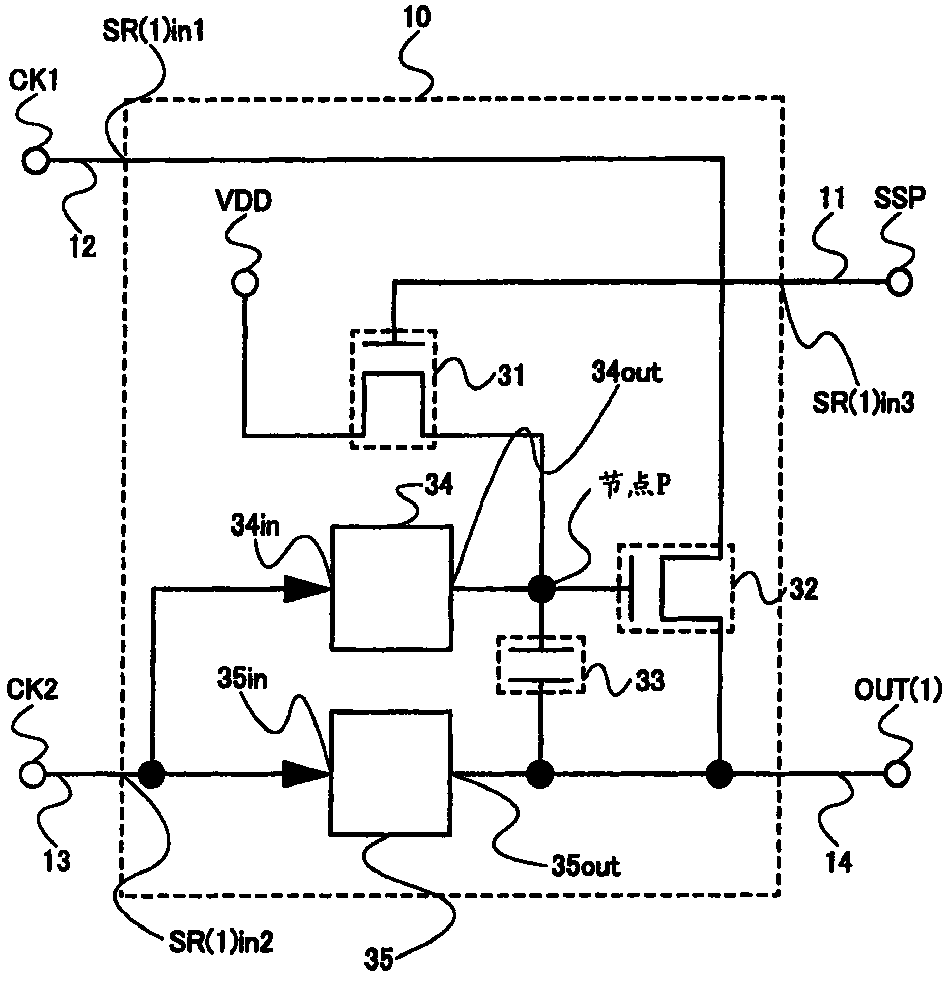
图3所示的电路10由输入端子11、输入端子12、输入端子13、输出端子14、晶体管31、晶体管32、电容器33、电路34和电路35构成。注意输入端子11到13连接到各个线。输入端子11到13和输出端子14同图1中描述的那些类似。晶体管31和32是由非晶半导体、多晶半导体或单晶半导体形成的n沟道晶体管。电容器33是具有两个电极的电容器。电路34是在CK2为高时向节点P输出低以及在CK2为低时其输出变为浮置状态的电路。电路35是在CK2为高时向输出端子14输出低以及在CK2为低时其输出变为浮置状态的电路。The
描述图3所示电路中的连接。晶体管31的栅极连接到输入端子11,其源极和漏极中的一个连接到VDD,并且源极和漏极中的另一个连接到电容器33的一个电极、晶体管32的栅极和电路34的输出端子,即节点P。此外,晶体管32的源极和漏极中的一个连接到输入端子12,且其源极和漏极中的另一个连接到电路35的输出端子、电容器33的另一个端子和输出端子14。输入端子13连接到电路34的输入端子和电路35的输入端子。Describe the connections in the circuit shown in Figure 3. The gate of the
参考图2中示出的该实施例模式的时序图,分别描述图3中示出的电路在周期T1、周期T2、和周期T3中的操作。而且,节点P和OUT(1)的电位在初始状态为VSS。Referring to the timing chart of this embodiment mode shown in FIG. 2, operations of the circuit shown in FIG. 3 in period T1, period T2, and period T3 are described respectively. Also, the potentials of the nodes P and OUT(1) are VSS in the initial state.
在周期T1中,SSP变为高,CK1变为低,CK2变为低,且CK3变为高。在这时晶体管31的栅极电位为VDD,其源极和漏极中的一个的电位为VDD,以及其源极和漏极中的另一个的电位为VSS。因此,晶体管31导通,并且节点P的电位开始上升。当节点P的电位变为比VDD低了晶体管31的阈值电压的电位时,节点P的电位的上升停止,由此晶体管31关断。在这时节点P的电位为Vn1。此外,当CK2为低时,电路34和35的输出处于浮置状态。因此,当电荷没有提供到节点P时,节点P变为浮置状态。在这时晶体管32的栅极电位是Vn1,其源极和漏极中的一个的电位为VSS,且其源极和漏极中的另一个为VSS,由此晶体管32导通。然而,当源极和漏极中的一个的电位和其另一个的电位相同时,没有电荷移动,由此没有电流流动和没有电位变化。电容器33保持作为输出端子14的电位的VSS和作为节点P的电位的Vn1之间的电位差。In period T1, SSP goes high, CK1 goes low, CK2 goes low, and CK3 goes high. At this time, the gate potential of the
在周期T2中,SSP变为低,CK1变为高,CK2变为低,且CK3变为低。在这时,晶体管31的栅极电位为VSS,其源极和漏极中的一个的电位为VDD,且其源极和漏极中的另一个的电位为Vn1,由此晶体管31关断。当CK2为低时,电路34和35的输出变为浮置状态。在这时晶体管32的栅极电位为Vn1,其源极和漏极中的一个的电位为VDD,且其源极和漏极中的另一个的电位,即输出端子14的电位变为VSS,由此晶体管32导通,并且输出端子14的电位开始上升。然后,连接在晶体管32的栅极和源极与漏极中的另一个之间的电容器33按照原状保持在周期T1中保持的电位差;因此,在源极和漏极中的另一个的电位上升时,栅电压同时上升。在这时节点P的电位为Vn2。当节点P的电位上升到与VDD和晶体管32的阈值电压的和一样高时,输出端子14的电位的上升停止在VDD,其与CK1相同。换句话说,通过自举操作,输出端子14的电位可以被提高得与VDD一样高,其是CK1的高电位。In period T2, SSP goes low, CK1 goes high, CK2 goes low, and CK3 goes low. At this time, the gate potential of the
在周期T3中,SSP为低,CK1为低,CK2为高,且CK3为低。在这时,当CK2为高并且从电路34输出VSS时,节点P的电位变为VSS,以及当从电路35输出VSS时,OUT(1)的电位变为VSS。在这时晶体管31的栅极电位变成VSS,源极和漏极中的一个的电位变为VDD,且其源极和漏极中的另一个的电位变为VSS,由此晶体管31关断。晶体管32的栅极电位变为VSS,其源极和漏极中的一个的电位变为VSS,且源极和漏极中的另一个的电位变为VSS,由此晶体管32关断。In period T3, SSP is low, CK1 is low, CK2 is high, and CK3 is low. At this time, when CK2 is high and VSS is output from the
通过上面描述的在周期T1、T2和T3中的操作,当在周期T1中输入SSP时,在周期T2中输出OUT(1)。即,通过连接n级电路10配置移位寄存器,其每一个输出具有时钟信号的周期的三分之一的移动的SSP。Through the above-described operations in periods T1, T2, and T3, when SSP is input in period T1, OUT(1) is output in period T2. That is, a shift register is configured by connecting n stages of
在图3中,示出了作为第一级的电路10的SR(1)。参考图51描述作为第n级的电路10的SR(n)。在图51中,晶体管31、晶体管32、电容器33、电路34、电路35、输入端子11、输入端子12、输入端子13和输出端子14同图3中示出的那些相似。从输入端子11输入的输入信号连接到前级的电路10的输出端子14。In FIG. 3 , SR(1) is shown as the
注意,晶体管31的栅极和晶体管32的源极和漏极中的另一个可以连接到用作电源线的线(下文称为“电源线”),例如,连接到例如正电源VDD和负电源VSS的电源线,另一电源线,或用作另一信号线的线(在下文中称为“信号线”)。而且,晶体管31的源极和漏极中的另一个可以连接到另外的信号线,例如,连接到例如CK1、CK2、CK3和SSP的信号线,另一信号线,或另一电源线。Note that the other of the gate of the
用于图3所示的移位寄存器电路的晶体管全部是n沟道晶体管,从而形成单极电路,然而,还可以仅使用p沟道晶体管。不必说,p沟道晶体管和n沟道晶体管可以组合使用。参考图55描述所有晶体管都是p沟道晶体管的移位寄存器电路。The transistors used for the shift register circuit shown in FIG. 3 are all n-channel transistors, forming a unipolar circuit, however, it is also possible to use only p-channel transistors. Needless to say, p-channel transistors and n-channel transistors may be used in combination. A shift register circuit in which all transistors are p-channel transistors will be described with reference to FIG. 55 .
在图55示出的电路结构中,正电源VDD、负电源VSS、输入端子11、输入端子12、输入端子13和输出端子14可以同图3中的那些相似。晶体管551和552是由非晶半导体、多晶半导体或单晶半导体形成的p沟道晶体管。电容器553具有两个电极。在CK2为低时电路554向节点P输出高,且在CK2为高时其输出变为浮置状态。在CK2为低时电路555向输出端子14输出高,且在CK2为高时其输出变为浮置状态。In the circuit structure shown in FIG. 55, the positive power supply VDD, the negative power supply VSS, the
描述图55中示出的电路的连接。晶体管551的栅极连接到输入端子11,其源极和漏极中的一个连接到正电源VSS,其源极和漏极中的另一个连接到电容器553的一个电极、晶体管552的栅极和电路554的输出端子,即节点P。晶体管552的源极和漏极中的一个连接到输入端子12,其源极和漏极中的另一个连接到电路555的输出端子、电容器553的另一个电极和输出端子14。输入端子13连接到电路554的输入端子和电路555的输入端子。The connection of the circuit shown in Fig. 55 is described. The gate of the
晶体管551的栅极和晶体管552的源极和漏极中的另一个可以连接到电源线,例如,连接到例如正电源VDD和负电源VSS的电源线,另一电源线,或另一信号线。此外,晶体管551的源极和漏极中的另一个可以连接到信号线,例如,连接到例如CK1、CK2、CK3和SSP的信号线,另一信号线,或另一电源线。The other of the gate of the
参考图59A描述图55中示出的电路554的结构实例。如图59A的电路554所示,输入端子13和节点P与图55中的那些类似。晶体管591是由非晶半导体、多晶半导体或单晶半导体形成的p沟道晶体管。A structural example of the
描述图59A中示出的电路的连接。晶体管591的栅极连接到输入端子13,其源极和漏极中的一个连接到VDD,且其源极和漏极中的另一个连接到节点P。The connection of the circuit shown in Fig. 59A is described. The gate of the
描述图59A的操作。当从输入端子13输入的CK2为低时晶体管591导通,由此VDD输出到节点P,而当CK2为高时晶体管591关断,由此向节点P什么也不输出。以这种方式,电路554具有在CK2为低时输出高以及在CK2为高时其输出变为浮置状态的功能。此外,可以使用具有相同功能的另一电路结构代替前面提到的电路结构。The operation of Fig. 59A is described. When CK2 input from the
注意,晶体管591的源极和漏极中的一个可以连接到信号线,例如,连接到例如CK1、CK2、CK3和SSP的信号线,另一信号线,或另一电源线。此外,晶体管591的栅极可以连接到电源线,例如,连接到例如正电源VDD和负电源VSS的电源线,另一电源线,或另一信号线。Note that one of the source and drain of the
参考图59B描述图55中示出的电路555的结构实例。如图59B的电路555所示,输入端子13和输出端子14与图55中的那些类似。晶体管592是由非晶半导体、多晶半导体或单晶半导体形成的p沟道晶体管。A structural example of the
描述图59B中示出的电路的操作。当从输入端子13输入的CK2为低时晶体管592导通,由此VDD输出到输出端子14,而当CK2为高时晶体管592关断,由此向输出端子14什么也不输出。以这种方式,电路555具有在CK2为低时输出高以及在CK2为高时其输出变为浮置状态的功能。此外,可以使用具有相同功能的另一电路结构代替前面提到的电路结构。The operation of the circuit shown in Fig. 59B is described. When CK2 input from the
注意,晶体管592的源极和漏极中的一个可以连接到信号线,例如,连接到例如CK1、CK2、CK3和SSP的信号线,另一信号线,或另一电源线。此外,晶体管592的栅极可以连接到电源线,例如,连接到例如正电源VDD和负电源VSS的电源线,另一电源线,或另一信号线。Note that one of the source and drain of the
接下来,参考图4A描述图3中示出的电路34的结构实例。Next, a structural example of the
在图4A示出的电路34中,输入端子13和节点P同图3中的那些类似。晶体管41是由非晶半导体、多晶半导体或单晶半导体形成的n沟道晶体管。In the
描述图4A示出的电路的连接。晶体管41的栅极连接到输入端子13,其源极和漏极中的一个连接到VSS,且其源极和漏极中的另一个连接到节点P。The connection of the circuit shown in FIG. 4A is described. The gate of the
描述图4A示出的电路的操作。当从输入端子13输入的CK2为高时晶体管41导通,由此VSS输出到节点P,而当CK2为低时晶体管41关断,由此向节点P什么也不输出。以这种方式,电路34具有在CK2为高时输出低以及在CK2为低时其输出变为浮置状态的功能。此外,可以使用具有相同功能的另一电路结构代替前面提到的电路结构。The operation of the circuit shown in FIG. 4A is described. The
注意,晶体管41的源极和漏极中的一个可以连接到信号线,例如,连接到例如CK1、CK2、CK3和SSP的信号线,另一信号线,或另一电源线。此外,晶体管41的栅极可以连接到电源线,例如,连接到例如正电源VDD和负电源VSS的电源线,另一电源线,或另一信号线。Note that one of the source and drain of the
参考图4B描述图3中示出的电路35的结构实例。A structural example of the
在图4B示出的电路35中,输入端子13和输出端子14同图3中的那些类似。晶体管42是由非晶半导体、多晶半导体或单晶半导体形成的n沟道晶体管。In the
描述图4B示出的电路的操作。当从输入端子13输入的CK2为高时晶体管42导通,由此VSS输出到输出端子14,而当CK2为低时晶体管42关断,由此向输出端子14什么也不输出。以这种方式,电路35具有在CK2为高时输出低以及在CK2为低时其输出变为浮置状态的功能。此外,可以使用具有相同功能的另一电路结构代替前面提到的电路结构。The operation of the circuit shown in FIG. 4B is described. When CK2 input from the
注意,晶体管42的源极和漏极中的一个可以连接到信号线,例如,连接到例如CK1、CK2、CK3和SSP的信号线,另一信号线,或另一电源线。不必说,晶体管42的源极和漏极中的一个可以连接到具有VSS的线,晶体管41的源极和漏极中的一个与其连接。此外,晶体管42的栅极可以连接到电源线,例如,连接到例如正电源VDD和负电源VSS的电源线,另一电源线,或另一信号线。Note that one of the source and drain of the
即,在图3和4示出的结构中,提供第一晶体管(晶体管31)、第二晶体管(晶体管32)、第三晶体管(晶体管41)和第四晶体管(晶体管42)。第一晶体管的源极和漏极中的一个连接到第一线(VDD),源极和漏极中的另一个连接到第二晶体管的栅电极和第三晶体管的源极和漏极中的另一个,第一晶体管的栅电极连接到第五线(输入端子11),第二晶体管的源极和漏极中的一个连接到第三线(输入端子12),源极和漏极中的另一个连接到第六线(输出端子14),第三晶体管的源极和漏极中的一个连接到第二线(VSS),其源极和漏极中的另一个连接到第二晶体管的栅电极,第三晶体管的栅电极连接到第四线(输入端子13),第四晶体管的源极和漏极中的一个连接到第二线(VSS),第四晶体管的源极和漏极中的另一个连接到第六线(输出端子14),以及其栅电极连接到第四线(输入端子13)。此外,第一晶体管的源极和漏极中的一个可以连接到第五线(输入端子11)。That is, in the structures shown in FIGS. 3 and 4 , a first transistor (transistor 31 ), a second transistor (transistor 32 ), a third transistor (transistor 41 ), and a fourth transistor (transistor 42 ) are provided. One of the source and drain of the first transistor is connected to the first line (VDD), and the other of the source and drain is connected to the gate electrode of the second transistor and the source and drain of the third transistor. In another, the gate electrode of the first transistor is connected to the fifth line (input terminal 11), one of the source and the drain of the second transistor is connected to the third line (input terminal 12), and the other of the source and the drain is connected to the third line (input terminal 12). One is connected to the sixth line (output terminal 14), one of the source and drain of the third transistor is connected to the second line (VSS), and the other of the source and drain is connected to the gate electrode of the second transistor , the gate electrode of the third transistor is connected to the fourth line (input terminal 13), one of the source and the drain of the fourth transistor is connected to the second line (VSS), and the other of the source and the drain of the fourth transistor is One is connected to the sixth line (output terminal 14), and its gate electrode is connected to the fourth line (input terminal 13). In addition, one of the source and the drain of the first transistor may be connected to the fifth line (input terminal 11).
在如上所述的移位寄存器电路中,当CK2变为高时,VSS可以施加到节点P和输出端子14。即,通过在非选择周期中每隔一定间隔输入VSS,可以降低噪声。而且,由于不存在固定导通的晶体管,因此可以抑制晶体管的特性退化。另外,由于至少四个晶体管可以用于操作,所以可以减少整个移位寄存器电路中的元件数目,这能够在绝缘衬底上的小区域内形成内部电路。In the shift register circuit as described above, VSS can be applied to node P and
下文描述的是该实施例模式的一些结构实例和操作实例,其是可变的。下面描述的结构实例和操作实例可以应用到“发明内容”、实施例模式和实施例。Described below are some structural examples and operational examples of this embodiment mode, which are variable. Structural examples and operation examples described below can be applied to "Summary of the Invention", Embodiment Modes, and Embodiments.
如图1所示,当电路10处于非选择周期中时,输入CK1、CK2和CK3的时钟信号,然而,可以提供开关元件等,以便在非选择周期中不向电路10输入这些时钟信号。结果,可以降低时钟信号线上的负荷,而且可以降低功耗。As shown in FIG. 1, when the
此外,在图1中,可以反向地扫描上面描述的移位寄存器电路。例如,第n级的电路10的输出可以输入到第(n-1)级的电路10。通过在所有级中重复这样,可以实现反向扫描。Furthermore, in FIG. 1, the above-described shift register circuit can be scanned in reverse. For example, the output of the
如图2所示,SSP、CK1、CK2和CK3的脉冲宽度是三分之一周期,该脉冲宽度可以比三分之一周期短一点。结果,可以抑制瞬时流动的电流,例如直通电流,并且可以实现具有高操作容限和低功耗的操作。在执行自举操作的电路结构中,存在处于浮置状态的节点,其有利于执行正常的自举操作。As shown in Fig. 2, the pulse width of SSP, CK1, CK2 and CK3 is one-third of the period, and the pulse width can be a little shorter than one-third of the period. As a result, instantaneously flowing current, such as a shoot-through current, can be suppressed, and operation with high operation margin and low power consumption can be realized. In a circuit configuration that performs a bootstrap operation, there are nodes in a floating state, which facilitate normal bootstrap operation.
在图2中,在SSP为高的周期中,CK3为具有相同脉冲宽度的高。然而,本发明不限于此。例如,当信号从外部电路传送到内部电路时,根据缓冲电路、改变信号幅度的电平转移电路等,延迟时间可以在控制信号之间变化。In Figure 2, during the period that SSP is high, CK3 is high with the same pulse width. However, the present invention is not limited thereto. For example, when a signal is transferred from an external circuit to an internal circuit, the delay time can vary between control signals according to a buffer circuit, a level shift circuit that changes the signal amplitude, and the like.
在图3中,连接电容器33用于自举操作。然而,如果在晶体管32的栅极以及源极和漏极中的另一个之间存在栅-源电容等,其大得足以用于自举操作,那么不总是需要提供电容器33。而且,可以通过任何方法形成电容器33。例如,可以在半导体层和栅极布线层之间或在非晶半导体层和线之间形成电容器。有利的是在半导体层和栅极布线层之间形成电容器,因为不论底栅晶体管或顶栅晶体管,可以用插入其间的薄GI膜(栅极绝缘膜)形成电容器,这能够以较小的区域获得更大的电容。In FIG. 3, a
在图3中,SSP输入到晶体管31的栅极,然而,其栅极以及源极和漏极中的一个可以彼此连接,对其可以输入SSP。结果,由于不需要正电源VDD,所以可以减少一个电源线。因此,用来形成移位寄存器电路的区域可以更小。从而,可以提供具有更高分辨率和更窄框架的显示器件。In FIG. 3 , the SSP is input to the gate of the
图3示出的电路34和35可以是如上面描述的在CK2为高时输出VSS以及在CK2为低时其输出变为浮置状态的任何电路。而且,下一级的电路10的输出可以输入到电路34的输入端子,后一级的电路10的输出可以类似地输入到电路35的输入端子,或后一级的电路10的输出可以输入到电路34和35的输入端子。通过利用后一级的电路10的输出,可以使电路34和35不仅和控制信号同步,还和移位寄存器电路的实际输出也同步;因此,优点是可以根据该移位寄存器电路的操作适当改变电位。
如图3所示,电容器可以连接在节点P和VSS或VDD之间。通过连接电容器,可以稳定节点P的电位。As shown in FIG. 3, a capacitor may be connected between node P and VSS or VDD. By connecting a capacitor, the potential of the node P can be stabilized.
注意,在图3中不总是需要电路34。即,当通过电路35每隔一定间隔输出VSS时,即使在节点P具有噪声时,晶体管32也将关断。结果,可以减少元件的数量。在那时,电容器可以连接在节点P和VSS或VDD之间。Note that
[实施例模式2][Embodiment Mode 2]
在该实施例模式中,参考图2和5到7描述移位寄存器电路的结构和操作,其中通过每隔一定间隔输出VSS,降低了在非选择周期中输出电压的噪声。In this embodiment mode, the structure and operation of the shift register circuit in which the noise of the output voltage in the non-selection period is reduced by outputting VSS at regular intervals is described with reference to FIGS. 2 and 5 to 7 .
如图5所示,电路50借助串联连接的n个(n为2或更大的自然数)电路SR(1)到SR(n)形成移位寄存器电路。As shown in FIG. 5, the
输入端子51是用来在作为第一级的电路50的SR(1)中输入起始脉冲和用来在作为第二到第n级的电路50的SR(2)中输入来自前级的输出端子55的输出的输入端子。输入端子52是用于以CK1作为时钟信号输入给作为第一级的电路50的SR(1)、CK2作为时钟信号输入给作为第二级的电路50的SR(2)、CK3作为时钟信号输入给作为第三级的电路50的SR(3)、以及CK1输入给作为第四级的电路50的SR(4)的这种方式,来顺序输入CK1、CK2和CK3的输入端子。输入端子53是用于以CK2输入给作为第一级的电路50的SR(1)、CK3输入给作为第二级的电路50的SR(2)、CK1输入给作为第三级的电路50的SR(3)、以及CK2输入给作为第四级的电路50的SR(4)的这种方式,来顺序输入时钟信号的输入端子。输入端子54是用于以CK3输入给作为第一级的电路50的SR(1)、CK1输入给作为第二级的电路50的SR(2)、CK2输入给作为第三级的电路50的SR(3)、以及CK3输入给作为第四级的电路50的SR(4)的这种方式,来顺序输入时钟信号的输入端子。输出端子55是电路50的输出端子,其从作为第一级的电路50的SR(1)输出OUT(1)并向作为第二级的电路50的SR(2)的输入端子51输出OUT(1),从作为第二级的电路50的SR(2)输出OUT(2)并向作为第三级的电路50的SR(3)的输入端子51输出OUT(2)。The
这里,SSP、CK1、CK2和CK3是每个都具有高和低的二进制值的1位信号。高是与正电源VDD相同的电位,而低是与负电源VSS相同的电位。这里,SSP、CK1、CK2和CK3是每个都具有高和低的二进制值的1位信号。而且,OUT(1)、OUT(2)、OUT(3)、OUT(n-1)和OUT(n)是每个都具有二进制值的1位信号。高是与正电源VDD相同的电位,而低是与负电源VSS相同的电位。Here, SSP, CK1, CK2, and CK3 are 1-bit signals each having binary values of high and low. High is the same potential as the positive power supply VDD, and Low is the same potential as the negative power supply VSS. Here, SSP, CK1, CK2, and CK3 are 1-bit signals each having binary values of high and low. Also, OUT(1), OUT(2), OUT(3), OUT(n-1), and OUT(n) are 1-bit signals each having a binary value. High is the same potential as the positive power supply VDD, and Low is the same potential as the negative power supply VSS.
参考图2示出的该实施例模式的时序图,描述图5示出的移位寄存器电路的操作。Referring to the timing chart of this embodiment mode shown in FIG. 2, the operation of the shift register circuit shown in FIG. 5 will be described.
SSP、CK1、CK2和CK3可以与实施例模式1中的那些类似。注意,节点P(1)是与后面描述的图6中的节点P相同的电位。OUT(1)是作为第一级的电路50的SR(1)的输出,OUT(2)是作为第二级的电路50的SR(2)的输出,OUT(3)是作为第三级的电路50的SR(3)的输出,OUT(n-1)是作为第n-1级的电路50的SR(n-1)的输出,以及OUT(n)是作为第n级的电路50的SR(n)的输出。SSP, CK1, CK2, and CK3 may be similar to those in
在图2的时序图中,当在周期T1中SSP如所示变成高时,在周期T2中OUT(1)如所示变成高,并且在周期T3中OUT(2)如所示变成高。用这种方式,通过移动SSP的输出实现移位寄存器电路。In the timing diagram of Figure 2, when SSP goes high as shown in period T1, OUT(1) goes high as shown in period T2, and OUT(2) goes high as shown in period T3 into high. In this way, a shift register circuit is implemented by shifting the output of the SSP.
接下来,参考图6描述第一级的电路50的结构。Next, the structure of the
图6所示的电路50利用输入端子51、输入端子52、输入端子53、输入端子54、输出端子55、晶体管31、晶体管32、电容器33、电路34和电路35来配置。输入端子51、输入端子52、输入端子53、输入端子54和输出端子55类似于图5中描述的那些。晶体管31和晶体管32类似于图3中示出的那些。电路61具有在CK2为高时向节点P输出低和在CK2为低时其输出变为浮置状态的功能。电路62具有在CK2或CK3中的任一个为高时向输出端子55输出低和在CK2和CK3为低时其输出变为浮置状态的功能。The
对图6所示电路的连接进行描述。晶体管31的栅极连接到输入端子51,其源极和漏极中的一个连接到VDD,并且其源极和漏极中的另一个连接到电容器33的一个电极、晶体管32的栅极和电路61的输出端子,即连接到节点P。晶体管32的源极和漏极中的一个连接到输入端子52,且其源极和漏极中的另一个连接到电路62的输出端子、电容器33的另一个电极和输出端子55。输入端子53连接到电路61的输入端子和电路62的输入端子。输入端子54连接到电路62的输入端子。The connection of the circuit shown in Fig. 6 will be described. The gate of the
参考图2中示出的该实施例模式的时序图,分别描述图6中示出的电路在周期T1、周期T2和周期T3中的操作。而且,节点P和OUT(1)的电位在初始状态为VSS。Referring to the timing chart of this embodiment mode shown in FIG. 2, operations of the circuit shown in FIG. 6 in period T1, period T2, and period T3 are described respectively. Also, the potentials of the nodes P and OUT(1) are VSS in the initial state.
在周期T1中,SSP变为高,CK1变为低,CK2变为低,且CK3变为高。在这时晶体管31的栅极电位为VDD,其源极和漏极中的一个的电位为VDD,以及其源极和漏极中的另一个的电位为VSS。因此,晶体管31导通,并且节点P的电位开始从VSS上升。当节点P的电位变为比VDD低了晶体管31的阈值电压的电位时,节点P的电位停止上升,由此晶体管31关断。在这时节点P的电位为Vn1。此外,当CK2为低时,电路61的输出处于浮置状态。因此,当电荷没有施加到节点P时,所以节点P变为浮置状态。当CK2为低且CK3为高时,电路62输出低。在这时晶体管32的栅极电位是Vn1,其源极和漏极中的一个的电位为VSS,且其源极和漏极中的另一个为VSS,这样晶体管32导通。然而,当源极和漏极中的一个的电位和其另一个的电位相同时,没有电荷移动,由此没有电流流动和没有电位变化。电容器33保持作为输出端子55的电位的VSS和作为节点P的电位的Vn1之间的电位差。In period T1, SSP goes high, CK1 goes low, CK2 goes low, and CK3 goes high. At this time, the gate potential of the
在周期T2中,SSP变为低,CK1变为高,CK2变为低,且CK3变为低。在这时,晶体管31的栅极电位为VSS,其源极和漏极中的一个的电位为VDD,且其源极和漏极中的另一个的电位为Vn1,由此晶体管31关断。当CK2为低时,电路61的输出变为浮置状态。当CK2为低且CK3为低时,电路62的输出变为浮置状态。在这时晶体管32的栅极电位为Vn1,其源极和漏极中的一个的电位为VDD,且其源极和漏极中的另一个的电位,即输出端子55的电位变为VSS,由此晶体管32导通,并且输出端子55的电位开始上升。然后,连接在晶体管32的栅极以及源极和漏极中的另一个之间的电容器33按照原状保持在周期T1中保持的电位差;因此,在源极和漏极中的另一个的电位上升时,栅电压同时上升。在这时节点P的电位为Vn2。当节点P的电位上升得与VDD和晶体管32的阈值电压的和一样高时,输出端子14的电位的上升停止在VDD,其与CK1相同。换句话说,通过自举操作,输出端子55的电位可以被提高得与CK1的高电位VDD一样高。In period T2, SSP goes low, CK1 goes high, CK2 goes low, and CK3 goes low. At this time, the gate potential of the
在周期T3中,SSP为低,CK1为低,CK2为高,且CK3为低。在这时,当CK2为高并且从电路61输出VSS时,节点P的电位变为VSS,以及当从电路62输出VSS时,OUT(1)的电位变为VSS。在这时晶体管31的栅极电位变为VSS,源极和漏极中的一个的电位变为VDD,且其源极和漏极中的另一个的电位变为VSS,由此晶体管31关断。晶体管32的栅极电位变为VSS,其源极和漏极中的一个的电位变为VSS,且源极和漏极中的另一个的电位变为VSS,由此晶体管32关断。In period T3, SSP is low, CK1 is low, CK2 is high, and CK3 is low. At this time, when CK2 is high and VSS is output from the
通过上面描述的在周期T1、T2和T3中的操作,当在周期T1中输入SSP时,在周期T2中输出OUT(1)。即,通过连接n级电路50配置移位寄存器电路,其每一个输出时钟信号的周期的三分之一的移动的SSP。Through the above-described operations in periods T1, T2, and T3, when SSP is input in period T1, OUT(1) is output in period T2. That is, a shift register circuit is configured by connecting n stages of
虽然已描述了图6示出的第一级的电路50,但是现在参考图52描述第n级的电路50。在图52中,晶体管31、晶体管32、电容器33、电路61、电路62、输入端子51、输入端子52、输入端子53、输入端子54和输出端子55同图6中描述的那些相似。该电路的特点是,从输入端子51输入的输入信号连接到前级的电路的输出端子55。Although the
注意,晶体管31的栅极和晶体管32的源极和漏极中的另一个可以连接到电源线,例如,连接到例如正电源VDD和负电源VSS的电源线,另一电源线,或另一信号线。而且,晶体管31的源极和漏极中的另一个可以连接到信号线,例如,连接到例如CK1、CK2、CK3和SSP的信号线,另一信号线,或另一电源线。Note that the other of the gate of the
用于图6所示的移位寄存器电路的晶体管全部是n沟道晶体管,从而形成单极电路,然而,也可以仅使用p沟道晶体管。不必说,p沟道晶体管和n沟道晶体管可以组合使用。参考图56描述所有晶体管都是p沟道晶体管的移位寄存器电路。The transistors used for the shift register circuit shown in FIG. 6 are all n-channel transistors, forming a unipolar circuit, however, only p-channel transistors may also be used. Needless to say, p-channel transistors and n-channel transistors may be used in combination. A shift register circuit in which all transistors are p-channel transistors will be described with reference to FIG. 56 .
在图56示出的电路结构中,正电源VDD、负电源VSS、输入端子51、输入端子52、输入端子53、输入端子54、晶体管551、晶体管552和电容器553可以同图55中的那些相似。电路561具有在CK2为低时向节点P输出高和在CK2为高时其输出变为浮置状态的功能。电路562具有在CK2或CK3中的任一个为低时向节点P输出高和在CK2和CK3为高时其输出变为浮置状态的功能。In the circuit structure shown in FIG. 56, the positive power supply VDD, the negative power supply VSS, the
描述图56中示出的电路的连接。晶体管551的栅极连接到输入端子51,其源极和漏极中的一个连接到正电源VSS,以及其源极和漏极中的另一个连接到电容器553的一个电极、晶体管552的栅极和电路561的输出端子,即连接到节点P。晶体管552的源极和漏极中的一个连接到输入端子52,以及其源极和漏极中的另一个连接到电路562的输出端子、电容器553的另一个电极和输出端子55。输入端子53连接到电路561的输入端子和电路562的第一输入端子。输入端子54连接到电路562中的第一晶体管的第二输入端子。The connection of the circuit shown in Fig. 56 is described. The gate of the
注意,晶体管551的栅极和晶体管552的源极和漏极中的另一个可以连接到电源线,例如,连接到例如正电源VDD和负电源VSS的电源线,另一电源线,或另一信号线。此外,晶体管551的源极和漏极中的另一个可以连接到信号线,例如,连接到例如CK1、CK2、CK3和SSP的信号线,另一信号线,或另一电源线。Note that the other of the gate of the
接下来,参考图60A描述图56中示出的电路561的结构实例。Next, a structural example of the
图60A示出的电路561中的输入端子53和节点P与图55中的那些类似。晶体管601是由非晶半导体、多晶半导体或单晶半导体形成的p沟道晶体管。The
描述图60A中示出的电路的连接。晶体管601的栅极连接到输入端子53,其源极和漏极中的一个连接到VDD,且其源极和漏极中的另一个连接到节点P。The connection of the circuit shown in Fig. 60A is described. The gate of the
描述图60A示出的电路的操作。当从输入端子53输入的CK2为低时晶体管601导通,由此VDD输出到节点P,而当CK2为高时晶体管601关断,由此向节点P什么也不输出。以这种方式,电路561具有在CK2为低时输出高和在CK2为高时其输出变为浮置状态的功能。此外,可以使用具有相同功能的另一电路结构代替前面提到的电路结构。The operation of the circuit shown in Fig. 60A is described. When CK2 input from the
注意,晶体管601的源极和漏极中的一个可以连接到信号线,例如,连接到例如CK1、CK2、CK3和SSP的信号线,另一信号线,或另一电源线。此外,晶体管601的栅极可以连接到电源线,例如,连接到例如正电源VDD和负电源VSS的电源线,另一电源线,或另一信号线。Note that one of the source and drain of the
参考图60B描述图56中示出的电路562的结构实例。A structural example of the
在图60B所示的电路562中,输入端子53和54以及输出端子55与图55中的那些类似。晶体管602和603是由非晶半导体、多晶半导体或单晶半导体形成的p沟道晶体管。In a
描述图60B中示出的电路的操作。当从输入端子53输入的CK2为低时晶体管602导通,由此VDD输出到输出端子55,而当CK2为高时晶体管602关断,由此向输出端子55什么也不输出。当从输入端子54输入的CK3为低时晶体管603导通,由此VDD输出到输出端子55,而当CK3为高时向输出端子55什么也不输出。以这种方式,电路562具有在CK2和CK3为低时输出高以及在CK2和CK3为高时其输出变为浮置状态的功能。此外,可以使用具有相同功能的另一电路结构代替前面提到的电路结构。The operation of the circuit shown in Fig. 60B is described. When CK2 input from the
注意,晶体管592的源极和漏极中的一个可以连接到信号线,例如,连接到例如CK1、CK2、CK3和SSP的信号线,另一信号线,或另一电源线。此外,晶体管592的栅极可以连接到电源线,例如,连接到例如正电源VDD和负电源VSS的电源线,另一电源线,或另一信号线。Note that one of the source and drain of the
接下来,参考图7A描述图6中示出的电路61的结构实例。Next, a structural example of the
如图7A示出的电路61所示,输入端子53和节点P同图6中的那些类似。晶体管71是由非晶半导体、多晶半导体或单晶半导体形成的n沟道晶体管。As shown in
描述图7A示出的电路的连接。晶体管71的栅极连接到输入端子53,其源极和漏极中的一个连接到VSS,且源极和漏极中的另一个连接到节点P。The connection of the circuit shown in Fig. 7A is described. The gate of the
描述图7A示出的电路的操作。当从输入端子53输入的CK2为高时晶体管71导通,由此VSS输出到节点P,而当CK2为低时晶体管71关断,由此向节点P什么也不输出。以这种方式,电路71具有在CK2为高时输出低和在CK2为低时其输出变为浮置状态的功能。此外,可以使用具有相同功能的另一电路结构代替前面提到的电路结构。The operation of the circuit shown in FIG. 7A is described. When CK2 input from the
晶体管71的源极和漏极中的一个可以连接到信号线,例如,连接到例如CK1、CK2、CK3和SSP的信号线,另一信号线,或另一电源线。晶体管71的栅极可以连接到电源线,例如,连接到例如正电源VDD和负电源VSS的电源线,另一电源线,或另一信号线。One of the source and the drain of the
参考图7B描述图6中示出的电路62的结构实例。A structural example of the
如图7B示出的电路62所示,输入端子53、输入端子54和OUT(1)同图6中的那些类似。晶体管72和73是由非晶半导体、多晶半导体或单晶半导体形成的n沟道晶体管。As shown in
描述图7B示出的电路的连接。晶体管72的栅极连接到输入端子53,其源极和漏极中的一个连接到VSS,且其源极和漏极中的另一个连接到输出端子55。晶体管73的栅极连接到输入端子54,其源极和漏极中的一个连接到VSS,且源极和漏极中的另一个连接到输出端子55。不必说,晶体管72和73的源极和漏极中的一个可以连接到具有VSS的线,晶体管71的源极和漏极中的一个与其连接。The connection of the circuit shown in FIG. 7B is described. The gate of the
描述图7B示出的电路的操作。当从输入端子53输入的CK2为高时晶体管72导通,由此VSS输出到OUT(1),而当CK2为低时晶体管72关断,由此向OUT(1)什么也不输出。当从输入端子54输入的CK3为高时晶体管73导通,由此VSS输出到OUT(1),而当CK3为低时晶体管73关断,由此向OUT(1)什么也不输出。以这种方式,电路62具有在CK2或CK3中的任一个为高时向OUT(1)输出低以及在CK2和CK3为低时其输出变为浮置状态的功能。此外,可以使用具有相同功能的另一电路结构代替前面提到的电路结构。The operation of the circuit shown in FIG. 7B is described. The
注意,晶体管72和晶体管73中的每一个的源极和漏极中的一个可以连接到信号线,例如,连接到例如CK1、CK2、CK3和SSP的信号线,另一信号线,或另一电源线。此外,晶体管72的栅极可以连接到电源线,例如,连接到例如正电源VDD和负电源VSS的电源线,另一电源线,或另一信号线。晶体管73的栅极可以连接到电源线,例如,连接到例如正电源VDD和负电源VSS的电源线,另一电源线,或另一信号线。Note that one of the source and drain of each of the
即,在图6和7示出的结构中,提供第一晶体管(晶体管31)、第二晶体管(晶体管32)、第三晶体管(晶体管71)、第四晶体管(晶体管72)和第五晶体管(晶体管73)。第一晶体管的源极和漏极中的一个连接到第一线(VDD),源极和漏极中的另一个连接到第二晶体管的栅电极和第三晶体管的源极和漏极中的另一个,第一晶体管的栅电极连接到第五线(输入端子51),第二晶体管的源极和漏极中的一个连接到第三线(输入端子52),源极和漏极中的另一个连接到第六线(输出端子55),第三晶体管的源极和漏极中的一个连接到第二线(VSS),其源极和漏极中的另一个连接到第二晶体管的栅电极,第三晶体管的栅电极连接到第四线(输入端子53),第四晶体管的源极和漏极中的一个连接到第二线(VSS),第四晶体管的源极和漏极中的另一个连接到第六线(输出端子55),以及其栅电极连接到第四线(输入端子53),第五晶体管的源极和漏极中的一个连接到第二线(VSS),其源极和漏极中的另一个连接到第六线(输出端子55),且其栅电极连接到第七线(输入端子54)。此外,第一晶体管的源极和漏极中的一个可以连接到第五线(输入端子51)。That is, in the structures shown in FIGS. 6 and 7, a first transistor (transistor 31), a second transistor (transistor 32), a third transistor (transistor 71), a fourth transistor (transistor 72), and a fifth transistor (transistor 72) are provided. transistor 73). One of the source and drain of the first transistor is connected to the first line (VDD), and the other of the source and drain is connected to the gate electrode of the second transistor and the source and drain of the third transistor. In another, the gate electrode of the first transistor is connected to the fifth line (input terminal 51), one of the source and the drain of the second transistor is connected to the third line (input terminal 52), and the other of the source and the drain is connected to the third line (input terminal 52). One is connected to the sixth line (output terminal 55), one of the source and drain of the third transistor is connected to the second line (VSS), and the other of the source and drain is connected to the gate electrode of the second transistor , the gate electrode of the third transistor is connected to the fourth line (input terminal 53), one of the source and the drain of the fourth transistor is connected to the second line (VSS), and the other of the source and the drain of the fourth transistor is One is connected to the sixth line (output terminal 55), and its gate electrode is connected to the fourth line (input terminal 53), one of the source and drain of the fifth transistor is connected to the second line (VSS), and its source The other of the drain and the drain is connected to the sixth line (output terminal 55 ), and its gate electrode is connected to the seventh line (input terminal 54 ). Also, one of the source and the drain of the first transistor may be connected to the fifth line (input terminal 51).
在如上所述的移位寄存器电路中,当CK2或CK3中的任一个变为高时,VSS可以施加到输出端子55。即,通过在非选择周期中每隔一定间隔输入VSS,可以降低噪声。而且,由于不存在固定导通的晶体管,所以可以抑制晶体管的特性退化。另外,如在非选择周期中所示的,与实施例模式1相比,可以向输出端子55提供VSS两倍周期长。因此,可以进一步抑制噪声。In the shift register circuit as described above, when either of CK2 or CK3 goes high, VSS can be applied to the
下文描述的是该实施例模式的一些结构实例和操作实例,其是可变的。下面描述的结构实例和操作实例可以应用到“发明内容”、实施例模式和实施例。在实施例模式1中描述的结构实例和操作实例可以应用到该实施例模式。Described below are some structural examples and operational examples of this embodiment mode, which are variable. Structural examples and operation examples described below can be applied to "Summary of the Invention", Embodiment Modes, and Embodiments. The structural example and operation example described in
如图6所示,可以在节点P和VSS或VDD之间提供电容器。通过连接电容器,可以稳定节点P的电位。As shown in FIG. 6, a capacitor may be provided between node P and VSS or VDD. By connecting a capacitor, the potential of the node P can be stabilized.
在图6中,连接电容器33用于自举操作。然而,如果在晶体管32的栅极以及源极和漏极中的另一个之间存在电容等,其大得足以用于自举操作,那么不总是需要提供电容器33。而且,可以在任何地方形成电容器33。例如,可以在非晶半导体层和栅极布线层之间或在非晶半导体层和线之间形成电容器。有利的是在半导体层和栅极布线层之间形成电容器,因为不论底栅晶体管或顶栅晶体管,可以用插入其间的薄GI膜(栅极绝缘膜)形成电容器,这能够以较小的区域获得更大的电容。In FIG. 6, a
注意,在图6中电路61不总是被需要的。即,当通过电路62每隔一定间隔输出VSS时,晶体管32将关断,即使在节点P具有噪声时。结果,可以减少元件的数量。在那时,电容器可以连接在节点P和VSS或VDD之间。Note that
一个级的电路50的输出可以输入到电路62的输入端子,后一级的电路50的输出可以类似地输入到电路35的输入端子,或后一级的电路50的输出可以输入到电路61和62的输入端子。通过利用后一级的电路50的输出,可以使信号不仅和控制信号同步,还和移位寄存器的实际输出也同步;因此,优点是可以根据该移位寄存器电路的操作改变电位。The output of the
如图6所示,电容器可以连接在节点P和VSS或VDD之间。通过连接电容器,可以稳定节点P的电位。As shown in FIG. 6, a capacitor may be connected between node P and VSS or VDD. By connecting a capacitor, the potential of the node P can be stabilized.
[实施例模式3][Embodiment Mode 3]
在该实施例模式中,参考图2、5、以及8到10描述移位寄存器电路的结构和操作,其中通过在非选择周期中输出VSS,降低了在非选择周期中的输出电压的噪声。In this embodiment mode, the structure and operation of the shift register circuit in which the noise of the output voltage in the non-selection period is reduced by outputting VSS in the non-selection period is described with reference to FIGS. 2 , 5 , and 8 to 10 .
图5示出的移位寄存器电路的结构和其操作与实施例模式2中描述的那些相似。The structure of the shift register circuit shown in FIG. 5 and its operation are similar to those described in
参考图8描述作为第一级的电路50的SR(1)的结构。图8所示的电路50利用输入端子51、输入端子52、输入端子53、输入端子54、输出端子55、晶体管31、晶体管32、电容器33、电路81、电路82和电路83来配置。The structure of SR(1) as the
输入端子51、输入端子52、输入端子53、输入端子54、输出端子55、晶体管31、晶体管32和电容器33类似于图5中示出的那些。The
电路81具有在CK2为高时向节点P输出低以及在CK2为低时其输出变为浮置状态的功能。电路82具有在电路83的输出为高且CK1、CK2和CK3中的任何一个为高时向输出端子55输出低以及在CK1、CK2和CK3为低时其输出变为浮置状态的功能。电路83具有在节点P的电位大约为VDD或等于或高于VDD时向电路82输出低以及在节点P的电位为VSS时向电路82输出高的功能。
对图8所示电路的连接进行描述。晶体管31的栅极连接到输入端子51,其源极和漏极中的一个连接到VDD,并且源极和漏极中的另一个连接到电容器33的一个电极、晶体管32的栅极、电路83的输入端子和电路81的输出端子,即连接到节点P。晶体管32的源极和漏极中的一个连接到输入端子52,源极和漏极中的另一个连接到电路82的输出端子、电容器33的另一个端子和输出端子55。输入端子52连接到电路82的输入端子,输入端子53连接到电路81的输入端子和电路82的输入端子。输入端子54连接到电路82的输入端子。电路83的输出端子连接到电路82的输入端子。The connection of the circuit shown in Fig. 8 will be described. The gate of the
参考图2中示出的该实施例模式的时序图,分别描述图8中示出的电路在周期T1、周期T2和周期T3中的操作。而且,节点P和OUT(1)的电位在初始状态为VSS。Referring to the timing chart of this embodiment mode shown in FIG. 2, operations of the circuit shown in FIG. 8 in period T1, period T2, and period T3 are described respectively. Also, the potentials of the nodes P and OUT(1) are VSS in the initial state.
在周期T1中,SSP变为高,CK1变为低,CK2变为低,且CK3变为高。在这时晶体管31的栅极电位为VDD,其源极和漏极中的一个的电位为VDD,以及其源极和漏极中的另一个的电位为VSS。因此,晶体管31导通,并且节点P的电位开始从VSS上升。当节点P的电位变为比VDD低了晶体管31的阈值电压的电位时,节点P的电位停止上升,由此晶体管31关断。在这时节点P的电位为Vn1。此外,当CK2为低时,电路81的输出处于浮置状态。因此,当电荷没有提供到节点P时,节点P变为浮置状态。当电路83输出低,CK1为低,CK2为低,且CK3为高时,电路82输出低。在这时晶体管32的栅极电位是Vn1,其源极和漏极中的一个的电位为VSS,且其源极和漏极中的另一个为VSS,这样晶体管32导通。然而,当源极和漏极中的一个的电位和其另一个的电位相同时,没有电荷移动,由此没有电流流动和没有电位变化。电容器33保持作为输出端子55的电位的VSS和作为节点P的电位的Vn1之间的电位差。In period T1, SSP goes high, CK1 goes low, CK2 goes low, and CK3 goes high. At this time, the gate potential of the
在周期T2中,SSP变为低,CK1变为高,CK2变为低,且CK3变为低。在这时,晶体管31的栅极电位为VSS,其源极和漏极中的一个的电位为VDD,且其源极和漏极中的另一个的电位为Vn1,由此晶体管31关断。当CK2为低时,电路61的输出变为浮置状态。当节点P的电位为Vn1时,电路83向电路82的输入端子输出低。当电路83的输出为低,CK1为高,CK2为低,且CK3为低时,电路82的输出变为浮置状态。在这时晶体管32的栅极电位为Vn1,其源极和漏极中的一个的电位为VDD,且其源极和漏极中的另一个的电位,即输出端子55的电位变为VSS,由此晶体管32导通,并且输出端子55的电位开始上升。然后,连接在晶体管32的栅极以及源极和漏极中的另一个之间的电容器33按照原状保持在周期T1中保持的电位差;因此,在源极和漏极中的另一个的电位上升时,栅电压同时上升。在这时节点P的电位为Vn2。当节点P的电位上升得与VDD和晶体管32的阈值电压的和一样高时,输出端子55的电位的上升停止在VDD,其与CK1相同。换句话说,通过自举操作,输出端子55的电位可以被提高得与CK1的高电位VDD一样高。In period T2, SSP goes low, CK1 goes high, CK2 goes low, and CK3 goes low. At this time, the gate potential of the
在周期T3中,SSP为低,CK1为低,CK2为高,且CK3为低。在这时,当CK2为高并且从电路81输出VSS时,节点P的电位变为VSS,由此电路83向电路82的输入端子输出高。当从电路82输出VSS时,OUT(1)的电位变为VSS。在这时晶体管31的栅极电位变为VSS,源极和漏极中的一个的电位变为VDD,且其源极和漏极中的另一个的电位变为VSS,由此晶体管31关断。晶体管32的栅极电位变为VSS,其源极和漏极中的一个的电位变为VSS,且源极和漏极中的另一个的电位变为VSS,由此晶体管32关断。In period T3, SSP is low, CK1 is low, CK2 is high, and CK3 is low. At this time, when CK2 is high and VSS is output from the
通过上面描述的在周期T1、T2和T3中的操作,当在周期T1中输入SSP时,在周期T2中输出OUT(1)。即,通过连接n级电路50配置移位寄存器,其每一个输出具有时钟信号的周期的三分之一的移动的SSP。Through the above-described operations in periods T1, T2, and T3, when SSP is input in period T1, OUT(1) is output in period T2. That is, the shift register is configured by connecting n stages of
虽然已描述了图8示出的第一级的电路50,但是现在参考图53描述第n级的电路。Although the
在图53中,晶体管31和32,电容器33,电路81、82和83,输入端子51、52、53和54,以及输出端子55同图8中示出的那些相似。该电路的特点是,从输入端子51输入的输入信号连接到前级的电路的输出端子55。In FIG. 53,
用于图8所示的移位寄存器电路的晶体管全部是n沟道晶体管,从而形成单极电路,然而,也可以仅使用p沟道晶体管。不必说,p沟道晶体管和n沟道晶体管可以组合使用。参考图57描述所有晶体管都是p沟道晶体管的移位寄存器电路。The transistors used for the shift register circuit shown in FIG. 8 are all n-channel transistors, thereby forming a unipolar circuit, however, only p-channel transistors may also be used. Needless to say, p-channel transistors and n-channel transistors may be used in combination. A shift register circuit in which all transistors are p-channel transistors will be described with reference to FIG. 57 .
在图57示出的电路结构中,正电源VDD、负电源VSS、输入端子51、输入端子52、输入端子53、输入端子54、晶体管551、晶体管552和电容器553可以同图55中的那些相似。电路571具有在CK2为低时向节点P输出高和在CK2为高时其输出变为浮置状态的功能。电路572在CK1、CK2和CK3中的任何一个为低时向输出端子55输出高。In the circuit structure shown in FIG. 57, the positive power supply VDD, the negative power supply VSS, the
描述图57中示出的电路的连接。晶体管551的栅极连接到输入端子51,其源极和漏极中的一个连接到正电源VSS,其源极和漏极中的另一个连接到电容器553的一个电极、晶体管552的栅极和电路571的输出端子,即连接到节点P。晶体管552的源极和漏极中的一个连接到输入端子52,其源极和漏极中的另一个连接到电路572的输出端子、电容器553的另一个电极和输出端子55。输入端子52连接到电路572的输入端子。输入端子53连接到电路571的输入端子和电路572的第一输入端子。输入端子54连接到电路572中的第一晶体管的第二输入端子。The connection of the circuit shown in Fig. 57 is described. The gate of the
注意,晶体管551的栅极和晶体管552的源极和漏极中的另一个可以连接到电源线,例如,连接到例如正电源VDD和负电源VSS的电源线,另一电源线,或另一信号线。此外,晶体管551的源极和漏极中的另一个可以连接到信号线,例如,连接到例如CK1、CK2、CK3和SSP的信号线,另一信号线,或另一电源线。Note that the other of the gate of the
接下来,参考图9A描述图8中示出的电路81结构实例。Next, a structural example of the
在图9A示出的电路81中,输入端子53和节点P与图8中的那些类似。晶体管91是由非晶半导体、多晶半导体或单晶半导体形成的n沟道晶体管。In the
描述图9A中示出的电路的连接。晶体管91的栅极连接到输入端子53,其源极和漏极中的一个连接到VSS,且其源极和漏极中的另一个连接到节点P。The connection of the circuit shown in FIG. 9A is described. The gate of the
描述图9A示出的电路的操作。当从输入端子53输入的CK2为高时晶体管91导通,由此VSS输出到节点P,而当CK2为低时晶体管91关断,由此向节点P什么也不输出。以这种方式,电路91具有在CK2为高时输出低和在CK2为低时其输出变为浮置状态的功能。此外,可以使用具有相同功能的另一电路结构代替前面提到的电路结构。图61示出了使用p沟道晶体管的情况的结构实例。这种变化可以容易地被本领域的技术人员实现。The operation of the circuit shown in FIG. 9A is described. When CK2 input from the
注意,晶体管91的源极和漏极中的一个可以连接到信号线,例如,连接到例如CK1、CK2、CK3和SSP的信号线,另一信号线,或另一电源线。此外,晶体管91的栅极可以连接到电源线,例如,连接到例如正电源VDD和负电源VSS的电源线,另一电源线,或另一信号线。Note that one of the source and drain of the
接下来,参考图9B描述图8中示出的电路82的结构实例。Next, a structural example of the
在图9B所示的电路82中,输入端子52、53和54以及OUT(1)与图8中的那些类似。晶体管92、93、94和95是由非晶半导体、多晶半导体或单晶半导体形成的n沟道晶体管。Vout是电路82的输出。In the
对图9B所示电路的连接进行描述。晶体管95的栅极连接到Vout,其源极和漏极中的一个连接到输入端子52,并且其源极和漏极中的另一个连接到晶体管92的栅极。晶体管92的源极和漏极中的一个连接到VSS,且其源极和漏极中的另一个连接到输出端子55。晶体管93的栅极连接到输入端子53,其源极和漏极中的一个连接到VSS,且其源极和漏极中的另一个连接到输出端子55。晶体管94的栅极连接到输入端子54,其源极和漏极中的一个连接到VSS,且其源极和漏极中的另一个连接到输出端子55。The connection of the circuit shown in Fig. 9B will be described. The gate of the
描述图9B中示出的电路的操作。当从电路82的输出输入的Vout为高时晶体管95导通,由此CK1传送到晶体管92的栅极,而当Vout为低时晶体管95关断,由此CK1不传送到晶体管92的栅极,其保持处于以前的状态。这里,当晶体管95导通且从输入端子52输入的CK1为高时,晶体管92导通并向OUT(1)输出VSS,而当CK1为低时晶体管92关断,由此向OUT(1)什么也不输出。当从输入端子53输入的CK2为高时晶体管93导通,由此向OUT(1)输出VSS,而当CK2为低时晶体管93关断,由此向OUT(1)什么也不输出。当从输入端子54输入的CK3为高时晶体管94导通,由此向OUT(1)输出VSS,而当CK3为低时晶体管94关断,由此向OUT(1)什么也不输出。以这种方式,电路82具有在电路82输出高且CK1为高或者CK2或CK3为高时向输出端子55输出低和当CK1、CK2和CK3为低时其输出变为浮置状态的功能,以及在电路83输出低且CK2或CK3中的任一个为高时向输出端子55输出低以及在CK2和CK3为低时其输出变为浮置状态的功能。此外,可以使用具有相同功能的另一电路结构代替前面提到的电路结构。The operation of the circuit shown in FIG. 9B is described.
注意,晶体管92的源极和漏极中的一个、晶体管93的源极和漏极中的一个、以及晶体管94的源极和漏极中的一个可以连接到信号线,例如,连接到例如CK1、CK2、CK3和SSP的信号线,另一信号线,或另一电源线。此外,晶体管95的源极和漏极中的一个、晶体管92的栅极、晶体管93的栅极、以及晶体管94的栅极可以连接到电源线,例如,连接到例如正电源VDD和负电源VSS的电源线,另一电源线,或另一信号线。Note that one of the source and drain of the
接下来,参考图10A描述图8中示出的电路83的结构实例。Next, a structural example of the
在10A示出的电路83中,节点P和Vout同图8中的那些类似。晶体管101是由非晶半导体、多晶半导体或单晶半导体形成的n沟道晶体管。电阻器102具有电阻分量。任何线性元件或非线性元件都可以被使用,只要它具有电阻分量。例如,可以使用二极管连接的晶体管。In
参考图48描述使用晶体管作为电阻器102的结构实例。节点P、Vout、晶体管101、正电源VDD和负电源VSS同图10中的那些类似。晶体管481是由非晶半导体、多晶半导体或单晶半导体形成的n沟道晶体管。晶体管481的源极和漏极中的一个连接到正电源VDD,其源极和漏极中的另一个连接到Vout,且其栅极连接到源极和漏极中的一个,由此晶体管481是二极管连接的。Vout是通过从VDD减去晶体管481的阈值电压获得的电位,除非电荷从VSS通过导通的晶体管101提供。以这种方式,当节点P变为低时,晶体管101关断,且Vout的电位变为通过从VDD减去晶体管481的阈值电压获得的电位,而当节点P变为高且晶体管101导通时,Vout的电位变得同VSS一样高。A structural example using a transistor as the
描述图10A示出的电路的连接。晶体管101的栅极连接到节点P,晶体管101的源极和漏极中的一个连接到电阻器102的一个端子和Vout,且其源极和漏极中的另一个连接到VSS。电阻器102的另一个端子连接到VDD。The connection of the circuit shown in Fig. 10A is described. The gate of the
描述图10A示出的电路的操作。当节点P的电位等于或高于VSS和晶体管101的阈值电压的和时晶体管101导通,由此VSS输出到Vout。当节点P的电位低于VSS和晶体管101的阈值电压的和时晶体管101关断,由此VDD通过电阻器102输出到Vout。以这种方式,电路83具有在节点P的电位等于或高于VSS和晶体管101的阈值电压的和时向电路82的输入端子输出低以及在节点P的电位低于VSS和晶体管101的阈值电压的和时向电路82的输入端子输出高的功能。此外,可以使用具有相同功能的另一电路结构代替前面提到的电路结构。图62示出了对应于图10示出的结构实例的结构实例,其使用p沟道晶体管。The operation of the circuit shown in Fig. 10A is described. The
注意,晶体管101的源极和漏极中的另一个可以连接到信号线,例如,连接到例如CK1、CK2、CK3和SSP的信号线,另一信号线,或另一电源线。此外,晶体管101的栅极可以连接到电源线,例如,连接到例如正电源VDD和负电源VSS的电源线,另一电源线,或另一信号线。Note that the other of the source and drain of the
参考图10B描述图8中示出的电路83的另一结构实例。Another structural example of the
如图10B示出的电路83中所示,节点P和Vout同图8中的那些相似。OUT(2)是相邻第二级的电路50的输出。例如,如果电路83是第n级的电路50,那么其OUT(2)对应于第(n+1)级的电路50的输出。晶体管102和103是由非晶半导体、多晶半导体或单晶半导体形成的n沟道晶体管。电容器104具有两个电极。As shown in
描述图10B示出的电路的连接。晶体管102的栅极连接到OUT(2),其源极和漏极中的一个连接到VDD,且其源极和漏极中的另一个连接到晶体管103的源极和漏极中的一个、电容器104的一个电极和Vout。晶体管103的栅极连接到节点P,以及其源极和漏极中的另一个连接到VSS。电容器104的另一个电极连接到VSS。The connection of the circuit shown in FIG. 10B is described. The gate of
描述图10B示出的电路的操作。当节点P的电位等于或高于VSS和晶体管103的阈值电压的和时晶体管103导通,由此VSS输出到Vout。当节点P的电位低于VSS和晶体管103的阈值电压的和时晶体管103关断,由此电路83的输出变为浮置状态。当OUT(2)为高时晶体管102导通,由此对应于VDD和晶体管102的阈值电压之间的差的电压输出到Vout。当OUT(2)为低时晶体管102关断,由此电路83的输出变为浮置状态。即,当节点P的电位大约是、等于或高于VDD时Vout输出低,而当节点P的电位为VSS时Vout输出高。此外,可以使用具有相同功能的另一电路结构代替前面提到的电路结构。The operation of the circuit shown in Fig. 10B is described. The
晶体管102的栅极和晶体管103的栅极可以连接到电源线,例如,连接到例如正电源VDD和负电源VSS的电源线,另一电源线,或另一信号线。此外,晶体管103的源极和漏极中的另一个可以连接到信号线,例如,连接到例如CK1、CK2、CK3和SSP的信号线,另一信号线,或另一电源线。The gate of the
在如上所述的移位寄存器中,当CK1、CK2和CK3中的任何一个如同在非操作周期中那样为高时,VSS可以提供到输出端子55。即,当在非选择周期中VSS提供到输出端子55时,可以稳定电位,可以降低噪声,且不存在固定导通的晶体管;因此,可以抑制特性退化。另外,通过每隔一定间隔向节点P提供VSS,晶体管32可以确定地关断。In the shift register as described above, when any one of CK1, CK2, and CK3 is high as in a non-operation period, VSS can be supplied to the
下文描述的是该实施例模式的一些结构实例和操作实例,其是可变的。下面描述的结构实例和操作实例可以应用到“发明内容”、实施例模式和实施例。在实施例模式1中描述的结构实例和操作实例可以应用到该实施例模式。Described below are some structural examples and operational examples of this embodiment mode, which are variable. Structural examples and operation examples described below can be applied to "Summary of the Invention", Embodiment Modes, and Embodiments. The structural example and operation example described in
如图9A和9B所示,当晶体管95关断时,晶体管92的栅极处于浮置状态。因此,当保持电位的晶体管92的栅极电容不足够大时,电容器可另外被连接。在那种情况下,电容器优选连接在晶体管92的栅极和VDD或VSS之间。As shown in FIGS. 9A and 9B, when
如图10B所示,电容器104可以连接到Vout,然而,当连接到Vout的元件具有足够的电容时电容器104可以被省略。通过省略连接到Vout的电容器104,可以实现更快的操作。As shown in FIG. 10B, the
如图10B所示,节点P连接到晶体管103的栅极,然而,输入端子51可以与其连接。通过连接输入端子51,当晶体管102和103同时导通时不存在周期,并由此没有产生流过晶体管102和103的直通电流。结果,不容易产生故障,且可以降低功耗。As shown in FIG. 10B , the node P is connected to the gate of the
[实施例模式4][Embodiment Mode 4]
在该实施例模式中,参考图2、5、11和12描述移位寄存器电路的结构和操作,其中通过每隔一定间隔输出VSS,降低了在非选择周期中输出电压的噪声。In this embodiment mode, the structure and operation of the shift register circuit in which the noise of the output voltage in the non-selection period is reduced by outputting VSS at regular intervals is described with reference to FIGS. 2 , 5 , 11 and 12 .
图5示出的移位寄存器电路的结构和操作可以与实施例模式2中描述的那些相似。The structure and operation of the shift register circuit shown in FIG. 5 may be similar to those described in
参考图11描述作为第一级的电路50的SR(1)的结构。图11所示的电路50利用输入端子51、输入端子52、输入端子53、输入端子54、输出端子55、晶体管31、晶体管32、电容器33、电路111、电路82、和电路83来配置。输入端子51、52、53、和54,输出端子55,电路82和83,晶体管31和32,电容器33,和节点P类似于图8中示出的那些。The structure of SR(1) as the
在电路83输出高且CK1、CK2和CK3中的任何一个为高时电路111向节点P输出低,而在CK1、CK2和CK3为低时其输出变为浮置状态。电路111具有在电路83输出低且CK2为高时向节点P输出低和在CK2为低时其输出变为浮置状态的功能。
对图11所示电路的连接进行描述。晶体管31的栅极连接到输入端子51,其源极和漏极中的一个连接到VDD,并且其源极和漏极中的另一个连接到电容器33的一个电极、晶体管32的栅极、电路83的输入端子、和电路111的输出端子,即节点P。晶体管32的源极和漏极中的一个连接到输入端子52,其源极和漏极中的另一个连接到电路82的输出端子、电容器33的另一个电极和输出端子55。输入端子52连接到电路82的输入端子和电路111的输入端子,输入端子53连接到电路82的输入端子和电路111的输入端子,并且输入端子54连接到电路82的输入端子和电路111的输入端子。电路83的输出端子连接到电路82的输入端子和电路111的输入端子。The connection of the circuit shown in Fig. 11 will be described. The gate of the
参考图2中示出的该实施例模式的时序图,分别描述图11中示出的电路在周期T1、周期T2和周期T3中的操作。而且,节点P和OUT(1)的电位在初始状态为VSS。Referring to the timing chart of this embodiment mode shown in FIG. 2, the operations of the circuit shown in FIG. 11 in the period T1, the period T2, and the period T3 are described respectively. Also, the potentials of the nodes P and OUT(1) are VSS in the initial state.
在周期T1中,SSP变为高,CK1变为低,CK2变为低,且CK3变为高。在这时晶体管31的栅极电位为VDD,其源极和漏极中的一个的电位为VDD,以及其源极和漏极中的另一个的电位为VSS。因此,晶体管31导通,并且节点P的电位开始从VSS上升。当节点P的电位变为比VDD低了晶体管31的阈值电压的电位时,节点P的电位停止上升,由此晶体管31关断。在这时节点P的电位为Vn1。当节点P的电位为Vn1时,电路83向电路82和83的输入端子输出低。当电路83输出低,CK1为低,CK2为低,且CK3为高时,电路111的输出变为浮置状态。当电路83输出低,CK1为低,CK2为低,且CK3为高时,电路82向输出端子55输出低。电容器33保持作为输出端子55的电位的VSS和作为节点P的电位的Vn1之间的电位差。In period T1, SSP goes high, CK1 goes low, CK2 goes low, and CK3 goes high. At this time, the gate potential of the
在周期T2中,SSP变为低,CK1变为高,CK2变为低,且CK3变为低。在这时,晶体管31的栅极电位为VSS,其源极和漏极中的一个的电位为VDD,且其源极和漏极中的另一个的电位为Vn1,由此晶体管31关断。当节点P的电位为Vn1时,电路83向电路82的输入端子和电路111的输入端子输出低。当电路83的输出为低,CK1为高,CK2为低,且CK3为低时,电路111的输出变为浮置状态。当电路83的输出为低,CK1为高,CK2为低,且CK3为低时,电路82的输出变为浮置状态。在这时晶体管32的栅极电位为Vn1,其源极和漏极中的一个的电位为VDD,且其源极和漏极中的另一个的电位,即输出端子55的电位变为VSS,由此晶体管32导通,并且输出端子55的电位开始上升。然后,连接在晶体管32的栅极以及源极和漏极中的另一个之间的电容器33按照原状保持在周期T1中保持的电位差;因此,在源极和漏极中的另一个的电位上升时,栅极电位同时上升。在这时节点P的电位为Vn2。当节点P的电位上升得与VDD和晶体管32的阈值电压的和一样高时,输出端子55的电位的上升停止在VDD,其与CK1相同。换句话说,通过自举操作,输出端子55的电位可以被提高得与CK1的高电位VDD一样高。In period T2, SSP goes low, CK1 goes high, CK2 goes low, and CK3 goes low. At this time, the gate potential of the
在周期T3中,SSP为低,CK1为低,CK2为高,且CK3为低。在这时,当CK2为高并且从电路111输出VSS时,节点P的电位变为VSS,由此电路83向电路82的输入端子输出高。当从电路82输出VSS时,OUT(1)的电位变为VSS。在这时晶体管31的栅极电位变为VSS,源极和漏极中的一个的电位变为VDD,且其源极和漏极中的另一个的电位变为VSS,由此晶体管31关断。晶体管32的栅极电位变为VSS,其源极和漏极中的一个的电位变为VSS,且源极和漏极中的另一个的电位变为VSS,由此晶体管32关断。In period T3, SSP is low, CK1 is low, CK2 is high, and CK3 is low. At this time, when CK2 is high and VSS is output from the
通过上面描述的在周期T1、T2和T3中的操作,当在周期T1中输入SSP时,在周期T2中输出OUT(1)。即,通过连接n级电路50来配置移位寄存器电路,其输出具有时钟信号的周期的三分之一的移动的SSP。Through the above-described operations in periods T1, T2, and T3, when SSP is input in period T1, OUT(1) is output in period T2. That is, a shift register circuit is configured by connecting the n-
用于图11所示的移位寄存器电路的晶体管全部是n沟道晶体管,从而形成单极电路,然而,也可以仅使用p沟道晶体管。不必说,p沟道晶体管和n沟道晶体管可以组合使用。参考图58描述所有晶体管都是p沟道晶体管的移位寄存器电路。The transistors used for the shift register circuit shown in FIG. 11 are all n-channel transistors, thereby forming a unipolar circuit, however, only p-channel transistors may also be used. Needless to say, p-channel transistors and n-channel transistors may be used in combination. A shift register circuit in which all transistors are p-channel transistors will be described with reference to FIG. 58 .
在图58示出的电路结构中,正电源VDD、负电源VSS、输入端子51、输入端子52、输入端子53、输入端子54、晶体管551、晶体管552和电容器553可以同图55中的那些相似。电路572和573可以同图57中的那些相似。在CK1、CK2和CK3中的任何一个为低时电路581向输出端子55输出高。In the circuit structure shown in FIG. 58, the positive power supply VDD, the negative power supply VSS, the
描述图58中示出的电路的连接。晶体管551的栅极连接到输入端子51,其源极和漏极中的一个连接到正电源VSS,其源极和漏极中的另一个连接到电容器553的一个电极、晶体管552的栅极和电路581的输出端子,即节点P。晶体管552的源极和漏极中的一个连接到输入端子52,其源极和漏极中的另一个连接到电路572的输出端子、电容器553的另一个电极和输出端子55。输入端子52连接到电路572的输入端子。输入端子53连接到电路581的输入端子和电路572的第一输入端子。输入端子54连接到电路562的第一晶体管的第二输入端子。The connection of the circuit shown in Fig. 58 is described. The gate of the
注意,晶体管551的栅极和晶体管552的源极和漏极中的另一个可以连接到电源线,例如,连接到例如正电源VDD和负电源VSS的电源线,另一电源线,或另一信号线。此外,晶体管551的源极和漏极中的另一个可以连接到信号线,例如,连接到例如CK1、CK2、CK3和SSP的信号线,另一信号线,或另一电源线。Note that the other of the gate of the
已经描述了图11中示出的第一级的电路50,但是现在参考图54描述第n级的电路56。在图54中,晶体管31、晶体管32、电容器33、电路111、电路82、电路83、输入端子51、输入端子52、输入端子53、输入端子54和输出端子55同图11中描述的那些相似。电路50的特点是从输入端子51输入的输入信号连接到前级的电路的输出端子55。The
接下来,参考图12描述图11中示出的电路111的结构实例。Next, a structural example of the
在图12示出的电路111中,输入端子52、输入端子53、输入端子54和OUT(1)与图5和11中的那些类似。晶体管121、晶体管122、晶体管123、晶体管124和晶体管125是由非晶半导体、多晶半导体或单晶半导体形成的n沟道晶体管。Vout是电路111的输出。In the
对图12所示电路的连接进行描述。晶体管124的栅极连接到Vout,其源极和漏极中的一个连接到输入端子52,并且其源极和漏极中的另一个连接到晶体管121的栅极。晶体管121的源极和漏极中的一个连接到VSS,且其源极和漏极中的另一个连接到节点P。晶体管122的栅极连接到输入端子53,其源极和漏极中的一个连接到VSS,且其源极和漏极中的另一个连接到节点P。晶体管125的栅极连接到Vout,其源极和漏极中的一个连接到输入端子54,且其源极和漏极中的另一个连接到晶体管123的栅极。晶体管123的源极和漏极中的一个连接到VSS,且其源极和漏极中的另一个连接到节点P。The connection of the circuit shown in Fig. 12 will be described. The gate of the transistor 124 is connected to Vout, one of its source and drain is connected to the
描述图12中示出的电路的操作。当从电路83的输出输入的Vout为高时晶体管124和125导通,由此CK1传送到晶体管121的栅极且CK3传送到晶体管123的栅极。当Vout为低时晶体管124和125关断,由此CK1没有传送到晶体管121的栅极,其保持处于以前的状态。当CK3没有传送到晶体管123的栅极时,晶体管123保持处于以前的状态。这里,当晶体管124导通且从输入端子52输入的CK1为高时,晶体管121导通,由此向节点P输出VSS,而当CK1为低时晶体管121关断,由此向节点P什么也不输出。当从输入端子53输入的CK2为高时晶体管122导通,由此向节点P输出VSS,而当CK2为低时晶体管122关断,由此向节点P什么也不输出。当晶体管125导通且从输入端子54输入的CK3为高时晶体管123导通,由此向节点P输出VSS,而当CK3为低时晶体管123关断,由此向节点P什么也不输出。以这种方式,电路111在电路83输出高且CK1、CK2与CK3中的任何一个为高时向输出端子55输出低,以及当CK1、CK2和CK3为低时其输出变为浮置状态。由此,电路111具有在电路83输出高且CK2为高时向输出端子55输出低以及当CK2为低时其输出变为浮置状态的功能。此外,可以使用具有相同功能的另一电路结构代替前面提到的电路结构。图63示出了利用p沟道晶体管的结构实例。The operation of the circuit shown in Fig. 12 is described. Transistors 124 and 125 are turned on when Vout input from the output of
注意,晶体管124的源极和漏极中的另一个、晶体管121的栅极、晶体管122的栅极、晶体管125的源极和漏极中的一个、以及晶体管123的栅极可以连接到信号线,例如,连接到例如CK1、CK2、CK3和SSP的信号线,另一信号线,或另一电源线。此外,晶体管121的源极和漏极中的另一个、晶体管122的源极和漏极中的另一个、以及晶体管123的源极和漏极中的另一个可以连接到信号线,例如,连接到例如CK1、CK2、CK3和SSP的信号线,另一信号线,或另一电源线。Note that the other of the source and drain of the transistor 124, the gate of the transistor 121, the gate of the transistor 122, one of the source and drain of the transistor 125, and the gate of the transistor 123 may be connected to the signal line , for example, to a signal line such as CK1, CK2, CK3, and SSP, another signal line, or another power supply line. In addition, the other of the source and drain of the transistor 121, the other of the source and drain of the transistor 122, and the other of the source and drain of the transistor 123 may be connected to a signal line, for example, connected to To a signal line such as CK1, CK2, CK3, and SSP, another signal line, or another power supply line.
在如上所述的移位寄存器电路中,当CK1、CK2和CK3中的任何一个如同在非操作周期中那样为高时,VSS可以提供到输出端子55和节点P。即,由于在非选择周期中VSS总是提供到输出端子55和节点P,所以可以稳定电位,可以降低噪声,且不存在固定导通的晶体管;因此,可以抑制特性退化。In the shift register circuit as described above, VSS can be supplied to the
下文描述的是该实施例模式的一些结构实例和操作实例,其是可变的。下面描述的结构实例和操作实例可以应用到“发明内容”、实施例模式和实施例。在实施例模式1中描述的结构实例和操作实例可以应用到该实施例模式。Described below are some structural examples and operational examples of this embodiment mode, which are variable. Structural examples and operation examples described below can be applied to "Summary of the Invention", Embodiment Modes, and Embodiments. The structural example and operation example described in
如图12所示,输入到晶体管121的栅极的信号可以和在电路82中输入到晶体管92的栅极的信号相同。结果,可以减少晶体管的数目。As shown in FIG. 12 , the signal input to the gate of transistor 121 may be the same as the signal input to the gate of
如图12所示,当晶体管124关断时晶体管121的栅极处于浮置状态。因此,当保持电位的晶体管121的栅极电容不足够大时,可以另外连接电容器。在那种情况下,电容器优选连接在晶体管121的栅极和VDD或VSS之间。As shown in FIG. 12, the gate of transistor 121 is in a floating state when transistor 124 is turned off. Therefore, when the gate capacitance of the transistor 121 holding the potential is not large enough, a capacitor can be additionally connected. In that case, a capacitor is preferably connected between the gate of transistor 121 and VDD or VSS.
如图12所示,当晶体管125关断时晶体管123的栅极处于浮置状态。因此,当保持电位的晶体管123的栅极电容不足够大时,可以另外连接电容器。在那种情况下,电容器优选连接在晶体管123的栅极和VDD或VSS之间。As shown in FIG. 12, the gate of transistor 123 is in a floating state when transistor 125 is turned off. Therefore, when the gate capacitance of the transistor 123 holding the potential is not sufficiently large, a capacitor can be additionally connected. In that case, a capacitor is preferably connected between the gate of transistor 123 and VDD or VSS.
[实施例模式5][Embodiment Mode 5]
在该实施例模式中,描述利用实施例模式1到4中描述的移位寄存器电路的电路的一些结构实例。In this embodiment mode, some structural examples of circuits using the shift register circuits described in
参考图13描述通过实施例模式1到4中描述的移位寄存器电路扫描像素的栅极驱动器的结构实例。在图14中示出了其时序图。A structural example of a gate driver for scanning pixels by the shift register circuit described in
图13中示出的栅极驱动器电路由实施例模式1到4中描述的移位寄存器电路131形成。然后,从移位寄存器电路131输出的输出信号OUT1到OUTn作为栅极信号被传送给像素。The gate driver circuit shown in FIG. 13 is formed of the
以图14示出的类似于实施例模式1到4中描述的那些的时序,SSP、CK1、CK2和CK3作为控制信号输入到移位寄存器电路131。作为电源,输入正电源VDD和负电源VSS。控制信号的振幅电压对应于正电源VDD和负电源VSS。当如图14所示输入SSP时,栅极信号线顺序地从OUT(1)选择(该操作在下文中还称为扫描)。以这种方式,移位寄存器131的输出作为栅极信号输出到栅极信号线G1到Gn而没有变化。With timings similar to those described in
这里,优选,正电源VDD的电位比后面描述的像素的视频信号的最大值高,并且负电源VSS的电位比视频信号的最小值低。以这种方式,可以确保视频信号写入到像素;因此,可以提供具有较高图像质量的显示器件。Here, preferably, the potential of the positive power supply VDD is higher than the maximum value of a video signal of a pixel described later, and the potential of the negative power supply VSS is lower than the minimum value of the video signal. In this way, it is possible to ensure that video signals are written to pixels; therefore, a display device with higher image quality can be provided.
图13中描述的栅极驱动器输出移位寄存器电路131的输出作为栅极信号而没有变化。这对减小栅极驱动器部分的面积是有利的。此外,由于栅极驱动器部分中的元件的数目也减少了,所以有利的是可以增加产量。The gate driver described in FIG. 13 outputs the output of the
参考图15,对通过改变实施例模式1到4中描述的移位寄存器电路的输出信号的振幅电压来扫描像素的栅极驱动器进行描述。图16示出了其时序图。Referring to FIG. 15 , a gate driver that scans pixels by changing the amplitude voltage of the output signal of the shift register circuit described in
图15示出的栅极驱动器电路利用实施例模式1到4中描述的移位寄存器电路151和电平转移电路152来配置。然后,通过栅极信号线G1到Gn从移位寄存器电路151输出的输出信号OUT(1)到OUT(n)作为栅极信号通过电平转移电路152被传输。The gate driver circuit shown in FIG. 15 is configured using the
参考图50A和50B描述图15中示出的电平转移电路152。图50中示出的电平转移电路不仅可以应用到图15示出的电平转移电路152,还可以应用到其它图、实施例模式和实施例。The
在图50A示出的电平转移电路中,至少提供作为第n行的移位寄存器电路151的输出的OUT(n)、其电位比OUT(n)的振幅电压的最大值高的电源VDDH、负电源VSS、具有电阻分量的电阻器502和晶体管501。OUT(n)输入到晶体管501的栅极,其源极和漏极中的一个连接到负电源VSS,其源极和漏极中的另一个连接到电阻器502的一个端子和栅极信号线,并且电阻器502的另一个端子连接到电源VDDH。In the level shifter circuit shown in FIG. 50A, at least OUT(n), which is the output of the
在图50B示出的电平转移电路中,至少提供作为第n行的移位寄存器电路151的输出的OUT(n)、其电位比OUT(n)的振幅电压的最大值高的电源VDDH、负电源VSS、晶体管503、晶体管504和倒相电路505。OUT(n)输入到晶体管504的栅极,并且通过倒相电路505倒相的OUT(n)输入到晶体管503的栅极。晶体管504的源极和漏极中的一个连接到负电源VSS,并且晶体管503的源极和漏极中的一个连接到电源VDD。晶体管504的源极和漏极中的另一个和晶体管505的源极和漏极中的另一个连接到栅极信号线。In the level shift circuit shown in FIG. 50B , at least OUT(n), which is the output of the
如图16所示,SSP、CK1、CK2和CK3作为控制信号以类似于实施例模式1到4中的那些的时序输入到移位寄存器电路151。作为电源,输入正电源VDD和负电源VSS。根据正电源VDD和负电源VSS,设置控制信号的振幅电压。当如图16所示输入SSP时,栅极信号线顺序地从OUT(1)选择(该操作在下文还称为扫描)。以这种方式,移位寄存器电路151的输出可以输入到电平转移电路152。在这时移位寄存器电路151的输出信号的振幅具有为正电源VDD的高电位和为负电源VSS的低电位。As shown in FIG. 16 , SSP, CK1 , CK2 , and CK3 are input as control signals to the
电平转移电路152具有改变输入到其的移位寄存器电路151的输出信号的振幅电压的功能。例如,当输入高时,电平转移电路152将电位从正电源VDD的电位变成正电源VDDH的电位,而当输入低时,电平转移电路152将电位从负电源VSS的电位变成负电源VSSL的电位,以输出到栅极信号线。正电源VDDH的电位比正电源VDD的电位高,并且负电源VSSL的电位比负电源VSS的电位低。仅高信号的振幅电压可以改变,或仅低信号的振幅电压也可以改变。The
这里,优选,正电源VDDH的电位比输入到后面描述的像素的视频信号的最大值高,并且负电源VSSL的电位比视频信号的最小值低。以这种方式,可以确保视频信号写入到像素;因此,可以提供具有较高图像质量的显示器件。Here, preferably, the potential of the positive power supply VDDH is higher than the maximum value of a video signal input to a pixel described later, and the potential of the negative power supply VSSL is lower than the minimum value of the video signal. In this way, it is possible to ensure that video signals are written to pixels; therefore, a display device with higher image quality can be provided.
图15示出的栅极驱动器经由电平转移电路152通过改变其振幅电压将移位寄存器电路151的输出信号输出到栅极信号线。以这种方式,通过具有较小的振幅电压的控制信号和电源,可以驱动移位寄存器电路151。因此,有利于降低功耗。The gate driver shown in FIG. 15 outputs the output signal of the
参考图17,对通过电平转移电路向实施例模式1到4中描述的移位寄存器电路输入控制信号的栅极驱动器电路进行描述。图18示出了其时序图。Referring to FIG. 17 , a gate driver circuit that inputs a control signal to the shift register circuit described in
图17示出的栅极驱动器电路利用实施例模式1到4中描述的移位寄存器电路171和172来配置,并且向像素传送输出信号OUT1到OUTn,其通过栅极信号线G1到Gn从移位寄存器电路151输出。The gate driver circuit shown in FIG. 17 is configured using the shift register circuits 171 and 172 described in
电平转移电路172是用来改变输入信号的振幅电压的电路。例如,电平转移电路172可以将输入信号的高电位变成作为移位寄存器电路171的电源的正电源VDD的电位,并且将其低电位变成负电源VSS的电位。在图17的情况下,输入到电平转移电路172的控制信号SSP、CK1、CK2和CK3的振幅电压可以变成对应于正电源VDD和负电源VSS的振幅电压。即,通过经由电平转移电路172将控制信号的振幅电压变成对应于正电源VDD和负电源VSS的振幅电压,可以将用小振幅例如用已知的外部电路的振幅输入的控制信号输入到移位寄存器电路171。结果,可以驱动图17示出的栅极驱动器电路而与使用外部电路的振幅电压无关,且没有必要另外研究外部电路。因此,有利于降低显示器件的成本。The level shifter circuit 172 is a circuit for changing the amplitude voltage of an input signal. For example, the level shifter circuit 172 can change the high potential of the input signal to the potential of the positive power supply VDD as the power supply of the shift register circuit 171 , and change its low potential to the potential of the negative power supply VSS. In the case of FIG. 17, the amplitude voltages of the control signals SSP, CK1, CK2, and CK3 input to the level shifter circuit 172 may become amplitude voltages corresponding to the positive power supply VDD and the negative power supply VSS. That is, by changing the amplitude voltage of the control signal into an amplitude voltage corresponding to the positive power supply VDD and the negative power supply VSS via the level shifter circuit 172, it is possible to input a control signal input with a small amplitude, for example, with an amplitude of a known external circuit. Shift register circuit 171 . As a result, the gate driver circuit shown in FIG. 17 can be driven regardless of the amplitude voltage using the external circuit, and it is not necessary to additionally study the external circuit. Therefore, it is advantageous to reduce the cost of the display device.
被变成具有对应于正电源VDD和负电源VSS的振幅电压的SSP、CK1、CK2和CK3,以类似于实施例模式1到4中描述的图18所示的时序,输入到移位寄存器电路171。作为电源,正电源VDD和负电源VSS输入到移位寄存器电路171。如图18所示,当输入SSP时,栅极信号线顺序地从OUT(1)选择。以这种方式,当移位寄存器电路171的输出作为栅极信号时,它们被输出到栅极信号线G1到Gn。即,顺序地扫描栅极信号线。SSP, CK1, CK2, and CK3 changed to have amplitude voltages corresponding to the positive power supply VDD and the negative power supply VSS are input to the shift register circuit at a timing similar to that shown in FIG. 18 described in
这里,优选,正电源VDD的电位比输入到后面描述的像素的视频信号的最大值高,并且负电源VSS的电位比视频信号的最小值低。以这种方式,可以确保视频信号写入到像素;因此,可以提供具有较高图像质量的显示器件。Here, preferably, the potential of the positive power supply VDD is higher than the maximum value of a video signal input to a pixel described later, and the potential of the negative power supply VSS is lower than the minimum value of the video signal. In this way, it is possible to ensure that video signals are written to pixels; therefore, a display device with higher image quality can be provided.
参考图19,描述利用实施例模式1到4中描述的移位寄存器电路的源极驱动器电路。图20示出了其时序图。Referring to FIG. 19 , a source driver circuit using the shift register circuit described in
图19示出的源极驱动器电路利用在实施例模式1到4中描述的移位寄存器电路191和开关元件192来配置。通过移位寄存器电路191的输出信号,开关元件192顺序地从作为第一列的SW1向SWm接通。开关元件192的一个端子连接到传送视频信号的视频信号线,且开关元件192的另一个端子连接到源极信号线;因此,当开关元件192接通时,视频信号可以输出到源极信号线。如图20所示,视频信号根据接通的列的源极信号线变化。由此,在所有列中,任意的视频信号可以输出到源极信号线。当源极信号线连接到像素时,视频信号可以传送到像素。The source driver circuit shown in FIG. 19 is configured using the
这里,移位寄存器192的输出信号是如实施例模式1到4中描述的高和低的1位信号。高电位是正电源VDD的电位,而低电位是负电源VSS的电位。通过移位寄存器电路191的输出控制开关元件192。因此,需要正电源VDD和负电源VSS的电位为能够确保接通或关断开关元件192的电位,与视频信号无关。即,正电源VDD的电位优选高于视频信号的电位的最大值,以及负电源VSS的电位优选低于视频信号的电位的最小值。类似地,输入到移位寄存器电路191的控制信号需要具有与正电源VDD和负电源VSS的电位相对应的振幅电压。Here, the output signal of the
优选,开关元件192由n沟道晶体管形成。n沟道晶体管的栅极连接到移位寄存器电路191的输出,其源极和漏极中的一个连接到视频信号线,且其源极和漏极中的另一个连接到源极信号线。以这种方式,当移位寄存器电路191的输出为高时,该n沟道晶体管导通,以及当移位寄存器电路191的输出为低时,该n沟道晶体管可以关断。通过利用n沟道晶体管作为开关元件192,非晶硅可用于形成晶体管。即,优点是可以在相同的衬底上形成开关元件192、像素部分和仅由n沟道晶体管构成的移位寄存器电路。Preferably, switching
并没有限制作为开关元件可应用于本发明的晶体管的类型。用于本发明的晶体管可以是利用由非晶硅或多晶硅代表的非单晶半导体膜的晶体管、利用半导体衬底或SOI衬底形成的MOS晶体管、结型晶体管、双极晶体管、利用有机半导体或碳纳米管的晶体管等。此外,上面安装有晶体管的衬底不专门地局限于特定类型。它可以是单晶衬底、SOI衬底、石英衬底、玻璃衬底、树脂衬底等。There is no limitation on the types of transistors applicable to the present invention as switching elements. The transistor used in the present invention may be a transistor using a non-single crystal semiconductor film represented by amorphous silicon or polycrystalline silicon, a MOS transistor formed using a semiconductor substrate or an SOI substrate, a junction transistor, a bipolar transistor, using an organic semiconductor or carbon nanotube transistors, etc. Furthermore, the substrate on which transistors are mounted is not exclusively limited to a specific type. It may be a single crystal substrate, SOI substrate, quartz substrate, glass substrate, resin substrate, or the like.
当晶体管仅简单地作为开关元件操作时,没有特别限制其极性(导电类型),并且可以使用n沟道晶体管或p沟道晶体管。然而,当关断电流优选更小时,优选使用具有较低关断电流的晶体管。作为具有较低关断电流的晶体管,存在在沟道形成区和源区或漏区之间具有对其以低浓度加入给予导电类型的杂质元素的区(称为LDD区)的晶体管。When a transistor operates simply as a switching element, its polarity (conduction type) is not particularly limited, and either an n-channel transistor or a p-channel transistor may be used. However, when the off current is preferably smaller, it is preferable to use a transistor with a lower off current. As a transistor having a lower off-current, there is a transistor having a region (referred to as an LDD region) to which an impurity element imparting conductivity type is added at a low concentration between a channel formation region and a source region or a drain region.
当晶体管用更接近低电位侧电源的源极电位操作时优选使用n沟道晶体管。相反,当晶体管用更接近高电位侧电源的源极电位操作时优选使用p沟道晶体管。利用这种结构,晶体管的栅-源电压的绝对值可以被设置为大;因此,晶体管可易于用作开关。注意,可以通过利用n沟道晶体管和p沟道晶体管形成CMOS开关元件。An n-channel transistor is preferably used when the transistor operates with a source potential closer to the low potential side power supply. In contrast, a p-channel transistor is preferably used when the transistor operates with a source potential closer to the high potential side power supply. With this structure, the absolute value of the gate-source voltage of the transistor can be set large; therefore, the transistor can be easily used as a switch. Note that a CMOS switching element can be formed by using n-channel transistors and p-channel transistors.
图19示出了一个视频信号线,然而,也可以提供多个视频信号线。例如,当提供两个视频信号线时,通过移位寄存器电路191的输出控制两个开关元件192,且另一个视频信号线连接到每个开关元件192。结果,这两个开关元件192同时接通,且另外的视频信号可以输出到另外的源极信号线。即,利用相同数目列的源极信号线,移位寄存器电路191的级数可以减少到一半。因此,优点是用来形成移位寄存器电路191的区域可以减小到一半。而且,由于整体地减少了元件的数目,所以可以期望改善产量。Fig. 19 shows one video signal line, however, a plurality of video signal lines may also be provided. For example, when two video signal lines are provided, two switching
如图19所示,可以在移位寄存器电路191的输出和开关元件192之间另外提供电平转移电路。结果,可以用小振幅电压操作移位寄存器电路191,并且可以通过电平转移电路增大移位寄存器电路191的输出信号,以输入到开关元件192。即,通过用小振幅电压操作移位寄存器电路191可以降低功耗。通过经由电平转移电路向开关元件192输入移位寄存器电路191的输出信号,振幅电压可以比视频信号高。As shown in FIG. 19 , a level shift circuit may be additionally provided between the output of the
如图19所示,控制信号可以经由电平转移电路输入到移位寄存器电路191。结果,可以利用已知的外部电路驱动本发明的显示器件。而且,电平转移电路可以连接到移位寄存器电路191的输出。As shown in FIG. 19, a control signal may be input to a
[实施例模式6][Embodiment Mode 6]
在该实施例模式中,对利用栅极驱动器和源极驱动器的显示器件的一些结构实例进行描述,其具有实施例模式1到4中描述的移位寄存器电路。In this embodiment mode, some structural examples of a display device using a gate driver and a source driver having the shift register circuits described in
参考图21,描述在实施例模式1到4中描述的移位寄存器电路用作栅极驱动器的情况下显示器件的结构实例。另外,为了方便,没有示出控制信号线、电源线、对电极等,然而,根据需要它们可以被另外提供。根据需要也可以另外提供栅极驱动器。另外,实施例模式5中描述的栅极驱动器优选用作图21示出的栅极驱动器。Referring to FIG. 21 , a structural example of a display device in the case where the shift register circuit described in
图21示出的显示器件包括栅极驱动器212、像素211、栅极信号线G1到Gn和源极信号线S1到Sm。用来传送从栅极驱动器212输出的栅极信号的栅极信号线和用来传送从外部电路传送的视频信号的源极信号线控制像素211。The display device shown in FIG. 21 includes a
每个像素211包括例如液晶元件的显示元件和例如FED元件和EL元件的发光元件,且可以包括用来控制显示元件的开关元件或晶体管、用来保持视频信号或晶体管的阀值电压的电容器等。Each
栅极驱动器212是输出用来选择要写入视频信号的像素211的栅极信号的栅极驱动器电路。当选择像素时,栅极信号线顺序地从G1到Gn选择。另外,优选,从栅极信号线传送到像素的振幅电压高于视频信号的电位的最大值和最小值。另外,当视频信号为电流时,优选该视频信号具有比源极信号线的电位的最大值和最小值高的振幅电压,其是通过流动的电流来确定的。对于选择栅极信号线意味着从栅极驱动器212输出高信号。在栅极信号线没有被选择时的周期中,栅极驱动器212输出低信号。The
源极信号线S1到Sm是用来将从外部电路输入的视频信号向像素传送的源极信号线。视频信号可以作为模拟信号、数字信号、电流或电压输入。输出视频信号的源极驱动器可以形成为内部电路,且源极驱动器的输出可以输出到源极信号线。另外,输入到源极信号线的视频信号可以通过线顺序驱动被同时输入所有列,或通过点顺序驱动每一列或多个列可以输入分开的视频信号。The source signal lines S1 to Sm are source signal lines for transferring video signals input from an external circuit to the pixels. Video signals can be input as analog, digital, current or voltage. A source driver outputting a video signal may be formed as an internal circuit, and an output of the source driver may be output to a source signal line. In addition, video signals input to the source signal lines may be simultaneously input to all columns by line-sequential driving, or divided video signals may be input by dot-sequential driving for each column or columns.
图22示出了源极驱动器形成为内部电路的情况的结构实例。如图22所示,像素211、栅极驱动器212、栅极信号线和源极信号线同图21中的那些类似。源极驱动器221是用来通过点顺序驱动或线顺序驱动输出视频信号的源极驱动器。源极驱动器221的结构可以使用实施例模式5中描述的源极驱动器的结构。FIG. 22 shows a structural example of a case where a source driver is formed as an internal circuit. As shown in FIG. 22 ,
如图21中的显示器件的结构实例所示的,需要m个视频信号输入到源极信号线的m列。当显示器件具有较高的分辨率和较大的尺寸时,视频信号的数目,也就是,通过外部电路、FPC等将视频信号输入到其的端子的数目因此被期望显著增加。考虑到这一点,在特定栅极信号线被栅极驱动器(输出高)选择时的周期分成多个周期,由此在分开的周期中视频信号输出到另外的源极信号线。参考图46描述其中减少视频信号输入到其的端子的数目的视频信号输入部分的结构实例。图47示出了图46的时序图。As shown in the structural example of the display device in FIG. 21, m video signals need to be input to m columns of source signal lines. As display devices have higher resolution and larger size, the number of video signals, that is, the number of terminals to which video signals are input through external circuits, FPCs, etc., is thus expected to increase significantly. In consideration of this, the period when a specific gate signal line is selected by the gate driver (output high) is divided into a plurality of periods, whereby video signals are output to other source signal lines in divided periods. A structural example of a video signal input section in which the number of terminals to which video signals are input is reduced is described with reference to FIG. 46 . FIG. 47 shows the timing diagram of FIG. 46 .
图46示出了图21示出的显示器件的视频信号输入部分的实例。没有示出的其它部分,例如,像素211、栅极驱动器212等可以同图21中的那些类似。参考图46描述源极信号线分成R、G和B的情况的结构实例。另外,为了方便,提供两个用于视频信号的输入端子和六个源极信号线,然而,本发明并不限于此,并且端子和信号线的数目可以根据需要变化。FIG. 46 shows an example of a video signal input portion of the display device shown in FIG. 21 . Other parts not shown, for example, a
如图46所示,控制信号线R、控制信号线G、控制信号线B、视频信号输入端子S1(RGB)和视频信号输入端子S2(RGB)是控制信号从外部输入到其的输入端子。通过控制信号线R控制开关元件SW1R和开关元件SW2R接通或关断。通过控制信号线G控制开关元件SW1G和开关元件SW2G接通或关断。通过控制信号线B控制开关元件SW1B和开关元件SW2B接通或关断。源极信号线S1-R、源极信号线S1-G、源极信号线S1-B、源极信号线S2-R、源极信号线S2-G和源极信号线S2-B是用来向像素传送视频信号的源极信号线。As shown in FIG. 46, the control signal line R, the control signal line G, the control signal line B, the video signal input terminal S1 (RGB), and the video signal input terminal S2 (RGB) are input terminals to which control signals are input from the outside. The switching element SW1R and the switching element SW2R are controlled to be turned on or off by the control signal line R. The switching element SW1G and the switching element SW2G are controlled to be turned on or off through the control signal line G. The switching element SW1B and the switching element SW2B are controlled to be turned on or off through the control signal line B. The source signal line S1-R, source signal line S1-G, source signal line S1-B, source signal line S2-R, source signal line S2-G, and source signal line S2-B are for Source signal line that transmits video signals to pixels.
描述图46示出的电路的连接。视频信号输入端子S1(RGB)连接到开关元件SW1R的一个端子、开关元件SW1G的一个端子和开关元件SW1B的一个端子。开关元件SW1R的另一个端子连接到源极信号线S1-R,开关元件SW1G的另一个端子连接到源极信号线S1-G,以及开关元件SW1B的另一个端子连接到源极信号线S1-B。视频信号输入端子S2(RGB),开关元件SW2R、SW2G、SW2B,和源极信号线S1-R、S1-G、和S1-B相似地被连接。The connection of the circuit shown in Fig. 46 will be described. The video signal input terminal S1 (RGB) is connected to one terminal of the switching element SW1R, one terminal of the switching element SW1G, and one terminal of the switching element SW1B. The other terminal of the switching element SW1R is connected to the source signal line S1-R, the other terminal of the switching element SW1G is connected to the source signal line S1-G, and the other terminal of the switching element SW1B is connected to the source signal line S1- b. The video signal input terminal S2 (RGB), the switching elements SW2R, SW2G, SW2B, and source signal lines S1-R, S1-G, and S1-B are similarly connected.
开关元件SW1R、SW1G、SW1B、SW2R、SW2G和SW2B可以由例如n沟道晶体管形成。该n沟道晶体管的源极和漏极中的一个连接到视频输入端子S1(RGB),其源极和漏极中的另一个连接到视频输入端子S1(RGB),以及其栅极连接到控制信号线R,由此可以实现作为开关元件的功能。通过利用n沟道晶体管作为开关元件,可以很容易地使用非晶半导体,其有利于降低成本和增大尺寸。除前面提到的开关之外,还可以使用用并联连接的n沟道晶体管和p沟道晶体管配置的普通模拟开关或能控制接通和关断的任何元件或电路。The switching elements SW1R, SW1G, SW1B, SW2R, SW2G, and SW2B may be formed of, for example, n-channel transistors. One of the source and the drain of this n-channel transistor is connected to the video input terminal S1 (RGB), the other of the source and the drain is connected to the video input terminal S1 (RGB), and the gate thereof is connected to By controlling the signal line R, a function as a switching element can be realized. By using an n-channel transistor as a switching element, an amorphous semiconductor can be easily used, which contributes to cost reduction and size increase. In addition to the aforementioned switches, a general analog switch configured with n-channel transistors and p-channel transistors connected in parallel or any element or circuit capable of being turned on and off may be used.
图47示出了在向第n行和第(n+1)行的像素211写视频信号的情况下的时序图。如上所述,将视频信号写入第n行时的周期(在下文中还称为一个栅极选择周期)分成三个周期。视频信号S1-Rn、S1-Gn和S1-Bn顺序地从外部电路输入到视频信号输入端子S1(RGB)。通过根据视频信号的变化控制开关元件的接通/关断,借助一个视频信号输入端子视频信号可以输出到前面提到的三个源极信号线。结果,可以减少视频信号输入端子的数目。FIG. 47 shows timing charts in the case of writing video signals to the
图46示出的驱动方法是用于其中在同一衬底上形成利用晶体管配置的栅极驱动器和由非晶半导体形成的像素的显示器件的有效方法。在其中仅形成第m行和第n列的像素、源极信号线和栅极信号线的显示器件的情况下,需要至少m×n个端子连接到外部电路。在相同衬底上形成栅极驱动器和像素的情况下,需要用来输入控制信号的端子、用于驱动栅极驱动器的电源的端子和用于n行的n个输入端子来作为输入端子。即,大约需要n个输入端子。这里,如图46所示,当该n个端子可以减少到(1/3)n个端子时,可以降低外部电路的规模。The driving method shown in FIG. 46 is an effective method for a display device in which a gate driver configured with a transistor and a pixel formed of an amorphous semiconductor are formed on the same substrate. In the case of a display device in which only pixels of the m-th row and n-th column, source signal lines, and gate signal lines are formed, at least m×n terminals are required to be connected to an external circuit. In the case of forming a gate driver and pixels on the same substrate, a terminal for inputting a control signal, a terminal for driving a power source of the gate driver, and n input terminals for n rows are required as input terminals. That is, approximately n input terminals are required. Here, as shown in FIG. 46, when the n terminals can be reduced to (1/3)n terminals, the scale of the external circuit can be reduced.
对图21示出的电路的操作进行描述。如上所述,视频信号可以写入到通过栅极驱动器212选择的行的像素211。写入的视频信号确定像素211发射或透射了多少光。在栅极驱动器212选择结束之后,通过利用电容器或显示元件的电容保持视频信号直到进行下一次选择为止来保持亮度或透射率。以这种方式,可以实现有源矩阵驱动。The operation of the circuit shown in Fig. 21 will be described. As described above, video signals may be written to the
参考图49描述显示器件的结构实例,其中提供栅极驱动器使其彼此相对,如图21、22和46示出的显示器件的结构实例所示。虽然在图49中没有示出,但提供了源极信号线和像素211。A structural example of a display device in which gate drivers are provided to face each other as shown in the structural examples of the display device shown in FIGS. 21 , 22 and 46 will be described with reference to FIG. 49 . Although not shown in FIG. 49 , source signal lines and
如图49所示,栅极驱动器212是以相同的时序输出栅极信号的栅极驱动器,且彼此的输出连接在相同的行内。这些栅极驱动器212可以类似于图21和22示出的栅极驱动器212。As shown in FIG. 49 , the
如图49所示,在利用由非晶半导体形成的晶体管形成栅极驱动器212的情形下,通过彼此相对地提供的栅极驱动器212驱动一个栅极信号线的驱动方法是有利的,与栅极驱动器212的结构无关。由非晶半导体形成并具有低电荷迁移率的晶体管在性能上比多晶半导体和单晶半导体差得多。然而,这种晶体管可以通过简单的制造工艺制造并且适合增大尺寸。因此,已经开发了一种显示器件,其中在作为提供像素的衬底的同一衬底上提供例如栅极驱动器的内部电路部分。然而,在利用由非晶半导体形成的晶体管形成栅极驱动器的情况下,由于晶体管的低性能,需要具有宽沟道宽度的晶体管。因此,增大栅极驱动器的面积,这导致难以实现更窄的框架和更高的分辨率。考虑到这一点,通过借助彼此相对地提供的两个栅极驱动器来驱动一个栅极信号线,该栅极信号线即使具有低电流性能也可以被正常地扫描。As shown in FIG. 49, in the case where the
如图49所示,前面提到的栅极驱动器不需要使用实施例模式1到4中描述的移位寄存器电路。具体地,前面提到的栅极驱动器对于其中集成了栅极驱动器的显示器件是有利的,其是通过利用由非晶半导体形成的具有低性能的晶体管形成的。As shown in FIG. 49 , the aforementioned gate driver does not need to use the shift register circuits described in
在下文中描述图21、22和46示出的像素211的一些结构实例。Some structural examples of the
参考图23描述利用液晶元件的像素211的结构实例。A structural example of a
图23的像素211利用晶体管231、具有两个电极的电容器232、具有两个电极的液晶元件233、作为液晶元件233的另一个电极的对电极234、源极信号线、栅极信号线和作为电容器232的另一个电极的公共线来配置。源极信号线和栅极信号线与图21、22和46示出的那些相似。源极信号线传送作为视频信号的模拟信号电压。The
晶体管231是用作开关的n沟道晶体管。晶体管231在栅极信号线的电位为高时导通,且在栅极信号线的电位为低时关断。当晶体管231导通时,电连接源极信号线和液晶元件233的一个电极以及电容器232的一个电极,由此从源极信号线传送的视频信号按照原状被传送到液晶元件233的一个电极和电容器232的一个电极。当晶体管231关断时,源极信号线和液晶元件233的一个电极以及电容器232的一个电极被电断开,由此没有电荷提供或移动到电容器232的一个电极和液晶元件233的一个电极。The
电容器232是用来保持从源极信号线经过导通的晶体管231传送的视频信号的电容器。电容器232的另一个电极连接到具有恒定电位的公共线,施加到电容器232的一个电极的电位可以被保持特定周期。此外,电容器232的另一个电极可以连接到任何地方,只要其在操作中具有恒定的电位。例如,电容器232的另一个电极优选连接到前一行的栅极信号线。该前一行的栅极信号线刚刚被扫描;因此,几乎全部行的栅极信号线为低且在扫描周期中具有恒定的电位。由此,可以使用该前一行的栅极信号线代替公共线。The
液晶元件233的另一个电极连接到具有恒定电位的对电极234。液晶元件233是其光透射率根据一个电极和对电极234之间的电位差而改变的液晶元件。液晶元件233的一个电极的电位通过经由源极信号线和晶体管231传输的视频信号来确定;因此,液晶元件233的透射率通过视频信号的电位来确定。在利用液晶元件233的显示器件的情况下,可以使用背光,可以使用反射电极,或者背光和反射电极可以两者都使用。液晶元件233具有电容分量。因此,当液晶元件233具有足够的电容分量来保持视频信号时,不需要提供电容器232和公共线。The other electrode of the
参考图38描述利用发光元件的像素211的结构实例。A structural example of a
图38示出的像素211利用晶体管241、晶体管242、具有两个电极的电容器243、具有两个电极的发光元件244、作为发光元件244的另一个电极的对电极245、电源线、源极信号线和栅极信号线来配置。源极信号线和栅极信号线与图21、22和46示出的那些相似。源极信号线传送作为视频信号的模拟信号电压或1位数字信号电压。The
晶体管241是用作开关的n沟道晶体管。晶体管241在栅极信号线的电位为高时导通,且在栅极信号线的电位为低时关断。当晶体管241导通时,源极信号线、晶体管242的栅极和电容器243的一个电极被电连接,由此从源极信号线传送的视频信号按照原状传送到晶体管242的栅极和电容器243的一个电极。当晶体管241关断时,源极信号线、晶体管242的栅极和电容器243的一个电极被电断开,由此没有电荷提供或移动到晶体管242的栅极和电容器243的一个电极。The
晶体管242是工作在饱和区和线性区的n沟道驱动晶体管。当晶体管242工作在饱和区时,流过其的电流由施加到其栅极的电位决定,而当晶体管242工作在线性区时,通过施加在其栅极上的电位来导通或关断晶体管242。电源线具有恒定的电位,其高于对电极245的电位。因此,晶体管242的源极连接到电容器243的另一个电极,以及其漏极连接到电源线。
电容器243是用来保持从源极信号线经过导通的晶体管241传送的视频信号的电容器。电容器243的一个电极连接到晶体管242的栅极,且其另一个电极连接到晶体管242的源极。即,电容器243保持晶体管242的栅极和源极之间的电位差。因此,当晶体管242的源极电位改变时,晶体管242的栅极电位也通过电容耦合改变。因为晶体管242的源极电位根据提供到后面描述的发光元件244的电流变化,所以电容器243的另一个电极连接到晶体管242的源极。即,如果视频信号写入周期(晶体管241导通时的周期)以在瞬时状态的发光元件244的一个电极的电位终止,那么晶体管242的源极电位改变,且栅-源极电位改变,这导致电流值变化。如果在视频信号写入周期中发光元件244的一个电极的电位可以设定在稳定状态,那么电容器243的另一个电极可以连接到电源线、前一行的栅极信号线或具有恒定电位的任何地方。The
发光元件244的亮度与提供到其的电流成比例地变化。即,亮度与通过晶体管242确定的电流值成比例地被确定。发光元件244的另一个电极连接到对电极245。优选对电极245具有恒定的电位;然而,可以改变该电位来补偿晶体管242的特性变化。The brightness of the
参考图39描述利用发光元件和像素电路来补偿驱动晶体管的特性变化的像素211的结构实例。A structural example of a
图39示出的像素211利用晶体管251、晶体管252、晶体管253、具有两个电极的电容器254、具有两个电极的发光元件244、作为发光元件244的另一个电极的对电极245、电源线、源极信号线和栅极信号线来配置。源极信号线和栅极信号线与图21、22和46示出的那些类似。发光元件244和对电极245与图38中的那些类似。源极信号线传送作为视频信号的模拟信号电流。The
晶体管251是用作开关的n沟道晶体管。晶体管251在栅极信号线的电位为高时导通,且在栅极信号线的电位为低时关断。当晶体管251导通时,源极信号线、晶体管252的源极、电容器254的一个电极和发光元件244的一个电极被电连接,由此视频信号从源极信号线被传送。当晶体管251关断时,源极信号线、晶体管252的源极、电容器254的一个电极和发光元件244的一个电极被电断开,由此不传送视频信号。The
晶体管252是用作开关的n沟道晶体管。晶体管252在栅极信号线的电位为高时导通,且在栅极信号线的电位为低时关断。当晶体管252导通时,电源线和晶体管253的栅极被电连接,由此晶体管253是二极管连接的。当晶体管252关断时,电源线和晶体管253的栅极被断开,由此没有电荷提供或移动到晶体管252的栅极。
晶体管253是工作在饱和区的n沟道晶体管。晶体管253是由流过其的电流确定其栅电压的驱动晶体管。在作为视频信号的电流从源极信号线经过借助具有高电位的栅极信号线导通的晶体管251和252输入时的写周期内,晶体管253是二极管连接的。晶体管253的源极连接到发光元件的一个电极,且其漏极连接到电源线,以便作为视频信号的电流从电源线侧流动。这里,当在视频信号写入周期中时,优选电源线的电位为使晶体管253的源极电位等于或低于对电极256的电位和发光元件244的阈值电压的和的电位。如果晶体管253的源极电位比对电极256的电位和发光元件244的阈值电压的和高,那么提供对于发光元件244来说足够大以发射光的电流,且发光元件244发射光。而且,视频信号不能精确地写入,这使显示质量退化。以这种方式,当视频信号写入时,根据该视频信号,视频信号保持在连接在晶体管253的栅极和源极之间的电容器254中。当晶体管253工作在饱和区时,如果保持源极和漏极电位之间的电位差,则恒定电流流过其中。以这种方式,写入视频信号,并关断晶体管251和252,由此晶体管253的栅极变为浮置状态。当在该状态下升高电源线的电位时,对应于视频信号的电流开始从电源线经过晶体管253向发光元件244流动。当电流开始流动时,对应于流动的电流的电位提供到发光元件244的一个电极,由此其电位逐渐升高。结果,由于电容器254保持晶体管253的栅极和源极之间的电位差,所以晶体管253的源极电位变化,并且同时晶体管253的栅极电位上升。即,即使在电源线的电位变高且电流开始向发光元件244流动时,晶体管253的栅极和源极之间的电位差也不改变。因此,对应于视频信号的电流值可以提供到发光元件244。
电容器254是用来保持晶体管253的栅极和源极之间的电位差的电容器。如上所述,电容器254的一个电极连接到晶体管253的源极和发光元件244的一个电极,同时其另一个电极连接到晶体管253的栅极。The
如上所述,电源线在视频信号写入周期内具有低电位,以及在该写入周期结束时为高电位。即,电源线具有二进制值的电位。在实施例模式1到4中描述的移位寄存器电路可以用来驱动该电源线。该移位寄存器电路具有顺序输出高信号的结构。然而,通过利用在高和低之间转换的倒相电路,可实现作为电源线的功能。As described above, the power line has a low potential during the video signal writing period, and a high potential at the end of the writing period. That is, the power supply line has a potential of a binary value. The shift register circuits described in
参考图40,描述利用发光元件和像素电路来补偿驱动晶体管的特性的变化的像素211的结构实例。Referring to FIG. 40 , a structural example of a
图40示出的像素211利用晶体管261、晶体管262、晶体管263、晶体管264、具有两个电极的电容器265、作为电容器265的另一个电极的恒定电位线266、具有两个电极的发光元件244、作为发光元件244的另一个电极的对电极245、电源线、源极信号线和栅极信号线来配置。源极信号线和栅极信号线与图21、22和46描述的那些相似。发光元件244和对电极245与图38示出的那些相似。源极信号线传送作为视频信号的模拟信号电流。The
晶体管261和262是用作开关的n沟道晶体管。晶体管261和262在栅极信号线的电位为高时导通,且在栅极信号线的电位为低时关断。当晶体管261和262导通时,源极信号线和晶体管263的栅极、晶体管264的栅极以及电容器265的一个电极被电连接,由此晶体管263是二极管连接的。视频信号是从源极信号线流动的电流。晶体管263和264的源极连接到发光元件的一个电极,以便电源线具有比发光元件的一个电极高的电位。晶体管263的漏极连接到晶体管262,且晶体管264的漏极连接到电源线。
晶体管263是工作在饱和区的n沟道晶体管。晶体管263是借助流过其的电流确定其栅电压的驱动晶体管。当栅极信号线具有高电位且晶体管261和262导通时,晶体管263是二极管连接的且视频信号从源极信号线输入。在那时晶体管263的栅极电位对应于视频信号,且晶体管263和264共同地具有栅极和源极;因此,晶体管264的栅极电位也对应于视频信号。在那时晶体管263和264的栅极的电位保持在电容器265的一个电极。以这种方式,栅极信号线具有低电位,由此晶体管261和262关断。然后,晶体管263和264的栅极电位保持在电容器265中。晶体管263的漏极变为浮置状态;因此,电流没有经过晶体管263流到发光元件244。
作为电容器265的另一个电极的恒定电位线266可以是电源线或前一行的栅极信号线。可替换地,可以使用发光元件244的一个电极。以这种方式,在没有改变晶体管264的栅极和源极之间的电位差的情况下,即使当发光元件244的一个电极的电位改变时,对应于视频信号的电流也可以提供到发光元件。The constant
[实施例模式7][Embodiment Mode 7]
在该实施例模式中,描述实施例模式1到4中描述的移位寄存器电路的布局实例。In this embodiment mode, layout examples of the shift register circuits described in
参考图44描述由底栅型晶体管形成实施例模式1中描述的移位寄存器电路的情况的结构实例。图44示出了实施例模式1中描述的移位寄存器电路的结构实例;然而,本发明并不限于此,且该实施例模式也可以应用于实施例模式2到4中描述的移位寄存器电路。另外,该实施例模式可以应用于除实施例模式1到4中描述的那些之外的移位寄存器电路。A structural example of a case where the shift register circuit described in
图44包括晶体管31,晶体管32,晶体管41,晶体管42,用来传送控制信号CK1、CK2和CK3的三个控制信号线,具有正电源VDD的电位的电源线,以及每个都具有负电源VSS的电位的两个电源线。用来传送CK1的控制信号线称为控制信号线CK1,用来传送CK2的控制信号线称为控制信号线CK2,用来传送CK3的控制信号线称为控制信号线CK3,具有正电源VDD的电位的电源线称为电源线VDD,以及具有负电源VSS的电位的电源线称为电源线VSS。44 includes a
描述图44中示出的移位寄存器电路的结构实例的一些特征。Some features of the structural example of the shift register circuit shown in FIG. 44 are described.
该移位寄存器电路的特征是,电源线VDD和电源线VSS提供在作为移位寄存器电路的输出的OUT(1)以及控制信号线CK1、CK2和CK3之间。作为用来传送时钟信号的控制信号线的控制信号线CK1、CK2和CK3具有不断变化的电位。因此,当在控制信号线之间产生寄生电容时,由于控制信号线电位的变化可能产生噪声。由于OUT(1)对于后一级的移位寄存器电路的输入,因此如果在OUT(1)中产生噪声,则移位寄存器电路容易发生故障。因此,通过提供在控制信号线和OUT(1)之间具有恒定电位的电源线,可以降低在移位寄存器上由控制信号线产生的噪声的影响。This shift register circuit is characterized in that a power supply line VDD and a power supply line VSS are provided between OUT(1) which is an output of the shift register circuit and control signal lines CK1, CK2, and CK3. Control signal lines CK1, CK2, and CK3, which are control signal lines for transmitting clock signals, have constantly changing potentials. Therefore, when a parasitic capacitance is generated between the control signal lines, noise may be generated due to a change in potential of the control signal lines. Since OUT(1) is an input to the shift register circuit of the subsequent stage, if noise is generated in OUT(1), the shift register circuit is likely to malfunction. Therefore, by providing a power supply line having a constant potential between the control signal line and OUT(1), the influence of noise generated by the control signal line on the shift register can be reduced.
该移位寄存器电路的特征是,在用来连接晶体管32的输出和OUT(1)的金属布线层以及控制信号线CK1、CK2和CK3之间,提供电源线VDD、电源线VSS和晶体管。如上所述,如果在用来连接晶体管32的输出和OUT(1)的金属布线层中产生噪声,则可能发生移位寄存器电路的故障。而且,根据晶体管的设置,需要准备长线。因此,通过在控制信号线之间提供电源线和晶体管,可以防止噪声。This shift register circuit is characterized in that a power supply line VDD, a power supply line VSS, and transistors are provided between the metal wiring layer for connecting the output of the
该移位寄存器电路的特征是,进行自举操作的晶体管32是由U形晶体管形成的。晶体管32是用来提供输出的正电源VDD的晶体管;因此,需要高电流性能。通过利用U形晶体管,沟道宽度可以被设置为宽的。This shift register circuit is characterized in that the
共同地使用晶体管41和42的源极或漏极中的一个。结果,由于用于移位寄存器电路的面积可以更小,因此有利的是能够提供具有更高分辨率和更窄框架的显示器件。One of the sources or drains of the
该移位寄存器电路的特征是,电源线和控制信号线具有相同的宽度。一般,大的瞬时电流流过电源线;因此,其宽度被形成为宽的以降低布线电阻。以这种方式,防止了由于瞬时电流致使电压降落而导致的故障。然而,在本发明中,控制信号线用来输出正电源VDD的电位;因此,大的瞬时电流也流过控制信号线。考虑到这一点,优选控制信号线的宽度是宽的。如果控制信号线的宽度与以前一样窄,那么由于大瞬时电流导致的电压降落,控制信号线不能保持电位,这导致移位寄存器电路的故障。考虑到这一点,优选控制信号线和电源线具有相同的宽度。此外,由于在本发明的移位寄存器电路中小电流流过电源线,所以控制信号线可以具有比电源线更宽的宽度。This shift register circuit is characterized in that the power supply line and the control signal line have the same width. In general, a large instantaneous current flows through the power supply line; therefore, its width is formed wide to reduce wiring resistance. In this way, malfunctions due to voltage drops caused by momentary currents are prevented. However, in the present invention, the control signal line is used to output the potential of the positive power supply VDD; therefore, a large instantaneous current also flows through the control signal line. In consideration of this point, it is preferable that the width of the control signal line is wide. If the width of the control signal line is as narrow as before, the control signal line cannot maintain the potential due to a voltage drop caused by a large instantaneous current, which causes a malfunction of the shift register circuit. In consideration of this point, it is preferable that the control signal line and the power supply line have the same width. In addition, since a small current flows through the power supply line in the shift register circuit of the present invention, the control signal line can have a wider width than the power supply line.
参考图45描述由底栅型晶体管形成实施例模式1中描述的移位寄存器电路的情况的另一个结构实例。图45示出了实施例模式1中描述的移位寄存器电路的结构实例;然而,本发明并不限于此,且该实施例模式也可以应用于实施例模式2到4中描述的移位寄存器电路。另外,该实施例模式可以应用于除实施例模式1到4中描述的那些之外的移位寄存器电路。Another structural example of the case where the shift register circuit described in
图45中显示的电路利用下述来配置:晶体管31,晶体管32,晶体管41,晶体管42,用来传送控制信号CK1、CK2和CK3的三个控制信号线,以及两个电源线,其是具有正电源VDD的电位的电源线和具有负电源VSS的电位的电源线。用来传送CK1的控制信号线称为控制信号线CK1,用来传送CK2的控制信号线称为控制信号线CK2,用来传送CK3的控制信号线称为控制信号线CK3,具有正电源VDD的电位的电源线称为电源线VDD,以及具有负电源VSS的电位的电源线称为电源线VSS。The circuit shown in FIG. 45 is configured using the following:
描述图45示出的移位寄存器电路的结构实例的一些特征。Some features of the structural example of the shift register circuit shown in FIG. 45 will be described.
该移位寄存器电路的特征是,构成移位寄存器电路的晶体管被设置为被具有恒定电位的电源线夹在中间。当使用自举操作时,由于存在处于浮置状态的节点,所以需要降低噪声。即,通过用具有恒定电位的电源线将晶体管夹在中间,可以降低由控制信号线或其它电路产生的噪声。This shift register circuit is characterized in that transistors constituting the shift register circuit are provided sandwiched between power supply lines having a constant potential. When using bootstrap operation, noise reduction is required due to the presence of nodes in a floating state. That is, by sandwiching transistors with power supply lines having a constant potential, noise generated by control signal lines or other circuits can be reduced.
[实施例1][Example 1]
在该实施例中,描述像素的结构实例。图24A和24B是每个都示出本发明的面板中的像素的截面图。它们示出了其中晶体管用作在像素中设置的开关元件以及发光元件用作在像素中设置的显示介质的例子。In this embodiment, a structural example of a pixel is described. 24A and 24B are cross-sectional views each showing a pixel in a panel of the present invention. They show an example in which a transistor is used as a switching element provided in a pixel and a light emitting element is used as a display medium provided in a pixel.
在图24A和24B中,参考数字2400表示衬底,2401表示基膜,2402和2412的每个表示半导体层,2403表示第一绝缘膜,2404表示栅电极,2414表示电极,2405表示第二绝缘膜,2406表示可以用作源电极或漏电极的电极,2407表示第一电极,2408表示第三绝缘膜,2409表示发光层,2417表示第二电极,2410表示晶体管,2415表示发光元件,以及2411表示电容器。在图24A和24B中,晶体管2410和电容器2411被示为形成像素的元件的代表。描述图24A的结构。In FIGS. 24A and 24B,
衬底2400可以是例如硼硅酸钡玻璃衬底或硼硅酸铝玻璃衬底的玻璃衬底、石英衬底、陶瓷衬底等。可替换地,衬底2400可以是每个都具有其上方形成了绝缘膜的表面的金属衬底,包括不锈钢,或半导体衬底。可替换地,衬底2400可以由例如塑料的柔性合成树脂形成。衬底2400的表面可以预先通过例如CMP的抛光被平面化。The
基膜2401可以是绝缘膜,例如氧化硅、氮化硅或氧氮化硅。基膜2401可以防止包含于衬底2400的碱土金属或例如Na的碱金属扩散到半导体层2402中并对晶体管2410的特性造成不利的影响。虽然在图24A和24B中,基膜2401由单层形成,但它可以由两层或更多层形成。注意,如同在使用石英衬底的情况下在杂质扩散不是大问题的情况下,不总是需要提供基膜2401。
作为半导体层2402和2412,可以使用图案化的结晶半导体膜和非晶半导体膜。可以通过结晶化非晶半导体膜获得结晶半导体膜。作为结晶化方法,可以使用激光结晶化、利用RTA或退火炉的热结晶化、使用用于促进结晶化的金属元素的热结晶化等。半导体层2402包括沟道形成区和对其加入赋予导电类型的杂质元素的一对杂质区。注意,可以在沟道形成区和该对杂质区之间提供以低浓度对其加入杂质元素的另一个杂质区。从而,半导体层2412可以具有其中赋予导电类型的杂质元素被加入整个半导体层2412的结构。As the
通过利用氧化硅、氮化硅、氧氮化硅等,第一绝缘膜2403可以由单层或多个膜的叠层形成。要注意,包含氢的层用作第一绝缘膜2403,且可以氢化半导体层2402。By using silicon oxide, silicon nitride, silicon oxynitride, or the like, the first insulating
栅电极2404和电极2414由选自Ta、W、Ti、Mo、Al、Cu、Cr和Nd的元素或包含这些元素的合金或混合物的单层或叠层形成。The
晶体管2410包括半导体层2402、栅电极2404、和在半导体层2402和栅电极2404之间的第一绝缘膜2403。虽然在图24A和24B中,只有连接到发光元件2415的第一电极2407的晶体管2410被示为构成像素的晶体管,但是像素可以包括多个晶体管。此外,虽然在该实施例中,示出了晶体管2410作为顶栅晶体管,但是它也可以是在半导体层下具有栅电极的底栅晶体管,或在半导体层的上面和下面具有栅电极的双栅晶体管。The
电容器2411包括作为电介质的第一绝缘膜2403和作为与插入其间的第一绝缘膜2403彼此面对的电极对的半导体层2412和电极2414。图24A和24B示出了一个实例,其中包含于像素中的电容器的该电极对中的一个为与晶体管2410的半导体层2402同时形成的半导体层2412,且另一个电极为与晶体管2410的栅电极2404同时形成的电极2414。然而,本发明并不限于此。The
第二绝缘膜2405可以由无机绝缘膜或有机绝缘膜的单层或叠层形成。作为无机绝缘膜,可以使用通过CVD形成的氧化硅膜、通过SOG(玻璃上旋涂)施加的氧化硅膜等。作为有机绝缘膜,可以使用聚酰亚胺、聚酰胺、BCB(苯并环丁烯)、丙烯酸、正光敏有机树脂、负光敏有机树脂等的膜。The second
此外,作为第二绝缘膜2405,可以使用具有硅(Si)和氧(O)的结合的构架的材料。作为这种材料的取代基,使用至少包含氢的有机基团(例如,烷基或芳香烃)。可替换地,可以使用氟代基(fluoro group)、或至少包含氢的有机基团和氟代基两者作为取代基。In addition, as the second
第二绝缘膜2405的表面可以用高密度等离子体来处理以被氮化。该高密度等离子体是通过利用具有高频率例如2.45GHz的微波产生的。注意,使用具有1×10¹¹到1×1013cm-3的电子密度和0.2到2.0eV(更优选,0.5到1.5eV)的电子温度的高密度等离子体。由于具有低电子温度的特征的高密度等离子体具有如上面提到的活性中心的低动能,所以与常规等离子体处理相比,可以以较少的等离子体损伤形成具有较少缺陷的膜。在高密度等离子体处理中,衬底2400的温度设定在350到450℃。此外,在用于产生高密度等离子体的设备中,用来产生微波的天线和衬底2400之间的距离设定为20到80mm(优选,20到60mm)。The surface of the second
在氮(N2)和稀有气体(包含He、Ne、Ar、Kr和Xe中的至少一种)的气氛中,或在氮、氢(H2)和稀有气体的气氛中,或在氨(NH3)和稀有气体的气氛中,进行前面提到的高密度等离子体处理,以氮化第二绝缘膜2405的表面。通过用高密度等离子体的氮化处理形成的第二绝缘膜2405的表面与H或例如He、Ne、Ar、Kr或Xe的元素相混合。例如,氧化硅膜或氮氧化硅膜用作第二绝缘膜2405,并经受高密度等离子体处理以形成氮化硅膜。通过利用包含于由此形成的氮化硅膜中的氢,可以氢化晶体管2410的半导体层2402。注意,氢化处理可以结合前面提到的利用包含于第一绝缘膜2403中的氢的氢化处理。注意,可以在由前面提到的高密度等离子体处理形成的氮化物膜上形成绝缘膜,以便用作第二绝缘膜2405。In an atmosphere of nitrogen (N 2 ) and a rare gas (containing at least one of He, Ne, Ar, Kr, and Xe), or in an atmosphere of nitrogen, hydrogen (H 2 ) and a rare gas, or in an atmosphere of ammonia ( NH 3 ) and a rare gas atmosphere, the aforementioned high-density plasma treatment is performed to nitride the surface of the second
电极2406是由选自Al、Ni、C、W、Mo、Ti、Pt、Cu、Ta、Au和Mn的元素或包含这些元素的合金的单层或叠层形成的。The
第一电极2407和第二电极2417的一个或两个可以是透光电极。作为透光电极,可以使用包含氧化钨的氧化铟(IWO)、包含氧化钨的氧化铟锌(IWZO)、包含氧化钛的氧化铟(ITiO)、包含氧化钛的氧化铟锡(ITTiO)等。可替换地,不必说,可以使用氧化铟锡(ITO)、氧化铟锌(IZO)、对其加入氧化硅的氧化铟锡(ITSO)等。One or both of the
发光层2409优选由具有不同功能的多个层形成,例如,空穴注入/传输层、发光层和电子注入/传输层。The light-emitting
空穴注入/传输层优选由包括具有空穴传输特性的有机化合物材料和相对于有机化合物材料具有接受电子的特性的无机化合物材料的化合物材料形成。这种结构在最初几乎不具有固有载流子的有机化合物中产生许多空穴载流子,以便可以获得十分优良的空穴注入/传输特性。从而,驱动电压可以设为低于常规驱动电压。此外,由于在不升高驱动电压的情况下空穴注入/传输层可以被制作成厚的,所以可以抑制由于灰尘等导致的发光元件的短路。The hole injection/transport layer is preferably formed of a compound material including an organic compound material having hole transport properties and an inorganic compound material having electron accepting properties relative to the organic compound material. This structure generates many hole carriers in an organic compound that initially has few intrinsic carriers, so that very excellent hole injection/transport characteristics can be obtained. Thus, the driving voltage can be set lower than the conventional driving voltage. In addition, since the hole injection/transport layer can be made thick without raising the driving voltage, short-circuiting of the light-emitting element due to dust or the like can be suppressed.
作为具有空穴传输特性的有机化合物材料,作为例子给出了:4,4’,4”-三[N-(3-甲基苯基)-N-苯氨基]-三苯胺(4,4’,4”-tris[N-(3-methylphenyl)-N-phenylamino]-triphenylamine)(缩写为MTDATA),1,3,5-三[N,N-二(m-甲苯基)氨基]苯(1,3,5-tris[N,N-di(m-tolyl)amino]benzene)(缩写为m-MTDAB),N,N’-二苯基-N,N’-二(3-甲基苯基)-1,1’-联二苯-4,4’-二胺(N,N’-diphenyl-N,N’-bis(3-methylphenyl)-1,1′-biphenyl-4,4′-diamine)(缩写为TPD),4,4’-二[N-(1-萘基)-N-苯氨基]联二苯(4,4′-bis[N-(1-naphthyl)-N-phenylamino]biphenyl)(缩写为NPB)等。然而,具有空穴传输特性的有机化合物材料并不限于该例子。As an organic compound material having hole transport properties, given as an example: 4,4',4"-tris[N-(3-methylphenyl)-N-phenylamino]-triphenylamine (4,4 ', 4"-tris[N-(3-methylphenyl)-N-phenylamino]-triphenylamine) (abbreviated as MTDATA), 1,3,5-tris[N,N-di(m-methylphenyl)amino]benzene (1,3,5-tris[N,N-di(m-tolyl)amino]benzene) (abbreviated as m-MTDAB), N,N'-diphenyl-N,N'-di(3-methyl phenyl)-1,1'-biphenyl-4,4'-diamine (N,N'-diphenyl-N,N'-bis(3-methylphenyl)-1,1'-biphenyl-4, 4′-diamine) (abbreviated as TPD), 4,4′-bis[N-(1-naphthyl)-N-phenylamino]biphenyl (4,4′-bis[N-(1-naphthyl) -N-phenylamino]biphenyl) (abbreviated as NPB) and the like. However, the organic compound material having hole transport properties is not limited to this example.
作为具有接受电子的特性的无机化合物材料,作为例子给出了:氧化钛、氧化锆、氧化钒、氧化钼、氧化钨、氧化铼、氧化钌和氧化锌等。具体地,氧化钒、氧化钼、氧化钨和氧化铼是优选的,因为这些氧化物可以容易地用于真空沉积。As the inorganic compound material having electron-accepting properties, titanium oxide, zirconium oxide, vanadium oxide, molybdenum oxide, tungsten oxide, rhenium oxide, ruthenium oxide, zinc oxide, and the like are given as examples. Specifically, vanadium oxide, molybdenum oxide, tungsten oxide, and rhenium oxide are preferable because these oxides can be easily used for vacuum deposition.
电子注入/传输层是利用具有电子传输特性的有机化合物材料形成的。具体地,作为例子给出了:三(8-羟基喹啉)铝(tris(8-quinolinolato)aluminum)(缩写为Alq3)、三(4-甲基-8-羟基喹啉)铝(tris(4-methyl-8-quinolinolato)aluminum)(缩写为Almq3)等。然而,具有电子传输特性的有机化合物材料不限于该例子。The electron injection/transport layer is formed using an organic compound material having electron transport properties. Specifically, given as examples: tris(8-quinolinolato)aluminum (tris(8-quinolinolato)aluminum) (abbreviated as Alq 3 ), tris(4-methyl-8-quinolinolato)aluminum (tris (4-methyl-8-quinolinolato)aluminum) (abbreviated as Almq 3 ), etc. However, the organic compound material having electron transport properties is not limited to this example.
作为发光层,可以给出下面的化合物作为例子:9,10-二(2-萘基)蒽(9,10-di(2-naphthyl)anthracene)(缩写为DNA),9,10-二(2-萘基)-2-叔-丁基蒽(9,10-di(2-naphthyl)-2-tert-butylanthracene)(缩写为t-BuDNA),4,4’-双(2,2-二苯基乙烯基)联二苯(4,4′-bis(2,2-diphenpylvinyl)biphenyl)(缩写为DPVBi),香豆素30,香豆素6,香豆素545,香豆素545T,二萘嵌苯(perylene),红荧烯(rubrene),periflanthene,2,5,8,11-四(叔-丁基)二萘嵌苯(2,5,8,11-tetra(tert-butyl)perylene)(缩写为TBP),9,10-二苯基蒽(9,10-diphenylanthracene)(缩写为DPA),5,12-二苯基丁省(5,12-diphenyltetracene),4-(二氰基亚甲基)-2-甲基-[p-(二甲基氮基)苯乙烯基]-4H-吡喃(4-(dicyanomethylene)-2-methyl-[p-(dimethylamino)styryl]-4H-pyran)(缩写为DCM1),4-(二氰基亚甲基)-2-甲基-6-[2-(久洛尼定-9-基)乙烯基]-4H-吡喃(4-(dicyanomethylene)-2-methyl-6-[2-julolidine-9-yl)ethenyl]-4H-pyran)(缩写为DCM2),4-(二氰基亚甲基)-2,6-二[p-(二甲基氨基)苯乙烯基]-4H-吡喃(4-(dicyanomethylene)-2,6-bis[p-(dimethylamino)styryl]-4H-pyran)(缩写为BisDCM),等等。可替换地,可以使用能够发射磷光的化合物,例如,二[2-(4’,6’-二氟代苯基)吡啶,-N,C2’]铱(甲基吡啶)(bis[2-(4’,6’-difluorophenyl)pyridinato-N,C2’]iridium(picolinate))(缩写为FIrpic),二{2-[3’,5’-二(三氟代甲基)苯基]吡啶-N,C2’}铱(甲基吡啶)(bis{2-[3’,5’-bis(trifluoromethyl)phenyl]pyridinato-N,C2’}iridium(picolinate))(缩写为Ir(CF3ppy)2(pic)),三(2-苯基吡啶-N,C2’)铱(tris(2-phenylpyridinato-N,C2’)iridium)(缩写为Ir(ppy)3),二(2-苯基吡啶-N,C2’)铱(乙酰丙酮)(bis(2-phenylpyridinato-N,C2’)iridium(acetylacetonate))(缩写为Ir(ppy)2(acac)),二[2-(2’-噻嗯基)吡啶-N,C3’]铱(乙酰丙酮)(bis(2-(2’-thienyl)pyridinato-N,C3’]iridium(acetylacetonate))(缩写为Ir(thp)2(acac)),二(2-苯基喹啉-N,C2’)铱(乙酰丙酮)(bis(2-phenylquinolinato-N,C2’)iridium(acetylacetonate))(缩写为Ir(pq)2(acac)),或二[2-(2’-苯并噻嗯基)吡啶-N,C3’]铱(乙酰丙酮)(bis[2-(2’-benzothienyl)pyridinato-N,C3’]iridium(acetylacetonate))(缩写为Ir(btp)2(acac))。As the light-emitting layer, the following compounds can be given as examples: 9,10-bis(2-naphthyl)anthracene (9,10-di(2-naphthyl)anthracene) (abbreviated as DNA), 9,10-bis( 2-naphthyl)-2-tert-butylanthracene (9,10-di(2-naphthyl)-2-tert-butylanthracene) (abbreviated as t-BuDNA), 4,4'-bis(2,2- Diphenylvinyl)biphenyl (4,4'-bis(2,2-diphenpylvinyl)biphenyl) (abbreviated as DPVBi), coumarin 30, coumarin 6, coumarin 545, coumarin 545T , perylene (perylene), rubrene (rubrene), periflanthene, 2,5,8,11-tetra(tert-butyl) perylene (2,5,8,11-tetra (tert- butyl)perylene) (abbreviated as TBP), 9,10-diphenylanthracene (9,10-diphenylanthracene) (abbreviated as DPA), 5,12-diphenylbutylene (5,12-diphenyltetracene), 4- (Dicyanomethylene)-2-methyl-[p-(dimethylamino)styryl]-4H-pyran (4-(dicyanomethylene)-2-methyl-[p-(dimethylamino) styryl]-4H-pyran) (abbreviated as DCM1), 4-(dicyanomethylene)-2-methyl-6-[2-(julolidin-9-yl)vinyl]-4H- Pyran (4-(dicyanomethylene)-2-methyl-6-[2-julolidine-9-yl)ethenyl]-4H-pyran) (abbreviated as DCM2), 4-(dicyanomethylene)-2, 6-bis[p-(dimethylamino)styryl]-4H-pyran (4-(dicyanomethylene)-2,6-bis[p-(dimethylamino)styryl]-4H-pyran) (abbreviated as BisDCM ),etc. Alternatively, compounds capable of emitting phosphorescence can be used, for example, bis[2-(4',6'-difluorophenyl)pyridine, -N,C 2 ']iridium(picoline) (bis[2 -(4',6'-difluorophenyl)pyridinato-N,C 2 ']iridium(picolinate)) (abbreviated as FIrpic), two {2-[3',5'-bis(trifluoromethyl)phenyl ]pyridine-N, C 2 '} iridium (picolinate) (bis{2-[3', 5'-bis(trifluoromethyl)phenyl]pyridinato-N, C 2 '} iridium (picolinate)) (abbreviated as Ir (C F 3ppy) 2 (pic)), tris(2-phenylpyridinato-N, C 2 ') iridium (tris(2-phenylpyridinato-N, C 2 ') iridium) (abbreviated as Ir(ppy) 3 ) , bis(2-phenylpyridinato-N, C2 ')iridium(acetylacetonate) (bis(2-phenylpyridinato-N, C2 ')iridium(acetylacetonate)) (abbreviated as Ir(ppy) 2 (acac)) , bis[2-(2'-thienyl)pyridinato-N, C 3 ']iridium (acetylacetonate) (bis(2-(2'-thienyl)pyridinato-N, C 3 ']iridium(acetylacetonate)) (abbreviated as Ir(thp) 2 (acac)), bis (2-phenylquinolinato-N, C 2 ') iridium (acetylacetonate) (bis (2-phenylquinolinato-N, C 2 ') iridium (acetylacetonate) ) (abbreviated as Ir(pq) 2 (acac)), or bis[2-(2'-benzothienyl)pyridine-N, C 3 ']iridium (acetylacetonate) (bis[2-(2' -benzothienyl)pyridinato-N, C 3 '] iridium (acetylacetonate)) (abbreviated as Ir(btp) 2 (acac)).
此外,作为能用于形成发光层的高分子电致发光材料,作为例子给出了聚对苯撑1,2-亚乙烯基(polyparaphenylene vinylene)基材料、聚对苯撑基材料、聚噻吩基材料、或聚芴(polyfluorene)基材料。In addition, as polymer electroluminescent materials that can be used to form the light-emitting layer, polyparaphenylene vinylene-based materials, polyparaphenylene-based materials, polythiophene-based materials, and polythienyl-based materials are given as examples. material, or polyfluorene (polyfluorene)-based material.
在任一情况下,可以变化发光层的结构。因此,代替提供特定的空穴或电子注入/传输层或发光层,可以允许结构的修改,例如提供电极层以便用于空穴或电子注入/传输层或发光层,或提供分散的发光材料,直到可以获得作为发光元件的物体。In either case, the structure of the light emitting layer can be varied. Therefore, instead of providing a specific hole or electron injection/transport layer or light-emitting layer, modification of the structure may be allowed, such as providing an electrode layer for a hole or electron injection/transport layer or light-emitting layer, or providing dispersed light-emitting materials, Until an object that is a light-emitting element can be obtained.
第一电极2407和第二电极2417中的另一个可以由非透光材料形成。例如,可以使用例如Li或Cs的碱金属,例如Mg、Ca或Sr的碱土金属,包含这些金属的合金(Mg:Ag,Al:Li,Mg:In等),这些金属的化合物(CaF2或CaN),或例如Yb或Er的稀土金属。The other of the
第三绝缘膜2408可以利用与第二绝缘膜2405相同的材料形成。在第一电极2407的外围上形成第三绝缘膜2408,以便覆盖第一电极2407的端部,并具有分开邻近像素之间的发光层2409的功能。The third
发光层2409由单层或多层形成。在其由多层形成的情况下,根据载流子传输特性,这些层可以分成空穴注入层、空穴传输层、发光层、电子传输层、电子注入层等。注意,层之间的边界不总是需要是清晰的,且存在构成邻近层的材料彼此混合使得界面不清晰的情况。有机材料或无机材料可以用于每个层。作为有机材料,可以使用高分子有机材料、中分子有机材料和低分子有机材料中的任何一种。The
发光元件2415由发光层2409和将发光层2409插入其间的第一电极2407和第二电极2417形成。第一电极2407和第二电极2417中的一个对应于阳极,且另一个对应于阴极。当在阳极和阴极之间施加比阈值电压高的正向偏压时,电流从阳极流向阴极,因此发光元件2415发射光。The
描述图24B的结构。注意,相同的参考数字用于图24A和24B中的公共部分,并省略描述。图24B示出了其中绝缘膜2418夹在图24A中的第二绝缘膜2405和第三绝缘膜2408之间的结构。在形成在绝缘膜2418中的接触孔中连接第二电极2416和第一电极2406。The structure of Fig. 24B is described. Note that the same reference numerals are used for common parts in FIGS. 24A and 24B , and descriptions are omitted. FIG. 24B shows a structure in which an insulating
绝缘膜2418可以具有与第二绝缘膜2405相同的结构。第二电极2416可以具有与第一电极2406相同的结构。The insulating
[实施例2][Example 2]
在该实施例中,描述利用非晶硅(a-Si:H)膜作为晶体管的半导体层的情况。图28A和28B每个都示出了顶栅晶体管的情形,以及图29A至30B每个都示出了底栅晶体管的情形。In this embodiment, a case where an amorphous silicon (a-Si:H) film is used as a semiconductor layer of a transistor is described. FIGS. 28A and 28B each show a case of a top-gate transistor, and FIGS. 29A to 30B each show a case of a bottom-gate transistor.
图28A示出了利用非晶硅作为半导体层的顶栅晶体管的截面图。在衬底2801上形成基膜2802。此外,在基膜2802上形成像素电极2803。另外,在相同的层中用与像素电极2803相同的材料形成第一电极2804。FIG. 28A shows a cross-sectional view of a top-gate transistor using amorphous silicon as a semiconductor layer. A
作为衬底,可以使用玻璃衬底、石英衬底、陶瓷衬底等。基膜2802可以使用氮化铝、氧化硅、氮氧化硅等的单层或其叠层形成。As the substrate, a glass substrate, a quartz substrate, a ceramic substrate, or the like can be used. The
在基膜2802上形成线2805和2806,并用线2805覆盖像素电极2803的端部。分别在线2805和2806上形成每个都具有N型导电性的N型半导体层2807和2808。另外,在线2805和2806之间以及在基膜2802之上,形成半导体层2809,其部分地延伸以覆盖N型半导体层2807和2808。注意,这种半导体层是由非晶半导体膜形成的,例如非晶硅(a-Si:H)膜或微晶半导体(μ-Si:H)膜。然后,在半导体层2809上形成栅极绝缘膜2810,以及绝缘膜2811用与栅极绝缘膜2810相同的材料形成在相同的层中,并且也在第一电极2804上方。注意,作为栅极绝缘膜2810,可使用氧化硅膜、氮化硅膜等。
在栅极绝缘膜2810上形成栅电极2812。另外,第二电极2813用与栅电极相同的材料形成在相同的层中,并且也在第一电极2804上方,且绝缘膜2811插入其间。电容器2819对应于绝缘膜2811插入第一电极2804和第二电极2813之间的区域。形成层间绝缘膜2814,以便覆盖像素电极2803的端部、驱动晶体管2818和电容器2819。A
在层间绝缘膜2814和位于层间绝缘膜2814的开口部分中的像素电极2803上形成包括有机化合物的层2815和对电极2816。由此,发光元件2817对应于包括有机化合物的层2815插入像素电极2803和对电极2816之间的区域。A
图28A示出的第一电极2804可以由图28B示出的第一电极2820形成。在相同的层中用与线2805和2806相同的材料形成第一电极2820。The
图29A和29B是具有利用非晶硅作为其半导体层的底栅晶体管的显示面板的部分截面图。在衬底2901上形成栅电极2903。此外,在相同的层中用与栅电极2903相同的材料形成第一电极2904。高熔点金属可以用于栅电极2903,例如Ti、Cr、Mo、W或Ta。29A and 29B are partial cross-sectional views of a display panel having a bottom-gate transistor using amorphous silicon as its semiconductor layer. A
形成栅极绝缘膜2905,以覆盖栅电极2903和第一电极2904。作为栅极绝缘膜2905,使用氧化硅膜、氮化硅膜等。A
在栅极绝缘膜2905上形成半导体层2906。另外,在相同的层中用与半导体层2906相同的材料形成半导体层2907。作为衬底,可以使用玻璃衬底、石英衬底、陶瓷衬底等。A
在半导体层2906上形成具有N型导电性的N型半导体层2908和2909,且在半导体层2907上形成N型半导体层2910。分别在N型半导体层2908和2909上形成线2911和2912,且在N型半导体层2910上,在相同的层中用与线2911和2912相同的材料形成导电层2913。N-
由半导体层2907、N型半导体层2910和导电层2913形成第二电极。注意,形成具有其中在第二电极和第一电极2904之间插入栅极绝缘膜2905的结构的电容器2920。The second electrode is formed from the
延伸线2911的一个端部,并形成像素电极2914,使得其与延伸的线2911的上部接触。One end portion of the
然后,形成绝缘层2915以覆盖像素电极2914的端部、驱动晶体管2919和电容器2920。在像素电极2914和绝缘层2915上形成包括有机化合物的层2916和对电极2917。发光元件2918对应于包括有机化合物的层2916插入像素电极2914和对电极2917之间的区域。Then, an insulating
不必需要半导体层2907和N型半导体层2910成为电容器的第二电极的一部分。即,第二电极可以是导电层2913,以便电容器可以具有栅极绝缘膜插入第一电极2904和导电层2913之间的这种结构。The
注意,在图29A中,在形成线2911之前形成像素电极2914,由此可获得图29B示出的电容器2920,其具有栅极绝缘膜2905插入第一电极2904和由像素电极2914形成的第二电极2921之间的结构。Note that in FIG. 29A, the
虽然图29A和29B示出了反转交错沟道蚀刻晶体管,但是可以使用沟道保护晶体管。参考图30A和30B描述沟道保护晶体管。Although Figures 29A and 29B show inverted staggered channel etch transistors, channel protection transistors could be used. The channel protection transistor is described with reference to FIGS. 30A and 30B .
图30A示出的沟道保护晶体管与图29A示出的沟道蚀刻驱动晶体管2919的不同之处在于,在半导体层2906中的沟道形成区上提供用作蚀刻掩模的绝缘层3001。其它公共部分用相同的参考数字表示。The channel protection transistor shown in FIG. 30A is different from the channel
类似地,图30B示出的沟道保护晶体管与图29B示出的沟道蚀刻驱动晶体管2919的不同之处在于,在半导体层2906中的沟道形成区上提供用作蚀刻掩模的绝缘层3001。其它公共部分用相同的参考数字表示。Similarly, the channel protection transistor shown in FIG. 30B is different from the channel
通过利用非晶半导体膜作为包含于该实施例的像素中的晶体管的半导体层(沟道形成区,源区,漏区等),可以降低制造成本。例如,通过利用图6和7示出的像素结构,可以应用非晶半导体膜。Manufacturing cost can be reduced by using an amorphous semiconductor film as the semiconductor layer (channel formation region, source region, drain region, etc.) of the transistor included in the pixel of this embodiment. For example, by using the pixel structures shown in FIGS. 6 and 7, an amorphous semiconductor film can be applied.
该实施例的像素结构可以应用于的晶体管和电容器的结构不限于上面描述的那些,并且可以使用多种晶体管和电容器结构。The structures of transistors and capacitors to which the pixel structure of this embodiment can be applied are not limited to those described above, and various transistor and capacitor structures can be used.
可以与实施例1自由地结合来实施该实施例。This embodiment can be freely combined with
[实施例3][Example 3]
在该实施例中,描述利用等离子体处理的半导体器件的制造方法,作为例如制造包括晶体管的半导体器件的方法。In this embodiment, a method of manufacturing a semiconductor device using plasma processing is described as, for example, a method of manufacturing a semiconductor device including a transistor.
图31A到31C示出了包括晶体管的半导体器件的结构实例。注意,图31B对应于沿着图31A中的线a-b的截面图,而图31C对应于沿着图31A中的线c-d的截面图。31A to 31C show structural examples of semiconductor devices including transistors. Note that FIG. 31B corresponds to a sectional view along line a-b in FIG. 31A , and FIG. 31C corresponds to a sectional view along line c-d in FIG. 31A .
图31A到31C示出的半导体器件包括提供在衬底4601上且绝缘膜4602插入其间的半导体膜4603a和4603b、提供在半导体膜4603a和4603b上且栅极绝缘层4604插入其间的栅电极4605、被提供以便覆盖栅电极4605的绝缘膜4606和4607、和提供在绝缘膜4607上并电连接到半导体膜4603a和4603b的源区或漏区的导电膜4608。虽然图31A到31C示出了提供利用半导体膜4603a的一部分作为沟道区的n沟道晶体管4610a、和利用半导体膜4603b的一部分作为沟道区的p沟道晶体管4610b的情形,但是本发明并不限于这种结构。例如,虽然在图31A到31C中,n沟道晶体管4610a被提供有LDD区,而p沟道晶体管4610b没有被提供LDD区,但是这些结构可以被提供为两个晶体管都被提供有LDD区或任何一个晶体管都不被提供有LDD区。The semiconductor device shown in FIGS. 31A to 31C includes
在该实施例中,图31A到31C示出的半导体器件是通过氧化或氮化半导体膜或绝缘膜,即通过对衬底4601、绝缘膜4602、半导体膜4603a和4603b、栅极绝缘膜4604、绝缘膜4606和绝缘膜4607中的至少一层进行等离子体氧化或氮化处理制造的。以这种方式,通过利用等离子体处理氧化或氮化半导体膜或绝缘膜,可以对该半导体膜或绝缘膜的表面改性,由此与通过CVD或溅射形成的绝缘膜相比,可以形成更致密的绝缘膜。因此,可以抑制例如针孔的缺陷,并由此可以改善半导体器件的特性等。In this embodiment, the semiconductor device shown in FIGS. 31A to 31C is formed by oxidizing or nitriding a semiconductor film or an insulating film, that is, by oxidizing or nitriding a semiconductor film or an insulating film, that is, by oxidizing or nitriding a
在该实施例中,参考各图描述通过利用等离子体处理氧化或氮化图31A到31C示出的半导体膜4603a和4603b或栅极绝缘膜4604的半导体器件的制造方法。In this embodiment, a method of manufacturing a semiconductor device by oxidizing or nitriding the
描述岛状半导体膜均被形成为具有几乎直角的边缘部分的情形。A case is described in which island-shaped semiconductor films are all formed to have almost right-angled edge portions.
首先,在衬底4601上形成具有岛形状的半导体膜4603a和4603b(图32A)。具有岛形状的半导体膜4603a和4603b可以通过下述来提供:利用含硅(Si)作为主要成分的材料(例如,SixGel-x)在预先形成在衬底4601上的绝缘膜4602上,利用溅射、LPCVD、等离子体CVD等形成非晶半导体膜,然后结晶化该非晶半导体膜,并进一步选择性地蚀刻该半导体膜。注意,可以通过结晶化方法进行非晶半导体膜的结晶化,例如激光结晶化、利用RTA或退火炉的热结晶化、利用促进结晶化的金属元素的热结晶化、或其结合。注意,在图32A中,具有岛形状的半导体膜4603a和4603b均被形成为具有几乎直角(θ=85到100°)的边缘部分。First,
随后,通过等离子体处理氧化或氮化半导体膜4603a和4603b,以分别在半导体膜4603a和4603b的表面上形成氧化物或氮化物膜4621a和4621b(在下文中还称为绝缘膜4621a和4621b)(图32B)。例如,当Si用于半导体膜4603a和4603b时,形成了氧化硅(SiOx)或氮化硅(SiNx)作为绝缘膜4621a和4621b。此外,在通过等离子体处理被氧化之后,半导体膜4603a和4603b可以再次经受等离子体处理以被氮化。在这种情况下,首先在半导体膜4603a和4603b上形成氧化硅,然后在氧化硅的表面上形成氧氮化硅(SiNxOy)(x>y)。注意,在通过等离子体处理氧化半导体膜的情况下,该等离子体处理是在氧气氛(例如,包含氧(O2)和稀有气体(包含He、Ne、Ar、Kr和Xe中的至少一种)的气氛,包含氧、氢(H2)和稀有气体的气氛,或包含一氧化二氮和稀有气体的气氛)中进行的。同时,在通过等离子体处理氮化半导体膜的情况下,该等离子体处理是在氮气氛(例如,包含氮(N2)和稀有气体(包含He、Ne、Ar、Kr和Xe中的至少一种)的气氛,包含氮、氢和稀有气体的气氛,或包含NH3和稀有气体的气氛)中进行的。作为稀有气体,例如,可以使用Ar。可替换地,可以使用Ar和Kr的混合气体。因此,绝缘膜4621a和4621b含有用于等离子体处理的稀有气体(包含He、Ne、Ar、Kr和Xe中的至少一种),且在使用Ar的情况下,绝缘膜4621a和4621b包含Ar。Subsequently, the
由于等离子体处理是在包含前面提到的气体的气氛中进行的,并且条件是1×10¹¹到1×1013cm-3的等离子体电子密度和0.5到1.5eV的等离子体电子温度。由于等离子体电子密度高且形成在衬底4601上的处理对象(这里是半导体膜4603a和4603b)的外围上的电子温度低,所以可以防止对处理对象的等离子体损伤。另外,由于等离子体电子密度与1×1011cm-3一样高或更高,所以与通过CVD、溅射等形成的膜相比,由利用等离子体处理氧化或氮化处理对象所形成的氧化物或氮化物膜在厚度的均匀性等和致密方面是有优势的。此外,由于等离子体电子温度与1eV一样低或更低,所以与常规的等离子体处理或热氧化相比,可以在更低的温度下进行氧化或氮化处理。例如,即使在比玻璃衬底的应变点低100度或更多的温度下进行等离子体处理时,仍可以充分地进行氧化或氮化处理。注意,作为产生等离子体的频率,可以使用高频,例如微波(2.45GHz)。注意,除非下面说明,否则等离子体处理将在前面提到的条件下进行。Since the plasma treatment is performed in an atmosphere containing the aforementioned gas, and the conditions are a plasma electron density of 1×10 11 to 1×10 13 cm −3 and a plasma electron temperature of 0.5 to 1.5 eV. Since the plasma electron density is high and the electron temperature on the periphery of the processing object (here,
随后,形成栅极绝缘膜4604以覆盖绝缘膜4621a和4621b(图32C)。可通过溅射、LPCVD或等离子体CVD形成栅极绝缘膜4604,以具有包含氧或氮的绝缘膜的单层结构或叠层结构,例如氧化硅、氮化硅、氮氧化硅(SiOxNy)(x>y)或氧氮化硅(SiNxOy)(x>y)。例如,当Si用于半导体膜4603a和4603b,且在半导体膜4603a和4603b的表面上Si通过等离子体处理被氧化以形成氧化硅作为绝缘膜4621a和4621b时,形成氧化硅作为绝缘膜4621a和4621b上的栅极绝缘膜。另外,在图32B中,当通过用等离子体处理氧化或氮化半导体膜4603a和4603b形成的绝缘膜4621a和4621b足够厚时,绝缘膜4621a和4621b可以用作栅极绝缘膜。Subsequently, a
随后,通过在栅极绝缘膜4604上形成栅电极4605等,可制造具有n沟道晶体管4610a和p沟道晶体管4610b的半导体器件,其分别具有岛状的半导体膜4603a和4603b作为沟道区(图32D)。Subsequently, by forming a
以这种方式,通过在半导体膜4603a和4603b上提供栅极绝缘膜4604之前,利用等离子体处理氧化或氮化半导体膜4603a和4603b的表面,可以防止栅电极和半导体膜之间的短路等,其是由在沟道区的边缘部分4651a和4651b的栅极绝缘膜4604的覆盖缺陷导致的。即,如果岛状半导体膜的边缘部分具有几乎直角(θ=85到100度),那么所关注的是当形成栅极绝缘膜以覆盖通过CVD、溅射等形成的半导体膜时,可能导致覆盖缺陷,其是由在半导体膜的边缘部分栅极绝缘膜的破裂等造成的。然而,可以通过预先利用等离子体处理氧化或氮化半导体膜的表面来防止这种覆盖缺陷等。In this way, by treating the surfaces of the
可替换地,在图32C中,可以在形成栅极绝缘膜4604之后,通过进行等离子体处理氧化或氮化栅极绝缘膜4604。在这种情况下,通过对被形成以覆盖半导体膜4603a和4603b(图33B)的栅极绝缘膜4604进行等离子体处理来氧化或氮化栅极绝缘膜4604,在栅极绝缘膜4604的表面上形成氧化物或氮化物膜(在下文中也称为绝缘膜4623)(图33A)。可以用类似图32B中的那些的条件进行等离子体处理。另外,绝缘膜4623包含用于等离子体处理的稀有气体,并且例如当Ar用于等离子体处理时包含Ar。Alternatively, in FIG. 32C, after forming the
可替换地,参考图33B,在通过在氧气氛中进行等离子体处理来氧化栅极绝缘膜4604之后,栅极绝缘膜4604可以再次在氮气氛中经受等离子体处理,以便被氮化。在这种情况下,首先形成氧化硅或氮氧化硅(SiOxNy)(x>y)以具有半导体膜4603a和4603b的形状,然后形成氧氮化硅(SiNxOy)(x>y)以与栅电极4605接触。在那之后,通过绝缘膜4623上形成栅电极4605等,可制造具有n沟道晶体管4610a和p沟道晶体管4610b的半导体器件,其分别具有岛状的半导体膜4603a和4603b作为沟道区(图33C)。以这种方式,通过利用等离子体处理氧化或氮化栅极绝缘膜的表面,可以对栅极绝缘膜的表面改性以形成致密膜。与通过CVD或溅射形成的绝缘膜相比,通过等离子体处理获得的绝缘膜是致密的,并且具有很少的例如针孔的缺陷。因此,可以改善晶体管的特性。Alternatively, referring to FIG. 33B , after the
虽然图33A到33C示出了通过预先对半导体膜4603a和4603a 进行等离子体处理来氧化或氮化半导体膜4603a和4603a的表面的情况,但是可以使用不对半导体膜4603a和4603a进行等离子体处理,而在形成栅极绝缘膜4604之后进行等离子体处理的方法。以这种方式,通过在形成栅电极之前进行等离子体处理,即使由于诸如半导体膜边缘部分的栅极绝缘膜的破裂的覆盖缺陷导致暴露半导体膜,半导体膜也可以被氧化或氮化;因此,可以防止栅电极和半导体膜之间的短路等,其是由半导体膜边缘部分的栅极绝缘膜的覆盖缺陷造成的。Although FIGS. 33A to 33C show the case where the surfaces of the
以这种方式,通过利用等离子体处理氧化或氮化半导体膜或栅极绝缘膜,即使形成岛状半导体膜以具有具有几乎直角的边缘部分,仍可以防止栅电极和半导体膜之间的短路等,其是由半导体膜边缘部分的栅极绝缘膜的覆盖缺陷造成的。In this way, by oxidizing or nitriding a semiconductor film or a gate insulating film by plasma treatment, even if an island-shaped semiconductor film is formed to have an edge portion having an almost right angle, a short circuit or the like between the gate electrode and the semiconductor film can be prevented , which is caused by covering defects of the gate insulating film at the edge portion of the semiconductor film.
随后,示出了形成在衬底上的岛状半导体膜被提供有锥形的边缘部分(θ=30到85°)的情形。Subsequently, a case where an island-shaped semiconductor film formed on a substrate is provided with a tapered edge portion (θ=30 to 85°) is shown.
首先,在衬底4601上形成具有岛形状的半导体膜4603a和4603b(图34A)。具有岛形状的半导体膜4603a和4603b可以通过下述来提供:利用包含硅(Si)作为主要成分的材料(例如,SixGe1-x)等在预先形成在衬底4601上的绝缘膜4602上,利用溅射、LPCVD、等离子体CVD等形成非晶半导体膜,然后通过激光结晶化、利用RTA或退火炉的热结晶化、利用促进结晶化的金属元素的热结晶化来结晶化该非晶半导体膜,并进一步选择性地蚀刻该将要被去除的半导体膜。注意,在图34A中,形成岛状半导体膜以具有锥形的边缘部分(θ=30到85°)。First,
随后,形成栅极绝缘膜4604以覆盖半导体膜4603a和4603b(图34B)。通过溅射、LPCVD、等离子体CVD等,可以提供栅极绝缘膜4604以具有绝缘膜的单层结构或叠层结构,该绝缘膜包含氧或氮,例如,氧化硅、氮化硅、氮氧化硅(SiOxNy)(x>y)或氧氮化硅(SiNxOy)(x>y)。Subsequently, a
随后,通过利用等离子体处理氧化或氮化栅极绝缘膜4604,在栅极绝缘膜4604的表面上形成氧化物或氮化物膜(在下文中也称为绝缘膜4624)(图34C)。该等离子体处理可以在前面提到的条件下进行。例如,在氧化硅或氮氧化硅(SiOxNy)(x>y)用作栅极绝缘膜4604的情况下,通过在氧气氛中进行等离子体处理氧化栅极绝缘膜4604,由此,与通过CVD、溅射等形成的栅极绝缘膜相比,可在栅极绝缘膜的表面上形成具有很少的缺陷例如针孔的致密膜。另一方面,当在氮气氛中通过等离子体处理氮化栅极绝缘膜4604时,在栅极绝缘膜4604的表面上可以提供氧氮化硅膜(SiNxOy)(x>y)作为绝缘膜4624。可替换地,在通过在氧气氛中执行等离子体处理来氧化栅极绝缘膜4604之后,栅极绝缘膜4604可以在氮气氛中再次经受等离子体处理,以便被氮化。另外,绝缘膜4624包含用于等离子体处理的稀有气体,并且例如当Ar用于等离子体处理时包含Ar。Subsequently, by oxidizing or nitriding the
随后,通过在栅极绝缘膜4604上形成栅电极4605等,可制造具有n沟道晶体管4610a和p沟道晶体管4610b的半导体器件,其分别具有岛状的半导体膜4603a和4603b作为沟道区(图34D)。Subsequently, by forming a
以这种方式,通过对栅极绝缘膜进行等离子体处理,可以在栅极绝缘膜的表面上提供由氧化物或氮化物膜制成的绝缘膜,并由此可以对栅极绝缘膜的表面改性。由于与通过CVD或溅射形成的栅极绝缘膜相比,通过利用等离子体处理的氧化或氮化获得的绝缘膜是致密的并且具有很少的例如针孔的缺陷,所以可以改善晶体管的特性。另外,通过形成半导体膜以具有锥形的边缘部分,可以防止栅电极和半导体膜之间的短路等,其是由半导体膜边缘部分的栅极绝缘膜的覆盖缺陷造成的。而且,通过在形成栅极绝缘膜之后进行等离子体处理,可以更有效地防止栅电极和半导体膜之间的短路等。In this way, by performing plasma treatment on the gate insulating film, an insulating film made of an oxide or nitride film can be provided on the surface of the gate insulating film, and thus the surface of the gate insulating film can be treated modified. Since an insulating film obtained by oxidation or nitriding by plasma treatment is dense and has few defects such as pinholes compared with a gate insulating film formed by CVD or sputtering, characteristics of a transistor can be improved . In addition, by forming the semiconductor film to have a tapered edge portion, it is possible to prevent a short circuit between the gate electrode and the semiconductor film, etc., which are caused by coverage defects of the gate insulating film at the edge portion of the semiconductor film. Also, by performing plasma treatment after forming the gate insulating film, it is possible to more effectively prevent a short circuit between the gate electrode and the semiconductor film, or the like.
随后,参考各图描述与图34A到34D中的不同的半导体器件的制造方法。具体地,示出对半导体膜的锥形边缘部分选择性地进行等离子体处理的情况。Subsequently, a method of manufacturing a semiconductor device different from that in FIGS. 34A to 34D is described with reference to the respective figures. Specifically, a case where the plasma treatment is selectively performed on the tapered edge portion of the semiconductor film is shown.
首先,在衬底4601上形成具有岛形状的半导体膜4603a和4603b(图35A)。具有岛形状的半导体膜4603a和4603b可以通过下述来提供:利用包含硅(Si)作为主要成分的材料(例如,SixGel-x)等,在预先形成在衬底4601上的绝缘膜4602上,利用溅射、LPCVD、等离子体CVD等形成非晶半导体膜,结晶化该非晶半导体膜,并进一步通过利用抗蚀剂4625a和4625b作为掩模选择性地蚀刻该半导体膜。注意,可以通过结晶化方法进行非晶半导体膜的结晶化,例如激光结晶化、利用RTA或退火炉的热结晶化、利用促进结晶化的金属元素的热结晶化、或其结合。First,
随后,在去除用来蚀刻半导体膜的抗蚀剂4625a和4625b之前,通过等离子体处理选择性地氧化或氮化具有岛形状的半导体膜4603a和4603b的边缘部分,由此在半导体层4603a和4603b的边缘部分上形成氧化物或氮化物膜(在下文中也称为绝缘膜4626)(图35B)。等离子体处理是在前面提到的条件下进行的。另外,绝缘膜4626包含用于等离子体处理的稀有气体。Subsequently, before removing the resists 4625a and 4625b used to etch the semiconductor films, the edge portions of the
随后,形成栅极绝缘膜4604以覆盖半导体膜4603a和4603b(图35C)。可以用与前面提到的类似的方式形成栅极绝缘膜4604。Subsequently, a
随后,通过在栅极绝缘膜4604上形成栅电极4605等,可制造具有n沟道晶体管4610a和p沟道晶体管4610b的半导体器件,其分别具有岛状的半导体膜4603a和4603b作为沟道区(图35D)。Subsequently, by forming a
当半导体膜4603a和4603b被提供有锥形的边缘部分时,形成于半导体膜4603a和4603b的部分内的沟道区的边缘部分4652a和4652b也是锥形的,由此半导体膜和该部分内的栅极绝缘膜的厚度不同于中心部分内的厚度,其对晶体管的特性可能产生不利影响。由此,由沟道区边缘部分导致的对晶体管的这种影响,可以通过在半导体膜也就是沟道区的边缘部分上,这里通过利用等离子体处理选择性地氧化或氮化沟道区的边缘部分形成绝缘膜来降低。When the
虽然图35A到35D示出了通过等离子体处理仅氧化或氮化半导体膜4603a和4603b的边缘部分的实例,但是如图34C所示,也可以通过等离子体处理氧化或氮化栅极绝缘膜4604(图37A)。Although FIGS. 35A to 35D show examples in which only the edge portions of the
接下来,参考各图描述与前面描述的不同的半导体器件的制造方法。具体地,示出了对具有锥形形状的半导体膜进行等离子体处理的情形。Next, a method of manufacturing a semiconductor device different from that described above will be described with reference to the figures. Specifically, a case where plasma processing is performed on a semiconductor film having a tapered shape is shown.
首先,与前面提到的类似,在衬底4601上形成具有岛形状的半导体膜4603a和4603b(图36A)。First, similarly to the aforementioned,
接下来,通过等离子体处理氧化或氮化半导体膜4603a和4603b,由此在半导体膜4603a和4603b的表面上形成氧化物或氮化物膜(在下文中也称为绝缘膜4627a和4627b)(图36B)。等离子体可以在前面提到的条件下进行。例如,当Si用于半导体膜4603a和4603b时,形成氧化硅或氮化硅作为绝缘膜4627a和4627b。另外,在通过等离子体处理被氧化之后,半导体膜4603a和4603b可以再次经受等离子体处理以被氮化。在这种情况下,首先在半导体膜4603a和4603b上形成氧化硅或氮氧化硅(SiOxNy)(x>y),然后在氧化硅上形成氧氮化硅(SiNxOy)(x>y)。因此,绝缘膜4627a和4627b包含用于等离子体处理的稀有气体。注意,通过执行等离子体处理同时氧化或氮化半导体膜4603a和4603b的边缘部分。Next, the
接下来,形成栅极绝缘膜4604以覆盖绝缘膜4627a和4627b(图36C)。通过溅射、LPCVD、等离子体CVD等,可以形成栅极绝缘膜4604以具有包含氧或氮的绝缘膜的单层结构或叠层结构,例如氧化硅、氮化硅、氮氧化硅(SiOxNy)(x>y)或氧氮化硅(SiNxOy)(x>y)。例如,当Si用于半导体膜4603a和4603b,且通过等离子体处理氧化半导体膜4603a和4603b的表面以形成氧化硅作为绝缘膜4627a和4627b时,形成氧化硅作为绝缘膜4627a和4627b上的栅极绝缘膜。Next, a
接下来,通过在栅极绝缘膜4604上形成栅电极4605等,可制造具有n沟道晶体管4610a和p沟道晶体管4610b的半导体器件,其分别具有岛状的半导体膜4603a和4603b作为沟道区(图36D)。Next, by forming a
当半导体膜被提供有锥形的边缘部分时,形成于部分半导体膜内的沟道区的边缘部分也是锥形的,其对半导体元件的特性有不利影响。可以通过利用等离子体处理氧化或氮化半导体膜来降低对半导体元件的这种影响,因为沟道区的边缘部分也可以相应地被氧化或氮化。When the semiconductor film is provided with a tapered edge portion, the edge portion of the channel region formed in part of the semiconductor film is also tapered, which adversely affects the characteristics of the semiconductor element. Such influence on the semiconductor element can be reduced by oxidizing or nitriding the semiconductor film by plasma treatment, because the edge portion of the channel region can also be oxidized or nitrided accordingly.
虽然图36A到36D示出了通过等离子体处理仅氧化或氮化半导体膜4603a和4603b的实例,但是不必说,如图34B所示,也可以通过利用等离子体处理氧化或氮化栅极绝缘膜4604(图37B)。在这种情况下,在通过在氧气氛中的等离子体处理被氧化之后,栅极绝缘膜4604可以再次经受等离子体处理以被氮化。在这种情况下,首先形成氧化硅(SiOx)或氮氧化硅(SiOxNy)(x>y)以具有半导体膜4603a和4603b的形式,然后形成氧氮化硅(SiNxOy)(x>y)以与栅电极4605接触。Although FIGS. 36A to 36D show examples in which only the
在这时,灰尘4673处于通过简单地清洗例如刷洗可以容易地从绝缘膜4674的表面去除的状态。以这种方式,通过进行等离子体处理,即使已经粘附在绝缘膜或半导体膜的微尘也可以被容易地去除。注意,通过进行等离子体处理获得这种效果;因此,类似的事情不仅可以应用到该实施例,还可以应用到其它实施例。At this time, the dust 4673 is in a state that can be easily removed from the surface of the insulating film 4674 by simply washing such as brushing. In this way, even fine dust that has adhered to the insulating film or semiconductor film can be easily removed by performing the plasma treatment. Note that this effect is obtained by performing plasma treatment; therefore, similar things can be applied not only to this embodiment but also to other embodiments.
以这种方式,通过利用等离子体处理的氧化或氮化对半导体膜或栅极绝缘膜的表面改性,可以形成致密的和高质量的绝缘膜。另外,通过清洗可以容易地去除已经粘附在绝缘膜的表面上的灰尘等。从而,即使在绝缘膜被形成为薄的时,也可以防止诸如针孔之类的缺陷,由此,可以实现半导体元件例如晶体管的高性能和微制造。In this way, a dense and high-quality insulating film can be formed by surface modification of a semiconductor film or a gate insulating film by oxidation or nitriding by plasma treatment. In addition, dust and the like that have adhered to the surface of the insulating film can be easily removed by washing. Thus, even when the insulating film is formed thin, defects such as pinholes can be prevented, whereby high performance and microfabrication of semiconductor elements such as transistors can be realized.
虽然该实施例示出了对半导体膜4603a和4603b或栅极绝缘膜4604进行等离子体处理以氧化或氮化半导体膜4603a和4603b或栅极绝缘膜4604的实例,但是将要经受等离子体处理的层并不限于这些。例如,可以对衬底4601或绝缘膜4602进行等离子体处理,或对绝缘膜4606或4607进行等离子体处理。Although this embodiment shows an example in which plasma treatment is performed on the
该实施例可以自由地结合实施例1或2实现。This embodiment can be implemented in combination with
[实施例4][Example 4]
在该实施例中,参考图41A到43B,描述例如用于制造包括晶体管的半导体器件的掩模图案的实例。In this embodiment, referring to FIGS. 41A to 43B , an example of a mask pattern used, for example, to manufacture a semiconductor device including transistors is described.
图41A示出的半导体层5610和5611优选由硅或包含硅的结晶半导体形成。例如,可以使用单晶硅、通过利用激光退火结晶化硅膜获得的多晶硅等。可替换地,可以使用金属氧化物半导体、非晶硅、或有机半导体,只要其表现出半导体特性。The semiconductor layers 5610 and 5611 shown in FIG. 41A are preferably formed of silicon or a crystalline semiconductor containing silicon. For example, single crystal silicon, polycrystalline silicon obtained by crystallizing a silicon film by laser annealing, or the like can be used. Alternatively, metal oxide semiconductors, amorphous silicon, or organic semiconductors may be used as long as they exhibit semiconductor characteristics.
在任何情况下,在具有绝缘表面(具有比被限定作为晶体管的半导体区域的面积大的面积的区域)的衬底的整个或部分表面上提供首先将要形成的半导体。然后,通过光刻在半导体层上形成掩模图案。通过利用该掩模图案蚀刻半体层,形成了每个具有特定岛形状的半导体层5610和5611,其包括晶体管的源和漏区以及沟道形成区。半导体层5610和5611根据布局的适当性来确定。In any case, the semiconductor to be formed first is provided on the entire or part of the surface of a substrate having an insulating surface (a region having an area larger than that of a semiconductor region defined as a transistor). Then, a mask pattern is formed on the semiconductor layer by photolithography. By etching the half body layer using this mask pattern,
用来形成图41A示出的半导体层5610和5611的光掩模被提供有图41B示出的掩模图案5630。该掩模图案5630的形状根据用于光刻工艺的抗蚀剂是正型还是负型而不同。在使用正抗蚀剂的情况下,形成图41B示出的掩模图案5630作为光屏蔽部分。掩模图案5630具有去除了多边形的顶点A的这种形状。另外,角B具有提供多个角以便不形成直角的角的这种形状。在该光掩模的图案中,角被去除,以便例如每个去除的角(直角三角形)的一个边具有10μm或更小的长度。A photomask used to form the
图41A示出的半导体层5610和5611反映图41B示出的掩模图案5630。在这种情况下,掩模图案5630可以以形成类似于原始图案的图案或更加圆形化掩模图案5630的各角的方式被转移。即,与掩模图案5630的那些相比,可以提供具有更平滑的形状的略圆的角部分。The semiconductor layers 5610 and 5611 shown in FIG. 41A reflect the mask pattern 5630 shown in FIG. 41B . In this case, the mask pattern 5630 may be transferred in such a manner that a pattern similar to the original pattern is formed or corners of the mask pattern 5630 are more rounded. That is, slightly rounded corner portions having a smoother shape may be provided compared to those of the mask pattern 5630 .
在半导体层5610和5611上形成至少部分地包含氧化硅和氮化硅的绝缘层。形成该绝缘层的一个目的是形成栅极绝缘层。然后,形成栅极线5712、5713和5714以与半导体层部分地重叠,如图42A所示。对应于半导体层5610形成栅极线5712。对应于半导体层5610和5611形成栅极线5713。对应于半导体层5610和5611形成栅极线5714。通过在绝缘层上沉积金属层或高度导电的半导体层,然后通过光刻将图案印在该层上,来形成栅极线。An insulating layer at least partially containing silicon oxide and silicon nitride is formed on the
用来形成栅极线的光掩模被提供有图42B示出的掩模图案5731。在该掩模图案5731中,用下面的方式去除它的角:每个去除的角(直角三角形)具有10μm或更小的一个边,或具有1/5到1/2的线宽度的一个边。图42A示出的栅极线5712、5713和5714反映图42B示出的掩模图案5731的形状。在这种情况下,虽然可以通过以形成类似于掩模图案5731的图案或进一步圆形化掩模图案5731的各个角的方式来转移掩模图案5731。即,与掩模图案5731的那些相比,可以提供具有更平滑的形状的略圆的角部分。具体地,形成栅极线5712、5713和5714的每个角以通过去除边缘部分变为略圆的,以便去除的角具有1/5到1/2的线宽度的长度。将角的突出部分形成为略圆的有助于在利用等离子体的干法蚀刻中抑制由于异常的放电产生细粉末。另外,通过将角的凹陷部分形成为略圆的,可以获得这种效果:即使在清洗时产生了细粉末,它们仍可以被清洗掉而没有聚集在该角中。结果,可以期待显著改善产量。A photomask for forming gate lines is provided with a
层间绝缘层是在形成栅极线5712、5713和5714之后将要形成的层。利用例如氧化硅的无机绝缘材料或例如聚酰亚胺或丙烯酸树脂的有机绝缘材料形成层间绝缘层。可以在该层间绝缘层和栅极线5712、5713和5714之间提供例如氮化硅或氧氮化硅的另一个绝缘层。进一步,也可以在该层间绝缘层上提供例如氮化硅或氧氮化硅的绝缘层。这种绝缘层可以防止半导体层和栅极绝缘层被具有对晶体管有不利影响的杂质,例如外来的金属离子或湿气污染。The interlayer insulating layer is a layer to be formed after the gate lines 5712, 5713, and 5714 are formed. The interlayer insulating layer is formed using an inorganic insulating material such as silicon oxide or an organic insulating material such as polyimide or acrylic resin. Another insulating layer such as silicon nitride or silicon oxynitride may be provided between the interlayer insulating layer and the gate lines 5712 , 5713 , and 5714 . Further, an insulating layer such as silicon nitride or silicon oxynitride may also be provided on the interlayer insulating layer. Such an insulating layer can prevent the semiconductor layer and the gate insulating layer from being contaminated by impurities having an adverse effect on the transistor, such as foreign metal ions or moisture.
在层间绝缘层的预定位置中形成开口。例如,在栅极线的对应部分和位于层间绝缘层下面的半导体层中提供开口。通过使用掩模图案的光刻形成具有单层或多层金属或金属化合物的布线层,然后将其蚀刻成预定的图案。然后,如图43A所示,形成线5815到5820以与半导体层部分地重叠。线连接在特定的元件之间,这意味着线不是线性地连接特定的元件而是由于布局的限制而包括角。另外,该线的宽度在接触部分和其它部分中变化。在接触孔的宽度等于或宽于该线宽度的情况下,在接触部分中的该线被形成为宽于其它部分的宽度。Openings are formed in predetermined positions of the interlayer insulating layer. For example, openings are provided in corresponding portions of the gate lines and the semiconductor layer under the interlayer insulating layer. A wiring layer having a single or multiple layers of metal or metal compound is formed by photolithography using a mask pattern, and then etched into a predetermined pattern. Then, as shown in FIG. 43A,
用于形成线5815到5820的光掩模具有图43B示出的掩模图案5832。还是在这种情况下,形成每个线以具有这样的图案:在去除的三角形的一个边为10μm或更小,或具有1/5到1/2的线宽度的长度的条件下去除直角的角(直角三角形),因此该角被圆形化。将角的突出部分形成为略圆的有助于在利用等离子体的干法蚀刻中抑制由于异常的放电产生细粉末。另外,通过将角的凹陷部分形成为略圆的,可以获得这种效果:即使在清洗时产生了细粉末,它们仍可以被清洗掉而没有聚集在该角中。由此,可以显著改善产量。当将线的各个角形成为略圆的时,可以预期导电。进一步,当平行形成多个线时,可以容易地清洗掉灰尘。The photomask used to form the
在图43A中,形成n沟道晶体管5821到5824和p沟道晶体管5825和5826。n沟道晶体管5823和p沟道晶体管5825,以及n沟道晶体管5824和p沟道晶体管5826分别构成倒相器5827和5828。注意,包括这六个晶体管的电路构成SRAM。可以在这些晶体管上形成例如氮化硅或氧化硅的绝缘层。In FIG. 43A, n-
注意,该实施例可以自由地结合实施例1到3的任何一个实现。Note that this embodiment can be implemented in combination with any one of
[实施例5][Example 5]
在该实施例中,参考图25A到25C,描述上面形成像素的衬底被密封的结构。图25A是上面形成了像素的衬底被密封的面板的顶视平面图,以及图25B和25C是沿着图25A的线A-A’的截面图。图25B和25C示出了通过不同的方法进行密封的实例。In this embodiment, referring to FIGS. 25A to 25C , a structure in which a substrate on which a pixel is formed is sealed is described. 25A is a top plan view of a substrate-sealed panel on which pixels are formed, and FIGS. 25B and 25C are cross-sectional views along line A-A' of FIG. 25A. 25B and 25C show examples of sealing by different methods.
在图25A到25C中,在衬底2501上提供具有多个像素的像素部分2502,并提供密封剂2506以围绕像素部分2502,同时对其附着密封材料2507。对于像素的这种结构,可以使用实施例模式或实施例1中描述的那些。In FIGS. 25A to 25C, a
在图25B的显示面板中,图25A中的密封材料2507对应于对衬底2521。传播光的对衬底2521附着到利用密封剂2506作为粘合层的衬底2501上,并且因此通过衬底2501、对衬底2521和密封剂2506形成密封空间2522。对衬底2521被提供有滤色器2520和用来保护该滤色器的保护膜2523。从布置在像素部分2502内的发光元件发射的光通过滤色器2520发射到外面。用惰性树脂、液体等填充密封空间2522。注意,用来填充密封空间的2522的树脂可以是其中散布着吸湿剂的透光树脂。另外,相同的材料可以用于密封剂2506和填充在密封空间2522中的材料,以便可以同时进行对衬底2521的粘附和像素部分2502的密封。In the display panel of FIG. 25B , the sealing
在图25C示出的显示面板中,图25A中的密封材料2507对应于密封材料2524。密封材料2524附着在利用密封剂2506作为粘合层的衬底2501上,并通过衬底2501、密封剂2506和密封材料2524形成密封空间2508。该密封材料2524在其凹陷部分预先被提供有吸湿剂2509,并且吸湿剂2509通过吸收湿气、氧等用于在密封空间2508中保持干净的气氛,并抑制发光元件的退化。该凹陷部分用细孔覆盖材料2510覆盖。覆盖材料2510透过空气和湿气,而吸湿剂2509不透过它们。注意,可以用稀有气体例如氮或氩、以及惰性树脂或液体填充密封空间2508。In the display panel shown in FIG. 25C , the sealing
在衬底2501上提供用来向像素部分2502等传送信号的输入端子部分2511。通过FPC(柔性印刷电路)2512将信号例如视频信号传送到输入端子部分2511。在输入端子部分2511处,形成在衬底2501上的线借助于其中散布导体的树脂(各向异性导电树脂:ACF)电连接到提供在FPC 2512中的线。An
可以在衬底2501上整体地形成像素部分2502和用来向像素部分2502输入信号的驱动电路。可替换地,用来向像素部分2502输入信号的驱动电路可以形成为IC芯片,以通过COG(玻璃上芯片)连接到衬底2501上,或该IC芯片可以通过利用TAB(带自动接合)或印刷板设置在衬底2501上。A
该实施例可以自由地结合实施例1到4中的任何一个实现。This embodiment can be implemented in combination with any one of
[实施例6][Example 6]
本发明可以应用于用来向面板输入信号的电路安装在该面板上的显示模块。The present invention can be applied to a display module on which a circuit for inputting signals to a panel is mounted.
图26示出了面板2600与电路板2604组合的显示模块。虽然图26示出了在电路板2604上形成了控制器2605、信号除法电路2606等的实例,但是在电路板2604上形成的电路不限于这些。可以形成能够产生用于控制面板的信号的任何电路。FIG. 26 shows a display module in which a panel 2600 is combined with a circuit board 2604 . Although FIG. 26 shows an example in which the controller 2605, the signal dividing circuit 2606, and the like are formed on the circuit board 2604, the circuits formed on the circuit board 2604 are not limited to these. Any circuit capable of generating signals for the control panel may be formed.
从形成在电路板2604上的电路输出的信号通过连接线2607输入到面板2600。Signals output from circuits formed on the circuit board 2604 are input to the panel 2600 through connection lines 2607 .
面板2600包括像素部分2601、源极驱动器2602和栅极驱动器2603。面板2600的结构可以与实施例1、2等中描述的那些类似。虽然图26示出了在与像素部分2601相同的衬底上形成了源极驱动器2602和栅极驱动器2603的实例,但是本发明的显示模块不限于此。可以仅栅极驱动器2603形成在与像素部分2601相同的衬底上,而源极驱动器2602形成在电路板上。可替换地,源极驱动器和栅极驱动器可以都形成在电路板上。The panel 2600 includes a pixel portion 2601 , a source driver 2602 and a gate driver 2603 . The structure of the panel 2600 may be similar to those described in
通过并入该显示模块可以形成多种电子设备的显示部分。Display portions of various electronic devices can be formed by incorporating the display module.
该实施例可以自由地结合实施例1到5中的任何一个实现。This embodiment can be implemented in combination with any one of
[实施例7][Example 7]
在该实施例中,描述根据本发明的电子设备。该电子设备包括照相机(摄像机、数字照相机等)、投影机、头戴式显示器(风镜式显示器)、导航系统、汽车立体声系统、个人计算机、游戏机、便携式信息终端(移动计算机、便携式电话、电子书等)、被提供有记录介质的图像再现设备(具体地,用来再现记录介质例如数字通用光盘(DVD)并具有能显示该再现的图像的显示器的设备)等。在图27A到27D示出了电子设备的例子。In this embodiment, electronic equipment according to the present invention is described. The electronic equipment includes cameras (video cameras, digital cameras, etc.), projectors, head-mounted displays (goggle displays), navigation systems, car stereo systems, personal computers, game machines, portable information terminals (mobile computers, cellular phones, electronic book, etc.), an image reproducing apparatus provided with a recording medium (specifically, an apparatus for reproducing a recording medium such as a digital versatile disc (DVD) and having a display capable of displaying the reproduced image), and the like. Examples of electronic devices are shown in FIGS. 27A to 27D.
图27A示出了个人计算机,其包括机身2711、外壳2712、显示部分2713、键盘2714、外部连接端口2715、指示鼠标2716等。本发明应用于显示部分2713。利用本发明,可以降低显示部分的功耗。FIG. 27A shows a personal computer including a
图27B示出了被提供有记录介质的图像再现设备(具体地,DVD再现设备),其包括机身2721、外壳2722、第一显示部分2723、第二显示部分2724、记录介质(DVD等)读取部分2725、操作键2726、扬声器部分2727等。第一显示部分2723主要显示图像数据,而第二显示部分2724主要显示文本数据。本发明应用到第一显示部分2723和第二显示部分2724。利用本发明,可以降低显示部分的功耗。27B shows an image reproduction device (specifically, a DVD reproduction device) provided with a recording medium, which includes a
图27C示出便携式电话,其包括机身2731、音频输出部分2732、音频输入部分2733、显示部分2734、操作开关2735、天线2736等。本发明应用到显示部分2734。利用本发明,可以降低显示部分的功耗。FIG. 27C shows a cellular phone including a
图27D示出了照相机,其包括机身2741、显示部分2742、外壳2743、外部连接端口2744、遥控接收部分2745,图像接收部分2746,电池2747、音频输入部分2748、操作键2749等。本发明应用到显示部分2742。利用本发明,可以降低显示部分的功耗。27D shows a camera including a
该实施例可以自由地结合实施例1到6中的任何一个实现。This embodiment can be implemented in combination with any one of
本申请基于2005年10月18日在日本专利局提交的日本专利申请序列号no.2005-303771,在此并入其全部内容作为参考。This application is based on Japanese Patent Application Serial No. 2005-303771 filed with the Japan Patent Office on October 18, 2005, the entire contents of which are hereby incorporated by reference.
Claims (30)
Applications Claiming Priority (2)
| Application Number | Priority Date | Filing Date | Title |
|---|---|---|---|
| JP2005303771 | 2005-10-18 | ||
| JP2005-303771 | 2005-10-18 |
Related Parent Applications (1)
| Application Number | Title | Priority Date | Filing Date |
|---|---|---|---|
| CN2006101718289A Division CN1983450B (en) | 2005-10-18 | 2006-10-18 | Shift registers, semiconductor devices, display devices, and electronic equipment |
Publications (2)
| Publication Number | Publication Date |
|---|---|
| CN102194525A true CN102194525A (en) | 2011-09-21 |
| CN102194525B CN102194525B (en) | 2014-01-08 |
Family
ID=38165910
Family Applications (2)
| Application Number | Title | Priority Date | Filing Date |
|---|---|---|---|
| CN201110057243.5A Active CN102194525B (en) | 2005-10-18 | 2006-10-18 | Shift registers, semiconductor devices, display devices, and electronic equipment |
| CN2006101718289A Active CN1983450B (en) | 2005-10-18 | 2006-10-18 | Shift registers, semiconductor devices, display devices, and electronic equipment |
Family Applications After (1)
| Application Number | Title | Priority Date | Filing Date |
|---|---|---|---|
| CN2006101718289A Active CN1983450B (en) | 2005-10-18 | 2006-10-18 | Shift registers, semiconductor devices, display devices, and electronic equipment |
Country Status (4)
| Country | Link |
|---|---|
| US (6) | US9153341B2 (en) |
| JP (15) | JP5376736B2 (en) |
| KR (4) | KR101315091B1 (en) |
| CN (2) | CN102194525B (en) |
Cited By (2)
| Publication number | Priority date | Publication date | Assignee | Title |
|---|---|---|---|---|
| CN106486050A (en) * | 2015-08-25 | 2017-03-08 | 株式会社日本有机雷特显示器 | register circuit, drive circuit and display device |
| CN116994516A (en) * | 2023-07-28 | 2023-11-03 | 上海和辉光电股份有限公司 | Gate driving circuit and display panel |
Families Citing this family (63)
| Publication number | Priority date | Publication date | Assignee | Title |
|---|---|---|---|---|
| US9153341B2 (en) | 2005-10-18 | 2015-10-06 | Semiconductor Energy Laboratory Co., Ltd. | Shift register, semiconductor device, display device, and electronic device |
| US8330492B2 (en) | 2006-06-02 | 2012-12-11 | Semiconductor Energy Laboratory Co., Ltd. | Liquid crystal display device and electronic device |
| US7863612B2 (en) * | 2006-07-21 | 2011-01-04 | Semiconductor Energy Laboratory Co., Ltd. | Display device and semiconductor device |
| EP1895545B1 (en) | 2006-08-31 | 2014-04-23 | Semiconductor Energy Laboratory Co., Ltd. | Liquid crystal display device |
| JP5116277B2 (en) | 2006-09-29 | 2013-01-09 | 株式会社半導体エネルギー研究所 | Semiconductor device, display device, liquid crystal display device, display module, and electronic apparatus |
| WO2009104306A1 (en) * | 2008-02-19 | 2009-08-27 | シャープ株式会社 | Display device and method for driving display device |
| US20100315403A1 (en) * | 2008-02-19 | 2010-12-16 | Shotaro Kaneyoshi | Display device, method for driving the display device, and scan signal line driving circuit |
| CN101939791A (en) * | 2008-02-19 | 2011-01-05 | 夏普株式会社 | Shift register circuit, display device, and method for driving shift register circuit |
| US8232947B2 (en) * | 2008-11-14 | 2012-07-31 | Semiconductor Energy Laboratory Co., Ltd. | Liquid crystal display device |
| WO2010061657A1 (en) * | 2008-11-28 | 2010-06-03 | シャープ株式会社 | Scanning signal line driving circuit, shift register, and display device |
| KR101618913B1 (en) | 2008-11-28 | 2016-05-09 | 가부시키가이샤 한도오따이 에네루기 켄큐쇼 | Display device and electronic device including the same |
| CN102224539B (en) * | 2008-12-10 | 2013-10-23 | 夏普株式会社 | Scanning signal line driving circuit, shift register and driving method of shift register |
| US9741309B2 (en) | 2009-01-22 | 2017-08-22 | Semiconductor Energy Laboratory Co., Ltd. | Method for driving display device including first to fourth switches |
| US8330702B2 (en) * | 2009-02-12 | 2012-12-11 | Semiconductor Energy Laboratory Co., Ltd. | Pulse output circuit, display device, and electronic device |
| US8319528B2 (en) * | 2009-03-26 | 2012-11-27 | Semiconductor Energy Laboratory Co., Ltd. | Semiconductor device having interconnected transistors and electronic device including semiconductor device |
| EP2234100B1 (en) | 2009-03-26 | 2016-11-02 | Semiconductor Energy Laboratory Co., Ltd. | Liquid crystal display device |
| US8872751B2 (en) | 2009-03-26 | 2014-10-28 | Semiconductor Energy Laboratory Co., Ltd. | Liquid crystal display device having interconnected transistors and electronic device including the same |
| TWI400685B (en) * | 2009-04-08 | 2013-07-01 | Hannstar Display Corp | Gate drive circuit and driving method thereof |
| US8576209B2 (en) | 2009-07-07 | 2013-11-05 | Semiconductor Energy Laboratory Co., Ltd. | Display device |
| KR101785992B1 (en) | 2009-07-24 | 2017-10-18 | 가부시키가이샤 한도오따이 에네루기 켄큐쇼 | Semiconductor device |
| TWI642043B (en) | 2009-09-10 | 2018-11-21 | 日商半導體能源研究所股份有限公司 | Semiconductor device and display device |
| KR101700470B1 (en) | 2009-09-16 | 2017-01-26 | 가부시키가이샤 한도오따이 에네루기 켄큐쇼 | Driver circuit, display device including the driver circuit, and electronic device including the display device |
| WO2011070929A1 (en) | 2009-12-11 | 2011-06-16 | Semiconductor Energy Laboratory Co., Ltd. | Semiconductor device and electronic device |
| CN101783124B (en) * | 2010-02-08 | 2013-05-08 | 北京大学深圳研究生院 | Grid electrode driving circuit unit, a grid electrode driving circuit and a display device |
| CN102763332B (en) | 2010-02-23 | 2016-04-13 | 株式会社半导体能源研究所 | Display device, semiconductor device, and their driving method |
| WO2011132555A1 (en) * | 2010-04-23 | 2011-10-27 | Semiconductor Energy Laboratory Co., Ltd. | Display device and driving method thereof |
| KR101686102B1 (en) | 2010-07-20 | 2016-12-29 | 엘지디스플레이 주식회사 | Liquid crystal display device and method for driving the same |
| TWI688047B (en) | 2010-08-06 | 2020-03-11 | 半導體能源研究所股份有限公司 | Semiconductor device |
| WO2012029671A1 (en) | 2010-09-02 | 2012-03-08 | シャープ株式会社 | Semiconductor device, semiconductor device unit, active matrix substrate, liquid crystal panel, and liquid crystal display |
| JP5839896B2 (en) * | 2010-09-09 | 2016-01-06 | 株式会社半導体エネルギー研究所 | Display device |
| KR101952570B1 (en) | 2011-05-13 | 2019-02-27 | 가부시키가이샤 한도오따이 에네루기 켄큐쇼 | Semiconductor device and method of manufacturing the same |
| US8736315B2 (en) * | 2011-09-30 | 2014-05-27 | Semiconductor Energy Laboratory Co., Ltd. | Semiconductor device |
| WO2013052455A2 (en) | 2011-10-05 | 2013-04-11 | Bitanimate, Inc. | Resolution enhanced 3d video rendering systems and methods |
| JP2013093565A (en) * | 2011-10-07 | 2013-05-16 | Semiconductor Energy Lab Co Ltd | Semiconductor device |
| US9742378B2 (en) | 2012-06-29 | 2017-08-22 | Semiconductor Energy Laboratory Co., Ltd. | Pulse output circuit and semiconductor device |
| TWI480654B (en) * | 2012-10-05 | 2015-04-11 | Au Optronics Corp | Liquid crystal display panel |
| JP6475424B2 (en) | 2013-06-05 | 2019-02-27 | 株式会社半導体エネルギー研究所 | Semiconductor device |
| KR102397388B1 (en) * | 2014-07-24 | 2022-05-13 | 가부시키가이샤 한도오따이 에네루기 켄큐쇼 | Semiconductor device, display module, and electronic appliance |
| CN104167175B (en) * | 2014-08-06 | 2016-08-31 | 上海和辉光电有限公司 | Oled |
| JP6521794B2 (en) | 2014-09-03 | 2019-05-29 | 株式会社半導体エネルギー研究所 | Semiconductor device and electronic device |
| US9450581B2 (en) | 2014-09-30 | 2016-09-20 | Semiconductor Energy Laboratory Co., Ltd. | Logic circuit, semiconductor device, electronic component, and electronic device |
| CN104637461B (en) * | 2015-02-12 | 2017-03-15 | 昆山龙腾光电有限公司 | A kind of gate driver circuit and display device |
| CN105139798B (en) * | 2015-10-20 | 2017-08-25 | 京东方科技集团股份有限公司 | It is a kind of for the drive circuit of touch-screen, In-cell touch panel and display device |
| US10033361B2 (en) * | 2015-12-28 | 2018-07-24 | Semiconductor Energy Laboratory Co., Ltd. | Level-shift circuit, driver IC, and electronic device |
| KR102511947B1 (en) | 2016-06-17 | 2023-03-21 | 삼성디스플레이 주식회사 | Stage and Organic Light Emitting Display Device Using the same |
| CN106548806B (en) * | 2016-10-13 | 2019-05-24 | 宁波大学 | A kind of shift register that DPA can be defendd to attack |
| JP2018092013A (en) * | 2016-12-05 | 2018-06-14 | 三菱電機株式会社 | Liquid crystal display device and method for driving liquid crystal display device |
| CN110268460B (en) * | 2017-02-23 | 2021-08-10 | 夏普株式会社 | Drive circuit, matrix substrate, and display device |
| CN106991958B (en) | 2017-06-09 | 2020-07-17 | 京东方科技集团股份有限公司 | Shifting register unit and driving method thereof, grid driving circuit and display device |
| JPWO2019123064A1 (en) * | 2017-12-21 | 2021-01-21 | 株式会社半導体エネルギー研究所 | Display devices and electronic devices |
| KR102633064B1 (en) | 2018-11-12 | 2024-02-06 | 삼성디스플레이 주식회사 | Stage and emission control driver having the same |
| KR102598383B1 (en) * | 2018-12-10 | 2023-11-06 | 엘지디스플레이 주식회사 | Display device and signal inversion device |
| US11138947B2 (en) * | 2019-06-12 | 2021-10-05 | Sharp Kabushiki Kaisha | Scanning signal line drive circuit and display device provided with same |
| CN112310115B (en) * | 2019-07-26 | 2023-06-06 | 京东方科技集团股份有限公司 | A driving backplane, a display panel and a display device |
| KR102747314B1 (en) * | 2019-09-05 | 2025-01-02 | 삼성디스플레이 주식회사 | Emission driver and display device having the same |
| KR102780541B1 (en) * | 2019-09-24 | 2025-03-12 | 삼성디스플레이 주식회사 | Pixel circuit and display device including the same |
| CN111028798B (en) * | 2019-12-05 | 2021-03-23 | 深圳市华星光电半导体显示技术有限公司 | GOA circuit |
| KR102756832B1 (en) * | 2020-03-10 | 2025-01-21 | 삼성디스플레이 주식회사 | Stage circuit and scan driver including the same |
| WO2021203423A1 (en) | 2020-04-10 | 2021-10-14 | 京东方科技集团股份有限公司 | Display substrate, manufacturing method therefor, and display apparatus |
| KR102759837B1 (en) | 2020-04-10 | 2025-02-03 | 보에 테크놀로지 그룹 컴퍼니 리미티드 | Display substrate and its manufacturing method, display device |
| WO2021203424A1 (en) | 2020-04-10 | 2021-10-14 | 京东方科技集团股份有限公司 | Display substrate and method for manufacturing same, and display apparatus |
| US12154510B2 (en) * | 2021-01-26 | 2024-11-26 | CHONGQING BOE DISPLAY TECHNOLOGY Co.,Ltd. | Display substrate including multiple cascaded shift register units, preparation method thereof, and display device |
| CN116648787A (en) * | 2021-12-22 | 2023-08-25 | 京东方科技集团股份有限公司 | Display substrate, manufacturing method thereof, and display device |
Family Cites Families (170)
| Publication number | Priority date | Publication date | Assignee | Title |
|---|---|---|---|---|
| US3506851A (en) * | 1966-12-14 | 1970-04-14 | North American Rockwell | Field effect transistor driver using capacitor feedback |
| US3774055A (en) * | 1972-01-24 | 1973-11-20 | Nat Semiconductor Corp | Clocked bootstrap inverter circuit |
| US3898479A (en) * | 1973-03-01 | 1975-08-05 | Mostek Corp | Low power, high speed, high output voltage fet delay-inverter stage |
| JPS52119160A (en) * | 1976-03-31 | 1977-10-06 | Nec Corp | Semiconductor circuit with insulating gate type field dffect transisto r |
| DE2749143C2 (en) | 1977-11-03 | 1985-11-21 | AJO-Stahlbau GmbH & Co KG, 5905 Freudenberg | Device for dewatering granular bulk material, in particular slag sand |
| JPS55156427A (en) | 1979-05-23 | 1980-12-05 | Sharp Corp | Bootstrap buffer circuit |
| JPS5694838A (en) * | 1979-12-27 | 1981-07-31 | Toshiba Corp | Driving circuit |
| DE3026951A1 (en) * | 1980-07-16 | 1982-02-04 | Siemens AG, 1000 Berlin und 8000 München | DRIVER STAGE IN INTEGRATED MOS CIRCUIT TECHNOLOGY WITH A GREAT OUTPUT SIGNAL RATIO |
| JPS5779628U (en) | 1980-10-29 | 1982-05-17 | ||
| JPS5898751U (en) | 1981-12-25 | 1983-07-05 | 富士電機株式会社 | Contact operation mechanism of thermal overload relay |
| JPS5916424A (en) | 1982-07-19 | 1984-01-27 | Toshiba Corp | Semiconductor circuit |
| JPS60140924A (en) * | 1983-12-27 | 1985-07-25 | Nec Corp | Semiconductor circuit |
| JPS63204815A (en) | 1987-02-20 | 1988-08-24 | Hitachi Ltd | semiconductor logic circuit |
| JPH0691426B2 (en) | 1987-07-20 | 1994-11-14 | シャープ株式会社 | Logic circuit device |
| US4804870A (en) * | 1987-08-07 | 1989-02-14 | Signetics Corporation | Non-inverting, low power, high speed bootstrapped buffer |
| US4959697A (en) * | 1988-07-20 | 1990-09-25 | Vtc Incorporated | Short channel junction field effect transistor |
| JPH02198216A (en) | 1989-01-26 | 1990-08-06 | Matsushita Electric Works Ltd | Flip-flop circuit |
| JPH03163911A (en) | 1989-11-22 | 1991-07-15 | Hitachi Ltd | inverter circuit |
| JPH03165171A (en) | 1989-11-24 | 1991-07-17 | Ricoh Co Ltd | Close contact type image sensor |
| US5170155A (en) * | 1990-10-19 | 1992-12-08 | Thomson S.A. | System for applying brightness signals to a display device and comparator therefore |
| US7115902B1 (en) * | 1990-11-20 | 2006-10-03 | Semiconductor Energy Laboratory Co., Ltd. | Electro-optical device and method for manufacturing the same |
| US5222082A (en) * | 1991-02-28 | 1993-06-22 | Thomson Consumer Electronics, S.A. | Shift register useful as a select line scanner for liquid crystal display |
| JP3189990B2 (en) | 1991-09-27 | 2001-07-16 | キヤノン株式会社 | Electronic circuit device |
| JPH05166393A (en) | 1991-12-13 | 1993-07-02 | Canon Inc | Signal generation circuit |
| JP2999328B2 (en) | 1992-04-28 | 2000-01-17 | シャープ株式会社 | Active matrix substrate |
| JPH0698081A (en) | 1992-09-14 | 1994-04-08 | Hitachi Ltd | Solid-state image sensor |
| DE4307177C2 (en) | 1993-03-08 | 1996-02-08 | Lueder Ernst | Circuit arrangement as part of a shift register for controlling chain or matrix-shaped switching elements |
| KR960008735B1 (en) * | 1993-04-29 | 1996-06-29 | Samsung Electronics Co Ltd | Mos transistor and the manufacturing method thereof |
| US5410583A (en) | 1993-10-28 | 1995-04-25 | Rca Thomson Licensing Corporation | Shift register useful as a select line scanner for a liquid crystal display |
| TW264575B (en) * | 1993-10-29 | 1995-12-01 | Handotai Energy Kenkyusho Kk | |
| US5467038A (en) * | 1994-02-15 | 1995-11-14 | Hewlett-Packard Company | Quick resolving latch |
| JP3402400B2 (en) * | 1994-04-22 | 2003-05-06 | 株式会社半導体エネルギー研究所 | Manufacturing method of semiconductor integrated circuit |
| US6919874B1 (en) * | 1994-05-17 | 2005-07-19 | Thales Avionics Lcd S.A. | Shift register using M.I.S. transistors and supplementary column |
| FR2720185B1 (en) * | 1994-05-17 | 1996-07-05 | Thomson Lcd | Shift register using M.I.S. of the same polarity. |
| US5604704A (en) * | 1994-05-30 | 1997-02-18 | Nec Corporation | Compound semiconductor static random access memory device equipped with precharging circuit controlled by boosted signal |
| JPH0850790A (en) | 1994-05-30 | 1996-02-20 | Nec Corp | Semiconductor memory |
| US5434899A (en) * | 1994-08-12 | 1995-07-18 | Thomson Consumer Electronics, S.A. | Phase clocked shift register with cross connecting between stages |
| JP3330746B2 (en) | 1994-09-09 | 2002-09-30 | 新日本製鐵株式会社 | Bootstrap circuit |
| JP3198225B2 (en) | 1995-01-14 | 2001-08-13 | 東芝マイクロエレクトロニクス株式会社 | Low voltage output circuit |
| US5694061A (en) * | 1995-03-27 | 1997-12-02 | Casio Computer Co., Ltd. | Semiconductor device having same conductive type MIS transistors, a simple circuit design, and a high productivity |
| JP3092506B2 (en) | 1995-03-27 | 2000-09-25 | カシオ計算機株式会社 | Semiconductor device and display driving device using the same |
| JPH0933887A (en) | 1995-07-18 | 1997-02-07 | Hitachi Ltd | Liquid crystal display |
| JP3272209B2 (en) * | 1995-09-07 | 2002-04-08 | アルプス電気株式会社 | LCD drive circuit |
| JP3436629B2 (en) | 1996-01-08 | 2003-08-11 | シャープ株式会社 | Apparatus for display and imaging |
| US5949398A (en) * | 1996-04-12 | 1999-09-07 | Thomson Multimedia S.A. | Select line driver for a display matrix with toggling backplane |
| JP2921510B2 (en) * | 1996-10-07 | 1999-07-19 | 日本電気株式会社 | Bootstrap circuit |
| US5952991A (en) * | 1996-11-14 | 1999-09-14 | Kabushiki Kaisha Toshiba | Liquid crystal display |
| KR100218506B1 (en) * | 1996-12-14 | 1999-09-01 | 윤종용 | Level shift circuit for liquid crystal display |
| KR100235590B1 (en) * | 1997-01-08 | 1999-12-15 | 구본준 | Driving Method of Thin Film Transistor Liquid Crystal Display |
| JPH10301087A (en) | 1997-04-24 | 1998-11-13 | Hitachi Ltd | Liquid crystal display |
| KR100242244B1 (en) * | 1997-08-09 | 2000-02-01 | 구본준 | Scanning circuit |
| JPH1186586A (en) | 1997-09-03 | 1999-03-30 | Furontetsuku:Kk | Shift resistor device and display device |
| JP3767877B2 (en) * | 1997-09-29 | 2006-04-19 | 三菱化学株式会社 | Active matrix light emitting diode pixel structure and method thereof |
| US7196699B1 (en) * | 1998-04-28 | 2007-03-27 | Sharp Kabushiki Kaisha | Latch circuit, shift register circuit, logical circuit and image display device operated with a low consumption of power |
| JP3412131B2 (en) * | 1998-06-23 | 2003-06-03 | 株式会社日立製作所 | Liquid crystal display |
| JP3622516B2 (en) | 1998-07-10 | 2005-02-23 | カシオ計算機株式会社 | Liquid crystal drive device |
| JP2000049585A (en) | 1998-07-31 | 2000-02-18 | Fujitsu Ltd | Output buffer circuit |
| JP2000106617A (en) | 1998-09-29 | 2000-04-11 | Canon Inc | Reader and reading system |
| JP2000112444A (en) | 1998-10-08 | 2000-04-21 | Casio Comput Co Ltd | Liquid crystal drive |
| KR100281336B1 (en) * | 1998-10-21 | 2001-03-02 | 구본준 | Shift register circuit |
| US6384804B1 (en) * | 1998-11-25 | 2002-05-07 | Lucent Techonologies Inc. | Display comprising organic smart pixels |
| US6501098B2 (en) * | 1998-11-25 | 2002-12-31 | Semiconductor Energy Laboratory Co, Ltd. | Semiconductor device |
| KR100430099B1 (en) | 1999-03-02 | 2004-05-03 | 엘지.필립스 엘시디 주식회사 | Shift Register Circuit |
| JP3609977B2 (en) * | 1999-07-15 | 2005-01-12 | シャープ株式会社 | Level shift circuit and image display device |
| NL1011993C2 (en) * | 1999-05-07 | 2000-11-09 | Stork Brabant Bv | Screen printing device with a cleaning unit that can be moved in a template. |
| JP4627822B2 (en) | 1999-06-23 | 2011-02-09 | 株式会社半導体エネルギー研究所 | Display device |
| JP3823614B2 (en) | 1999-07-01 | 2006-09-20 | カシオ計算機株式会社 | Shift register and electronic device |
| JP4651785B2 (en) | 1999-07-23 | 2011-03-16 | 株式会社半導体エネルギー研究所 | Display device |
| US6515648B1 (en) * | 1999-08-31 | 2003-02-04 | Semiconductor Energy Laboratory Co., Ltd. | Shift register circuit, driving circuit of display device, and display device using the driving circuit |
| EP1129446A1 (en) * | 1999-09-11 | 2001-09-05 | Koninklijke Philips Electronics N.V. | Active matrix electroluminescent display device |
| JP3926975B2 (en) | 1999-09-22 | 2007-06-06 | 株式会社東芝 | Stacked MOS transistor protection circuit |
| JP2001100696A (en) | 1999-09-29 | 2001-04-13 | Sanyo Electric Co Ltd | Active matrix type el display device |
| JP4359368B2 (en) | 1999-10-29 | 2009-11-04 | 日本特殊陶業株式会社 | Gas sensor |
| TW587239B (en) * | 1999-11-30 | 2004-05-11 | Semiconductor Energy Lab | Electric device |
| JP3734664B2 (en) * | 2000-02-24 | 2006-01-11 | 株式会社日立製作所 | Display device |
| JP4416901B2 (en) * | 2000-03-14 | 2010-02-17 | 株式会社半導体エネルギー研究所 | Level shifter |
| TW577241B (en) * | 2000-03-28 | 2004-02-21 | Sanyo Electric Co | Display device |
| JP2001273785A (en) | 2000-03-29 | 2001-10-05 | Casio Comput Co Ltd | Shift register and electronic device |
| US7633471B2 (en) * | 2000-05-12 | 2009-12-15 | Semiconductor Energy Laboratory Co., Ltd. | Light-emitting device and electric appliance |
| US7339317B2 (en) * | 2000-06-05 | 2008-03-04 | Semiconductor Energy Laboratory Co., Ltd. | Light-emitting device having triplet and singlet compound in light-emitting layers |
| JP2002176162A (en) | 2000-08-10 | 2002-06-21 | Semiconductor Energy Lab Co Ltd | Area sensor and display device provided with area sensor |
| US7030551B2 (en) * | 2000-08-10 | 2006-04-18 | Semiconductor Energy Laboratory Co., Ltd. | Area sensor and display apparatus provided with an area sensor |
| JP4954404B2 (en) | 2000-09-14 | 2012-06-13 | 株式会社半導体エネルギー研究所 | Display device |
| JP2002133890A (en) | 2000-10-24 | 2002-05-10 | Alps Electric Co Ltd | Shift register |
| US7015882B2 (en) * | 2000-11-07 | 2006-03-21 | Sony Corporation | Active matrix display and active matrix organic electroluminescence display |
| JP2003050405A (en) | 2000-11-15 | 2003-02-21 | Matsushita Electric Ind Co Ltd | Thin film transistor array, method of manufacturing the same, and display panel using the same |
| KR20020038482A (en) | 2000-11-15 | 2002-05-23 | 모리시타 요이찌 | Thin film transistor array, method for producing the same, and display panel using the same |
| TW546615B (en) * | 2000-11-22 | 2003-08-11 | Hitachi Ltd | Display device having an improved voltage level converter circuit |
| JP2002175695A (en) * | 2000-12-06 | 2002-06-21 | Alps Electric Co Ltd | Shift register and shift register circuit |
| JP4501048B2 (en) | 2000-12-28 | 2010-07-14 | カシオ計算機株式会社 | Shift register circuit, drive control method thereof, display drive device, and read drive device |
| US6753654B2 (en) * | 2001-02-21 | 2004-06-22 | Semiconductor Energy Laboratory Co., Ltd. | Light emitting device and electronic appliance |
| KR100788391B1 (en) * | 2001-02-27 | 2007-12-31 | 엘지.필립스 엘시디 주식회사 | Bidirectional driving circuit of liquid crystal display panel |
| JP4761643B2 (en) * | 2001-04-13 | 2011-08-31 | 東芝モバイルディスプレイ株式会社 | Shift register, drive circuit, electrode substrate, and flat display device |
| CN1212598C (en) * | 2001-04-26 | 2005-07-27 | 凌阳科技股份有限公司 | Source Driver Amplifiers for LCD Displays |
| JP4785271B2 (en) * | 2001-04-27 | 2011-10-05 | 株式会社半導体エネルギー研究所 | Liquid crystal display device, electronic equipment |
| US7135609B2 (en) * | 2001-05-10 | 2006-11-14 | Chugai Seiyaku Kabushiki Kaisha | Non-human animal exhibiting bone metastasis of tumor cells and method of screening for bone metastasis inhibitors |
| JP4439761B2 (en) * | 2001-05-11 | 2010-03-24 | 株式会社半導体エネルギー研究所 | Liquid crystal display device, electronic equipment |
| TW582005B (en) * | 2001-05-29 | 2004-04-01 | Semiconductor Energy Lab | Pulse output circuit, shift register, and display device |
| JP2003005710A (en) | 2001-06-25 | 2003-01-08 | Nec Corp | Current driving circuit and image display device |
| JP4310939B2 (en) | 2001-06-29 | 2009-08-12 | カシオ計算機株式会社 | Shift register and electronic device |
| JP2003032096A (en) | 2001-07-11 | 2003-01-31 | Casio Comput Co Ltd | Electronic equipment |
| SG119161A1 (en) * | 2001-07-16 | 2006-02-28 | Semiconductor Energy Lab | Light emitting device |
| WO2003012266A1 (en) * | 2001-07-30 | 2003-02-13 | Massachusetts Institute Of Technology | Internal combustion engine |
| US6788108B2 (en) * | 2001-07-30 | 2004-09-07 | Semiconductor Energy Laboratory Co., Ltd. | Semiconductor device |
| JP4831895B2 (en) * | 2001-08-03 | 2011-12-07 | 株式会社半導体エネルギー研究所 | Semiconductor device |
| US7218349B2 (en) * | 2001-08-09 | 2007-05-15 | Semiconductor Energy Laboratory Co., Ltd. | Semiconductor device |
| JP4869516B2 (en) | 2001-08-10 | 2012-02-08 | 株式会社半導体エネルギー研究所 | Semiconductor device |
| CN101257743B (en) * | 2001-08-29 | 2011-05-25 | 株式会社半导体能源研究所 | Light emitting device and driving method of the light emitting device |
| JP4090716B2 (en) | 2001-09-10 | 2008-05-28 | 雅司 川崎 | Thin film transistor and matrix display device |
| JP3658349B2 (en) | 2001-09-20 | 2005-06-08 | 松下電器産業株式会社 | Signal transmission circuit, solid-state imaging device, camera, and liquid crystal display device |
| JP3699674B2 (en) | 2001-11-28 | 2005-09-28 | 松下電器産業株式会社 | Signal transmission circuit, solid-state imaging device, camera, and display device |
| US20030052848A1 (en) | 2001-09-20 | 2003-03-20 | Matsushita Electric Industrial Co., Ltd | Signal transmission circuit, solid-state imaging device, camera and liquid crystal display |
| KR100753365B1 (en) | 2001-10-16 | 2007-08-30 | 삼성전자주식회사 | Shift register and liquid crystal display device having same |
| US7365713B2 (en) * | 2001-10-24 | 2008-04-29 | Semiconductor Energy Laboratory Co., Ltd. | Semiconductor device and driving method thereof |
| US7456810B2 (en) * | 2001-10-26 | 2008-11-25 | Semiconductor Energy Laboratory Co., Ltd. | Light-emitting device and driving method thereof |
| KR20030038522A (en) * | 2001-11-09 | 2003-05-16 | 산요 덴키 가부시키가이샤 | Display apparatus with function for initializing luminance data of optical element |
| JP4397555B2 (en) * | 2001-11-30 | 2010-01-13 | 株式会社半導体エネルギー研究所 | Semiconductor devices, electronic equipment |
| KR100453635B1 (en) * | 2001-12-29 | 2004-10-20 | 엘지.필립스 엘시디 주식회사 | an active matrix organic electroluminescence display device |
| TWI310632B (en) * | 2002-01-17 | 2009-06-01 | Semiconductor Energy Lab | Electric circuit |
| JP2003216126A (en) | 2002-01-25 | 2003-07-30 | Toshiba Corp | Drive circuit, electrode substrate and flat panel display |
| JP3674592B2 (en) | 2002-02-26 | 2005-07-20 | 松下電器産業株式会社 | Driving method of signal transmission circuit |
| JP2003271108A (en) * | 2002-03-18 | 2003-09-25 | Hitachi Ltd | Liquid crystal display |
| TW536691B (en) * | 2002-03-19 | 2003-06-11 | Au Optronics Corp | Drive circuit of display |
| US7023410B2 (en) * | 2002-04-08 | 2006-04-04 | Samsung Electronics Co., Ltd. | Liquid crystal display device |
| TWI345211B (en) * | 2002-05-17 | 2011-07-11 | Semiconductor Energy Lab | Display apparatus and driving method thereof |
| KR100846464B1 (en) * | 2002-05-28 | 2008-07-17 | 삼성전자주식회사 | Amorphous Silicon Thin Film Transistor-Liquid Crystal Display and Manufacturing Method Thereof |
| AU2003241202A1 (en) | 2002-06-10 | 2003-12-22 | Samsung Electronics Co., Ltd. | Shift register, liquid crystal display device having the shift register and method of driving scan lines using the same |
| AU2003240026A1 (en) * | 2002-06-15 | 2003-12-31 | Samsung Electronics Co., Ltd. | Method of driving a shift register, a shift register, a liquid crystal display device having the shift register |
| KR100432651B1 (en) | 2002-06-18 | 2004-05-22 | 삼성에스디아이 주식회사 | An image display apparatus |
| JP3092506U (en) | 2002-09-01 | 2003-03-20 | 善嗣 上田 | Step with handrails |
| KR100797522B1 (en) | 2002-09-05 | 2008-01-24 | 삼성전자주식회사 | Shift register and liquid crystal display having the same |
| JP4460822B2 (en) * | 2002-11-29 | 2010-05-12 | 東芝モバイルディスプレイ株式会社 | Bidirectional shift register, drive circuit using the same, and flat display device |
| US7738014B2 (en) * | 2002-12-05 | 2010-06-15 | Atlab Inc. | Image sensor and optical pointing system |
| JP4339103B2 (en) * | 2002-12-25 | 2009-10-07 | 株式会社半導体エネルギー研究所 | Semiconductor device and display device |
| JP4425547B2 (en) * | 2003-01-17 | 2010-03-03 | 株式会社半導体エネルギー研究所 | Pulse output circuit, shift register, and electronic device |
| KR100917009B1 (en) | 2003-02-10 | 2009-09-10 | 삼성전자주식회사 | Transistor driving method and shift register driving method and shift register for performing the same |
| US7319452B2 (en) * | 2003-03-25 | 2008-01-15 | Samsung Electronics Co., Ltd. | Shift register and display device having the same |
| TW591583B (en) | 2003-05-09 | 2004-06-11 | Toppoly Optoelectronics Corp | Current register unit and circuit, and image display device applying the current register unit |
| JP2005010282A (en) | 2003-06-17 | 2005-01-13 | Mitsubishi Electric Corp | Image display device |
| US7486269B2 (en) * | 2003-07-09 | 2009-02-03 | Samsung Electronics Co., Ltd. | Shift register, scan driving circuit and display apparatus having the same |
| US7595775B2 (en) * | 2003-12-19 | 2009-09-29 | Semiconductor Energy Laboratory Co., Ltd. | Light emitting display device with reverse biasing circuit |
| KR101012972B1 (en) | 2003-12-30 | 2011-02-10 | 엘지디스플레이 주식회사 | Active matrix display |
| KR100705628B1 (en) * | 2003-12-30 | 2007-04-11 | 비오이 하이디스 테크놀로지 주식회사 | Driving circuit of liquid crystal display device |
| CN100458906C (en) | 2004-02-20 | 2009-02-04 | 三星电子株式会社 | Pulse compensator, display device and method for driving the display device |
| JP2005251348A (en) | 2004-03-08 | 2005-09-15 | Casio Comput Co Ltd | Shift register circuit and drive control method thereof |
| KR101032945B1 (en) | 2004-03-12 | 2011-05-09 | 삼성전자주식회사 | Shift register and display device including same |
| KR101023726B1 (en) | 2004-03-31 | 2011-03-25 | 엘지디스플레이 주식회사 | Shift register |
| US7289594B2 (en) | 2004-03-31 | 2007-10-30 | Lg.Philips Lcd Co., Ltd. | Shift registrer and driving method thereof |
| TWI393093B (en) * | 2004-06-30 | 2013-04-11 | Samsung Display Co Ltd | Shift register, display device having the shift register, and driving method thereof |
| KR20060003968A (en) * | 2004-07-05 | 2006-01-12 | 삼성전자주식회사 | Array substrate, display device having same, driving device and method thereof |
| KR101191157B1 (en) * | 2004-12-31 | 2012-10-15 | 엘지디스플레이 주식회사 | Unit for driving liquid crystal display device |
| US7203264B2 (en) * | 2005-06-28 | 2007-04-10 | Wintek Corporation | High-stability shift circuit using amorphous silicon thin film transistors |
| KR101166819B1 (en) | 2005-06-30 | 2012-07-19 | 엘지디스플레이 주식회사 | A shift register |
| KR20070037793A (en) | 2005-10-04 | 2007-04-09 | 삼성전자주식회사 | Gate driving circuit and display device having same |
| US9153341B2 (en) * | 2005-10-18 | 2015-10-06 | Semiconductor Energy Laboratory Co., Ltd. | Shift register, semiconductor device, display device, and electronic device |
| JP4912000B2 (en) * | 2006-03-15 | 2012-04-04 | 三菱電機株式会社 | Shift register circuit and image display apparatus including the same |
| JP5079425B2 (en) | 2006-08-31 | 2012-11-21 | 株式会社半導体エネルギー研究所 | Semiconductor device, display device, liquid crystal display device, display module, and electronic apparatus |
| EP1895545B1 (en) | 2006-08-31 | 2014-04-23 | Semiconductor Energy Laboratory Co., Ltd. | Liquid crystal display device |
| KR100805538B1 (en) * | 2006-09-12 | 2008-02-20 | 삼성에스디아이 주식회사 | Shift register and organic light emitting display device using the same |
| KR100796137B1 (en) * | 2006-09-12 | 2008-01-21 | 삼성에스디아이 주식회사 | Shift register and organic light emitting display device using the same |
| JP4835626B2 (en) * | 2008-04-03 | 2011-12-14 | ソニー株式会社 | Shift register circuit, display panel and electronic device |
| US8314765B2 (en) * | 2008-06-17 | 2012-11-20 | Semiconductor Energy Laboratory Co., Ltd. | Driver circuit, display device, and electronic device |
| TWI390499B (en) | 2008-12-01 | 2013-03-21 | Au Optronics Corp | Shift register apparatus |
| KR101579082B1 (en) * | 2008-12-23 | 2015-12-22 | 삼성디스플레이 주식회사 | Gate drive circuit and driving method thereof |
| US8872751B2 (en) * | 2009-03-26 | 2014-10-28 | Semiconductor Energy Laboratory Co., Ltd. | Liquid crystal display device having interconnected transistors and electronic device including the same |
| TWI642043B (en) * | 2009-09-10 | 2018-11-21 | 日商半導體能源研究所股份有限公司 | Semiconductor device and display device |
| CN107195328B (en) * | 2009-10-09 | 2020-11-10 | 株式会社半导体能源研究所 | Shift register, display device and method of driving the same |
| WO2011096153A1 (en) * | 2010-02-05 | 2011-08-11 | Semiconductor Energy Laboratory Co., Ltd. | Display device |
| KR102376342B1 (en) * | 2010-02-18 | 2022-03-18 | 가부시키가이샤 한도오따이 에네루기 켄큐쇼 | Display device and electronic device |
| US8515001B2 (en) * | 2010-12-24 | 2013-08-20 | Lg Display Co., Ltd. | Shift register |
-
2006
- 2006-10-06 US US11/539,429 patent/US9153341B2/en active Active
- 2006-10-18 CN CN201110057243.5A patent/CN102194525B/en active Active
- 2006-10-18 CN CN2006101718289A patent/CN1983450B/en active Active
- 2006-10-18 KR KR1020060101455A patent/KR101315091B1/en active Active
-
2011
- 2011-10-26 KR KR1020110109738A patent/KR101373536B1/en active Active
-
2012
- 2012-11-07 JP JP2012245149A patent/JP5376736B2/en active Active
-
2013
- 2013-02-12 KR KR1020130015010A patent/KR101282818B1/en active Active
- 2013-07-26 KR KR1020130088720A patent/KR101362690B1/en active Active
- 2013-08-23 JP JP2013173721A patent/JP2014029758A/en not_active Withdrawn
- 2013-09-17 JP JP2013191839A patent/JP5779628B2/en active Active
-
2014
- 2014-10-29 JP JP2014219835A patent/JP5898751B2/en active Active
-
2015
- 2015-07-16 US US14/800,765 patent/US9646714B2/en active Active
- 2015-09-11 JP JP2015179189A patent/JP6154446B2/en active Active
-
2016
- 2016-10-13 JP JP2016201757A patent/JP2017076452A/en not_active Withdrawn
-
2017
- 2017-05-02 US US15/584,117 patent/US10311960B2/en active Active
- 2017-10-30 JP JP2017208811A patent/JP2018067367A/en not_active Withdrawn
-
2018
- 2018-12-26 JP JP2018243251A patent/JP6793712B2/en active Active
-
2019
- 2019-05-29 US US16/424,813 patent/US11011244B2/en active Active
- 2019-12-20 JP JP2019230064A patent/JP7016342B2/en active Active
-
2020
- 2020-12-02 JP JP2020200110A patent/JP7328951B2/en active Active
-
2021
- 2021-05-03 US US17/246,842 patent/US11699497B2/en active Active
- 2021-12-27 JP JP2021212213A patent/JP7277558B2/en active Active
-
2023
- 2023-01-25 JP JP2023009311A patent/JP7431357B2/en active Active
- 2023-06-02 US US18/205,000 patent/US12002529B2/en active Active
- 2023-11-06 JP JP2023189281A patent/JP7627734B2/en active Active
-
2024
- 2024-09-11 JP JP2024157507A patent/JP2024174995A/en not_active Withdrawn
-
2025
- 2025-04-23 JP JP2025071265A patent/JP2025114613A/en not_active Withdrawn
Cited By (5)
| Publication number | Priority date | Publication date | Assignee | Title |
|---|---|---|---|---|
| CN106486050A (en) * | 2015-08-25 | 2017-03-08 | 株式会社日本有机雷特显示器 | register circuit, drive circuit and display device |
| CN106486050B (en) * | 2015-08-25 | 2019-07-26 | 株式会社日本有机雷特显示器 | Register circuit, drive circuit and display device |
| US10431159B2 (en) | 2015-08-25 | 2019-10-01 | Joled Inc. | Register circuit, driver circuit, and display unit |
| CN116994516A (en) * | 2023-07-28 | 2023-11-03 | 上海和辉光电股份有限公司 | Gate driving circuit and display panel |
| CN116994516B (en) * | 2023-07-28 | 2024-01-30 | 上海和辉光电股份有限公司 | Gate driving circuit and display panel |
Also Published As
Similar Documents
| Publication | Publication Date | Title |
|---|---|---|
| JP7627734B2 (en) | Semiconductor device, display device | |
| JP5291874B2 (en) | Semiconductor device, shift register, display device |
Legal Events
| Date | Code | Title | Description |
|---|---|---|---|
| C06 | Publication | ||
| PB01 | Publication | ||
| C10 | Entry into substantive examination | ||
| SE01 | Entry into force of request for substantive examination | ||
| C14 | Grant of patent or utility model | ||
| GR01 | Patent grant |