CN102157564B - Preparation method of top gate metal oxide thin film transistor (TFT) - Google Patents
Preparation method of top gate metal oxide thin film transistor (TFT) Download PDFInfo
- Publication number
- CN102157564B CN102157564B CN 201110009753 CN201110009753A CN102157564B CN 102157564 B CN102157564 B CN 102157564B CN 201110009753 CN201110009753 CN 201110009753 CN 201110009753 A CN201110009753 A CN 201110009753A CN 102157564 B CN102157564 B CN 102157564B
- Authority
- CN
- China
- Prior art keywords
- metal oxide
- photoresist
- thin film
- film transistor
- gate
- Prior art date
- Legal status (The legal status is an assumption and is not a legal conclusion. Google has not performed a legal analysis and makes no representation as to the accuracy of the status listed.)
- Expired - Fee Related
Links
Images


Landscapes
- Thin Film Transistor (AREA)
Abstract
一种半导体技术领域的顶栅金属氧化物薄膜晶体管的制备方法,通过依次制备源漏电极、金属氧化物材料;然后在金属氧化物材料的表面涂敷光刻胶并对光刻胶层进行采用化学机械抛光;并通过退火处理或等离子体处理未被光刻胶掩蔽的金属氧化物,最后剥离光刻胶并磁控溅射沉积栅绝缘层材料并通过湿法刻蚀形成栅极。本发明利用金属氧化物材料经特殊处理后可以由半导体转化为导体的特点,可以使金属氧化物薄膜与源漏电极间形成可靠的欧姆接触。
A method for preparing a top-gate metal oxide thin film transistor in the field of semiconductor technology, by sequentially preparing source-drain electrodes and metal oxide materials; then coating photoresist on the surface of the metal oxide material and using the photoresist layer chemical mechanical polishing; and annealing or plasma treatment of the metal oxide not masked by the photoresist, and finally stripping off the photoresist and magnetron sputtering to deposit the gate insulating layer material and forming the gate by wet etching. The invention utilizes the characteristic that the metal oxide material can be converted from a semiconductor to a conductor after special treatment, and can form a reliable ohmic contact between the metal oxide film and the source and drain electrodes.
Description
技术领域 technical field
本发明涉及的是一种半导体技术领域的晶体管制备方法,具体是一种顶栅金属氧化物薄膜晶体管的制备方法。The invention relates to a method for preparing a transistor in the field of semiconductor technology, in particular to a method for preparing a top-gate metal oxide thin film transistor.
背景技术 Background technique
薄膜晶体管(TFT)在液晶和有机发光(OLED)等平板显示(FPD)技术领域得到了非常广泛的应用。目前,在TFT技术中有源层多采用非晶硅(a-Si)和多晶硅(p-Si)等半导体材料。其中,a-Si TFT应用最广泛,可以覆盖几乎所有尺寸的平板显示产品。p-Si TFT受膜质均一性的限制,目前只能适用于中小尺寸产品。从器件特性上讲,a-Si TFT具有构造简单、量产均一性好等优点,但同时具有迁移率低(约0.5cm2/V·s)、光照稳定性差等缺点;p-Si TFT尽管具有比a-Si TFT高出很多的迁移率(>10cm2/V·s),但同时具有构造复杂、漏电流大和量产均一性差等缺点。随着FPD技术的快速发展,对TFT的性能提出了越来越高的要求。从a-SiTFT和p-Si TFT的特性来看是无法完全满足上述要求的,所以新的TFT技术有待开发。从目前来看,金属氧化物TFT是最有希望的替代者之一。Thin film transistors (TFTs) have been widely used in the field of flat panel display (FPD) technologies such as liquid crystal and organic light emitting (OLED). At present, semiconductor materials such as amorphous silicon (a-Si) and polycrystalline silicon (p-Si) are mostly used in the active layer of the TFT technology. Among them, a-Si TFT is the most widely used and can cover flat panel display products of almost all sizes. Limited by the uniformity of film quality, p-Si TFT is currently only suitable for small and medium-sized products. In terms of device characteristics, a-Si TFT has the advantages of simple structure and good mass production uniformity, but at the same time has disadvantages such as low mobility (about 0.5cm 2 /V·s) and poor light stability; although p-Si TFT It has a much higher mobility (>10cm 2 /V·s) than a-Si TFT, but it also has disadvantages such as complex structure, large leakage current and poor mass production uniformity. With the rapid development of FPD technology, higher and higher requirements are put forward for the performance of TFT. Judging from the characteristics of a-SiTFT and p-Si TFT, the above requirements cannot be fully met, so new TFT technologies need to be developed. From the current point of view, metal oxide TFT is one of the most promising substitutes.
金属氧化物作为TFT的有源层材料具有以下两方面优点:(1)禁带宽(>3.0eV),由此带来非常好的光照稳定性,所以与a-Si TFT不同,金属氧化物TFT可以制作成全透明器件,从而显著增加面板的开口率,进而降低显示器的功耗;(2)高迁移率(~10cm2/V·s)。总体而言,金属氧化物TFT同时具备a-Si TFT和p-Si TFT的技术优势,且在大规模量产上具有可行性,所以极有可能在不久的将来成为平板显示有源电子驱动器件的主流。Metal oxide as the active layer material of TFT has the following two advantages: (1) bandgap (>3.0eV), which brings very good light stability, so different from a-Si TFT, metal oxide TFT It can be made into a fully transparent device, thereby significantly increasing the aperture ratio of the panel, thereby reducing the power consumption of the display; (2) high mobility (~10cm 2 /V·s). Generally speaking, metal oxide TFT has the technical advantages of a-Si TFT and p-Si TFT at the same time, and is feasible in mass production, so it is very likely to become an active electronic drive device for flat panel display in the near future mainstream.
从公开发表的研究成果看,目前所采用金属氧化物TFT的器件结构以底栅错排型(Inverted-Staggered)结构为最多,这种结构在a-Si TFT的实际生产中得到了广泛应用。此外,顶栅错排型(Staggered)结构在文献中也有报道。附图1为常见的顶栅错排型金属氧化物薄膜晶体管的剖面示意图,包括玻璃衬底110,设置于衬底上的源电极121漏电极层122,设置于衬底和源漏电极层上的金属氧化物半导体层130,设置于金属氧化物半导体层之上的栅绝缘层140以最后设置于栅绝缘层之上的栅电极层。附图2为制造附图1所示器件结构通常采用的工艺流程,包括形成源漏电极图案T10,形成金属氧化物半导体层图案T20,形成栅绝缘层T30,以及形成栅电极层图案T40。According to the published research results, the device structure of the metal oxide TFT currently used is the bottom gate staggered (Inverted-Staggered) structure, which has been widely used in the actual production of a-Si TFT. In addition, top-gate staggered structures have also been reported in the literature. Accompanying drawing 1 is a schematic cross-sectional view of a common top-gate staggered metal oxide thin film transistor, including a
研究经验表明,采用附图1所示的器件结构时金属氧化物半导体层与源漏电极间往往很难形成真正的欧姆接触,由此会比较明显地降低薄膜晶体管的开态电流;当器件用作平板显示驱动时,有时便会导致像素充电不足现象的发生。Research experience shows that it is often difficult to form a real ohmic contact between the metal oxide semiconductor layer and the source and drain electrodes when the device structure shown in Figure 1 is adopted, which will significantly reduce the on-state current of the thin film transistor; when the device is used When used as a flat-panel display driver, sometimes it will lead to insufficient charging of pixels.
发明内容 Contents of the invention
本发明针对现有技术存在的上述不足,提供一种顶栅金属氧化物薄膜晶体管的制备方法,利用金属氧化物材料经特殊处理后可以由半导体转化为导体的特点,可以使金属氧化物薄膜与源漏电极间形成可靠的欧姆接触。Aiming at the above-mentioned deficiencies in the prior art, the present invention provides a method for preparing a top-gate metal oxide thin film transistor, which utilizes the characteristic that the metal oxide material can be converted from a semiconductor to a conductor after special treatment, and can make the metal oxide thin film and A reliable ohmic contact is formed between the source and drain electrodes.
本发明是通过以下技术方案实现的,本发明包括以下步骤:The present invention is achieved through the following technical solutions, and the present invention comprises the following steps:
第一步、在衬底上采用磁控溅射源漏电极材料并通过光刻和湿法刻蚀形成源漏电极;The first step is to use magnetron sputtering source and drain electrode materials on the substrate and form source and drain electrodes by photolithography and wet etching;
所述的湿法刻蚀是指:将刻蚀材料浸泡在刻蚀液成分为55wt%H3PO4、15%HNO3以及5%CH3COOH的刻蚀液内进行腐蚀。The wet etching refers to etching the etching material by immersing it in an etching solution whose composition is 55wt% H 3 PO 4 , 15% HNO 3 and 5% CH 3 COOH.
第二步、在源漏电极上采用等离子体增强化学气相沉积金属氧化物材料;The second step is to use plasma-enhanced chemical vapor deposition of metal oxide materials on the source and drain electrodes;
所述的等离子体增强化学气相沉积是指:在等离子体放电过程的辅助下反应物质在气态条件下发生化学反应,生成固态物质沉积在加热的基板表面,进而制得固体薄膜。The plasma-enhanced chemical vapor deposition refers to: with the assistance of the plasma discharge process, the reaction substances undergo a chemical reaction under gaseous conditions, and the solid substances are deposited on the surface of the heated substrate to form a solid film.
所述的金属氧化物是指:氧化锌、氧化铟镓锌、氧化铟锌或氧化铟镓,其载流子浓度在1010/cm3以下。The metal oxide refers to zinc oxide, indium gallium zinc oxide, indium zinc oxide or indium gallium oxide, the carrier concentration of which is below 10 10 /cm 3 .
第三步、在金属氧化物材料的表面涂敷光刻胶并对光刻胶层进行采用化学机械抛光;The third step is to apply photoresist on the surface of the metal oxide material and perform chemical mechanical polishing on the photoresist layer;
所述的光刻胶层的厚度为1.2-2.0微米;所述的化学机械抛光是指:采用100-150gm/cm2的压力,以60-200rpm的转速将光刻胶层进行抛光平坦。The thickness of the photoresist layer is 1.2-2.0 microns; the chemical mechanical polishing refers to polishing the photoresist layer flat with a pressure of 100-150 gm/cm 2 at a speed of 60-200 rpm.
第四步、通过退火处理或等离子体处理未被光刻胶掩蔽的金属氧化物,使之转化为载流子浓度增加至1013-1015cm-3以上的半导体;The fourth step is to convert the metal oxide not masked by the photoresist into a semiconductor with a carrier concentration increased to 10 13 -10 15 cm -3 by annealing or plasma treatment;
所述的退火是指:在真空或还原性气氛下在200~400℃加热处理的过程;所述的等离子体处理是指:采用氩气等离子体对器件进行1~3分钟表面处理的过程。The annealing refers to the process of heat treatment at 200-400° C. under vacuum or reducing atmosphere; the plasma treatment refers to the process of using argon plasma to treat the surface of the device for 1-3 minutes.
第五步、剥离光刻胶并磁控溅射沉积栅绝缘层材料并通过湿法刻蚀形成栅极。In the fifth step, the photoresist is stripped off, the gate insulating layer material is deposited by magnetron sputtering, and the gate is formed by wet etching.
所述的剥离是指:采用二甲基亚砜和一乙醇胺以重量比为7∶3的混合剥离液去除光刻胶。The stripping refers to removing the photoresist by using a mixed stripping liquid with a weight ratio of dimethyl sulfoxide and monoethanolamine at a weight ratio of 7:3.
第一步和第五步中所述的磁控溅射是指:利用氩气等离子体在电场和磁场的作用下,被加速的高能离子轰击靶材表面,能量交换后,靶材表面的原子脱离原晶格而逸出,转移到基板表面而成膜,溅射功率为100W,气体压力为1Pa,溅射气体中氧气与氩气的比例范围为:1∶20~1∶100且氩气流量为30sccm,其中的栅绝缘层材料为:铝、钼或铬金属或其合金。The magnetron sputtering described in the first and fifth steps refers to the use of argon plasma under the action of an electric field and a magnetic field to bombard the surface of the target with accelerated high-energy ions. After energy exchange, the atoms on the surface of the target Escape from the original crystal lattice, transfer to the surface of the substrate to form a film, the sputtering power is 100W, the gas pressure is 1Pa, the ratio of oxygen to argon in the sputtering gas ranges from 1:20 to 1:100 and argon The flow rate is 30 sccm, and the material of the gate insulating layer is: aluminum, molybdenum or chromium metal or their alloys.
本发明涉及的顶栅金属氧化物薄膜晶体管的结构如下:一种顶栅金属氧化物薄膜晶体管,形成于玻璃衬底上,包含一源漏电极层,一金属氧化物层,一栅绝缘层和一栅电极层。所述源漏电极层位于玻璃基板上,所述金属氧化物层位于源漏电极层之上并在沟道区域附近与源漏电极层交叠,所述栅绝缘层位于源漏电极层和金属氧化物层之上并完全覆盖上述两层,所述栅电极层位于栅绝缘层之上并完全覆盖沟道区域。其特征是:金属氧化物层根据导电特性的不同分成两个区域,即半导体区域和导体区域。位于源漏极正上方区域呈导体特性;其它区域金属氧化物呈现半导体特性。The structure of the top-gate metal oxide thin film transistor involved in the present invention is as follows: a top-gate metal oxide thin film transistor is formed on a glass substrate and includes a source-drain electrode layer, a metal oxide layer, a gate insulating layer and a gate electrode layer. The source-drain electrode layer is located on the glass substrate, the metal oxide layer is located on the source-drain electrode layer and overlaps the source-drain electrode layer near the channel region, and the gate insulating layer is located between the source-drain electrode layer and the metal oxide layer. The oxide layer is above and completely covers the above two layers, and the gate electrode layer is above the gate insulating layer and completely covers the channel region. It is characterized in that: the metal oxide layer is divided into two regions according to different conductivity characteristics, that is, a semiconductor region and a conductor region. The region directly above the source and drain is conductive; the metal oxide in other regions is semiconductive.
按照本发明制备的金属氧化物薄膜晶体管的源漏电极与高载流子浓度的金属氧化物薄膜(即导体)直接接触,而不是常见技术中源漏电极与氧化物半导体接触的结构。这样因为隧道效应,源漏电极可以和有源层之间形成可靠的欧姆接触。与现有技术相比,本发明充分利用了金属氧化物材料在不同工艺条件下可分呈半导体和导体的特点,将源漏极上方的金属氧化物转化为导体,在源漏电极与金属氧化物间形成可靠的欧姆接触,从而增大了开态电流,解决了显示驱动中充电不足的技术难题。The source and drain electrodes of the metal oxide thin film transistor prepared according to the present invention are in direct contact with the metal oxide film (ie conductor) with high carrier concentration, instead of the structure in which the source and drain electrodes are in contact with the oxide semiconductor in the conventional technology. In this way, because of the tunnel effect, reliable ohmic contact can be formed between the source and drain electrodes and the active layer. Compared with the prior art, the present invention makes full use of the characteristics that metal oxide materials can be divided into semiconductors and conductors under different process conditions, and converts the metal oxides above the source and drain electrodes into conductors. Reliable ohmic contact is formed between objects, thereby increasing the on-state current and solving the technical problem of insufficient charging in display driving.
附图说明 Description of drawings
图1为顶栅金属氧化物薄膜晶体常见结构示意图。Figure 1 is a schematic diagram of a common structure of a top-gate metal oxide thin film crystal.
图2为顶栅金属氧化物薄膜晶体管常见工艺流程示意图。FIG. 2 is a schematic diagram of a common process flow of a top-gate metal oxide thin film transistor.
图3为本发明顶栅金属氧化物薄膜晶体管结构示意图。FIG. 3 is a schematic structural diagram of a top-gate metal oxide thin film transistor of the present invention.
图4为实施例1工艺流程图。Fig. 4 is the process flow chart of embodiment 1.
图5为实施例2工艺流程图。Fig. 5 is the process flow chart of embodiment 2.
图6为实施例3工艺流程图。Fig. 6 is the process flow chart of embodiment 3.
具体实施方式 Detailed ways
下面对本发明的实施例作详细说明,本实施例在以本发明技术方案为前提下进行实施,给出了详细的实施方式和具体的操作过程,但本发明的保护范围不限于下述的实施例。The embodiments of the present invention are described in detail below. This embodiment is implemented on the premise of the technical solution of the present invention, and detailed implementation methods and specific operating procedures are provided, but the protection scope of the present invention is not limited to the following implementation example.
实施例1Example 1
如图4所示,本实施例包括如下工艺步骤:As shown in Figure 4, the present embodiment comprises the following process steps:
a)在玻璃衬底上沉积一层源漏电极薄膜并通过光刻和刻蚀等工艺形成所需图案(如附图4(a)所示)。a) Deposit a layer of source-drain electrode thin film on the glass substrate and form the desired pattern by photolithography and etching (as shown in Figure 4(a)).
b)沉积一层金属氧化物材料,通过控制工艺条件使其呈半导体特性(如附图4(b)所示)。b) Depositing a layer of metal oxide material to make it exhibit semiconductor characteristics by controlling the process conditions (as shown in Figure 4(b)).
c)对器件表面进行光刻胶610涂敷并采用化学机械抛光(CMP)技术进行平坦化处理,使除A、B区域外的其它区域均被光刻胶覆盖(如附图4(c)所示)。c) Coating
d)通过采用真空退火处理710对未被光刻胶掩蔽的氧化物薄膜进行处理使其转化成导体特性(如附图4(d)所示)。d) Treat the oxide film not masked by the photoresist to convert it into a conductor by vacuum annealing treatment 710 (as shown in FIG. 4( d )).
e)剥离光刻胶(如附图4(e)所示)。e) stripping off the photoresist (as shown in Figure 4(e)).
f)沉积一层栅绝缘层(如附图4(f)所示)。f) Depositing a gate insulating layer (as shown in FIG. 4(f)).
g)沉积一层栅电极薄膜并通过光刻和刻蚀等工艺形成所需图案,完成器件的制备(如附图3所示)。g) Depositing a layer of gate electrode film and forming the required pattern by photolithography and etching to complete the device preparation (as shown in Figure 3).
所述工艺步骤a),成膜工艺通常采用磁控溅射技术,靶材采用AlNd与MoNb合金;刻蚀工艺采用传统的湿法刻蚀技术,刻蚀液采用磷酸、硫酸和醋酸的混合溶液。In the process step a), the film forming process usually adopts magnetron sputtering technology, and the target material adopts AlNd and MoNb alloy; the etching process adopts traditional wet etching technology, and the etching solution adopts a mixed solution of phosphoric acid, sulfuric acid and acetic acid .
所述工艺步骤b),通常采用交流磁控溅射溅射技术成膜,靶材采用ZnO,InGaZnO,InZnO,InGaO等氧化物陶瓷烧结体。溅射气压为1Pa,通过调整溅射气体中氧气与氩气的比例使金属氧化物薄膜中载流子浓度在1010/cm3以下,从而表现出绝缘体特性。刻蚀工艺通常采用传统的湿法刻蚀技术。刻蚀液采用磷酸和双氧水的混合液。The process step b) usually adopts AC magnetron sputtering sputtering technology to form a film, and the target material is a sintered body of oxide ceramics such as ZnO, InGaZnO, InZnO, and InGaO. The sputtering pressure is 1Pa, and the carrier concentration in the metal oxide film is kept below 10 10 /cm 3 by adjusting the ratio of oxygen and argon in the sputtering gas, so as to exhibit insulator properties. The etching process usually adopts traditional wet etching technology. The etching solution is a mixture of phosphoric acid and hydrogen peroxide.
所述工艺步骤c),光刻胶厚度通常采用1.2-2.0微米,化学机械抛光压力范围100-150gm/cm2,转速为60-200rpm。In the process step c), the photoresist thickness is usually 1.2-2.0 microns, the chemical mechanical polishing pressure range is 100-150 gm/cm 2 , and the rotation speed is 60-200 rpm.
所述工艺步骤d),在真空中将样品加热至300℃,保持60分钟后在空气中冷却。使被处理的氧化物薄膜的载流子浓度增加至1013~1015cm-3范围内,从而呈现半导体特性。In said process step d), the sample is heated to 300° C. in vacuum, kept for 60 minutes, and then cooled in air. The carrier concentration of the treated oxide film is increased to within the range of 10 13 to 10 15 cm -3 , so as to exhibit semiconductor characteristics.
所述工艺步骤e),剥离液通常采用DMSO∶MEA=7∶3(重量比)。In the process step e), the stripping solution usually adopts DMSO:MEA=7:3 (weight ratio).
所述工艺步骤f),通常采用等离子体增强化学气相沉积技术。以沉积二氧化硅为例,采用硅烷和氧气为反应气体,放电功率为200W,基板加热温度为300℃。The process step f) usually adopts plasma enhanced chemical vapor deposition technology. Taking silicon dioxide deposition as an example, silane and oxygen are used as reaction gases, the discharge power is 200W, and the substrate heating temperature is 300°C.
所述工艺步骤g),成膜工艺通常采用磁控溅射技术,靶材采用AlNd与MoNb合金;刻蚀工艺采用传统的湿法刻蚀技术,刻蚀液采用磷酸、硫酸和醋酸的混合溶液。In the process step g), the film forming process usually adopts magnetron sputtering technology, and the target material adopts AlNd and MoNb alloy; the etching process adopts traditional wet etching technology, and the etching solution adopts a mixed solution of phosphoric acid, sulfuric acid and acetic acid .
实施例2Example 2
如图5所示,本实施例的工艺流程与实施例1相似。不同之处在于在图5(d)中采用在还原性气氛中退火处理的方法(720)实现金属氧化物由绝缘体向半导体的转变。As shown in FIG. 5 , the process flow of this embodiment is similar to that of Embodiment 1. The difference is that in FIG. 5( d ), the annealing method ( 720 ) in a reducing atmosphere is used to realize the transformation of the metal oxide from an insulator to a semiconductor.
所述工艺步骤720,在氢气或氮气等还原性气氛下将样品加热至300℃,保持30分钟后在空气中冷却。使被处理的金属氧化物薄膜的载流子浓度增加至1013~1015cm-3范围内,从而呈现半导体特性。In the process step 720, the sample is heated to 300° C. under a reducing atmosphere such as hydrogen or nitrogen, kept for 30 minutes, and then cooled in air. The carrier concentration of the processed metal oxide thin film is increased to the range of 10 13 to 10 15 cm -3 , so as to exhibit semiconductor characteristics.
实施例3Example 3
如图6所示,本实施例的工艺流程与实施例1相似。不同之处在于在图6(d)中采用等离子体处理处理的方法(730)实现金属氧化物由绝缘体向半导体的转变。As shown in FIG. 6 , the process flow of this embodiment is similar to that of Embodiment 1. The difference is that in FIG. 6( d ), the plasma treatment method ( 730 ) is used to realize the transformation of the metal oxide from an insulator to a semiconductor.
所述工艺步骤730,将样品置于真空腔室中,采用氩气等离子体对样品作3~5分钟的等离子体表面处理,放电功率为150W。使被处理的金属氧化物薄膜的载流子浓度增加至1013~1015cm-3范围内,从而呈现半导体特性。In the process step 730, the sample is placed in a vacuum chamber, and the surface of the sample is treated with argon plasma for 3-5 minutes, and the discharge power is 150W. The carrier concentration of the processed metal oxide thin film is increased to the range of 10 13 to 10 15 cm -3 , so as to exhibit semiconductor characteristics.
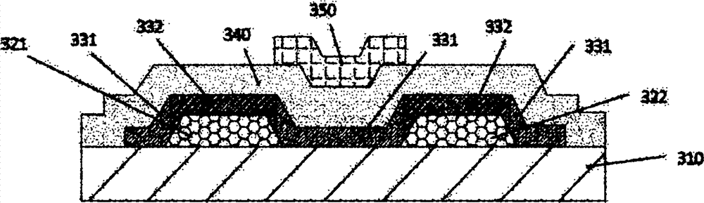
附图3为按照本发明提出的方法制造出的顶栅金属氧化物薄膜晶体管结构示意图,其基本结构如下:形成于玻璃衬底310上,包含一漏电极层321和源电极层322,一金属氧化物层330,一栅绝缘层340,一栅电极层350。Accompanying drawing 3 is the structure diagram of the top gate metal oxide thin film transistor manufactured according to the method proposed by the present invention, and its basic structure is as follows: formed on the
所述源漏电极层位于玻璃衬底上,通常由金属铝、钼、铬等材料构成,在大尺寸平板显示背板技术中源漏电极层一般由铝钕/钼铌合金构成,既能获得好的导电特性又能防止薄膜表面出现“小丘”等不良。源漏电极层的厚度通常为300纳米左右。The source-drain electrode layer is located on a glass substrate and is usually made of metal aluminum, molybdenum, chromium and other materials. In large-size flat panel display backplane technology, the source-drain electrode layer is generally made of aluminum neodymium/molybdenum-niobium alloy, which can obtain Good electrical conductivity can prevent defects such as "hills" on the surface of the film. The thickness of the source-drain electrode layer is usually about 300 nanometers.
所述金属氧化物层位于源漏电极层之上且在沟道区域附近与源漏电极交叠,可以为氧化锌(ZnO)为代表的多晶金属氧化物材料,也可以是铟镓锌氧(IGZO)为代表的非晶金属氧化物材料。其特征是:金属氧化物层根据导电特性的不同分成两个区域,即导体区域和半导体区域。位于源漏极正上方区域的金属氧化物薄膜呈现导体特性;其它区域金属氧化物呈现半导体特性。金属氧化物层的厚度可以在100-300纳米范围内。The metal oxide layer is located on the source-drain electrode layer and overlaps the source-drain electrode near the channel region, and may be a polycrystalline metal oxide material represented by zinc oxide (ZnO), or an indium gallium zinc oxide (IGZO) is the representative amorphous metal oxide material. It is characterized in that: the metal oxide layer is divided into two regions according to different conductivity characteristics, that is, a conductor region and a semiconductor region. The metal oxide thin film in the area directly above the source and drain exhibits conductor properties; the metal oxide in other areas exhibits semiconductor properties. The thickness of the metal oxide layer may be in the range of 100-300 nanometers.
所述栅绝缘层位于金属氧化物层和源漏电极层之上且覆盖上述两层薄膜,通常由二氧化硅或氮化硅构成,薄膜厚度为300纳米左右。The gate insulating layer is located on the metal oxide layer and the source-drain electrode layer and covers the above two thin films, usually made of silicon dioxide or silicon nitride, with a film thickness of about 300 nanometers.
所述栅电极层位于栅绝缘层上,通常由金属铝、钼、铬等材料构成。在大尺寸平板显示背板技术中栅电极层一般由钼铌/铝钕/钼铌合金构成,既能获得好的导电特性又能防止薄膜表面出现“小丘”等不良。栅电极层厚度通常为300纳米左右。The gate electrode layer is located on the gate insulating layer and is usually made of metal aluminum, molybdenum, chromium and other materials. In large-size flat panel display backplane technology, the gate electrode layer is generally composed of molybdenum-niobium/aluminum-neodymium/molybdenum-niobium alloy, which can not only obtain good electrical conductivity but also prevent defects such as "hills" on the surface of the film. The thickness of the gate electrode layer is usually about 300 nanometers.
与现有技术相比,本发明制备的金属氧化物薄膜晶体管的源漏电极与高载流子浓度的金属氧化物薄膜(即导体)直接接触,而不是常见技术中源漏电极与氧化物半导体接触的结构。这样因为隧道效应源漏电极与有源层之间会形成可靠的欧姆接触。本发明充分利用了金属氧化物材料在不同工艺条件下可分呈半导体和导体的特点,将源漏极上方的金属氧化物转化为导体,在源漏电极与金属氧化物间形成可靠的欧姆接触,从而增大了开态电流,解决了显示驱动中充电不足的技术难题。Compared with the prior art, the source and drain electrodes of the metal oxide thin film transistor prepared by the present invention are in direct contact with the metal oxide film (i.e. conductor) with high carrier concentration, instead of the source and drain electrodes in the common technology and the oxide semiconductor contact structure. In this way, a reliable ohmic contact will be formed between the source and drain electrodes and the active layer due to the tunnel effect. The invention makes full use of the characteristics that metal oxide materials can be divided into semiconductors and conductors under different process conditions, converts the metal oxide above the source and drain electrodes into conductors, and forms a reliable ohmic contact between the source and drain electrodes and the metal oxide , thereby increasing the on-state current and solving the technical problem of insufficient charging in display driving.
Claims (6)
Priority Applications (1)
| Application Number | Priority Date | Filing Date | Title |
|---|---|---|---|
| CN 201110009753 CN102157564B (en) | 2011-01-18 | 2011-01-18 | Preparation method of top gate metal oxide thin film transistor (TFT) |
Applications Claiming Priority (1)
| Application Number | Priority Date | Filing Date | Title |
|---|---|---|---|
| CN 201110009753 CN102157564B (en) | 2011-01-18 | 2011-01-18 | Preparation method of top gate metal oxide thin film transistor (TFT) |
Publications (2)
| Publication Number | Publication Date |
|---|---|
| CN102157564A CN102157564A (en) | 2011-08-17 |
| CN102157564B true CN102157564B (en) | 2013-05-01 |
Family
ID=44438896
Family Applications (1)
| Application Number | Title | Priority Date | Filing Date |
|---|---|---|---|
| CN 201110009753 Expired - Fee Related CN102157564B (en) | 2011-01-18 | 2011-01-18 | Preparation method of top gate metal oxide thin film transistor (TFT) |
Country Status (1)
| Country | Link |
|---|---|
| CN (1) | CN102157564B (en) |
Families Citing this family (14)
| Publication number | Priority date | Publication date | Assignee | Title |
|---|---|---|---|---|
| TWI458150B (en) * | 2012-01-11 | 2014-10-21 | E Ink Holdings Inc | Thin film transistor |
| CN102790012A (en) * | 2012-07-20 | 2012-11-21 | 京东方科技集团股份有限公司 | Array substrate and manufacturing method thereof as well as display equipment |
| CN103000530B (en) * | 2012-11-13 | 2015-05-20 | 深圳丹邦投资集团有限公司 | Manufacturing method of top-gate oxide thin-film transistor |
| CN103021959B (en) * | 2012-11-30 | 2014-09-17 | 京东方科技集团股份有限公司 | Array substrate, manufacture method of array substrate and display device |
| CN103050412B (en) * | 2012-12-20 | 2015-10-21 | 深圳丹邦投资集团有限公司 | The manufacture method of oxide thin film transistor |
| TWI687748B (en) * | 2013-06-05 | 2020-03-11 | 日商半導體能源研究所股份有限公司 | Display device and electronic device |
| CN103474439B (en) * | 2013-09-26 | 2016-08-24 | 合肥京东方光电科技有限公司 | A kind of display device, array base palte and preparation method thereof |
| CN105206570B (en) * | 2015-10-27 | 2018-11-23 | 深圳市华星光电技术有限公司 | A kind of display panel and its manufacturing method |
| CN106783624A (en) * | 2016-12-31 | 2017-05-31 | 杭州潮盛科技有限公司 | Transistor threshold voltage adjusting method and phase inverter preparation method |
| CN107464776B (en) * | 2017-08-30 | 2020-05-26 | 京东方科技集团股份有限公司 | Display panel, manufacturing method thereof and display device |
| CN108461391B (en) * | 2018-04-03 | 2020-11-03 | 深圳市华星光电半导体显示技术有限公司 | Preparation method of IGZO active layer and oxide thin film transistor |
| CN108766890B (en) * | 2018-04-13 | 2020-10-02 | 北京理工大学 | Method for preparing metal oxide thin film transistor at low temperature |
| CN113253581B (en) * | 2021-05-13 | 2024-05-31 | 中国振华集团永光电子有限公司(国营第八七三厂) | Method for removing photoresist after ion implantation |
| CN114823916A (en) * | 2022-04-22 | 2022-07-29 | 北海惠科光电技术有限公司 | Thin film transistor, display panel and manufacturing method of thin film transistor |
Citations (3)
| Publication number | Priority date | Publication date | Assignee | Title |
|---|---|---|---|---|
| CN101478005A (en) * | 2009-02-13 | 2009-07-08 | 北京大学深圳研究生院 | Metal oxide thin-film transistor and manufacturing process thereof |
| WO2010071034A1 (en) * | 2008-12-19 | 2010-06-24 | Semiconductor Energy Laboratory Co., Ltd. | Method for manufacturing transistor |
| CN101859799A (en) * | 2009-04-02 | 2010-10-13 | 株式会社半导体能源研究所 | Semiconductor device and method of manufacturing same |
-
2011
- 2011-01-18 CN CN 201110009753 patent/CN102157564B/en not_active Expired - Fee Related
Patent Citations (3)
| Publication number | Priority date | Publication date | Assignee | Title |
|---|---|---|---|---|
| WO2010071034A1 (en) * | 2008-12-19 | 2010-06-24 | Semiconductor Energy Laboratory Co., Ltd. | Method for manufacturing transistor |
| CN101478005A (en) * | 2009-02-13 | 2009-07-08 | 北京大学深圳研究生院 | Metal oxide thin-film transistor and manufacturing process thereof |
| CN101859799A (en) * | 2009-04-02 | 2010-10-13 | 株式会社半导体能源研究所 | Semiconductor device and method of manufacturing same |
Also Published As
| Publication number | Publication date |
|---|---|
| CN102157564A (en) | 2011-08-17 |
Similar Documents
| Publication | Publication Date | Title |
|---|---|---|
| CN102157564B (en) | Preparation method of top gate metal oxide thin film transistor (TFT) | |
| CN102157562B (en) | Method for manufacturing bottom gate metal oxide thin film transistor | |
| CN102157563B (en) | Metal Oxide Thin Film Transistor Fabrication Method | |
| JP6006558B2 (en) | Semiconductor device and manufacturing method thereof | |
| JP6134230B2 (en) | Thin film transistor and display device | |
| CN107799570A (en) | Top-gated autoregistration metal-oxide semiconductor (MOS) TFT and preparation method thereof | |
| Hu et al. | Effect of ITO serving as a barrier layer for Cu electrodes on performance of a-IGZO TFT | |
| WO2018010214A1 (en) | Method for manufacturing metal oxide thin film transistor array substrate | |
| TWI515793B (en) | Method for depositing thin film electrode and film stack | |
| CN108550625A (en) | A kind of thin film transistor and its manufacturing method | |
| CN107946364A (en) | Inorganic, metal oxide thin film transistor (TFT) and its manufacture method with compound crystal form | |
| JP5291105B2 (en) | Method for manufacturing field effect transistor | |
| CN108735821B (en) | Praseodymium-indium-zinc oxide thin film transistor and preparation method thereof | |
| CN107623040A (en) | A kind of indium gallium zinc oxide thin film transistor (TFT) and its manufacture method | |
| CN103400765B (en) | The manufacture method of oxide thin film transistor | |
| WO2015188476A1 (en) | Thin film transistor and manufacturing method therefor, oled back panel and display device | |
| CN107104151A (en) | A kind of double grid electrode metal oxide thin-film transistor and preparation method thereof | |
| CN106298880B (en) | Oxide thin film and preparation method, transistor and preparation method, display backplane | |
| CN107403832A (en) | A kind of high performance thin film transistor and application thereof | |
| CN108336135A (en) | A kind of neodymium indium-zinc oxide thin film transistor (TFT) and preparation method thereof | |
| CN106972063A (en) | The preparation method of metal oxide thin-film transistor | |
| CN105355663B (en) | A kind of hydrogen passive oxidation zinc-base double channel layer film transistor and preparation method thereof | |
| CN112002762B (en) | A gradient channel nitrogen-doped zinc oxide thin film transistor and its preparation method | |
| CN108288651A (en) | A kind of method that full magnetron sputtering prepares all-transparent top-grate structure thin film transistor | |
| CN106206745B (en) | A kind of manufacturing method of high mobility metal oxide TFT |
Legal Events
| Date | Code | Title | Description |
|---|---|---|---|
| C06 | Publication | ||
| PB01 | Publication | ||
| C10 | Entry into substantive examination | ||
| SE01 | Entry into force of request for substantive examination | ||
| C14 | Grant of patent or utility model | ||
| GR01 | Patent grant | ||
| CF01 | Termination of patent right due to non-payment of annual fee |
Granted publication date: 20130501 Termination date: 20200118 |
|
| CF01 | Termination of patent right due to non-payment of annual fee |